US5327008A - Semiconductor device having universal low-stress die support and method for making the same - Google Patents
Semiconductor device having universal low-stress die support and method for making the sameDownload PDFInfo
- Publication number
- US5327008A US5327008AUS08/035,422US3542293AUS5327008AUS 5327008 AUS5327008 AUS 5327008AUS 3542293 AUS3542293 AUS 3542293AUS 5327008 AUS5327008 AUS 5327008A
- Authority
- US
- United States
- Prior art keywords
- die
- tie bars
- semiconductor
- flag
- portions
- Prior art date
- Legal status (The legal status is an assumption and is not a legal conclusion. Google has not performed a legal analysis and makes no representation as to the accuracy of the status listed.)
- Expired - Lifetime
Links
Images


Classifications
- H—ELECTRICITY
- H01—ELECTRIC ELEMENTS
- H01L—SEMICONDUCTOR DEVICES NOT COVERED BY CLASS H10
- H01L23/00—Details of semiconductor or other solid state devices
- H01L23/48—Arrangements for conducting electric current to or from the solid state body in operation, e.g. leads, terminal arrangements ; Selection of materials therefor
- H—ELECTRICITY
- H01—ELECTRIC ELEMENTS
- H01L—SEMICONDUCTOR DEVICES NOT COVERED BY CLASS H10
- H01L24/00—Arrangements for connecting or disconnecting semiconductor or solid-state bodies; Methods or apparatus related thereto
- H01L24/01—Means for bonding being attached to, or being formed on, the surface to be connected, e.g. chip-to-package, die-attach, "first-level" interconnects; Manufacturing methods related thereto
- H01L24/26—Layer connectors, e.g. plate connectors, solder or adhesive layers; Manufacturing methods related thereto
- H01L24/31—Structure, shape, material or disposition of the layer connectors after the connecting process
- H01L24/32—Structure, shape, material or disposition of the layer connectors after the connecting process of an individual layer connector
- H—ELECTRICITY
- H01—ELECTRIC ELEMENTS
- H01L—SEMICONDUCTOR DEVICES NOT COVERED BY CLASS H10
- H01L23/00—Details of semiconductor or other solid state devices
- H01L23/48—Arrangements for conducting electric current to or from the solid state body in operation, e.g. leads, terminal arrangements ; Selection of materials therefor
- H01L23/488—Arrangements for conducting electric current to or from the solid state body in operation, e.g. leads, terminal arrangements ; Selection of materials therefor consisting of soldered or bonded constructions
- H01L23/495—Lead-frames or other flat leads
- H01L23/49503—Lead-frames or other flat leads characterised by the die pad
- H—ELECTRICITY
- H01—ELECTRIC ELEMENTS
- H01L—SEMICONDUCTOR DEVICES NOT COVERED BY CLASS H10
- H01L2224/00—Indexing scheme for arrangements for connecting or disconnecting semiconductor or solid-state bodies and methods related thereto as covered by H01L24/00
- H01L2224/01—Means for bonding being attached to, or being formed on, the surface to be connected, e.g. chip-to-package, die-attach, "first-level" interconnects; Manufacturing methods related thereto
- H01L2224/02—Bonding areas; Manufacturing methods related thereto
- H01L2224/04—Structure, shape, material or disposition of the bonding areas prior to the connecting process
- H01L2224/05—Structure, shape, material or disposition of the bonding areas prior to the connecting process of an individual bonding area
- H01L2224/0554—External layer
- H01L2224/0555—Shape
- H01L2224/05552—Shape in top view
- H01L2224/05553—Shape in top view being rectangular
- H—ELECTRICITY
- H01—ELECTRIC ELEMENTS
- H01L—SEMICONDUCTOR DEVICES NOT COVERED BY CLASS H10
- H01L2224/00—Indexing scheme for arrangements for connecting or disconnecting semiconductor or solid-state bodies and methods related thereto as covered by H01L24/00
- H01L2224/01—Means for bonding being attached to, or being formed on, the surface to be connected, e.g. chip-to-package, die-attach, "first-level" interconnects; Manufacturing methods related thereto
- H01L2224/02—Bonding areas; Manufacturing methods related thereto
- H01L2224/04—Structure, shape, material or disposition of the bonding areas prior to the connecting process
- H01L2224/05—Structure, shape, material or disposition of the bonding areas prior to the connecting process of an individual bonding area
- H01L2224/0554—External layer
- H01L2224/0555—Shape
- H01L2224/05552—Shape in top view
- H01L2224/05554—Shape in top view being square
- H—ELECTRICITY
- H01—ELECTRIC ELEMENTS
- H01L—SEMICONDUCTOR DEVICES NOT COVERED BY CLASS H10
- H01L2224/00—Indexing scheme for arrangements for connecting or disconnecting semiconductor or solid-state bodies and methods related thereto as covered by H01L24/00
- H01L2224/01—Means for bonding being attached to, or being formed on, the surface to be connected, e.g. chip-to-package, die-attach, "first-level" interconnects; Manufacturing methods related thereto
- H01L2224/26—Layer connectors, e.g. plate connectors, solder or adhesive layers; Manufacturing methods related thereto
- H01L2224/28—Structure, shape, material or disposition of the layer connectors prior to the connecting process
- H01L2224/29—Structure, shape, material or disposition of the layer connectors prior to the connecting process of an individual layer connector
- H01L2224/29001—Core members of the layer connector
- H01L2224/29005—Structure
- H01L2224/29007—Layer connector smaller than the underlying bonding area
- H—ELECTRICITY
- H01—ELECTRIC ELEMENTS
- H01L—SEMICONDUCTOR DEVICES NOT COVERED BY CLASS H10
- H01L2224/00—Indexing scheme for arrangements for connecting or disconnecting semiconductor or solid-state bodies and methods related thereto as covered by H01L24/00
- H01L2224/01—Means for bonding being attached to, or being formed on, the surface to be connected, e.g. chip-to-package, die-attach, "first-level" interconnects; Manufacturing methods related thereto
- H01L2224/26—Layer connectors, e.g. plate connectors, solder or adhesive layers; Manufacturing methods related thereto
- H01L2224/31—Structure, shape, material or disposition of the layer connectors after the connecting process
- H01L2224/32—Structure, shape, material or disposition of the layer connectors after the connecting process of an individual layer connector
- H01L2224/3201—Structure
- H01L2224/32012—Structure relative to the bonding area, e.g. bond pad
- H01L2224/32014—Structure relative to the bonding area, e.g. bond pad the layer connector being smaller than the bonding area, e.g. bond pad
- H—ELECTRICITY
- H01—ELECTRIC ELEMENTS
- H01L—SEMICONDUCTOR DEVICES NOT COVERED BY CLASS H10
- H01L2224/00—Indexing scheme for arrangements for connecting or disconnecting semiconductor or solid-state bodies and methods related thereto as covered by H01L24/00
- H01L2224/01—Means for bonding being attached to, or being formed on, the surface to be connected, e.g. chip-to-package, die-attach, "first-level" interconnects; Manufacturing methods related thereto
- H01L2224/26—Layer connectors, e.g. plate connectors, solder or adhesive layers; Manufacturing methods related thereto
- H01L2224/31—Structure, shape, material or disposition of the layer connectors after the connecting process
- H01L2224/32—Structure, shape, material or disposition of the layer connectors after the connecting process of an individual layer connector
- H01L2224/321—Disposition
- H01L2224/32151—Disposition the layer connector connecting between a semiconductor or solid-state body and an item not being a semiconductor or solid-state body, e.g. chip-to-substrate, chip-to-passive
- H01L2224/32221—Disposition the layer connector connecting between a semiconductor or solid-state body and an item not being a semiconductor or solid-state body, e.g. chip-to-substrate, chip-to-passive the body and the item being stacked
- H01L2224/32245—Disposition the layer connector connecting between a semiconductor or solid-state body and an item not being a semiconductor or solid-state body, e.g. chip-to-substrate, chip-to-passive the body and the item being stacked the item being metallic
- H—ELECTRICITY
- H01—ELECTRIC ELEMENTS
- H01L—SEMICONDUCTOR DEVICES NOT COVERED BY CLASS H10
- H01L2224/00—Indexing scheme for arrangements for connecting or disconnecting semiconductor or solid-state bodies and methods related thereto as covered by H01L24/00
- H01L2224/01—Means for bonding being attached to, or being formed on, the surface to be connected, e.g. chip-to-package, die-attach, "first-level" interconnects; Manufacturing methods related thereto
- H01L2224/42—Wire connectors; Manufacturing methods related thereto
- H01L2224/47—Structure, shape, material or disposition of the wire connectors after the connecting process
- H01L2224/48—Structure, shape, material or disposition of the wire connectors after the connecting process of an individual wire connector
- H01L2224/4805—Shape
- H01L2224/4809—Loop shape
- H01L2224/48091—Arched
- H—ELECTRICITY
- H01—ELECTRIC ELEMENTS
- H01L—SEMICONDUCTOR DEVICES NOT COVERED BY CLASS H10
- H01L2224/00—Indexing scheme for arrangements for connecting or disconnecting semiconductor or solid-state bodies and methods related thereto as covered by H01L24/00
- H01L2224/01—Means for bonding being attached to, or being formed on, the surface to be connected, e.g. chip-to-package, die-attach, "first-level" interconnects; Manufacturing methods related thereto
- H01L2224/42—Wire connectors; Manufacturing methods related thereto
- H01L2224/47—Structure, shape, material or disposition of the wire connectors after the connecting process
- H01L2224/48—Structure, shape, material or disposition of the wire connectors after the connecting process of an individual wire connector
- H01L2224/481—Disposition
- H01L2224/48151—Connecting between a semiconductor or solid-state body and an item not being a semiconductor or solid-state body, e.g. chip-to-substrate, chip-to-passive
- H01L2224/48221—Connecting between a semiconductor or solid-state body and an item not being a semiconductor or solid-state body, e.g. chip-to-substrate, chip-to-passive the body and the item being stacked
- H01L2224/48245—Connecting between a semiconductor or solid-state body and an item not being a semiconductor or solid-state body, e.g. chip-to-substrate, chip-to-passive the body and the item being stacked the item being metallic
- H01L2224/48247—Connecting between a semiconductor or solid-state body and an item not being a semiconductor or solid-state body, e.g. chip-to-substrate, chip-to-passive the body and the item being stacked the item being metallic connecting the wire to a bond pad of the item
- H—ELECTRICITY
- H01—ELECTRIC ELEMENTS
- H01L—SEMICONDUCTOR DEVICES NOT COVERED BY CLASS H10
- H01L2224/00—Indexing scheme for arrangements for connecting or disconnecting semiconductor or solid-state bodies and methods related thereto as covered by H01L24/00
- H01L2224/01—Means for bonding being attached to, or being formed on, the surface to be connected, e.g. chip-to-package, die-attach, "first-level" interconnects; Manufacturing methods related thereto
- H01L2224/42—Wire connectors; Manufacturing methods related thereto
- H01L2224/47—Structure, shape, material or disposition of the wire connectors after the connecting process
- H01L2224/48—Structure, shape, material or disposition of the wire connectors after the connecting process of an individual wire connector
- H01L2224/484—Connecting portions
- H01L2224/48463—Connecting portions the connecting portion on the bonding area of the semiconductor or solid-state body being a ball bond
- H01L2224/48465—Connecting portions the connecting portion on the bonding area of the semiconductor or solid-state body being a ball bond the other connecting portion not on the bonding area being a wedge bond, i.e. ball-to-wedge, regular stitch
- H—ELECTRICITY
- H01—ELECTRIC ELEMENTS
- H01L—SEMICONDUCTOR DEVICES NOT COVERED BY CLASS H10
- H01L2224/00—Indexing scheme for arrangements for connecting or disconnecting semiconductor or solid-state bodies and methods related thereto as covered by H01L24/00
- H01L2224/73—Means for bonding being of different types provided for in two or more of groups H01L2224/10, H01L2224/18, H01L2224/26, H01L2224/34, H01L2224/42, H01L2224/50, H01L2224/63, H01L2224/71
- H01L2224/732—Location after the connecting process
- H01L2224/73251—Location after the connecting process on different surfaces
- H01L2224/73265—Layer and wire connectors
- H—ELECTRICITY
- H01—ELECTRIC ELEMENTS
- H01L—SEMICONDUCTOR DEVICES NOT COVERED BY CLASS H10
- H01L24/00—Arrangements for connecting or disconnecting semiconductor or solid-state bodies; Methods or apparatus related thereto
- H01L24/01—Means for bonding being attached to, or being formed on, the surface to be connected, e.g. chip-to-package, die-attach, "first-level" interconnects; Manufacturing methods related thereto
- H01L24/42—Wire connectors; Manufacturing methods related thereto
- H01L24/47—Structure, shape, material or disposition of the wire connectors after the connecting process
- H01L24/48—Structure, shape, material or disposition of the wire connectors after the connecting process of an individual wire connector
- H—ELECTRICITY
- H01—ELECTRIC ELEMENTS
- H01L—SEMICONDUCTOR DEVICES NOT COVERED BY CLASS H10
- H01L24/00—Arrangements for connecting or disconnecting semiconductor or solid-state bodies; Methods or apparatus related thereto
- H01L24/73—Means for bonding being of different types provided for in two or more of groups H01L24/10, H01L24/18, H01L24/26, H01L24/34, H01L24/42, H01L24/50, H01L24/63, H01L24/71
- H—ELECTRICITY
- H01—ELECTRIC ELEMENTS
- H01L—SEMICONDUCTOR DEVICES NOT COVERED BY CLASS H10
- H01L2924/00—Indexing scheme for arrangements or methods for connecting or disconnecting semiconductor or solid-state bodies as covered by H01L24/00
- H01L2924/0001—Technical content checked by a classifier
- H01L2924/00014—Technical content checked by a classifier the subject-matter covered by the group, the symbol of which is combined with the symbol of this group, being disclosed without further technical details
- H—ELECTRICITY
- H01—ELECTRIC ELEMENTS
- H01L—SEMICONDUCTOR DEVICES NOT COVERED BY CLASS H10
- H01L2924/00—Indexing scheme for arrangements or methods for connecting or disconnecting semiconductor or solid-state bodies as covered by H01L24/00
- H01L2924/01—Chemical elements
- H01L2924/01013—Aluminum [Al]
- H—ELECTRICITY
- H01—ELECTRIC ELEMENTS
- H01L—SEMICONDUCTOR DEVICES NOT COVERED BY CLASS H10
- H01L2924/00—Indexing scheme for arrangements or methods for connecting or disconnecting semiconductor or solid-state bodies as covered by H01L24/00
- H01L2924/01—Chemical elements
- H01L2924/01014—Silicon [Si]
- H—ELECTRICITY
- H01—ELECTRIC ELEMENTS
- H01L—SEMICONDUCTOR DEVICES NOT COVERED BY CLASS H10
- H01L2924/00—Indexing scheme for arrangements or methods for connecting or disconnecting semiconductor or solid-state bodies as covered by H01L24/00
- H01L2924/01—Chemical elements
- H01L2924/01029—Copper [Cu]
- H—ELECTRICITY
- H01—ELECTRIC ELEMENTS
- H01L—SEMICONDUCTOR DEVICES NOT COVERED BY CLASS H10
- H01L2924/00—Indexing scheme for arrangements or methods for connecting or disconnecting semiconductor or solid-state bodies as covered by H01L24/00
- H01L2924/01—Chemical elements
- H01L2924/01033—Arsenic [As]
- H—ELECTRICITY
- H01—ELECTRIC ELEMENTS
- H01L—SEMICONDUCTOR DEVICES NOT COVERED BY CLASS H10
- H01L2924/00—Indexing scheme for arrangements or methods for connecting or disconnecting semiconductor or solid-state bodies as covered by H01L24/00
- H01L2924/01—Chemical elements
- H01L2924/01047—Silver [Ag]
- H—ELECTRICITY
- H01—ELECTRIC ELEMENTS
- H01L—SEMICONDUCTOR DEVICES NOT COVERED BY CLASS H10
- H01L2924/00—Indexing scheme for arrangements or methods for connecting or disconnecting semiconductor or solid-state bodies as covered by H01L24/00
- H01L2924/01—Chemical elements
- H01L2924/01082—Lead [Pb]
- H—ELECTRICITY
- H01—ELECTRIC ELEMENTS
- H01L—SEMICONDUCTOR DEVICES NOT COVERED BY CLASS H10
- H01L2924/00—Indexing scheme for arrangements or methods for connecting or disconnecting semiconductor or solid-state bodies as covered by H01L24/00
- H01L2924/10—Details of semiconductor or other solid state devices to be connected
- H01L2924/1015—Shape
- H01L2924/1016—Shape being a cuboid
- H01L2924/10162—Shape being a cuboid with a square active surface
- H—ELECTRICITY
- H01—ELECTRIC ELEMENTS
- H01L—SEMICONDUCTOR DEVICES NOT COVERED BY CLASS H10
- H01L2924/00—Indexing scheme for arrangements or methods for connecting or disconnecting semiconductor or solid-state bodies as covered by H01L24/00
- H01L2924/10—Details of semiconductor or other solid state devices to be connected
- H01L2924/11—Device type
- H01L2924/14—Integrated circuits
- H—ELECTRICITY
- H01—ELECTRIC ELEMENTS
- H01L—SEMICONDUCTOR DEVICES NOT COVERED BY CLASS H10
- H01L2924/00—Indexing scheme for arrangements or methods for connecting or disconnecting semiconductor or solid-state bodies as covered by H01L24/00
- H01L2924/15—Details of package parts other than the semiconductor or other solid state devices to be connected
- H01L2924/181—Encapsulation
- Y—GENERAL TAGGING OF NEW TECHNOLOGICAL DEVELOPMENTS; GENERAL TAGGING OF CROSS-SECTIONAL TECHNOLOGIES SPANNING OVER SEVERAL SECTIONS OF THE IPC; TECHNICAL SUBJECTS COVERED BY FORMER USPC CROSS-REFERENCE ART COLLECTIONS [XRACs] AND DIGESTS
- Y10—TECHNICAL SUBJECTS COVERED BY FORMER USPC
- Y10T—TECHNICAL SUBJECTS COVERED BY FORMER US CLASSIFICATION
- Y10T29/00—Metal working
- Y10T29/49—Method of mechanical manufacture
- Y10T29/49002—Electrical device making
- Y10T29/49117—Conductor or circuit manufacturing
- Y10T29/49121—Beam lead frame or beam lead device
Definitions
- the present inventionrelates generally to semiconductor devices, and more specifically to semiconductor devices which utilize universal die supports which lower stress in semiconductor packages, and methods for making the same.
- Package crackingis a common problem in plastic encapsulated semiconductor devices.
- the problemarises from a combination of factors.
- One factoris an internal delamination between the plastic encapsulant material and a flag of a lead frame.
- the flagis a plate-like member of a conventional lead frame which supports the die.
- the flaglike the rest of the lead frame, is usually made of copper, a copper-alloy, or an iron-nickel alloy, and therefore has a coefficient of thermal expansion (CTE) which in most instances is different than that of the surrounding molding compound or plastic.
- CTEcoefficient of thermal expansion
- a window-frame flagis more or less a hollowed-frame that supports the die, rather than a solid paddle.
- the methods described abovedo, to some extent, decrease the possibility of delamination by providing better adhesion to the plastic encapsulating material.
- the present inventionhas the advantage of reduced delamination, albeit through a technique not previously used.
- the present inventionaddresses another manufacturing problem which the above methods do not address, namely the need for semiconductor manufacturers to use a different or customized lead frame design for each of its products. Having a different lead frame design for each die size and die functional pin-out necessitates a large inventory of piece-parts and requires additional time and human resources to design a new lead frame before each product introduction. In addition to costs associated with inventory and design, the cost of the lead frames themselves are undesirably inflated because of insufficient volume to lower the cost to a minimum.
- the present inventionachieves this goal by utilizing a lead frame in a semiconductor device which can be used with various die sizes, while at the same time improving adhesion between the lead frame and the encapsulating material to alleviate package cracking problems.
- a semiconductor devicehas a plurality leads which define a die receiving area and a tie bar which traverses the die receiving.
- a semiconductor dieis mount on, and supported by, the tie bar in the die receiving area.
- the dieis electrically coupled to the plurality of leads and is encapsulated in a package body.
- a mini-flagis integrated into the tie bar such that the mini-flag and tie bar together support the die. Also within the scope of the invention are methods for making these semiconductor devices.
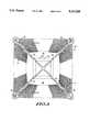
- FIG. 1is a top-down plan view of portions of an unpackaged, flagless semiconductor device in accordance with the present invention.
- FIG. 2is a cross-sectional view of the semiconductor device of FIG. 1 taken along the line 2--2, as packaged in plastic.
- FIG. 3is a top-down plan view of portions of an alternative lead frame design suitable for use in the present invention.
- FIG. 4is a top-down plan view of portions of yet another lead frame design for use in one embodiment of the present invention which utilizes a mini-flag.
- FIG. 5is a cross-sectional view a packaged semiconductor device in accordance with the present invention which utilizes the lead frame of FIG. 4.
- FIG. 6is a top-down view of portions of an alternative lead frame design having a mini-flag, also suited for use in accordance with the present invention.
- FIG. 7is a top-down view of portions of yet another lead frame design having a mini-flag suited for use with the present invention.
- FIG. 1illustrates these advantages in a top-down plan view of one embodiment of the present invention.
- a semiconductor device 10has portions of a lead frame 12 which include a plurality of leads 14 and four tie bars 16. Lead frame 12 of FIG. 1 is only partially illustrated. As one of ordinary skill in the art would understand, leads 14 and tie bars 16 extend to two opposing rails (not illustrated) as in a conventional strip lead frame. In addition, not all of the leads of lead frame 12 are illustrated.
- the plurality of leads 14each have inner lead portions which together define a die receiving area 18 within the device.
- the particular lead frame illustrated in FIG. 1is for use in a QFP (quad flat pack) semiconductor package; however, it is important to realize the present invention is not limited to such a package type, as will become evident later in the description.
- QFPquad flat pack
- each tie bar 16originates at a corner of device 10 and extends into die receiving area 18 until converging with the other tie bars to form an "X".
- tie bars 16could extend from opposing sides of the die receiving area to form a "+" as viewed from the perspective of FIG. 1.
- Die 20is typically an integrated circuit, such as a microprocessor, a memory, an analog device, or the like, which is fabricated on silicon or another semiconducting substrate.
- Die 20includes a plurality of conductive bond pads 22 used to electrically access portions of the integrated circuit through various conducting layers (not shown) of the die.
- the electrical accessibility to the circuitis extended externally through a combination of conventional wire bonds 24 and leads 14.
- Wire bonds 24electrically couple bonds pads 22 to respectively leads 14. As depicted in FIG. 2, leads 14 extend outside of a package body 28 to provide external accessibility to the end device user.
- tie bars 16each have two distinct portions with different widths.
- a first portion 15 having a first widthextends from the rails (not shown) into die receiving area 18.
- a second portion 17actually supports die 20.
- Portions 17each have a second width which is larger than the first width.
- the reason for the two different widthsis not that die 20 cannot be supported by a narrower tie bar. As will become evident in FIG. 3, it is the configuration of the tie bars, not the width, that establishes adequate die support strength and stability. Instead, the reason two tie bar portions having different widths is used is to establish "shoulders" 19. Shoulders 19 provide a reference point used to align die 20 on the tie bars.
- Vision-based die bonding equipmentcan easily locate shoulders 19, thereby enabling accurate placement of die 20 onto the tie bars. As illustrated, each shoulder 19 is approximately parallel with a side of die 20. Features other than shoulders 19 can be used to aid in die mounting, as will also become evident in FIG. 3. It is important to note, however, that use of such die alignment features is not an essential aspect of the present invention.
- FIG. 1demonstrates the universal aspect of device 10. Due to the configuration of tie bars 16 of lead frame 12, several different semiconductor die sizes and shapes can be used. Conventional devices typically employ lead frames having a flag, onto which a semiconductor die is mounted. The flag is made slightly larger than the die to provide a large die bonding area, thereby maximizing the adhesion between the die and the flag. In using such a flag, a semiconductor manufacture restricts which die can be used in the device. Thus for different die shapes and sizes, the manufacture must design a new lead frame. As discussed previously, new designs delay product introductions and add to manufacturing costs.
- a device in accordance with the present inventioneliminates many new lead frame designs in comparison to traditional methods. As illustrated in FIG. 1, device 10 does not employ a flag. Instead, die 20 rests on tie bars 16. Due to the configuration of tie bars 16, nearly any size or shape of die can be supported. A limitation to the die size and shape of die 20 is imposed by inner portions of leads 14 which define die receiving area 18. Another limitation to the die size used with lead frame 12 may be wire bond length. As the die size becomes smaller, the length of wire bonds 24 needed to electrically couple the die to leads 14 increases. Thus, a manufacturer's upper limit on wire bond length will also set a lower limit on die size.
- die sizecan be imposed by features in the tie bars. For instance, if shoulders 19 or other alignment features are used, mounting a die on the tie bars which covers the alignment features may defeat their initial purpose. However, use of shoulders or other alignment features does not prohibit variable dies sizes from being used. Although the distance from an alignment feature to the die may vary with different die sizes, several different die sizes can still be used with the same lead frame design. For example, die sizes smaller than die 20 can still be mounted onto tie bars 16.
- Another tie bar feature which limits die sizemay be down-set regions, such as down-set regions 26 illustrated in FIG. 1. Portions 15 of the tie bars are approximately planar with leads 14, whereas portions 17 are in a lower plane as a result of down-set regions 26. The down-set feature is also illustrated in FIG.
- FIG. 2a cross-sectional view of device 10, as packaged, taken along the line 2--2 of FIG. 1.
- Down-set tie barsare used to lower the position of the die in comparison to leads to facilitate wire bonding. If tie bars 16 are designed to include down-set regions, the size of die 20 is further limited to an area within the down-set region to avoid mounting the die on noncoplanar tie bars.
- FIG. 2The cross-section of FIG, 2 aids in understanding how device 10 is also more resistant to package delamination when compared to devices which use conventional lead frames and flags
- Device 10 as illustrated in FIG. 2is packaged in a plastic resin package body 28,
- Package body 28is formed about the device using traditional plastic encapsulation methods, But unlike traditional plastic packages, package body 28 is less prone to cracking because die 20 is supported by tie bars 16. (In FIG. 2 it appears that only one tie bar supports the die because the cross-section is taken where all the tie bars converge to one point.)
- the reason why package body 28 is less prone to crackingis because the total interface area between the plastic package material and the die support (in this case, tie bars 16) is much less than the interface area in conventional devices.
- the interface between the die support member and the plasticis referred to as the plastic-metal interface rather than the plastic-flag interface since not all embodiments of the present invention have a flag.
- the plastic-metal interface within the die receiving areais equal to the area of the flag, which is slightly more than the area of the die.
- the plastic-metal interface areais considerably less, being equal to the surface area of the tie bars.
- the improvement in package cracking performance in device 10 and other embodiments of the present inventionis attributable to improved adhesion properties.
- delaminationtraditionally occurs between a flag and the plastic packaging material because of high stress and poor adhesion between the lead frame metals and conventional plastic encapsulation materials.
- the present inventionimproves the delamination problem by minimizing the plastic-metal interface area, thereby minimizing the potential delamination area. Decreasing the interface area between the lead frame and plastic results in an increase in the interface area between the plastic packaging and the backside of the semiconductor die, herein referred to as the plastic-die interface.
- the increase in the plastic-die interface areais advantageous because adhesion between plastic encapsulation materials and silicon (the most common semiconductor die material) is stronger than the adhesion between plastic and most lead frame metals. Accordingly, delamination is less likely to occur at the plastic-die interface than at the plastic-metal interface.
- FIG. 3illustrates portions of a lead frame 30 in a top-down plan view.
- Lead frame 30has various features which can be used in a semiconductor device in accordance with the present invention.
- lead frame 30has many features in common with lead frame 12 of FIG. 1. Accordingly, like numerals in each of the figures represent the same or similar elements.
- Four tie bars 32 of lead frame 30extend across die receiving area 18 to form an X-shaped die support (a semiconductor die is not illustrated in FIG. 3).
- each tie bar 32has a substantially constant width throughout die receiving area 18.
- An advantage in using tie bars 32 over tie bars 16is that with tie bars 32 there is a smaller plastic-metal interface area, thereby lowering the chances of delamination and package cracking.
- tie bars 32do not have shoulders to aid in die alignment. However, other features can be incorporated into tie bars 32 to assist in die mounting. A few of the possible types of features suited for this are illustrated in FIG. 3 as alignment features 34, 35, 36, and 37. An alignment feature is included in each of tie bars 32 to represent various types of alignment features which might be implemented. However, it is important to note that any number of tie bars can incorporate any number or type of alignment feature.
- FIG. 3also illustrates the universal nature of lead frame 30, showing that two different die sizes (represented in phantom as lines 38 and 39) can be used in conjunction with the same lead frame.
- FIG. 4illustrates, in a top-down plan view, portions of a lead frame 40 having such a mini-flag 42.
- Mini-flag 42is kept smaller in area than a semiconductor die (illustrated in phantom as line 44) to keep the total interface area between the mini-flag and a plastic encapsulation material (not illustrated) smaller than in conventional devices.
- the actual size of the mini-flagcan be optimized to meet processing and reliability requirements of a particular manufacturer. As a general rule, however, the area of mini-flag 42 should be less than 50 percent of the area of a semiconductor die mounted thereto.
- FIG. 5is a cross-sectional view of lead frame 40 incorporated into a semiconductor device 45 in accordance with the present invention.
- Other elements of device 45are similar to or are the same as other elements discussed in reference to previous embodiments and are thus labeled with the same reference numerals.
- a semiconductor device using a mini-flag in accordance with the present inventionremoves previous constraints on flag size, and also on flag shape. For instance, as illustrated in FIG. 6, portions of a lead frame 50 (only partially illustrated) can include a round mini-flag 52 to support a larger die (illustrated in phantom as line 54).
- a lead frame 60(only partially illustrated) has a plurality of leads 62, the inner portions of which define a die receiving area 63. Extending across die receiving area 63 are two tie bars 64. Lead frames which include two tie bars extending from opposing sides of the die receiving area are most commonly used in PDIP (plastic dual-in-line) devices. Like in previous lead frame illustrations, not all portions of the lead frame 60 are illustrated. For instance, one of ordinary skill in the art would realize that the tie bars and leads extend to rails of a lead frame strip, but neither the entire stripe nor the rails are illustrated.
- mini-flag 66is made to have an area smaller than the area of a semiconductor die mounted thereto (illustrated in phantom as line 68).
- Use of a mini-flagallows several different die sizes to be mounted onto mini-flag 66 without having to redesign the entire lead frame, thereby saving manufacturing costs.
- the reduced area of mini-flag 66results in a smaller plastic-metal interface, in comparison to conventional devices, once the lead frame is encapsulated by plastic. Thus, delamination and package cracking problems are less likely.
- die attach adhesivee.g. adhesive 21 in FIGS. 2 and 5
- die attach adhesivee.g. adhesive 21 in FIGS. 2 and 5
- an adhesive materialis usually applied in a predetermined pattern through a dispense head onto the flag.
- the die attach adhesive patternis now limited to, for example in device 10 of FIG. 1, the tie bar portions 17 beneath the die. Therefore, tooling modifications for adhesive dispense heads may be necessary. Also, the amount of die attach adhesive dispensed is reduced since the die support area is smaller. Tighter process control may also be needed for a couple of reasons.
- a fillet of die attach adhesiveis formed around the periphery of the semiconductor die.
- the filletsurrounds the periphery of the die support member.
- a suitable fillet for a die attach adhesive used in accordance with the present inventionis illustrated in FIGS. 2 and 5.
- Another processing modificationmay be useful during wire bonding. Since a semiconductor die is not fully supported along the die periphery, it may be advantageous to provide peripheral die support during wire bonding. Bond pads are generally, but not always, located around the periphery of the die. Thus, to bond a wire to each bond pad, a wire bonding tool must exert pressure on the die perimeter each time it forms a bond. If the wire bonding force is high enough, or alternatively if the die is not flexible enough, there is a risk that the force exerted will cause an unsupported portion of the die to crack or chip. Therefore, it may be desirable to incorporate a support mechanism into the wire bonding platform.
- the platformmay be designed to include a cut-out which matches the pattern and thickness of the tie bars (and if included the mini-flag) so together the platform and tie bars (and if included the mini-flag) form a substantially planar and continuous surface.
- the entire diewould be supported by a combination of the tie bars and platform during the wire bonding operation.
- a further advantage of having the die supported by a planar and continuous surfaceis to achieve even heating of the die during the wire bonding operation. It is important to note that modifications to existing wire bonding operations may not be needed in practicing the present invention. The need for modifications will depend on various factors, including bonding force, die thickness, die size, and bond pad location to name a few.
- tie bars which are used to support a semiconductor dieneed not be in an "X" configuration. Any configuration which will adequately support a die is contemplated as being suitable.
- the inventionis not limited to any particular number of tie bars to support a die. There is confusion in terminology as to the number of tie bars a particular device has.
- lead frame 60has one tie bar.
- the number of tie bars recited with respect to the present descriptionrefers to the number of places the tie bars are connected to rails of the lead frame. This is analogous to the number of places in which a tie bar is excised from a lead frame, to become flush with an edge or side of a package body.
- there are two tie bars in lead frame 60regardless of the presence of mini-flag 66, because the tie bars connect with rails (not illustrated) in two places.
- the number of tie bars usedis not as important as the nature of the tie bar configuration.
- the tie bar(s)form a die support member which is continuous across the entire die receiving area.
- the mini-flagcan be modified using any of several known methods to also improve package cracking performance.
- the mini-flagcan include dimples or small holes to improve adhesion.
- a mini-flagcan be a window-frame mini-flag.
- the present inventionis also adaptable to semiconductor devices employing a die-down configuration. In other words, a die may be mounted to tie bars (or a mini-flag) such that the active surface of the die is adjacent the die support. Such adaptations are within the scope of the present invention.
- the present inventionis not limited by any type of external lead configuration (e.g.
Landscapes
- Engineering & Computer Science (AREA)
- Computer Hardware Design (AREA)
- Microelectronics & Electronic Packaging (AREA)
- Power Engineering (AREA)
- Physics & Mathematics (AREA)
- Condensed Matter Physics & Semiconductors (AREA)
- General Physics & Mathematics (AREA)
- Lead Frames For Integrated Circuits (AREA)
Abstract
Description
Claims (24)
Priority Applications (11)
| Application Number | Priority Date | Filing Date | Title |
|---|---|---|---|
| US08/035,422US5327008A (en) | 1993-03-22 | 1993-03-22 | Semiconductor device having universal low-stress die support and method for making the same |
| US08/133,947US5424576A (en) | 1993-03-22 | 1993-10-12 | Semiconductor device having x-shaped die support member and method for making the same |
| SG1996003719ASG75769A1 (en) | 1993-03-22 | 1994-03-03 | Semiconductor device having x-shaped die support member and method for making the same |
| DE69430648TDE69430648T2 (en) | 1993-03-22 | 1994-03-03 | Semiconductor arrangement consisting of an X-shaped mounting frame and its manufacturing process |
| EP94103166AEP0617464B1 (en) | 1993-03-22 | 1994-03-03 | Semiconductor device having X-shaped die support member and method for making the same |
| SG200000981ASG97850A1 (en) | 1993-03-22 | 1994-03-03 | Semiconductor device having x-shaped die support member and method for making the same |
| JP6071548AJP2838160B2 (en) | 1993-03-22 | 1994-03-15 | Semiconductor device having X-shaped die support member |
| MYPI94000653AMY125704A (en) | 1993-03-22 | 1994-03-21 | Semiconductor device having x-shaped die support member and method for making the same. |
| CNA021548471ACN1514490A (en) | 1993-03-22 | 1994-03-21 | Semiconductor device having X shaped pipe core support and its manufacturing method |
| CN94103949ACN1118873C (en) | 1993-03-22 | 1994-03-21 | Semiconductor device with X-shaped die support |
| KR1019940005590AKR100219772B1 (en) | 1993-03-22 | 1994-03-21 | Semiconductor devices |
Applications Claiming Priority (1)
| Application Number | Priority Date | Filing Date | Title |
|---|---|---|---|
| US08/035,422US5327008A (en) | 1993-03-22 | 1993-03-22 | Semiconductor device having universal low-stress die support and method for making the same |
Related Child Applications (1)
| Application Number | Title | Priority Date | Filing Date |
|---|---|---|---|
| US08/133,947Continuation-In-PartUS5424576A (en) | 1993-03-22 | 1993-10-12 | Semiconductor device having x-shaped die support member and method for making the same |
Publications (1)
| Publication Number | Publication Date |
|---|---|
| US5327008Atrue US5327008A (en) | 1994-07-05 |
Family
ID=21882588
Family Applications (2)
| Application Number | Title | Priority Date | Filing Date |
|---|---|---|---|
| US08/035,422Expired - LifetimeUS5327008A (en) | 1993-03-22 | 1993-03-22 | Semiconductor device having universal low-stress die support and method for making the same |
| US08/133,947Expired - LifetimeUS5424576A (en) | 1993-03-22 | 1993-10-12 | Semiconductor device having x-shaped die support member and method for making the same |
Family Applications After (1)
| Application Number | Title | Priority Date | Filing Date |
|---|---|---|---|
| US08/133,947Expired - LifetimeUS5424576A (en) | 1993-03-22 | 1993-10-12 | Semiconductor device having x-shaped die support member and method for making the same |
Country Status (4)
| Country | Link |
|---|---|
| US (2) | US5327008A (en) |
| KR (1) | KR100219772B1 (en) |
| MY (1) | MY125704A (en) |
| SG (1) | SG97850A1 (en) |
Cited By (162)
| Publication number | Priority date | Publication date | Assignee | Title |
|---|---|---|---|---|
| US5424576A (en)* | 1993-03-22 | 1995-06-13 | Motorola, Inc. | Semiconductor device having x-shaped die support member and method for making the same |
| US5429992A (en)* | 1994-05-25 | 1995-07-04 | Texas Instruments Incorporated | Lead frame structure for IC devices with strengthened encapsulation adhesion |
| US5468993A (en)* | 1992-02-14 | 1995-11-21 | Rohm Co., Ltd. | Semiconductor device with polygonal shaped die pad |
| US5508232A (en)* | 1994-02-07 | 1996-04-16 | Mitsubishi Denki Kabushiki Kaisha | Method of manufacturing a semiconductor device |
| US5637913A (en)* | 1992-03-27 | 1997-06-10 | Hitachi, Ltd. | Leadframe semiconductor integrated circuit device using the same and method of and process for fabricating the two |
| WO1997012387A3 (en)* | 1995-09-29 | 1997-06-12 | Siemens Ag | Mounting frame for integrated circuits |
| US5661338A (en)* | 1994-12-14 | 1997-08-26 | Anam Industrial Co., Ltd. | Chip mounting plate construction of lead frame for semiconductor package |
| US5683944A (en)* | 1995-09-01 | 1997-11-04 | Motorola, Inc. | Method of fabricating a thermally enhanced lead frame |
| US5696029A (en)* | 1993-08-31 | 1997-12-09 | Texas Instruments Incorporated | Process for manufacturing a lead frame |
| US5705431A (en)* | 1996-03-08 | 1998-01-06 | Nec Corporation | Production method for insulated semiconductor device |
| KR980006164A (en)* | 1996-06-20 | 1998-03-30 | 황인길 | Lead frame mounting plate of semiconductor package with increased molding with package |
| US5804469A (en)* | 1996-11-11 | 1998-09-08 | Fujitsu Limited | Semiconductor device and method for producing a semiconductor device |
| US5821613A (en)* | 1993-09-20 | 1998-10-13 | Fujitsu Limited | Semiconductor device in which semiconductor chip has bottom surface with reduced level of organic compounds relatively to other sufaces thereof |
| US5869355A (en)* | 1996-06-11 | 1999-02-09 | Yamaha Corp. | Lead frame with increased strength and manufacture of semiconductor device |
| US5923092A (en)* | 1996-06-13 | 1999-07-13 | Samsung Electronics, Co., Ltd. | Wiring between semiconductor integrated circuit chip electrode pads and a surrounding lead frame |
| US6006424A (en)* | 1997-05-12 | 1999-12-28 | Samsung Aerospace Industries, Ltd. | Method for fabricating inner leads of a fine pitch leadframe |
| US6008538A (en)* | 1996-10-08 | 1999-12-28 | Micron Technology, Inc. | Method and apparatus providing redundancy for fabricating highly reliable memory modules |
| US6048753A (en)* | 1996-04-02 | 2000-04-11 | Micron Technology, Inc. | Standardized bonding location process and apparatus |
| US6182341B1 (en)* | 1995-06-07 | 2001-02-06 | Acuson Corporation | Method of manufacturing an improved coupling of acoustic window and lens for medical ultrasound transducers |
| US6191490B1 (en)* | 1997-05-23 | 2001-02-20 | Siliconware Precision Industries, Co., Ltd. | Semiconductor package having a separated die pad |
| US6197615B1 (en) | 1997-04-04 | 2001-03-06 | Samsung Electronics Co., Ltd. | Method of producing lead frame having uneven surfaces |
| US6229205B1 (en)* | 1997-06-30 | 2001-05-08 | Samsung Electronics Co., Ltd. | Semiconductor device package having twice-bent tie bar and small die pad |
| US6291273B1 (en)* | 1996-12-26 | 2001-09-18 | Hitachi, Ltd. | Plastic molded type semiconductor device and fabrication process thereof |
| US6404067B1 (en) | 1998-06-01 | 2002-06-11 | Intel Corporation | Plastic ball grid array package with improved moisture resistance |
| US6436736B1 (en)* | 2000-11-13 | 2002-08-20 | Semiconductor Components Industries Llc | Method for manufacturing a semiconductor package on a leadframe |
| US6472729B1 (en)* | 1998-01-22 | 2002-10-29 | Oki Electric Industry Co., Ltd. | Semiconductor device |
| US6483177B1 (en) | 2000-10-09 | 2002-11-19 | St Assembly Test Services Ltd | Leaded semiconductor packages and method of trimming and singulating such packages |
| US20030042626A1 (en)* | 2001-08-30 | 2003-03-06 | Howarth James J. | Method of ball grid array (BGA) alignment, method of testing, alignment apparatus and semiconductor device assembly |
| US6555899B1 (en)* | 1999-10-15 | 2003-04-29 | Amkor Technology, Inc. | Semiconductor package leadframe assembly and method of manufacture |
| US6686258B2 (en) | 2000-11-02 | 2004-02-03 | St Assembly Test Services Ltd. | Method of trimming and singulating leaded semiconductor packages |
| US6692989B2 (en) | 1999-10-20 | 2004-02-17 | Renesas Technology Corporation | Plastic molded type semiconductor device and fabrication process thereof |
| US20040032013A1 (en)* | 2002-08-15 | 2004-02-19 | Cobbley Chad A. | Semiconductor dice packages employing at least one redistribution layer and methods of fabrication |
| US20040056338A1 (en)* | 1999-12-16 | 2004-03-25 | Crowley Sean Timothy | Near chip size semiconductor package |
| US20040061217A1 (en)* | 1999-10-15 | 2004-04-01 | Ku Jae Hun | Thin and heat radiant semiconductor package and method for manufacturing |
| US20040097016A1 (en)* | 1998-11-20 | 2004-05-20 | Yee Jae Hak | Semiconductor package and method of making leadframe having lead locks to secure leads to encapsulant |
| US20040099933A1 (en)* | 2002-11-25 | 2004-05-27 | Nec Electronics Corporation | Resin-sealed-type semiconductor device, and production process for producing such semiconductor device |
| US20040099931A1 (en)* | 2002-11-21 | 2004-05-27 | Siliconware Precision Industries, Ltd., Taiwan | Semiconductor package with chip supporting structure |
| US6750545B1 (en) | 2003-02-28 | 2004-06-15 | Amkor Technology, Inc. | Semiconductor package capable of die stacking |
| US6777789B1 (en) | 2001-03-20 | 2004-08-17 | Amkor Technology, Inc. | Mounting for a package containing a chip |
| US6794740B1 (en) | 2003-03-13 | 2004-09-21 | Amkor Technology, Inc. | Leadframe package for semiconductor devices |
| US6798047B1 (en) | 2002-12-26 | 2004-09-28 | Amkor Technology, Inc. | Pre-molded leadframe |
| US20040195661A1 (en)* | 2003-04-02 | 2004-10-07 | Kenichi Shirasaka | Semiconductor package and lead frame therefor |
| US6809408B2 (en)* | 2002-01-31 | 2004-10-26 | Siliconware Precision Industries Co., Ltd. | Semiconductor package with die pad having recessed portion |
| US20040227217A1 (en)* | 1999-10-15 | 2004-11-18 | Jang Sung Sik | Semiconductor package having improved adhesiveness and ground bonding |
| US6836003B2 (en) | 1997-09-15 | 2004-12-28 | Micron Technology, Inc. | Integrated circuit package alignment feature |
| US6846704B2 (en) | 2001-03-27 | 2005-01-25 | Amkor Technology, Inc. | Semiconductor package and method for manufacturing the same |
| US20050029636A1 (en)* | 2000-12-29 | 2005-02-10 | Paek Jong Sik | Semiconductor package including flip chip |
| US20050056920A1 (en)* | 2003-09-12 | 2005-03-17 | Li Gary G. | Lead frame with flag support structure |
| US20050062139A1 (en)* | 2003-09-24 | 2005-03-24 | Chung-Hsing Tzu | Reinforced die pad support structure |
| US20050062148A1 (en)* | 2000-03-25 | 2005-03-24 | Seo Seong Min | Semiconductor package |
| US6873041B1 (en) | 2001-11-07 | 2005-03-29 | Amkor Technology, Inc. | Power semiconductor package with strap |
| US6876068B1 (en) | 2002-09-09 | 2005-04-05 | Amkor Technology, Inc | Semiconductor package with increased number of input and output pins |
| US6879034B1 (en) | 2003-05-01 | 2005-04-12 | Amkor Technology, Inc. | Semiconductor package including low temperature co-fired ceramic substrate |
| US6893900B1 (en) | 1998-06-24 | 2005-05-17 | Amkor Technology, Inc. | Method of making an integrated circuit package |
| US6897550B1 (en) | 2003-06-11 | 2005-05-24 | Amkor Technology, Inc. | Fully-molded leadframe stand-off feature |
| US6919620B1 (en) | 2002-09-17 | 2005-07-19 | Amkor Technology, Inc. | Compact flash memory card with clamshell leadframe |
| US20050156292A1 (en)* | 2001-01-15 | 2005-07-21 | Paek Jong S. | Reduced size semiconductor package with stacked dies |
| US6927483B1 (en) | 2003-03-07 | 2005-08-09 | Amkor Technology, Inc. | Semiconductor package exhibiting efficient lead placement |
| US6965159B1 (en) | 2001-09-19 | 2005-11-15 | Amkor Technology, Inc. | Reinforced lead-frame assembly for interconnecting circuits within a circuit module |
| US6965157B1 (en) | 1999-11-09 | 2005-11-15 | Amkor Technology, Inc. | Semiconductor package with exposed die pad and body-locking leadframe |
| US6967395B1 (en) | 2001-03-20 | 2005-11-22 | Amkor Technology, Inc. | Mounting for a package containing a chip |
| US7001799B1 (en) | 2003-03-13 | 2006-02-21 | Amkor Technology, Inc. | Method of making a leadframe for semiconductor devices |
| US7005326B1 (en) | 1998-06-24 | 2006-02-28 | Amkor Technology, Inc. | Method of making an integrated circuit package |
| US20060043569A1 (en)* | 2004-08-27 | 2006-03-02 | Benson Peter A | Low temperature methods of forming back side redistribution layers in association with through wafer interconnects, semiconductor devices including same, and assemblies |
| US7008825B1 (en) | 2003-05-27 | 2006-03-07 | Amkor Technology, Inc. | Leadframe strip having enhanced testability |
| US7009283B1 (en)* | 1999-04-14 | 2006-03-07 | Amkor Technology, Inc. | Nonexposed heat sink for semiconductor package |
| US7030474B1 (en) | 1998-06-24 | 2006-04-18 | Amkor Technology, Inc. | Plastic integrated circuit package and method and leadframe for making the package |
| US7045883B1 (en) | 2001-04-04 | 2006-05-16 | Amkor Technology, Inc. | Thermally enhanced chip scale lead on chip semiconductor package and method of making same |
| US7045396B2 (en) | 1999-12-16 | 2006-05-16 | Amkor Technology, Inc. | Stackable semiconductor package and method for manufacturing same |
| US7057268B1 (en) | 2004-01-27 | 2006-06-06 | Amkor Technology, Inc. | Cavity case with clip/plug for use on multi-media card |
| US7064009B1 (en) | 2001-04-04 | 2006-06-20 | Amkor Technology, Inc. | Thermally enhanced chip scale lead on chip semiconductor package and method of making same |
| US20060138615A1 (en)* | 2004-12-24 | 2006-06-29 | Yamaha Corporation | Semiconductor package and lead frame therefor |
| US7071541B1 (en) | 1998-06-24 | 2006-07-04 | Amkor Technology, Inc. | Plastic integrated circuit package and method and leadframe for making the package |
| US20060151858A1 (en)* | 2000-04-27 | 2006-07-13 | Ahn Byung H | Leadframe and semiconductor package made using the leadframe |
| US7091594B1 (en) | 2004-01-28 | 2006-08-15 | Amkor Technology, Inc. | Leadframe type semiconductor package having reduced inductance and its manufacturing method |
| US7095103B1 (en) | 2003-05-01 | 2006-08-22 | Amkor Technology, Inc. | Leadframe based memory card |
| US7102208B1 (en) | 1999-10-15 | 2006-09-05 | Amkor Technology, Inc. | Leadframe and semiconductor package with improved solder joint strength |
| US7112474B1 (en) | 1998-06-24 | 2006-09-26 | Amkor Technology, Inc. | Method of making an integrated circuit package |
| US7115445B2 (en) | 1999-10-15 | 2006-10-03 | Amkor Technology, Inc. | Semiconductor package having reduced thickness |
| US7138707B1 (en) | 2003-10-21 | 2006-11-21 | Amkor Technology, Inc. | Semiconductor package including leads and conductive posts for providing increased functionality |
| US7144517B1 (en) | 2003-11-07 | 2006-12-05 | Amkor Technology, Inc. | Manufacturing method for leadframe and for semiconductor package using the leadframe |
| US20060289973A1 (en)* | 2001-03-27 | 2006-12-28 | Lee Hyung J | Lead frame for semiconductor package |
| US7190062B1 (en) | 2004-06-15 | 2007-03-13 | Amkor Technology, Inc. | Embedded leadframe semiconductor package |
| US7192807B1 (en) | 2002-11-08 | 2007-03-20 | Amkor Technology, Inc. | Wafer level package and fabrication method |
| US7202554B1 (en) | 2004-08-19 | 2007-04-10 | Amkor Technology, Inc. | Semiconductor package and its manufacturing method |
| US7211879B1 (en) | 2003-11-12 | 2007-05-01 | Amkor Technology, Inc. | Semiconductor package with chamfered corners and method of manufacturing the same |
| US7217991B1 (en) | 2004-10-22 | 2007-05-15 | Amkor Technology, Inc. | Fan-in leadframe semiconductor package |
| US20070126445A1 (en)* | 2005-11-30 | 2007-06-07 | Micron Technology, Inc. | Integrated circuit package testing devices and methods of making and using same |
| US7245007B1 (en) | 2003-09-18 | 2007-07-17 | Amkor Technology, Inc. | Exposed lead interposer leadframe package |
| US20070176287A1 (en)* | 1999-11-05 | 2007-08-02 | Crowley Sean T | Thin integrated circuit device packages for improved radio frequency performance |
| US7253503B1 (en) | 1999-11-05 | 2007-08-07 | Amkor Technology, Inc. | Integrated circuit device packages and substrates for making the packages |
| US20080003722A1 (en)* | 2004-04-15 | 2008-01-03 | Chun David D | Transfer mold solution for molded multi-media card |
| US7332375B1 (en) | 1998-06-24 | 2008-02-19 | Amkor Technology, Inc. | Method of making an integrated circuit package |
| US7361533B1 (en) | 2002-11-08 | 2008-04-22 | Amkor Technology, Inc. | Stacked embedded leadframe |
| US20080157297A1 (en)* | 2006-12-29 | 2008-07-03 | Takahiko Kudoh | Stress-Resistant Leadframe and Method |
| US20080283978A1 (en)* | 2004-11-09 | 2008-11-20 | Freescale Semiconductor, Inc. | Leadframe For a Semiconductor Device |
| US20090026592A1 (en)* | 2007-07-24 | 2009-01-29 | Micron Technology, Inc. | Semiconductor dies with recesses, associated leadframes, and associated systems and methods |
| US7485952B1 (en) | 2001-09-19 | 2009-02-03 | Amkor Technology, Inc. | Drop resistant bumpers for fully molded memory cards |
| US7507603B1 (en) | 2005-12-02 | 2009-03-24 | Amkor Technology, Inc. | Etch singulated semiconductor package |
| US7572681B1 (en) | 2005-12-08 | 2009-08-11 | Amkor Technology, Inc. | Embedded electronic component package |
| US20090224380A1 (en)* | 2008-03-04 | 2009-09-10 | Powertech Technology Inc. | Leadframe and semiconductor package having downset baffle paddles |
| US7598598B1 (en) | 2003-02-05 | 2009-10-06 | Amkor Technology, Inc. | Offset etched corner leads for semiconductor package |
| US7687899B1 (en) | 2007-08-07 | 2010-03-30 | Amkor Technology, Inc. | Dual laminate package structure with embedded elements |
| US7687893B2 (en) | 2006-12-27 | 2010-03-30 | Amkor Technology, Inc. | Semiconductor package having leadframe with exposed anchor pads |
| US7723210B2 (en) | 2002-11-08 | 2010-05-25 | Amkor Technology, Inc. | Direct-write wafer level chip scale package |
| US7723852B1 (en) | 2008-01-21 | 2010-05-25 | Amkor Technology, Inc. | Stacked semiconductor package and method of making same |
| US7768135B1 (en) | 2008-04-17 | 2010-08-03 | Amkor Technology, Inc. | Semiconductor package with fast power-up cycle and method of making same |
| US7777351B1 (en) | 2007-10-01 | 2010-08-17 | Amkor Technology, Inc. | Thin stacked interposer package |
| US7808084B1 (en) | 2008-05-06 | 2010-10-05 | Amkor Technology, Inc. | Semiconductor package with half-etched locking features |
| US20100264533A1 (en)* | 2009-04-16 | 2010-10-21 | Mediatek Inc. | Semiconductor chip package |
| US7829990B1 (en) | 2007-01-18 | 2010-11-09 | Amkor Technology, Inc. | Stackable semiconductor package including laminate interposer |
| US7847386B1 (en) | 2007-11-05 | 2010-12-07 | Amkor Technology, Inc. | Reduced size stacked semiconductor package and method of making the same |
| US7847392B1 (en) | 2008-09-30 | 2010-12-07 | Amkor Technology, Inc. | Semiconductor device including leadframe with increased I/O |
| US7875963B1 (en) | 2008-11-21 | 2011-01-25 | Amkor Technology, Inc. | Semiconductor device including leadframe having power bars and increased I/O |
| US7902660B1 (en) | 2006-05-24 | 2011-03-08 | Amkor Technology, Inc. | Substrate for semiconductor device and manufacturing method thereof |
| US7956453B1 (en) | 2008-01-16 | 2011-06-07 | Amkor Technology, Inc. | Semiconductor package with patterning layer and method of making same |
| US7960818B1 (en) | 2009-03-04 | 2011-06-14 | Amkor Technology, Inc. | Conformal shield on punch QFN semiconductor package |
| US7968998B1 (en) | 2006-06-21 | 2011-06-28 | Amkor Technology, Inc. | Side leaded, bottom exposed pad and bottom exposed lead fusion quad flat semiconductor package |
| US7977774B2 (en) | 2007-07-10 | 2011-07-12 | Amkor Technology, Inc. | Fusion quad flat semiconductor package |
| US7982298B1 (en) | 2008-12-03 | 2011-07-19 | Amkor Technology, Inc. | Package in package semiconductor device |
| US7982297B1 (en) | 2007-03-06 | 2011-07-19 | Amkor Technology, Inc. | Stackable semiconductor package having partially exposed semiconductor die and method of fabricating the same |
| US7989933B1 (en) | 2008-10-06 | 2011-08-02 | Amkor Technology, Inc. | Increased I/O leadframe and semiconductor device including same |
| US8008758B1 (en) | 2008-10-27 | 2011-08-30 | Amkor Technology, Inc. | Semiconductor device with increased I/O leadframe |
| US8026589B1 (en) | 2009-02-23 | 2011-09-27 | Amkor Technology, Inc. | Reduced profile stackable semiconductor package |
| US8058715B1 (en) | 2009-01-09 | 2011-11-15 | Amkor Technology, Inc. | Package in package device for RF transceiver module |
| US20110281397A1 (en)* | 2009-01-29 | 2011-11-17 | Phillip Celaya | Method for manufacturing a semiconductor component and structure therefor |
| US8067821B1 (en) | 2008-04-10 | 2011-11-29 | Amkor Technology, Inc. | Flat semiconductor package with half package molding |
| US8072050B1 (en) | 2008-11-18 | 2011-12-06 | Amkor Technology, Inc. | Semiconductor device with increased I/O leadframe including passive device |
| US8089159B1 (en) | 2007-10-03 | 2012-01-03 | Amkor Technology, Inc. | Semiconductor package with increased I/O density and method of making the same |
| US8089145B1 (en) | 2008-11-17 | 2012-01-03 | Amkor Technology, Inc. | Semiconductor device including increased capacity leadframe |
| US8125064B1 (en) | 2008-07-28 | 2012-02-28 | Amkor Technology, Inc. | Increased I/O semiconductor package and method of making same |
| US8184453B1 (en) | 2008-07-31 | 2012-05-22 | Amkor Technology, Inc. | Increased capacity semiconductor package |
| US20120146228A1 (en)* | 1999-06-30 | 2012-06-14 | Hitachi Yonezawa Electronics Co., Ltd. | Semiconductor device and a method of manufacturing the same and a mounting structure of a semiconductor device |
| US8294276B1 (en) | 2010-05-27 | 2012-10-23 | Amkor Technology, Inc. | Semiconductor device and fabricating method thereof |
| US8318287B1 (en) | 1998-06-24 | 2012-11-27 | Amkor Technology, Inc. | Integrated circuit package and method of making the same |
| US8324511B1 (en) | 2010-04-06 | 2012-12-04 | Amkor Technology, Inc. | Through via nub reveal method and structure |
| US8390130B1 (en) | 2011-01-06 | 2013-03-05 | Amkor Technology, Inc. | Through via recessed reveal structure and method |
| US8440554B1 (en) | 2010-08-02 | 2013-05-14 | Amkor Technology, Inc. | Through via connected backside embedded circuit features structure and method |
| US8487445B1 (en) | 2010-10-05 | 2013-07-16 | Amkor Technology, Inc. | Semiconductor device having through electrodes protruding from dielectric layer |
| US8487420B1 (en) | 2008-12-08 | 2013-07-16 | Amkor Technology, Inc. | Package in package semiconductor device with film over wire |
| US8552548B1 (en) | 2011-11-29 | 2013-10-08 | Amkor Technology, Inc. | Conductive pad on protruding through electrode semiconductor device |
| US8575742B1 (en) | 2009-04-06 | 2013-11-05 | Amkor Technology, Inc. | Semiconductor device with increased I/O leadframe including power bars |
| US8648450B1 (en) | 2011-01-27 | 2014-02-11 | Amkor Technology, Inc. | Semiconductor device including leadframe with a combination of leads and lands |
| US8674485B1 (en) | 2010-12-08 | 2014-03-18 | Amkor Technology, Inc. | Semiconductor device including leadframe with downsets |
| US8680656B1 (en) | 2009-01-05 | 2014-03-25 | Amkor Technology, Inc. | Leadframe structure for concentrated photovoltaic receiver package |
| US8791501B1 (en) | 2010-12-03 | 2014-07-29 | Amkor Technology, Inc. | Integrated passive device structure and method |
| US8796561B1 (en) | 2009-10-05 | 2014-08-05 | Amkor Technology, Inc. | Fan out build up substrate stackable package and method |
| US8937381B1 (en) | 2009-12-03 | 2015-01-20 | Amkor Technology, Inc. | Thin stackable package and method |
| US9048298B1 (en) | 2012-03-29 | 2015-06-02 | Amkor Technology, Inc. | Backside warpage control structure and fabrication method |
| US9129943B1 (en) | 2012-03-29 | 2015-09-08 | Amkor Technology, Inc. | Embedded component package and fabrication method |
| US9184148B2 (en) | 2013-10-24 | 2015-11-10 | Amkor Technology, Inc. | Semiconductor package and method therefor |
| US9184118B2 (en) | 2013-05-02 | 2015-11-10 | Amkor Technology Inc. | Micro lead frame structure having reinforcing portions and method |
| US9196576B2 (en) | 2013-09-25 | 2015-11-24 | Freescale Semiconductor, Inc. | Semiconductor package with stress relief and heat spreader |
| US9631481B1 (en) | 2011-01-27 | 2017-04-25 | Amkor Technology, Inc. | Semiconductor device including leadframe with a combination of leads and lands and method |
| US9673122B2 (en) | 2014-05-02 | 2017-06-06 | Amkor Technology, Inc. | Micro lead frame structure having reinforcing portions and method |
| US9691734B1 (en) | 2009-12-07 | 2017-06-27 | Amkor Technology, Inc. | Method of forming a plurality of electronic component packages |
| US9704725B1 (en) | 2012-03-06 | 2017-07-11 | Amkor Technology, Inc. | Semiconductor device with leadframe configured to facilitate reduced burr formation |
| US9899349B2 (en) | 2009-01-29 | 2018-02-20 | Semiconductor Components Industries, Llc | Semiconductor packages and related methods |
| US10163766B2 (en) | 2016-11-21 | 2018-12-25 | Semiconductor Components Industries, Llc | Methods of forming leadless semiconductor packages with plated leadframes and wettable flanks |
| US10199311B2 (en) | 2009-01-29 | 2019-02-05 | Semiconductor Components Industries, Llc | Leadless semiconductor packages, leadframes therefor, and methods of making |
| US20190273444A1 (en)* | 2018-03-02 | 2019-09-05 | Fuji Electric Co., Ltd. | Power conversion apparatus |
| US10811341B2 (en) | 2009-01-05 | 2020-10-20 | Amkor Technology Singapore Holding Pte Ltd. | Semiconductor device with through-mold via |
Families Citing this family (41)
| Publication number | Priority date | Publication date | Assignee | Title |
|---|---|---|---|---|
| US5610437A (en)* | 1994-05-25 | 1997-03-11 | Texas Instruments Incorporated | Lead frame for integrated circuits |
| JPH0936297A (en)* | 1995-07-25 | 1997-02-07 | Fujitsu Ltd | Semiconductor device, semiconductor device unit, and lead frame for semiconductor device |
| JP3535328B2 (en)* | 1996-11-13 | 2004-06-07 | 株式会社ルネサステクノロジ | Lead frame and semiconductor device using the same |
| US6157074A (en)* | 1997-07-16 | 2000-12-05 | Hyundai Electronics Industries Co., Ltd. | Lead frame adapted for variable sized devices, semiconductor package with such lead frame and method for using same |
| US5889318A (en)* | 1997-08-12 | 1999-03-30 | Micron Technology, Inc. | Lead frame including angle iron tie bar and method of making the same |
| SG89255A1 (en)* | 1998-03-31 | 2002-06-18 | Texas Instr Singapore Pte Ltd | Face mounted device on small mount pad |
| US7270867B1 (en) | 1998-06-10 | 2007-09-18 | Asat Ltd. | Leadless plastic chip carrier |
| US8330270B1 (en) | 1998-06-10 | 2012-12-11 | Utac Hong Kong Limited | Integrated circuit package having a plurality of spaced apart pad portions |
| US6229200B1 (en) | 1998-06-10 | 2001-05-08 | Asat Limited | Saw-singulated leadless plastic chip carrier |
| JP2000077435A (en) | 1998-08-31 | 2000-03-14 | Hitachi Ltd | Semiconductor device and manufacturing method thereof |
| US6281568B1 (en) | 1998-10-21 | 2001-08-28 | Amkor Technology, Inc. | Plastic integrated circuit device package and leadframe having partially undercut leads and die pad |
| KR100355796B1 (en)* | 1999-10-15 | 2002-10-19 | 앰코 테크놀로지 코리아 주식회사 | structure of leadframe for semiconductor package and mold for molding the same |
| US6476478B1 (en) | 1999-11-12 | 2002-11-05 | Amkor Technology, Inc. | Cavity semiconductor package with exposed leads and die pad |
| KR100559664B1 (en) | 2000-03-25 | 2006-03-10 | 앰코 테크놀로지 코리아 주식회사 | Semiconductor Package |
| JP4349541B2 (en)* | 2000-05-09 | 2009-10-21 | 大日本印刷株式会社 | Resin-encapsulated semiconductor device frame |
| US6433424B1 (en)* | 2000-12-14 | 2002-08-13 | International Rectifier Corporation | Semiconductor device package and lead frame with die overhanging lead frame pad |
| KR100394030B1 (en)* | 2001-01-15 | 2003-08-06 | 앰코 테크놀로지 코리아 주식회사 | stack-type semiconductor package |
| US6605865B2 (en) | 2001-03-19 | 2003-08-12 | Amkor Technology, Inc. | Semiconductor package with optimized leadframe bonding strength |
| JP2002299540A (en)* | 2001-04-04 | 2002-10-11 | Hitachi Ltd | Semiconductor device and manufacturing method thereof |
| US6756658B1 (en) | 2001-04-06 | 2004-06-29 | Amkor Technology, Inc. | Making two lead surface mounting high power microleadframe semiconductor packages |
| US6611047B2 (en) | 2001-10-12 | 2003-08-26 | Amkor Technology, Inc. | Semiconductor package with singulation crease |
| KR100781149B1 (en)* | 2001-12-21 | 2007-11-30 | 삼성테크윈 주식회사 | Leadframe strip and method of manufacturing semiconductor package using same |
| US6798046B1 (en) | 2002-01-22 | 2004-09-28 | Amkor Technology, Inc. | Semiconductor package including ring structure connected to leads with vertically downset inner ends |
| US6885086B1 (en) | 2002-03-05 | 2005-04-26 | Amkor Technology, Inc. | Reduced copper lead frame for saw-singulated chip package |
| US6608366B1 (en) | 2002-04-15 | 2003-08-19 | Harry J. Fogelson | Lead frame with plated end leads |
| US6627977B1 (en) | 2002-05-09 | 2003-09-30 | Amkor Technology, Inc. | Semiconductor package including isolated ring structure |
| US6841414B1 (en) | 2002-06-19 | 2005-01-11 | Amkor Technology, Inc. | Saw and etch singulation method for a chip package |
| US6867071B1 (en) | 2002-07-12 | 2005-03-15 | Amkor Technology, Inc. | Leadframe including corner leads and semiconductor package using same |
| US6700206B2 (en)* | 2002-08-02 | 2004-03-02 | Micron Technology, Inc. | Stacked semiconductor package and method producing same |
| US7732914B1 (en) | 2002-09-03 | 2010-06-08 | Mclellan Neil | Cavity-type integrated circuit package |
| US7135760B2 (en)* | 2002-09-30 | 2006-11-14 | St Assembly Test Services Ltd. | Moisture resistant integrated circuit leadframe package |
| US7033517B1 (en) | 2003-09-15 | 2006-04-25 | Asat Ltd. | Method of fabricating a leadless plastic chip carrier |
| US7411289B1 (en) | 2004-06-14 | 2008-08-12 | Asat Ltd. | Integrated circuit package with partially exposed contact pads and process for fabricating the same |
| US7091581B1 (en) | 2004-06-14 | 2006-08-15 | Asat Limited | Integrated circuit package and process for fabricating the same |
| US7595225B1 (en) | 2004-10-05 | 2009-09-29 | Chun Ho Fan | Leadless plastic chip carrier with contact standoff |
| US7358119B2 (en)* | 2005-01-12 | 2008-04-15 | Asat Ltd. | Thin array plastic package without die attach pad and process for fabricating the same |
| US7348663B1 (en) | 2005-07-15 | 2008-03-25 | Asat Ltd. | Integrated circuit package and method for fabricating same |
| US7410830B1 (en) | 2005-09-26 | 2008-08-12 | Asat Ltd | Leadless plastic chip carrier and method of fabricating same |
| CN101375393B (en)* | 2006-02-03 | 2010-09-22 | 三井化学株式会社 | Resin hollow package and manufacturing method thereof |
| US9293395B2 (en)* | 2014-03-19 | 2016-03-22 | Freescale Semiconductor, Inc. | Lead frame with mold lock structure |
| EP4451327A1 (en) | 2023-04-20 | 2024-10-23 | STMicroelectronics International N.V. | Method of manufacturing semiconductor devices, corresponding substrate and semiconductor device |
Citations (7)
| Publication number | Priority date | Publication date | Assignee | Title |
|---|---|---|---|---|
| US4289922A (en)* | 1979-09-04 | 1981-09-15 | Plessey Incorporated | Integrated circuit package and lead frame |
| JPS5866346A (en)* | 1981-10-16 | 1983-04-20 | Nec Kyushu Ltd | Semiconductor device |
| US4612564A (en)* | 1984-06-04 | 1986-09-16 | At&T Bell Laboratories | Plastic integrated circuit package |
| US4868635A (en)* | 1988-01-13 | 1989-09-19 | Texas Instruments Incorporated | Lead frame for integrated circuit |
| JPH0274065A (en)* | 1988-09-09 | 1990-03-14 | Matsushita Electron Corp | Lead frame |
| US4924291A (en)* | 1988-10-24 | 1990-05-08 | Motorola Inc. | Flagless semiconductor package |
| US4994895A (en)* | 1988-07-11 | 1991-02-19 | Fujitsu Limited | Hybrid integrated circuit package structure |
Family Cites Families (6)
| Publication number | Priority date | Publication date | Assignee | Title |
|---|---|---|---|---|
| US4791472A (en)* | 1985-09-23 | 1988-12-13 | Hitachi, Ltd. | Lead frame and semiconductor device using the same |
| JPS6381966A (en)* | 1986-09-26 | 1988-04-12 | Hitachi Ltd | electronic equipment |
| JP2534251B2 (en)* | 1987-02-20 | 1996-09-11 | 日東電工株式会社 | Semiconductor device |
| JP2602076B2 (en)* | 1988-09-08 | 1997-04-23 | 三菱電機株式会社 | Lead frame for semiconductor device |
| JPH0672236A (en)* | 1992-08-28 | 1994-03-15 | Yamaguchi Katsuyoshi | Door lamp |
| US5327008A (en)* | 1993-03-22 | 1994-07-05 | Motorola Inc. | Semiconductor device having universal low-stress die support and method for making the same |
- 1993
- 1993-03-22USUS08/035,422patent/US5327008A/ennot_activeExpired - Lifetime
- 1993-10-12USUS08/133,947patent/US5424576A/ennot_activeExpired - Lifetime
- 1994
- 1994-03-03SGSG200000981Apatent/SG97850A1/enunknown
- 1994-03-21MYMYPI94000653Apatent/MY125704A/enunknown
- 1994-03-21KRKR1019940005590Apatent/KR100219772B1/ennot_activeExpired - Lifetime
Patent Citations (7)
| Publication number | Priority date | Publication date | Assignee | Title |
|---|---|---|---|---|
| US4289922A (en)* | 1979-09-04 | 1981-09-15 | Plessey Incorporated | Integrated circuit package and lead frame |
| JPS5866346A (en)* | 1981-10-16 | 1983-04-20 | Nec Kyushu Ltd | Semiconductor device |
| US4612564A (en)* | 1984-06-04 | 1986-09-16 | At&T Bell Laboratories | Plastic integrated circuit package |
| US4868635A (en)* | 1988-01-13 | 1989-09-19 | Texas Instruments Incorporated | Lead frame for integrated circuit |
| US4994895A (en)* | 1988-07-11 | 1991-02-19 | Fujitsu Limited | Hybrid integrated circuit package structure |
| JPH0274065A (en)* | 1988-09-09 | 1990-03-14 | Matsushita Electron Corp | Lead frame |
| US4924291A (en)* | 1988-10-24 | 1990-05-08 | Motorola Inc. | Flagless semiconductor package |
Cited By (295)
| Publication number | Priority date | Publication date | Assignee | Title |
|---|---|---|---|---|
| US5468993A (en)* | 1992-02-14 | 1995-11-21 | Rohm Co., Ltd. | Semiconductor device with polygonal shaped die pad |
| US5637913A (en)* | 1992-03-27 | 1997-06-10 | Hitachi, Ltd. | Leadframe semiconductor integrated circuit device using the same and method of and process for fabricating the two |
| USRE43443E1 (en) | 1992-03-27 | 2012-06-05 | Renesas Electronics Corporation | Leadframe semiconductor integrated circuit device using the same, and method of and process for fabricating the two |
| US5424576A (en)* | 1993-03-22 | 1995-06-13 | Motorola, Inc. | Semiconductor device having x-shaped die support member and method for making the same |
| US5696029A (en)* | 1993-08-31 | 1997-12-09 | Texas Instruments Incorporated | Process for manufacturing a lead frame |
| US5821613A (en)* | 1993-09-20 | 1998-10-13 | Fujitsu Limited | Semiconductor device in which semiconductor chip has bottom surface with reduced level of organic compounds relatively to other sufaces thereof |
| US6383842B1 (en)* | 1993-09-20 | 2002-05-07 | Fujitsu Limited | Method for producing semiconductor device having increased adhesion between package and semiconductor chip bottom |
| US5508232A (en)* | 1994-02-07 | 1996-04-16 | Mitsubishi Denki Kabushiki Kaisha | Method of manufacturing a semiconductor device |
| US5429992A (en)* | 1994-05-25 | 1995-07-04 | Texas Instruments Incorporated | Lead frame structure for IC devices with strengthened encapsulation adhesion |
| US5661338A (en)* | 1994-12-14 | 1997-08-26 | Anam Industrial Co., Ltd. | Chip mounting plate construction of lead frame for semiconductor package |
| US6182341B1 (en)* | 1995-06-07 | 2001-02-06 | Acuson Corporation | Method of manufacturing an improved coupling of acoustic window and lens for medical ultrasound transducers |
| US5683944A (en)* | 1995-09-01 | 1997-11-04 | Motorola, Inc. | Method of fabricating a thermally enhanced lead frame |
| WO1997012387A3 (en)* | 1995-09-29 | 1997-06-12 | Siemens Ag | Mounting frame for integrated circuits |
| US5705431A (en)* | 1996-03-08 | 1998-01-06 | Nec Corporation | Production method for insulated semiconductor device |
| US6169329B1 (en) | 1996-04-02 | 2001-01-02 | Micron Technology, Inc. | Semiconductor devices having interconnections using standardized bonding locations and methods of designing |
| US6048753A (en)* | 1996-04-02 | 2000-04-11 | Micron Technology, Inc. | Standardized bonding location process and apparatus |
| US5869355A (en)* | 1996-06-11 | 1999-02-09 | Yamaha Corp. | Lead frame with increased strength and manufacture of semiconductor device |
| US5969411A (en)* | 1996-06-11 | 1999-10-19 | Yamaha Corporation | Lead frame with increased strength and manufacture of semiconductor device |
| US5923092A (en)* | 1996-06-13 | 1999-07-13 | Samsung Electronics, Co., Ltd. | Wiring between semiconductor integrated circuit chip electrode pads and a surrounding lead frame |
| KR980006164A (en)* | 1996-06-20 | 1998-03-30 | 황인길 | Lead frame mounting plate of semiconductor package with increased molding with package |
| US6841868B2 (en) | 1996-10-08 | 2005-01-11 | Micron Technology, Inc. | Memory modules including capacity for additional memory |
| US6060339A (en)* | 1996-10-08 | 2000-05-09 | Micron Technology, Inc. | Method and apparatus providing redundancy for fabricating highly reliable memory modules |
| US6008538A (en)* | 1996-10-08 | 1999-12-28 | Micron Technology, Inc. | Method and apparatus providing redundancy for fabricating highly reliable memory modules |
| US6720652B2 (en) | 1996-10-08 | 2004-04-13 | Micron Technology, Inc. | Apparatus providing redundancy for fabricating highly reliable memory modules |
| US6215181B1 (en) | 1996-10-08 | 2001-04-10 | Micron Technology, Inc. | Method and apparatus providing redundancy for fabricating highly reliable memory modules |
| US6531772B2 (en) | 1996-10-08 | 2003-03-11 | Micron Technology, Inc. | Electronic system including memory module with redundant memory capability |
| US6274390B1 (en) | 1996-10-08 | 2001-08-14 | Micron Technology, Inc. | Method and apparatus providing redundancy for fabricating highly reliable memory modules |
| US6222258B1 (en) | 1996-11-11 | 2001-04-24 | Fujitsu Limited | Semiconductor device and method for producing a semiconductor device |
| US5804469A (en)* | 1996-11-11 | 1998-09-08 | Fujitsu Limited | Semiconductor device and method for producing a semiconductor device |
| US6558980B2 (en) | 1996-12-26 | 2003-05-06 | Yoshinori Miyaki | Plastic molded type semiconductor device and fabrication process thereof |
| US6943456B2 (en) | 1996-12-26 | 2005-09-13 | Hitachi Ulsi Systems Co., Ltd. | Plastic molded type semiconductor device and fabrication process thereof |
| US6291273B1 (en)* | 1996-12-26 | 2001-09-18 | Hitachi, Ltd. | Plastic molded type semiconductor device and fabrication process thereof |
| US20040159922A1 (en)* | 1996-12-26 | 2004-08-19 | Yoshinori Miyaki | Plastic molded type semiconductor device and fabrication process thereof |
| US6197615B1 (en) | 1997-04-04 | 2001-03-06 | Samsung Electronics Co., Ltd. | Method of producing lead frame having uneven surfaces |
| US6006424A (en)* | 1997-05-12 | 1999-12-28 | Samsung Aerospace Industries, Ltd. | Method for fabricating inner leads of a fine pitch leadframe |
| US6191490B1 (en)* | 1997-05-23 | 2001-02-20 | Siliconware Precision Industries, Co., Ltd. | Semiconductor package having a separated die pad |
| US6229205B1 (en)* | 1997-06-30 | 2001-05-08 | Samsung Electronics Co., Ltd. | Semiconductor device package having twice-bent tie bar and small die pad |
| US6858453B1 (en)* | 1997-09-15 | 2005-02-22 | Micron Technology, Inc. | Integrated circuit package alignment feature |
| US6836003B2 (en) | 1997-09-15 | 2004-12-28 | Micron Technology, Inc. | Integrated circuit package alignment feature |
| US6472729B1 (en)* | 1998-01-22 | 2002-10-29 | Oki Electric Industry Co., Ltd. | Semiconductor device |
| US6404067B1 (en) | 1998-06-01 | 2002-06-11 | Intel Corporation | Plastic ball grid array package with improved moisture resistance |
| US7030474B1 (en) | 1998-06-24 | 2006-04-18 | Amkor Technology, Inc. | Plastic integrated circuit package and method and leadframe for making the package |
| US7332375B1 (en) | 1998-06-24 | 2008-02-19 | Amkor Technology, Inc. | Method of making an integrated circuit package |
| US7112474B1 (en) | 1998-06-24 | 2006-09-26 | Amkor Technology, Inc. | Method of making an integrated circuit package |
| US8963301B1 (en) | 1998-06-24 | 2015-02-24 | Amkor Technology, Inc. | Integrated circuit package and method of making the same |
| US6893900B1 (en) | 1998-06-24 | 2005-05-17 | Amkor Technology, Inc. | Method of making an integrated circuit package |
| US7005326B1 (en) | 1998-06-24 | 2006-02-28 | Amkor Technology, Inc. | Method of making an integrated circuit package |
| US7071541B1 (en) | 1998-06-24 | 2006-07-04 | Amkor Technology, Inc. | Plastic integrated circuit package and method and leadframe for making the package |
| US8853836B1 (en) | 1998-06-24 | 2014-10-07 | Amkor Technology, Inc. | Integrated circuit package and method of making the same |
| US8318287B1 (en) | 1998-06-24 | 2012-11-27 | Amkor Technology, Inc. | Integrated circuit package and method of making the same |
| US9224676B1 (en) | 1998-06-24 | 2015-12-29 | Amkor Technology, Inc. | Integrated circuit package and method of making the same |
| US7560804B1 (en) | 1998-06-24 | 2009-07-14 | Amkor Technology, Inc. | Integrated circuit package and method of making the same |
| US7564122B2 (en) | 1998-11-20 | 2009-07-21 | Amkor Technology, Inc. | Semiconductor package and method of making using leadframe having lead locks to secure leads to encapsulant |
| US20080036055A1 (en)* | 1998-11-20 | 2008-02-14 | Yee Jae H | Semiconductor package and method of making using leadframe having lead locks to secure leads to encapsulant |
| US7057280B2 (en) | 1998-11-20 | 2006-06-06 | Amkor Technology, Inc. | Leadframe having lead locks to secure leads to encapsulant |
| US20040097016A1 (en)* | 1998-11-20 | 2004-05-20 | Yee Jae Hak | Semiconductor package and method of making leadframe having lead locks to secure leads to encapsulant |
| US7009283B1 (en)* | 1999-04-14 | 2006-03-07 | Amkor Technology, Inc. | Nonexposed heat sink for semiconductor package |
| US8637965B2 (en)* | 1999-06-30 | 2014-01-28 | Renesas Electronics Corporation | Semiconductor device and a method of manufacturing the same and a mounting structure of a semiconductor device |
| US20120146228A1 (en)* | 1999-06-30 | 2012-06-14 | Hitachi Yonezawa Electronics Co., Ltd. | Semiconductor device and a method of manufacturing the same and a mounting structure of a semiconductor device |
| US8969138B2 (en) | 1999-06-30 | 2015-03-03 | Renesas Electronics Corporation | Semiconductor device and a method of manufacturing the same and a mounting structure of a semiconductor device |
| US9484288B2 (en) | 1999-06-30 | 2016-11-01 | Renesas Technology Corporation | Semiconductor device and a method of manufacturing the same and a mounting structure of a semiconductor device |
| US20060186517A1 (en)* | 1999-10-15 | 2006-08-24 | Jang Sung S | Semiconductor package having improved adhesiveness and ground bonding |
| US7115445B2 (en) | 1999-10-15 | 2006-10-03 | Amkor Technology, Inc. | Semiconductor package having reduced thickness |
| US20040227217A1 (en)* | 1999-10-15 | 2004-11-18 | Jang Sung Sik | Semiconductor package having improved adhesiveness and ground bonding |
| US7102208B1 (en) | 1999-10-15 | 2006-09-05 | Amkor Technology, Inc. | Leadframe and semiconductor package with improved solder joint strength |
| US7067908B2 (en) | 1999-10-15 | 2006-06-27 | Amkor Technology, Inc. | Semiconductor package having improved adhesiveness and ground bonding |
| US7321162B1 (en) | 1999-10-15 | 2008-01-22 | Amkor Technology, Inc. | Semiconductor package having reduced thickness |
| US6555899B1 (en)* | 1999-10-15 | 2003-04-29 | Amkor Technology, Inc. | Semiconductor package leadframe assembly and method of manufacture |
| US20040061217A1 (en)* | 1999-10-15 | 2004-04-01 | Ku Jae Hun | Thin and heat radiant semiconductor package and method for manufacturing |
| US7535085B2 (en) | 1999-10-15 | 2009-05-19 | Amkor Technology, Inc. | Semiconductor package having improved adhesiveness and ground bonding |
| US6692989B2 (en) | 1999-10-20 | 2004-02-17 | Renesas Technology Corporation | Plastic molded type semiconductor device and fabrication process thereof |
| US20070176287A1 (en)* | 1999-11-05 | 2007-08-02 | Crowley Sean T | Thin integrated circuit device packages for improved radio frequency performance |
| US7253503B1 (en) | 1999-11-05 | 2007-08-07 | Amkor Technology, Inc. | Integrated circuit device packages and substrates for making the packages |
| US6965157B1 (en) | 1999-11-09 | 2005-11-15 | Amkor Technology, Inc. | Semiconductor package with exposed die pad and body-locking leadframe |
| US20040056338A1 (en)* | 1999-12-16 | 2004-03-25 | Crowley Sean Timothy | Near chip size semiconductor package |
| US7045396B2 (en) | 1999-12-16 | 2006-05-16 | Amkor Technology, Inc. | Stackable semiconductor package and method for manufacturing same |
| US20050062148A1 (en)* | 2000-03-25 | 2005-03-24 | Seo Seong Min | Semiconductor package |
| US6953988B2 (en) | 2000-03-25 | 2005-10-11 | Amkor Technology, Inc. | Semiconductor package |
| US20060151858A1 (en)* | 2000-04-27 | 2006-07-13 | Ahn Byung H | Leadframe and semiconductor package made using the leadframe |
| US8410585B2 (en) | 2000-04-27 | 2013-04-02 | Amkor Technology, Inc. | Leadframe and semiconductor package made using the leadframe |
| US9362210B2 (en) | 2000-04-27 | 2016-06-07 | Amkor Technology, Inc. | Leadframe and semiconductor package made using the leadframe |
| US6483177B1 (en) | 2000-10-09 | 2002-11-19 | St Assembly Test Services Ltd | Leaded semiconductor packages and method of trimming and singulating such packages |
| US6686258B2 (en) | 2000-11-02 | 2004-02-03 | St Assembly Test Services Ltd. | Method of trimming and singulating leaded semiconductor packages |
| US6436736B1 (en)* | 2000-11-13 | 2002-08-20 | Semiconductor Components Industries Llc | Method for manufacturing a semiconductor package on a leadframe |
| US7045882B2 (en) | 2000-12-29 | 2006-05-16 | Amkor Technology, Inc. | Semiconductor package including flip chip |
| US20050029636A1 (en)* | 2000-12-29 | 2005-02-10 | Paek Jong Sik | Semiconductor package including flip chip |
| US20050156292A1 (en)* | 2001-01-15 | 2005-07-21 | Paek Jong S. | Reduced size semiconductor package with stacked dies |
| US6777789B1 (en) | 2001-03-20 | 2004-08-17 | Amkor Technology, Inc. | Mounting for a package containing a chip |
| US6967395B1 (en) | 2001-03-20 | 2005-11-22 | Amkor Technology, Inc. | Mounting for a package containing a chip |
| US7928542B2 (en) | 2001-03-27 | 2011-04-19 | Amkor Technology, Inc. | Lead frame for semiconductor package |
| US7170150B2 (en) | 2001-03-27 | 2007-01-30 | Amkor Technology, Inc. | Lead frame for semiconductor package |
| US8102037B2 (en) | 2001-03-27 | 2012-01-24 | Amkor Technology, Inc. | Leadframe for semiconductor package |
| US20110140250A1 (en)* | 2001-03-27 | 2011-06-16 | Hyung Ju Lee | Leadframe for semiconductor package |
| US6846704B2 (en) | 2001-03-27 | 2005-01-25 | Amkor Technology, Inc. | Semiconductor package and method for manufacturing the same |
| US20060289973A1 (en)* | 2001-03-27 | 2006-12-28 | Lee Hyung J | Lead frame for semiconductor package |
| US7521294B2 (en) | 2001-03-27 | 2009-04-21 | Amkor Technology, Inc. | Lead frame for semiconductor package |
| US7064009B1 (en) | 2001-04-04 | 2006-06-20 | Amkor Technology, Inc. | Thermally enhanced chip scale lead on chip semiconductor package and method of making same |
| US7045883B1 (en) | 2001-04-04 | 2006-05-16 | Amkor Technology, Inc. | Thermally enhanced chip scale lead on chip semiconductor package and method of making same |
| US6991960B2 (en) | 2001-08-30 | 2006-01-31 | Micron Technology, Inc. | Method of semiconductor device package alignment and method of testing |
| US20030094707A1 (en)* | 2001-08-30 | 2003-05-22 | Howarth James J. | Method of ball grid array (BGA) alignment, method of testing, alignment apparatus and semiconductor device assembly |
| US6963143B2 (en) | 2001-08-30 | 2005-11-08 | Micron Technology, Inc. | Method of ball grid array (BGA) alignment, method of testing, alignment apparatus and semiconductor device assembly |
| US20030042626A1 (en)* | 2001-08-30 | 2003-03-06 | Howarth James J. | Method of ball grid array (BGA) alignment, method of testing, alignment apparatus and semiconductor device assembly |
| US7005754B2 (en) | 2001-08-30 | 2006-02-28 | Micron Technology, Inc. | Method of ball grid array (BGA) alignment, method of testing, alignment apparatus and semiconductor device assembly |
| US20030094706A1 (en)* | 2001-08-30 | 2003-05-22 | Howarth James J. | Method of ball grid array (BGA) alignment, method of testing, alignment apparatus and semiconductor device assembly |
| US6998702B1 (en) | 2001-09-19 | 2006-02-14 | Amkor Technology, Inc. | Front edge chamfer feature for fully-molded memory cards |
| US7485952B1 (en) | 2001-09-19 | 2009-02-03 | Amkor Technology, Inc. | Drop resistant bumpers for fully molded memory cards |
| US7176062B1 (en) | 2001-09-19 | 2007-02-13 | Amkor Technology, Inc. | Lead-frame method and assembly for interconnecting circuits within a circuit module |
| US6965159B1 (en) | 2001-09-19 | 2005-11-15 | Amkor Technology, Inc. | Reinforced lead-frame assembly for interconnecting circuits within a circuit module |
| US6873041B1 (en) | 2001-11-07 | 2005-03-29 | Amkor Technology, Inc. | Power semiconductor package with strap |
| US6809408B2 (en)* | 2002-01-31 | 2004-10-26 | Siliconware Precision Industries Co., Ltd. | Semiconductor package with die pad having recessed portion |
| US6897096B2 (en) | 2002-08-15 | 2005-05-24 | Micron Technology, Inc. | Method of packaging semiconductor dice employing at least one redistribution layer |
| US20040033673A1 (en)* | 2002-08-15 | 2004-02-19 | Cobbley Chad A. | Method of packaging semiconductor dice employing at least one redistribution layer |
| US6965160B2 (en) | 2002-08-15 | 2005-11-15 | Micron Technology, Inc. | Semiconductor dice packages employing at least one redistribution layer |
| US20040032013A1 (en)* | 2002-08-15 | 2004-02-19 | Cobbley Chad A. | Semiconductor dice packages employing at least one redistribution layer and methods of fabrication |
| US6876068B1 (en) | 2002-09-09 | 2005-04-05 | Amkor Technology, Inc | Semiconductor package with increased number of input and output pins |
| US6995459B2 (en) | 2002-09-09 | 2006-02-07 | Amkor Technology, Inc. | Semiconductor package with increased number of input and output pins |
| US20050139969A1 (en)* | 2002-09-09 | 2005-06-30 | Lee Choon H. | Semiconductor package with increased number of input and output pins |
| US7211471B1 (en) | 2002-09-09 | 2007-05-01 | Amkor Technology, Inc. | Exposed lead QFP package fabricated through the use of a partial saw process |
| US6919620B1 (en) | 2002-09-17 | 2005-07-19 | Amkor Technology, Inc. | Compact flash memory card with clamshell leadframe |
| US7723210B2 (en) | 2002-11-08 | 2010-05-25 | Amkor Technology, Inc. | Direct-write wafer level chip scale package |
| US7247523B1 (en) | 2002-11-08 | 2007-07-24 | Amkor Technology, Inc. | Two-sided wafer escape package |
| US8710649B1 (en) | 2002-11-08 | 2014-04-29 | Amkor Technology, Inc. | Wafer level package and fabrication method |
| US8691632B1 (en) | 2002-11-08 | 2014-04-08 | Amkor Technology, Inc. | Wafer level package and fabrication method |
| US8119455B1 (en) | 2002-11-08 | 2012-02-21 | Amkor Technology, Inc. | Wafer level package fabrication method |
| US9406645B1 (en) | 2002-11-08 | 2016-08-02 | Amkor Technology, Inc. | Wafer level package and fabrication method |
| US8188584B1 (en) | 2002-11-08 | 2012-05-29 | Amkor Technology, Inc. | Direct-write wafer level chip scale package |
| US9871015B1 (en) | 2002-11-08 | 2018-01-16 | Amkor Technology, Inc. | Wafer level package and fabrication method |
| US8501543B1 (en) | 2002-11-08 | 2013-08-06 | Amkor Technology, Inc. | Direct-write wafer level chip scale package |
| US7692286B1 (en) | 2002-11-08 | 2010-04-06 | Amkor Technology, Inc. | Two-sided fan-out wafer escape package |
| US8952522B1 (en) | 2002-11-08 | 2015-02-10 | Amkor Technology, Inc. | Wafer level package and fabrication method |
| US7420272B1 (en) | 2002-11-08 | 2008-09-02 | Amkor Technology, Inc. | Two-sided wafer escape package |
| US7932595B1 (en) | 2002-11-08 | 2011-04-26 | Amkor Technology, Inc. | Electronic component package comprising fan-out traces |
| US10665567B1 (en) | 2002-11-08 | 2020-05-26 | Amkor Technology, Inc. | Wafer level package and fabrication method |
| US8298866B1 (en) | 2002-11-08 | 2012-10-30 | Amkor Technology, Inc. | Wafer level package and fabrication method |
| US7714431B1 (en) | 2002-11-08 | 2010-05-11 | Amkor Technology, Inc. | Electronic component package comprising fan-out and fan-in traces |
| US7361533B1 (en) | 2002-11-08 | 2008-04-22 | Amkor Technology, Inc. | Stacked embedded leadframe |
| US9054117B1 (en) | 2002-11-08 | 2015-06-09 | Amkor Technology, Inc. | Wafer level package and fabrication method |
| US7192807B1 (en) | 2002-11-08 | 2007-03-20 | Amkor Technology, Inc. | Wafer level package and fabrication method |
| US8486764B1 (en) | 2002-11-08 | 2013-07-16 | Amkor Technology, Inc. | Wafer level package and fabrication method |
| US20040099931A1 (en)* | 2002-11-21 | 2004-05-27 | Siliconware Precision Industries, Ltd., Taiwan | Semiconductor package with chip supporting structure |
| US7102218B2 (en) | 2002-11-21 | 2006-09-05 | Siliconware Precision Industries Co., Ltd. | Semiconductor package with chip supporting structure |
| US20040099933A1 (en)* | 2002-11-25 | 2004-05-27 | Nec Electronics Corporation | Resin-sealed-type semiconductor device, and production process for producing such semiconductor device |
| US7030505B2 (en)* | 2002-11-25 | 2006-04-18 | Nec Electronics Corporation | Resin-sealed-type semiconductor device, and production process for producing such semiconductor device |
| US6798047B1 (en) | 2002-12-26 | 2004-09-28 | Amkor Technology, Inc. | Pre-molded leadframe |
| US7598598B1 (en) | 2003-02-05 | 2009-10-06 | Amkor Technology, Inc. | Offset etched corner leads for semiconductor package |
| US6750545B1 (en) | 2003-02-28 | 2004-06-15 | Amkor Technology, Inc. | Semiconductor package capable of die stacking |
| US6927483B1 (en) | 2003-03-07 | 2005-08-09 | Amkor Technology, Inc. | Semiconductor package exhibiting efficient lead placement |
| US6794740B1 (en) | 2003-03-13 | 2004-09-21 | Amkor Technology, Inc. | Leadframe package for semiconductor devices |
| US7001799B1 (en) | 2003-03-13 | 2006-02-21 | Amkor Technology, Inc. | Method of making a leadframe for semiconductor devices |
| US6844615B1 (en) | 2003-03-13 | 2005-01-18 | Amkor Technology, Inc. | Leadframe package for semiconductor devices |
| US20070126089A1 (en)* | 2003-04-02 | 2007-06-07 | Yamaha Corporation | Method of manufacturing a semiconductor package using lead frame having through holes or hollows therein |
| US7195953B2 (en) | 2003-04-02 | 2007-03-27 | Yamaha Corporation | Method of manufacturing a semiconductor package using a lead frame having through holes or hollows therein |
| US20040195661A1 (en)* | 2003-04-02 | 2004-10-07 | Kenichi Shirasaka | Semiconductor package and lead frame therefor |
| US20060228833A1 (en)* | 2003-04-02 | 2006-10-12 | Kenichi Shirasaka | Method of manufacturing a semiconductor package using a lead frame having through holes or hollows therein |
| US6879034B1 (en) | 2003-05-01 | 2005-04-12 | Amkor Technology, Inc. | Semiconductor package including low temperature co-fired ceramic substrate |
| US7095103B1 (en) | 2003-05-01 | 2006-08-22 | Amkor Technology, Inc. | Leadframe based memory card |
| US7008825B1 (en) | 2003-05-27 | 2006-03-07 | Amkor Technology, Inc. | Leadframe strip having enhanced testability |
| US6897550B1 (en) | 2003-06-11 | 2005-05-24 | Amkor Technology, Inc. | Fully-molded leadframe stand-off feature |
| US20050056920A1 (en)* | 2003-09-12 | 2005-03-17 | Li Gary G. | Lead frame with flag support structure |
| US7012324B2 (en) | 2003-09-12 | 2006-03-14 | Freescale Semiconductor, Inc. | Lead frame with flag support structure |
| US7245007B1 (en) | 2003-09-18 | 2007-07-17 | Amkor Technology, Inc. | Exposed lead interposer leadframe package |
| US20050062139A1 (en)* | 2003-09-24 | 2005-03-24 | Chung-Hsing Tzu | Reinforced die pad support structure |
| US7138707B1 (en) | 2003-10-21 | 2006-11-21 | Amkor Technology, Inc. | Semiconductor package including leads and conductive posts for providing increased functionality |
| US7144517B1 (en) | 2003-11-07 | 2006-12-05 | Amkor Technology, Inc. | Manufacturing method for leadframe and for semiconductor package using the leadframe |
| US7214326B1 (en) | 2003-11-07 | 2007-05-08 | Amkor Technology, Inc. | Increased capacity leadframe and semiconductor package using the same |
| US7211879B1 (en) | 2003-11-12 | 2007-05-01 | Amkor Technology, Inc. | Semiconductor package with chamfered corners and method of manufacturing the same |
| US7057268B1 (en) | 2004-01-27 | 2006-06-06 | Amkor Technology, Inc. | Cavity case with clip/plug for use on multi-media card |
| US7091594B1 (en) | 2004-01-28 | 2006-08-15 | Amkor Technology, Inc. | Leadframe type semiconductor package having reduced inductance and its manufacturing method |
| US20080003722A1 (en)* | 2004-04-15 | 2008-01-03 | Chun David D | Transfer mold solution for molded multi-media card |
| US7190062B1 (en) | 2004-06-15 | 2007-03-13 | Amkor Technology, Inc. | Embedded leadframe semiconductor package |
| US7202554B1 (en) | 2004-08-19 | 2007-04-10 | Amkor Technology, Inc. | Semiconductor package and its manufacturing method |
| US20070259517A1 (en)* | 2004-08-27 | 2007-11-08 | Micron Technology, Inc. | Low temperature methods of forming back side redistribution layers in association with through wafer interconnects |
| US7419852B2 (en) | 2004-08-27 | 2008-09-02 | Micron Technology, Inc. | Low temperature methods of forming back side redistribution layers in association with through wafer interconnects, semiconductor devices including same, and assemblies |
| US7435620B2 (en) | 2004-08-27 | 2008-10-14 | Micron Technology, Inc. | Low temperature methods of forming back side redistribution layers in association with through wafer interconnects |
| US20080277799A1 (en)* | 2004-08-27 | 2008-11-13 | Micron Technology, Inc. | Low temperature methods of forming back side redistribution layers in association with through wafer interconnects, semiconductor devices including same, and assemblies |
| US7994547B2 (en) | 2004-08-27 | 2011-08-09 | Micron Technology, Inc. | Semiconductor devices and assemblies including back side redistribution layers in association with through wafer interconnects |
| US20060043569A1 (en)* | 2004-08-27 | 2006-03-02 | Benson Peter A | Low temperature methods of forming back side redistribution layers in association with through wafer interconnects, semiconductor devices including same, and assemblies |
| US7473584B1 (en) | 2004-10-22 | 2009-01-06 | Amkor Technology, Inc. | Method for fabricating a fan-in leadframe semiconductor package |
| US7217991B1 (en) | 2004-10-22 | 2007-05-15 | Amkor Technology, Inc. | Fan-in leadframe semiconductor package |
| US20080283978A1 (en)* | 2004-11-09 | 2008-11-20 | Freescale Semiconductor, Inc. | Leadframe For a Semiconductor Device |
| US7482679B2 (en) | 2004-11-09 | 2009-01-27 | Freescale Semiconductor, Inc. | Leadframe for a semiconductor device |
| US20060138615A1 (en)* | 2004-12-24 | 2006-06-29 | Yamaha Corporation | Semiconductor package and lead frame therefor |
| US7397112B2 (en)* | 2004-12-24 | 2008-07-08 | Yamaha Corporation | Semiconductor package and lead frame therefor |
| US20070126445A1 (en)* | 2005-11-30 | 2007-06-07 | Micron Technology, Inc. | Integrated circuit package testing devices and methods of making and using same |
| US7732899B1 (en) | 2005-12-02 | 2010-06-08 | Amkor Technology, Inc. | Etch singulated semiconductor package |
| US7507603B1 (en) | 2005-12-02 | 2009-03-24 | Amkor Technology, Inc. | Etch singulated semiconductor package |
| US7977163B1 (en) | 2005-12-08 | 2011-07-12 | Amkor Technology, Inc. | Embedded electronic component package fabrication method |
| US7572681B1 (en) | 2005-12-08 | 2009-08-11 | Amkor Technology, Inc. | Embedded electronic component package |
| US7902660B1 (en) | 2006-05-24 | 2011-03-08 | Amkor Technology, Inc. | Substrate for semiconductor device and manufacturing method thereof |
| US7968998B1 (en) | 2006-06-21 | 2011-06-28 | Amkor Technology, Inc. | Side leaded, bottom exposed pad and bottom exposed lead fusion quad flat semiconductor package |
| US8441110B1 (en) | 2006-06-21 | 2013-05-14 | Amkor Technology, Inc. | Side leaded, bottom exposed pad and bottom exposed lead fusion quad flat semiconductor package |
| US8089141B1 (en) | 2006-12-27 | 2012-01-03 | Amkor Technology, Inc. | Semiconductor package having leadframe with exposed anchor pads |
| US7687893B2 (en) | 2006-12-27 | 2010-03-30 | Amkor Technology, Inc. | Semiconductor package having leadframe with exposed anchor pads |
| US20080157297A1 (en)* | 2006-12-29 | 2008-07-03 | Takahiko Kudoh | Stress-Resistant Leadframe and Method |
| WO2008083146A1 (en)* | 2006-12-29 | 2008-07-10 | Texas Instruments Incorporated | Stress-resistant leadframe and method |
| US7829990B1 (en) | 2007-01-18 | 2010-11-09 | Amkor Technology, Inc. | Stackable semiconductor package including laminate interposer |
| US7982297B1 (en) | 2007-03-06 | 2011-07-19 | Amkor Technology, Inc. | Stackable semiconductor package having partially exposed semiconductor die and method of fabricating the same |
| US7977774B2 (en) | 2007-07-10 | 2011-07-12 | Amkor Technology, Inc. | Fusion quad flat semiconductor package |
| US8304866B1 (en) | 2007-07-10 | 2012-11-06 | Amkor Technology, Inc. | Fusion quad flat semiconductor package |
| US20160247749A1 (en)* | 2007-07-24 | 2016-08-25 | Micron Technology, Inc. | Semiconductor dies with recesses, associated leadframes, and associated systems and methods |
| US20090026592A1 (en)* | 2007-07-24 | 2009-01-29 | Micron Technology, Inc. | Semiconductor dies with recesses, associated leadframes, and associated systems and methods |
| US9679834B2 (en)* | 2007-07-24 | 2017-06-13 | Micron Technology, Inc. | Semiconductor dies with recesses, associated leadframes, and associated systems and methods |
| US7872343B1 (en) | 2007-08-07 | 2011-01-18 | Amkor Technology, Inc. | Dual laminate package structure with embedded elements |
| US8283767B1 (en) | 2007-08-07 | 2012-10-09 | Amkor Technology, Inc. | Dual laminate package structure with embedded elements |
| US7687899B1 (en) | 2007-08-07 | 2010-03-30 | Amkor Technology, Inc. | Dual laminate package structure with embedded elements |
| US7777351B1 (en) | 2007-10-01 | 2010-08-17 | Amkor Technology, Inc. | Thin stacked interposer package |
| US8319338B1 (en) | 2007-10-01 | 2012-11-27 | Amkor Technology, Inc. | Thin stacked interposer package |
| US8227921B1 (en) | 2007-10-03 | 2012-07-24 | Amkor Technology, Inc. | Semiconductor package with increased I/O density and method of making same |
| US8089159B1 (en) | 2007-10-03 | 2012-01-03 | Amkor Technology, Inc. | Semiconductor package with increased I/O density and method of making the same |
| US7847386B1 (en) | 2007-11-05 | 2010-12-07 | Amkor Technology, Inc. | Reduced size stacked semiconductor package and method of making the same |
| US7956453B1 (en) | 2008-01-16 | 2011-06-07 | Amkor Technology, Inc. | Semiconductor package with patterning layer and method of making same |
| US8729710B1 (en) | 2008-01-16 | 2014-05-20 | Amkor Technology, Inc. | Semiconductor package with patterning layer and method of making same |
| US7723852B1 (en) | 2008-01-21 | 2010-05-25 | Amkor Technology, Inc. | Stacked semiconductor package and method of making same |
| US7906855B1 (en) | 2008-01-21 | 2011-03-15 | Amkor Technology, Inc. | Stacked semiconductor package and method of making same |
| US20090224380A1 (en)* | 2008-03-04 | 2009-09-10 | Powertech Technology Inc. | Leadframe and semiconductor package having downset baffle paddles |
| US7812430B2 (en)* | 2008-03-04 | 2010-10-12 | Powertech Technology Inc. | Leadframe and semiconductor package having downset baffle paddles |
| US8067821B1 (en) | 2008-04-10 | 2011-11-29 | Amkor Technology, Inc. | Flat semiconductor package with half package molding |
| US8084868B1 (en) | 2008-04-17 | 2011-12-27 | Amkor Technology, Inc. | Semiconductor package with fast power-up cycle and method of making same |
| US7768135B1 (en) | 2008-04-17 | 2010-08-03 | Amkor Technology, Inc. | Semiconductor package with fast power-up cycle and method of making same |
| US7808084B1 (en) | 2008-05-06 | 2010-10-05 | Amkor Technology, Inc. | Semiconductor package with half-etched locking features |
| US8125064B1 (en) | 2008-07-28 | 2012-02-28 | Amkor Technology, Inc. | Increased I/O semiconductor package and method of making same |
| US8184453B1 (en) | 2008-07-31 | 2012-05-22 | Amkor Technology, Inc. | Increased capacity semiconductor package |
| US7847392B1 (en) | 2008-09-30 | 2010-12-07 | Amkor Technology, Inc. | Semiconductor device including leadframe with increased I/O |
| US8299602B1 (en) | 2008-09-30 | 2012-10-30 | Amkor Technology, Inc. | Semiconductor device including leadframe with increased I/O |
| US8432023B1 (en) | 2008-10-06 | 2013-04-30 | Amkor Technology, Inc. | Increased I/O leadframe and semiconductor device including same |
| US7989933B1 (en) | 2008-10-06 | 2011-08-02 | Amkor Technology, Inc. | Increased I/O leadframe and semiconductor device including same |
| US8823152B1 (en) | 2008-10-27 | 2014-09-02 | Amkor Technology, Inc. | Semiconductor device with increased I/O leadframe |
| US8008758B1 (en) | 2008-10-27 | 2011-08-30 | Amkor Technology, Inc. | Semiconductor device with increased I/O leadframe |
| US8089145B1 (en) | 2008-11-17 | 2012-01-03 | Amkor Technology, Inc. | Semiconductor device including increased capacity leadframe |
| US8072050B1 (en) | 2008-11-18 | 2011-12-06 | Amkor Technology, Inc. | Semiconductor device with increased I/O leadframe including passive device |
| US7875963B1 (en) | 2008-11-21 | 2011-01-25 | Amkor Technology, Inc. | Semiconductor device including leadframe having power bars and increased I/O |
| US8188579B1 (en) | 2008-11-21 | 2012-05-29 | Amkor Technology, Inc. | Semiconductor device including leadframe having power bars and increased I/O |
| US7982298B1 (en) | 2008-12-03 | 2011-07-19 | Amkor Technology, Inc. | Package in package semiconductor device |
| US8487420B1 (en) | 2008-12-08 | 2013-07-16 | Amkor Technology, Inc. | Package in package semiconductor device with film over wire |
| US8680656B1 (en) | 2009-01-05 | 2014-03-25 | Amkor Technology, Inc. | Leadframe structure for concentrated photovoltaic receiver package |
| US10811341B2 (en) | 2009-01-05 | 2020-10-20 | Amkor Technology Singapore Holding Pte Ltd. | Semiconductor device with through-mold via |
| US11869829B2 (en) | 2009-01-05 | 2024-01-09 | Amkor Technology Singapore Holding Pte. Ltd. | Semiconductor device with through-mold via |
| US8058715B1 (en) | 2009-01-09 | 2011-11-15 | Amkor Technology, Inc. | Package in package device for RF transceiver module |
| US8558365B1 (en) | 2009-01-09 | 2013-10-15 | Amkor Technology, Inc. | Package in package device for RF transceiver module |
| US12424522B2 (en) | 2009-01-29 | 2025-09-23 | Semiconductor Components Industries, Llc | Leadless semiconductor packages, leadframes therefor, and methods of making |
| US10756006B2 (en) | 2009-01-29 | 2020-08-25 | Semiconductor Components Industries, Llc | Leadless semiconductor packages, leadframes therefor, and methods of making |
| US20110281397A1 (en)* | 2009-01-29 | 2011-11-17 | Phillip Celaya | Method for manufacturing a semiconductor component and structure therefor |
| US9899349B2 (en) | 2009-01-29 | 2018-02-20 | Semiconductor Components Industries, Llc | Semiconductor packages and related methods |
| US8324026B2 (en)* | 2009-01-29 | 2012-12-04 | Semiconductor Components Industries, Llc | Method for manufacturing a semiconductor component |
| US10304798B2 (en) | 2009-01-29 | 2019-05-28 | Semiconductor Components Industries, Llc | Semiconductor packages with leadframes and related methods |
| US11049843B2 (en) | 2009-01-29 | 2021-06-29 | Semiconductor Components Industries, Llc | Semiconductor packages |
| US10199311B2 (en) | 2009-01-29 | 2019-02-05 | Semiconductor Components Industries, Llc | Leadless semiconductor packages, leadframes therefor, and methods of making |
| US8026589B1 (en) | 2009-02-23 | 2011-09-27 | Amkor Technology, Inc. | Reduced profile stackable semiconductor package |
| US7960818B1 (en) | 2009-03-04 | 2011-06-14 | Amkor Technology, Inc. | Conformal shield on punch QFN semiconductor package |
| US8729682B1 (en) | 2009-03-04 | 2014-05-20 | Amkor Technology, Inc. | Conformal shield on punch QFN semiconductor package |
| US8575742B1 (en) | 2009-04-06 | 2013-11-05 | Amkor Technology, Inc. | Semiconductor device with increased I/O leadframe including power bars |
| US8018037B2 (en) | 2009-04-16 | 2011-09-13 | Mediatek Inc. | Semiconductor chip package |
| US8288848B2 (en) | 2009-04-16 | 2012-10-16 | Mediatek Inc. | Semiconductor chip package including a lead frame |
| US20100264533A1 (en)* | 2009-04-16 | 2010-10-21 | Mediatek Inc. | Semiconductor chip package |
| US8796561B1 (en) | 2009-10-05 | 2014-08-05 | Amkor Technology, Inc. | Fan out build up substrate stackable package and method |
| US8937381B1 (en) | 2009-12-03 | 2015-01-20 | Amkor Technology, Inc. | Thin stackable package and method |
| US9691734B1 (en) | 2009-12-07 | 2017-06-27 | Amkor Technology, Inc. | Method of forming a plurality of electronic component packages |
| US10546833B2 (en) | 2009-12-07 | 2020-01-28 | Amkor Technology, Inc. | Method of forming a plurality of electronic component packages |
| US8324511B1 (en) | 2010-04-06 | 2012-12-04 | Amkor Technology, Inc. | Through via nub reveal method and structure |
| US9324614B1 (en) | 2010-04-06 | 2016-04-26 | Amkor Technology, Inc. | Through via nub reveal method and structure |
| US8294276B1 (en) | 2010-05-27 | 2012-10-23 | Amkor Technology, Inc. | Semiconductor device and fabricating method thereof |
| US9159672B1 (en) | 2010-08-02 | 2015-10-13 | Amkor Technology, Inc. | Through via connected backside embedded circuit features structure and method |
| US8440554B1 (en) | 2010-08-02 | 2013-05-14 | Amkor Technology, Inc. | Through via connected backside embedded circuit features structure and method |
| US8487445B1 (en) | 2010-10-05 | 2013-07-16 | Amkor Technology, Inc. | Semiconductor device having through electrodes protruding from dielectric layer |
| US8900995B1 (en) | 2010-10-05 | 2014-12-02 | Amkor Technology, Inc. | Semiconductor device and manufacturing method thereof |
| US8791501B1 (en) | 2010-12-03 | 2014-07-29 | Amkor Technology, Inc. | Integrated passive device structure and method |
| US8674485B1 (en) | 2010-12-08 | 2014-03-18 | Amkor Technology, Inc. | Semiconductor device including leadframe with downsets |
| US8390130B1 (en) | 2011-01-06 | 2013-03-05 | Amkor Technology, Inc. | Through via recessed reveal structure and method |
| US9082833B1 (en) | 2011-01-06 | 2015-07-14 | Amkor Technology, Inc. | Through via recessed reveal structure and method |
| US9978695B1 (en) | 2011-01-27 | 2018-05-22 | Amkor Technology, Inc. | Semiconductor device including leadframe with a combination of leads and lands and method |
| US9508631B1 (en) | 2011-01-27 | 2016-11-29 | Amkor Technology, Inc. | Semiconductor device including leadframe with a combination of leads and lands and method |
| US9631481B1 (en) | 2011-01-27 | 2017-04-25 | Amkor Technology, Inc. | Semiconductor device including leadframe with a combination of leads and lands and method |
| US9275939B1 (en) | 2011-01-27 | 2016-03-01 | Amkor Technology, Inc. | Semiconductor device including leadframe with a combination of leads and lands and method |
| US8648450B1 (en) | 2011-01-27 | 2014-02-11 | Amkor Technology, Inc. | Semiconductor device including leadframe with a combination of leads and lands |
| US9947623B1 (en) | 2011-11-29 | 2018-04-17 | Amkor Technology, Inc. | Semiconductor device comprising a conductive pad on a protruding-through electrode |
| US10410967B1 (en) | 2011-11-29 | 2019-09-10 | Amkor Technology, Inc. | Electronic device comprising a conductive pad on a protruding-through electrode |
| US9431323B1 (en) | 2011-11-29 | 2016-08-30 | Amkor Technology, Inc. | Conductive pad on protruding through electrode |
| US8981572B1 (en) | 2011-11-29 | 2015-03-17 | Amkor Technology, Inc. | Conductive pad on protruding through electrode semiconductor device |
| US11043458B2 (en) | 2011-11-29 | 2021-06-22 | Amkor Technology Singapore Holding Pte. Ltd. | Method of manufacturing an electronic device comprising a conductive pad on a protruding-through electrode |
| US8552548B1 (en) | 2011-11-29 | 2013-10-08 | Amkor Technology, Inc. | Conductive pad on protruding through electrode semiconductor device |
| US10090228B1 (en) | 2012-03-06 | 2018-10-02 | Amkor Technology, Inc. | Semiconductor device with leadframe configured to facilitate reduced burr formation |
| US9704725B1 (en) | 2012-03-06 | 2017-07-11 | Amkor Technology, Inc. | Semiconductor device with leadframe configured to facilitate reduced burr formation |
| US9048298B1 (en) | 2012-03-29 | 2015-06-02 | Amkor Technology, Inc. | Backside warpage control structure and fabrication method |
| US9129943B1 (en) | 2012-03-29 | 2015-09-08 | Amkor Technology, Inc. | Embedded component package and fabrication method |
| US10014240B1 (en) | 2012-03-29 | 2018-07-03 | Amkor Technology, Inc. | Embedded component package and fabrication method |
| US9184118B2 (en) | 2013-05-02 | 2015-11-10 | Amkor Technology Inc. | Micro lead frame structure having reinforcing portions and method |
| US9196576B2 (en) | 2013-09-25 | 2015-11-24 | Freescale Semiconductor, Inc. | Semiconductor package with stress relief and heat spreader |
| US9184148B2 (en) | 2013-10-24 | 2015-11-10 | Amkor Technology, Inc. | Semiconductor package and method therefor |
| US9543235B2 (en) | 2013-10-24 | 2017-01-10 | Amkor Technology, Inc. | Semiconductor package and method therefor |
| US9673122B2 (en) | 2014-05-02 | 2017-06-06 | Amkor Technology, Inc. | Micro lead frame structure having reinforcing portions and method |
| US10163766B2 (en) | 2016-11-21 | 2018-12-25 | Semiconductor Components Industries, Llc | Methods of forming leadless semiconductor packages with plated leadframes and wettable flanks |
| US11145581B2 (en) | 2016-11-21 | 2021-10-12 | Semiconductor Components Industries, Llc | Methods of forming leadless semiconductor packages with plated leadframes and wettable flanks |
| US20190273444A1 (en)* | 2018-03-02 | 2019-09-05 | Fuji Electric Co., Ltd. | Power conversion apparatus |
| US11394313B2 (en) | 2018-03-02 | 2022-07-19 | Fuji Electric Co., Ltd. | Power conversion apparatus having semiconductor modules each including series-connected semiconductor switches and output terminal coupled to node connecting semiconductor switches, and output bar coupling output terminals of semiconductor modules |
| US10840818B2 (en)* | 2018-03-02 | 2020-11-17 | Fuji Electric Co., Ltd. | Power conversion apparatus having semiconductor modules each including series-connected semiconductor switches and output terminal coupled to node connecting semiconductor switches, and output bar coupling output terminals of semiconductor modules |
Also Published As
| Publication number | Publication date |
|---|---|
| US5424576A (en) | 1995-06-13 |
| KR940022816A (en) | 1994-10-21 |
| SG97850A1 (en) | 2003-08-20 |
| KR100219772B1 (en) | 1999-09-01 |
| MY125704A (en) | 2006-08-30 |
Similar Documents
| Publication | Publication Date | Title |
|---|---|---|
| US5327008A (en) | Semiconductor device having universal low-stress die support and method for making the same | |
| US5521428A (en) | Flagless semiconductor device | |
| US5793108A (en) | Semiconductor integrated circuit having a plurality of semiconductor chips | |
| US6133068A (en) | Increasing the gap between a lead frame and a semiconductor die | |
| JP2957168B2 (en) | Lead frame and semiconductor package using the same | |
| US7489021B2 (en) | Lead frame with included passive devices | |
| US6028356A (en) | Plastic-packaged semiconductor integrated circuit | |
| US5708294A (en) | Lead frame having oblique slits on a die pad | |
| US5714792A (en) | Semiconductor device having a reduced die support area and method for making the same | |
| US20040046267A1 (en) | Semiconductor package having a die pad with downward extended tabs | |
| US7482679B2 (en) | Leadframe for a semiconductor device | |
| EP0617464B1 (en) | Semiconductor device having X-shaped die support member and method for making the same | |
| JPH07161876A (en) | SEMICONDUCTOR INTEGRATED CIRCUIT DEVICE, METHOD FOR MANUFACTURING THE SAME, AND MOLD DIES USED FOR MANUFACTURING THE SAME | |
| US20080157297A1 (en) | Stress-Resistant Leadframe and Method | |
| US6093959A (en) | Lead frame having supporters and semiconductor package using same | |
| US5969410A (en) | Semiconductor IC device having chip support element and electrodes on the same surface | |
| US5998857A (en) | Semiconductor packaging structure with the bar on chip | |
| JP2001185567A (en) | Semiconductor device and method of manufacturing the same | |
| KR19990034731A (en) | Lead-on chip lead frames and packages using them | |
| JP2001127233A (en) | Resin-sealed semiconductor device | |
| JPS61128551A (en) | Lead frame for semiconductor device | |
| JP3179374B2 (en) | Lead frame for semiconductor device and semiconductor device | |
| KR200295664Y1 (en) | Stack semiconductor package | |
| JPH02202042A (en) | Resin-sealed semiconductor device | |
| JPS6060743A (en) | Lead frame |
Legal Events
| Date | Code | Title | Description |
|---|---|---|---|
| AS | Assignment | Owner name:MOTOROLA, INC., ILLINOIS Free format text:ASSIGNMENT OF ASSIGNORS INTEREST.;ASSIGNORS:DIJENNAS, FRANK;POKU, ISAAC T.;YAROSH, ROBERT;REEL/FRAME:006488/0348 Effective date:19930311 | |
| STPP | Information on status: patent application and granting procedure in general | Free format text:APPLICATION UNDERGOING PREEXAM PROCESSING | |
| CC | Certificate of correction | ||
| FPAY | Fee payment | Year of fee payment:4 | |
| FPAY | Fee payment | Year of fee payment:8 | |
| AS | Assignment | Owner name:FREESCALE SEMICONDUCTOR, INC.,TEXAS Free format text:ASSIGNMENT OF ASSIGNORS INTEREST;ASSIGNOR:MOTOROLA, INC.;REEL/FRAME:015698/0657 Effective date:20040404 | |
| FPAY | Fee payment | Year of fee payment:12 | |
| AS | Assignment | Owner name:CITIBANK, N.A. AS COLLATERAL AGENT, NEW YORK Free format text:SECURITY AGREEMENT;ASSIGNORS:FREESCALE SEMICONDUCTOR, INC.;FREESCALE ACQUISITION CORPORATION;FREESCALE ACQUISITION HOLDINGS CORP.;AND OTHERS;REEL/FRAME:018855/0129 Effective date:20061201 Owner name:CITIBANK, N.A. AS COLLATERAL AGENT,NEW YORK Free format text:SECURITY AGREEMENT;ASSIGNORS:FREESCALE SEMICONDUCTOR, INC.;FREESCALE ACQUISITION CORPORATION;FREESCALE ACQUISITION HOLDINGS CORP.;AND OTHERS;REEL/FRAME:018855/0129 Effective date:20061201 | |
| AS | Assignment | Owner name:CITIBANK, N.A., AS COLLATERAL AGENT, NEW YORK Free format text:SECURITY AGREEMENT;ASSIGNOR:FREESCALE SEMICONDUCTOR, INC.;REEL/FRAME:024397/0001 Effective date:20100413 | |
| AS | Assignment | Owner name:FREESCALE SEMICONDUCTOR, INC., TEXAS Free format text:PATENT RELEASE;ASSIGNOR:CITIBANK, N.A., AS COLLATERAL AGENT;REEL/FRAME:037354/0225 Effective date:20151207 Owner name:FREESCALE SEMICONDUCTOR, INC., TEXAS Free format text:PATENT RELEASE;ASSIGNOR:CITIBANK, N.A., AS COLLATERAL AGENT;REEL/FRAME:037356/0553 Effective date:20151207 Owner name:FREESCALE SEMICONDUCTOR, INC., TEXAS Free format text:PATENT RELEASE;ASSIGNOR:CITIBANK, N.A., AS COLLATERAL AGENT;REEL/FRAME:037356/0143 Effective date:20151207 |