US5323351A - Method and apparatus for programming electrical erasable programmable read-only memory arrays - Google Patents
Method and apparatus for programming electrical erasable programmable read-only memory arraysDownload PDFInfo
- Publication number
- US5323351A US5323351AUS07/897,215US89721592AUS5323351AUS 5323351 AUS5323351 AUS 5323351AUS 89721592 AUS89721592 AUS 89721592AUS 5323351 AUS5323351 AUS 5323351A
- Authority
- US
- United States
- Prior art keywords
- cells
- monitor
- memory
- programming
- group
- Prior art date
- Legal status (The legal status is an assumption and is not a legal conclusion. Google has not performed a legal analysis and makes no representation as to the accuracy of the status listed.)
- Expired - Lifetime
Links
Images

Classifications
- G—PHYSICS
- G11—INFORMATION STORAGE
- G11C—STATIC STORES
- G11C16/00—Erasable programmable read-only memories
- G11C16/02—Erasable programmable read-only memories electrically programmable
- G11C16/06—Auxiliary circuits, e.g. for writing into memory
- G11C16/34—Determination of programming status, e.g. threshold voltage, overprogramming or underprogramming, retention
- G11C16/3436—Arrangements for verifying correct programming or erasure
- G11C16/3468—Prevention of overerasure or overprogramming, e.g. by verifying whilst erasing or writing
- G11C16/3486—Circuits or methods to prevent overprogramming of nonvolatile memory cells, e.g. by detecting onset or cessation of current flow in cells and using the detector output to terminate programming
- G—PHYSICS
- G11—INFORMATION STORAGE
- G11C—STATIC STORES
- G11C16/00—Erasable programmable read-only memories
- G11C16/02—Erasable programmable read-only memories electrically programmable
- G11C16/06—Auxiliary circuits, e.g. for writing into memory
- G11C16/34—Determination of programming status, e.g. threshold voltage, overprogramming or underprogramming, retention
- G11C16/3404—Convergence or correction of memory cell threshold voltages; Repair or recovery of overerased or overprogrammed cells
- G11C16/3413—Circuits or methods to recover overprogrammed nonvolatile memory cells detected during program verification, usually by means of a "soft" erasing step
- G—PHYSICS
- G11—INFORMATION STORAGE
- G11C—STATIC STORES
- G11C16/00—Erasable programmable read-only memories
- G11C16/02—Erasable programmable read-only memories electrically programmable
- G11C16/06—Auxiliary circuits, e.g. for writing into memory
- G11C16/34—Determination of programming status, e.g. threshold voltage, overprogramming or underprogramming, retention
- G11C16/3436—Arrangements for verifying correct programming or erasure
- G11C16/3468—Prevention of overerasure or overprogramming, e.g. by verifying whilst erasing or writing
- G—PHYSICS
- G11—INFORMATION STORAGE
- G11C—STATIC STORES
- G11C29/00—Checking stores for correct operation ; Subsequent repair; Testing stores during standby or offline operation
- G11C29/04—Detection or location of defective memory elements, e.g. cell constructio details, timing of test signals
- G11C29/50—Marginal testing, e.g. race, voltage or current testing
- G—PHYSICS
- G06—COMPUTING OR CALCULATING; COUNTING
- G06F—ELECTRIC DIGITAL DATA PROCESSING
- G06F2201/00—Indexing scheme relating to error detection, to error correction, and to monitoring
- G06F2201/81—Threshold
- G—PHYSICS
- G11—INFORMATION STORAGE
- G11C—STATIC STORES
- G11C16/00—Erasable programmable read-only memories
- G11C16/02—Erasable programmable read-only memories electrically programmable
- G11C16/04—Erasable programmable read-only memories electrically programmable using variable threshold transistors, e.g. FAMOS
- G—PHYSICS
- G11—INFORMATION STORAGE
- G11C—STATIC STORES
- G11C2216/00—Indexing scheme relating to G11C16/00 and subgroups, for features not directly covered by these groups
- G11C2216/12—Reading and writing aspects of erasable programmable read-only memories
- G11C2216/28—Floating gate memory programmed by reverse programming, e.g. programmed with negative gate voltage and erased with positive gate voltage or programmed with high source or drain voltage and erased with high gate voltage
Definitions
- the present inventionrelates to memory arrays, and more particularly to methods and apparatus for programming electrically erasable programmable read only memory arrays.
- E 2 PROMelectrically erasable programmable read only memory
- One transistor of this cellis a select transistor.
- the other transistor of this cellis a floating gate transistor in which Fowler-Nordheim tunneling is used to transport charge to or from the floating gate for storing a binary value by selectively setting the transistor to either a low threshold voltage (“V t ”) state or a high V t state.
- V tlow threshold voltage
- the chargeis transported through a tunnel dielectric insulating the transistor drain from the floating gate.
- the terms "erase” and "program”the terms low V t and high V t are used herein when generally referring to the state of a memory cell. Typically, about twenty volts is needed to alter the V t state of the transistor.
- E 2 PROM memory arrayinitially all cells of the cell array are placed into a high V t state by grounding the drain and pulsing the gate at a potential of about plus twenty volts. Then, the desired logic value is written into the array by placing selected cells into a low V t state by grounding the gate and pulsing the drain of the selected cells at a potential of about plus twenty volts.
- FIG. 5bAnother array based on a single asymmetrical source/drain E 2 PROM memory cell that is placed into a high V t state using hot electrons in a manner similar to conventional EPROM transistors, and placed into a low V t state in a manner similar to a conventional E 2 PROM cell except that the tunnel dielectric is located between the source and the floating gate.
- this arrayinitially all cells of the array are placed in a low V t state by grounding the word lines and pulsing the common source line.
- a byte erase schemeis also proposed in FIG.
- Cellsare placed in a high V t state by channel hot electron injection into the floating gate, which is achieved by (a) grounding the common source line, raising the drain voltage of the selected cells, and pulsing the gate of the selected cells with positive voltage.
- Channel hot electron injectionoccurs in only selected cells having a raised drain voltage. Selected cells having a grounded drain do not assume a high V t state since they lack channel hot electron generation, and deselected cells do not assume a high V t state since they lack hot electron transport.
- Flash memoryused in the Mukherjee et. al. array is a type of E 2 PROM cell commonly known as flash memory. Flash memory technology as it is generally referred to involves channel hot electron injection to achieve the high V t state, and Fowler-Nordheim tunneling to achieve the low V t state. Flash memory is described in further detail in K. Robinson, "Endurance Brightens the Future of Flash,” Electronic Component News, November 1988.
- flash memory cellsare single transistors cells.
- a flash memoryavoids over-erasure of its cells into depletion by using a complex and time consuming software-implemented technique. For example, to write a byte of data into a flash memory, a block of the flash memory is selected, preconditioned, erased, and entirely rewritten. This process can take hundreds of milliseconds. See R. Wilson and D. Lammers, "Intel flash prices rock market," Electronic Engineering Times, Apr. 27, 1992, p. 92-93. Unfortunately, the techniques generally used to prevent individual cells from over-erasing into depletion, a write operation is cumbersome and time-consuming, requiring typically hundreds of milliseconds.
- the inventionis a method of controllably programming an electrically erasable programmable read only memory to prevent an excessively low threshold voltage from being stored in the memory cells thereof.
- the embodimentcomprises the steps of erasing a group of memory cells of the memory into a high threshold state, the group including data cells and monitor cells.
- the data cells of the groupare programmed in accordance with data presented to the memory, and the monitor cells of the group are programmed to a low threshold state.
- the threshold voltage of the monitor cellsis sampled, and the monitor cell programming step and the sampling step are repeated until an excessively low threshold voltage is sampled.
- FIG. 1is a circuit schematic diagram of an electrically erasable programmable read-only memory architecture, in accordance with the invention.
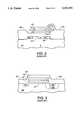
- FIG. 2is a cross section of a memory transistor implemented in E 2 PROM technology.
- FIG. 3is a cross section of a memory transistor implemented in FLASH memory technology.
- FIG. 4is a circuit schematic diagram of another electrically erasable programmable read-only memory architecture, in accordance with the invention.
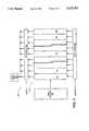
- a memory architecture 100is shown in FIG. 1.
- the memory 100is illustrative in that the method and apparatus for programming the memory 100 described herein are applicable to other memory architectures as well.
- another memory architectureis described in copending and commonly assigned U.S. Pat. application Ser. No. 07/896,772 entitled Electrical Erasable Programmable Read-Only Memory Array, naming Nagesh Challa as inventor and filed on even data herewith, which is incorporated herein by reference.
- Memory 100includes a number N of rows of memory cells, which generally are considered to be words of memory or, in a page-associative memory, a number N of pages of memory.
- Words 110, 120 and 130are shown.
- Each word of memory 100Comprises a number of memory cells.
- the word 110comprises data memory cells 111, 112, 113, 114, 115, 116, 117, and 118, and monitor Cells 174, 175 and 176.
- the second through Nth words, indicated generally at 120 and 130,are substantially identical to the word 110.
- Each of the data memory cells 111-118has a control terminal connected to a word line from port WL1 of row decoder 140, one controlled terminal connected to an associated bit line, and the other controlled terminal connected to an array ground line ASG.
- the memory cells 111-118 and 174-176are electrically erasable programmable read-only memory ("EEPROM") transistors, each having a control gate that is connected to a word line and functions as the control terminal, a drain that is connected to an associated bit line and functions as one of the controlled terminals, and a source that is connected to the array ground line ASG and functions as a second controlled terminal.
- the bit lines 191-198 associated with data transistors 111-118are connected to precharge and sense amplifier circuits 150 through respective column select transistors 151-158, which are controlled by column select signal CS.
- Circuits peripheral to the memory cell arrayinclude row decoder 140 having illustrative word select ports WL1 through WLN, where N is the number of words in the memory 100.
- Word select ports WL1-WLNare connected to word lines. With respect to word 110, for example, the word line 181 from the word select port WL1 is connected to the gates of memory transistors 111-118 and monitor memory transistors 174-176.
- the bit lines 191-198are connected to respective ports of a bit line precharge and sense amplifier circuit 150 through respective column select transistors 151-158, which are controlled by column select signal CS.
- the precharge and sense amplifier circuit 150is of any suitable conventional design.
- the bit lines 184, 185 and 186are connected to respective ports of a monitor circuit 170 through respective column select transistors 171, 172 and 173, which are controlled by sampling signal SAMP.
- Monitor circuit 170is a bit line precharge and sense amplifier circuit similar to the bit line precharge and sense amplifier circuit 150.
- the bit lines 191-198are also connected to respective ports of a data latches circuit 160 through respective column select transistors 161-168, which are controlled by load signal LOAD applied to their gates.
- the data latches circuit 160is of any suitable conventional design.
- the bit lines 184, 185 and 186also are connected to the data latches 160 through respective column select transistors 177, 178 and 179, which are controlled by the signal LOAD.
- Each of the memory cells of FIG. 1is a settable threshold device. Suitable devices are illustrated in FIGS. 2 and 3 are described in numerous publications, including the compendium by Cheming Hu, Non-volatile Semiconductor Memories, IEEE Publications, New York, 1991.
- the device of FIG. 2is a floating gate transistor fabricated in accordance with a conventional E 2 PROM process. Source 202 and drain 204 are formed in substrate 200, within an active area bounded by field oxide 206 and 208. A floating gate 214 is provided over the channel region between the source 202 and drain 204, and is insulated from the channel by a gate dielectric 210.
- a portion of the floating gate 214also overlays a portion of the drain 204, from which it is insulated by a thin tunnel dielectric 212.
- a control gate 218overlays the floating gate 214, and is insulated from the floating gate 214 by an interpoly dielectric 216.
- the device of FIG. 3is a floating gate transistor fabricated in accordance with a conventional flash memory process. Source 302 and a double diffused drain comprising sections 304 and 305 are formed in substrate 300, within an active area bounded by dielectric 306 and 308.
- a floating gate 314is provided both over the drain region 305 and over the channel region between the source 302 and drain region 305, and is insulated therefrom by a uniform dielectric layer 310, which comprises both gate and tunnel dielectric.
- a control gate 318overlays the floating gate 314, and is insulated from the floating gate 314 by an interpoly dielectric 316.
- the cell of FIG. 3shows a double diffused drain comprising regions 304 and 305, a suitable underlay can be achieved without double diffusion.
- the source region 302is shown with essentially no underlay, a source region having greater underlay may be fabricated if desired. Processes suitable for fabricating the transistors of FIGS. 2 and 3 are well known in the art.
- V tis variable, depending on the type and thickness of the dielectric (generally referred to as the "coupling ratio") through which the tunneling occurs, as well as the voltage applied and the nature and duration of application.
- a suitable coupling ratiois 0.65.
- the memory 100 of FIG. 1operates as follows, assuming use of the illustrative floating gate MOSFET described above with reference to FIG. 3.
- An illustrative set of voltagesis summarized in Table 1 below for both selected and deselected rows in erase, write, and read modes. It will be appreciated that these values are illustrative, and that similar operation can be achieved using different values of voltage and even a combination of positive and negative voltages, as described in the aforementioned copending Challa application, and even different types of adjustable threshold memory cells.
- Erase modeis defined as establishing a high V t in the memory transistors of the memory 100 so that they are nonconductive in the read mode. As nonconductive cells are sensed as logic one in the read mode, the result of an erase is to place logic ones into the memory cells associated with a selected row. Assume, for example, that erasure of memory transistors 111-118 in word 110 is desired. The control gates of transistors 111-118 and 174-176 are taken to a high voltage such as 20 volts. The control gates of transistors associated with deselected word lines are held at 0 volts.
- the drains of the memory transistors in the memory 100are held at 0 volts by loading logic one values into the data latches 430 and asserting signal LOAD positive.
- the sources of the memory transistors in the memory 100are held at zero volts.
- Transistors 111-118 and 174-176thereby have twenty volts applied across their respective control gates and drains with the control gates positive relative to the drains, so that electrons tunnel from the drain through the tunnel oxide to the floating gate to raise V t to greater than four volts.
- the memory transistors of the other words in the memory 100for example words 120 and 130, have zero volts applied across their respective control gates and drains, which is insufficient to disturb the data in these cells.
- the entire memory array of the memory 100can be erased, if desired, by taking all of the word lines WL1-WLN to 20 volts.
- Writing modeis defined as establishing a low V t in particular memory transistors of the memory 100 so that they are conductive in the read mode.
- a conductive memory transistoris sensed as a logic zero, so the memory transistors of memory 100 are “erased” into a logic one state, and selected transistors subsequently are “programmed” into a logic zero state.
- the binary value to be storedis latched by the data latches 160, and furnished to respective bit lines of the memory transistors 111-118.
- a logic oneis written into a memory transistor such as transistor 111, for example, by not disturbing the state of the transistor, which typically is logic one from the prior erase mode operation. Zero volts (or alternatively no voltage if the latch outputs are floating) is applied to the drain of the transistor 111. If word 110 is selected, transistor 111 has fifteen volts across its control gate and drain, with the control gates being negative relative to the drains, which is insufficient to cause tunneling. Hence, the logic one erased state is unchanged and V t remains greater than four volts. If word 110 is deselected, transistor 111 has zero volts across its control gate and drain, which is insufficient to cause tunneling. Hence, the logic one erased state is unchanged and V t remains greater than four volts.
- a logic zerois written to a memory transistor such as transistor 111, for example, by applying five volts to the drain of the transistor 111 through the data latches circuit 160. Note that a logic zero is always written to the monitor transistors 174, 175 and 176.
- Word 110is selected by bring word line WL1 to minus fifteen volts.
- Signal LOADis asserted positive, thereby turning on the column select transistors 161-168 and 177-179 to connect the bit lines 191-198 and 184-186 to the data latches 160.
- the ports of the data latches circuit 160 associated with the monitor transistors 174, 175 and 176are always at logic zero in write mode, when signal LOAD is asserted positive, so that the monitor transistors 174.
- Read modebegins by precharging all bit lines in the memory 100 to 1.5 volts.
- the common source ASGis at ground. If word 110 is being read, for example, selected word line WL1 is brought to 2.5 volts while the other word lines WL2-WLN are held at zero volts.
- Transistors in the selected word 110 having a high V t of about four volts or greaterdo not conduct, and the lack of current flow in the respective associated bit lines is read by sense amplifiers 150 as a logic one.
- Transistors in deselected words of the memory 100do not conduct, unless their V t is negative.
- Negative V tresults from a poorly controlled write to a memory transistor of a selected word, causing the transistor to be written into depletion. Because some read methods are not accurate when negative V t cells are present in the memory 100, the memory 100 includes a precharge and sense amplifier circuit and a number of extra memory monitor transistors distributed through the memory array for the purpose of detecting when transistors of the memory 100 are about to be written into depletion. Writing is stopped before any memory transistor in the memory 100 is written into depletion. Alternatively, if any memory transistor is written into depletion, the V t of the transistors in the selected word is incrementally raised until no transistor has a negative V t .
- each rowis provided a number of monitor transistors.
- word 110is provided with the three monitoring transistors 174-176, the drains of which are connected to monitor bit lines 184, 185 and 186.
- Monitor bit lines 184, 185 and 186are connected to the monitor circuit 170, which is a precharge and sense amplifier circuit similar to the precharge and sense amplifier circuit 150, through respective column select transistors 174, 175 and 176.
- Monitor bit lines 184, 185 and 186also are connected to associated latched in the data latches circuit 430, which contain a logic one in erase mode and a logic zero in write mode, through respective column load transistors 177, 178 and 179.
- the Write operationis performed as follows, assuming word 110 is being written. Data, including the monitor data of logic zero, is loaded into data latches 160. The memory 100 is placed into write mode, signal LOAD is asserted high to couple the data latches 160 to the bit lines 191-198 and 184-186, and port WL1 of the row decoder connected to word line 181 is brought to minus fifteen volts for a period sufficient to draw some charge off of the floating gates of the associated monitor transistors 174-176 and off of those memory transistors 111-118 that are being programmed to logic zero. The amount of charge preferably is insufficient to write these transistors into depletion.
- V t of the monitor transistors 174, 175 and 176 in word 110is sampled by asserting sampling select signal SAMP high to turn ON sampling select transistors 171, 172 and 173, bringing Word line 181 to a nonzero read Voltage of, for example, plus one volt, and sampling the current on bit lines 184, 185 and 186. If no current is sensed, word line 181 of the row decoder is again brought to minus fifteen volts for a period sufficient to draw some more charge off of the floating gates of the associated monitor transistors 174-176 and to draw some more charge off of those memory transistors 111-118 that are being programmed to logic zero.
- the periodis insufficient to write these transistors into depletion, and the monitor transistors 174, 175 and 176 are again sampled.
- the write-sample sequenceis repeated until current is sensed on one of the bit lines 184, 185 and 186.
- the word line 181is brought to zero volts and the bit lines 184, 185 and 186 are again sampled to confirm that none of the monitor transistors 174, 175 and 176 has been written into depletion.
- the memory transistors 111-118 and the monitor transistors 174-176can be slightly erased in a controllable manner so as to slightly raise their V t , and the bit lines 184, 185 and 186 are again sampled to determine whether any of the monitor transistors 174, 175 and 176 remains in depletion. If none remain in depletion, the memory 100 is successfully written. If one or more remain in depletion, the erase-sample cycle is repeated until none of the monitor transistors remain in depletion.
- the memory transistors 111-118 and the monitor transistors 174-176could be written in such a manner that they are likely to be overwritten, followed by a number of erase-sample cycles as described above to progressively increase their V t until none remain in depletion. At this point, the memory 100 is successfully written.
- the write perioddepends on the memory transistor parameters and other considerations. For example, one simple technique is to repeatedly apply the select voltage to the word line in 500 microsecond pulses until a successful write is detected. This technique could result in overerasure if significant charge is removed from the floating gates during the 500 microsecond period. Alternatively, the use of a progressively shorter period, decreasing, for example, to 200 microseconds and then to 100 microseconds, generally would avoid overerasure.
- the erase period to controllably raise negative V talso proceeds either in uniform increments or progressively decreasing increments. For example, a uniform increment of 100 microseconds is suitable.
- the memory 100is implemented in a conventional manner in silicon, using a grounded substrate. Alternatively, the memory 100 is implemented using a substrate that is held at a potential of, for example, about minus one volt. This allows the rows 110, 120 and 130 to be switched on and off quickly, without loss of access time. Moreover, a small negative bias reduces the diffusion capacitances and raises the nominal V t of all of the NMOS memory transistors, thereby helping to maintain the ability to read the selected cells in the memory array even if some of the cells degrade, or experience a drop in their V t , during the memory lifetime.
- the use of monitor bytes instead of monitor bitshas utility in a page organized memory architecture such as that shown in FIG. 4.
- the memory 400includes a row decoder 402 and a memory array 410.
- the memory array 410includes a number of columns represented by columns 411, 412, 413, 414 and 415. Each column is one byte wide, for example.
- Datais loaded in page mode through the data latches 430. Data is read by accessing individual bytes of data through byte select circuit 424, and each byte is sensed by byte-wide sense amplifier circuit 422. End columns 411 and 415 and center column 413 contain monitor bytes.
- the bits of the monitor bytesare first erased into logic one by loading logic ones into the associated latches of the data latches circuit 430 and selecting the appropriate word or words, and then programmed to logic zero by loading logic zeros into the associated latches of the data latches circuit 430 and selecting the appropriate word.
- the monitor bytes 411, 413 and 415are sampled without dedicated circuitry by being selected by byte select circuit 424 and sensed by the sense amplifiers 422.
Landscapes
- Read Only Memory (AREA)
Abstract
Description
TABLE 1 ______________________________________ MODE STATUS VWL VBL VASG Vt ______________________________________ ERASE Selected 20 0 0 >4 Deselected 0 0 0 Unchanged WRITE Selected -15 5 (binary 0) 0 See Text 0/F 0 >4 (binary 1) Deselected 0 5/0 0 Unchanged READ Selected 2.5 1.5 0 Deselected 0 F 0 ______________________________________
Claims (28)
Priority Applications (1)
| Application Number | Priority Date | Filing Date | Title |
|---|---|---|---|
| US07/897,215US5323351A (en) | 1992-06-10 | 1992-06-10 | Method and apparatus for programming electrical erasable programmable read-only memory arrays |
Applications Claiming Priority (1)
| Application Number | Priority Date | Filing Date | Title |
|---|---|---|---|
| US07/897,215US5323351A (en) | 1992-06-10 | 1992-06-10 | Method and apparatus for programming electrical erasable programmable read-only memory arrays |
Publications (1)
| Publication Number | Publication Date |
|---|---|
| US5323351Atrue US5323351A (en) | 1994-06-21 |
Family
ID=25407547
Family Applications (1)
| Application Number | Title | Priority Date | Filing Date |
|---|---|---|---|
| US07/897,215Expired - LifetimeUS5323351A (en) | 1992-06-10 | 1992-06-10 | Method and apparatus for programming electrical erasable programmable read-only memory arrays |
Country Status (1)
| Country | Link |
|---|---|
| US (1) | US5323351A (en) |
Cited By (27)
| Publication number | Priority date | Publication date | Assignee | Title |
|---|---|---|---|---|
| US5424997A (en)* | 1994-03-15 | 1995-06-13 | National Semiconductor Corporation | Non-volatile semiconductor memory having switching devices for segmentation of a memory page and a method thereof |
| US5557569A (en)* | 1993-10-12 | 1996-09-17 | Texas Instruments Incorporated | Low voltage flash EEPROM C-cell using fowler-nordheim tunneling |
| US5566109A (en)* | 1993-12-28 | 1996-10-15 | Mitsubishi Denki Kabushiki Kaisha | EEPROM, write control method for EEPROM, and IC card |
| WO1997048101A1 (en)* | 1996-06-14 | 1997-12-18 | Macronix International Co., Ltd. | Floating gate memory device with low current page buffer |
| US5748535A (en)* | 1994-10-26 | 1998-05-05 | Macronix International Co., Ltd. | Advanced program verify for page mode flash memory |
| US5754469A (en)* | 1996-06-14 | 1998-05-19 | Macronix International Co., Ltd. | Page mode floating gate memory device storing multiple bits per cell |
| US5784317A (en)* | 1995-12-27 | 1998-07-21 | Hyundai Electronics Industries Co., Ltd. | Flash memory device using an operational circuit for bit-by-bit verifying of programmed data in memory cells and method of programming the same |
| US5835414A (en)* | 1996-06-14 | 1998-11-10 | Macronix International Co., Ltd. | Page mode program, program verify, read and erase verify for floating gate memory device with low current page buffer |
| EP0728359A4 (en)* | 1994-09-13 | 1999-07-14 | Macronix Int Co Ltd | Flash eprom integrated circuit architecture |
| US5999448A (en)* | 1998-03-17 | 1999-12-07 | Fujitsu Limited | Nonvolatile semiconductor memory device and method of reproducing data of nonvolatile semiconductor memory device |
| US5999451A (en)* | 1998-07-13 | 1999-12-07 | Macronix International Co., Ltd. | Byte-wide write scheme for a page flash device |
| US6114724A (en)* | 1998-03-31 | 2000-09-05 | Cypress Semiconductor Corporation | Nonvolatile semiconductor memory cell with select gate |
| US20040042271A1 (en)* | 2002-08-27 | 2004-03-04 | Micron Technology, Inc. | Method and apparatus for erasing memory |
| US20040174739A1 (en)* | 2002-12-03 | 2004-09-09 | Hidenori Morimoto | Semiconductor memory device and data write method |
| US20040232995A1 (en)* | 2003-05-02 | 2004-11-25 | Silicon Laboratories Inc. | Dual loop architecture useful for a programmable clock source and clock multiplier applications |
| US20060067129A1 (en)* | 2004-08-26 | 2006-03-30 | Stmicroelectronics Sa | Method for reading electrically programmable and erasable memory cells, with bit line precharge-ahead |
| US20060244099A1 (en)* | 2004-05-06 | 2006-11-02 | Wlodek Kurjanowicz | Split-channel antifuse array architecture |
| US20070252196A1 (en)* | 2006-02-23 | 2007-11-01 | Jin-Young Kim | Vertical channel transistors and memory devices including vertical channel transistors |
| US20070268773A1 (en)* | 2006-05-18 | 2007-11-22 | Micron Technology, Inc. | Programming a non-volatile memory device |
| US20070285990A1 (en)* | 2006-06-10 | 2007-12-13 | Samsung Electronics Co., Ltd. | Semiconductor device and method for compensating voltage drop of a bit line |
| US20080117691A1 (en)* | 2006-11-17 | 2008-05-22 | Sharp Kabushiki Kaisha | Erasing circuit of nonvolatile semiconductor memory device |
| USRE41019E1 (en)* | 1993-09-21 | 2009-12-01 | Kabushiki Kaisha Toshiba | Multi-state EEPROM having write-verify control circuit |
| US20100244115A1 (en)* | 2004-05-06 | 2010-09-30 | Sidense Corporation | Anti-fuse memory cell |
| US20100259965A1 (en)* | 2004-05-06 | 2010-10-14 | Sidense Corp. | High speed otp sensing scheme |
| US8735297B2 (en) | 2004-05-06 | 2014-05-27 | Sidense Corporation | Reverse optical proximity correction method |
| US8767433B2 (en) | 2004-05-06 | 2014-07-01 | Sidense Corp. | Methods for testing unprogrammed OTP memory |
| US9123572B2 (en) | 2004-05-06 | 2015-09-01 | Sidense Corporation | Anti-fuse memory cell |
Citations (7)
| Publication number | Priority date | Publication date | Assignee | Title |
|---|---|---|---|---|
| US4460982A (en)* | 1982-05-20 | 1984-07-17 | Intel Corporation | Intelligent electrically programmable and electrically erasable ROM |
| US4698787A (en)* | 1984-11-21 | 1987-10-06 | Exel Microelectronics, Inc. | Single transistor electrically programmable memory device and method |
| US4996571A (en)* | 1988-07-08 | 1991-02-26 | Hitachi, Ltd. | Non-volatile semiconductor memory device erasing operation |
| US4996668A (en)* | 1988-08-09 | 1991-02-26 | Texas Instruments Incorporated | Erasable programmable memory |
| US5132935A (en)* | 1990-04-16 | 1992-07-21 | Ashmore Jr Benjamin H | Erasure of eeprom memory arrays to prevent over-erased cells |
| US5142496A (en)* | 1991-06-03 | 1992-08-25 | Advanced Micro Devices, Inc. | Method for measuring VT 's less than zero without applying negative voltages |
| US5163021A (en)* | 1989-04-13 | 1992-11-10 | Sundisk Corporation | Multi-state EEprom read and write circuits and techniques |
- 1992
- 1992-06-10USUS07/897,215patent/US5323351A/ennot_activeExpired - Lifetime
Patent Citations (7)
| Publication number | Priority date | Publication date | Assignee | Title |
|---|---|---|---|---|
| US4460982A (en)* | 1982-05-20 | 1984-07-17 | Intel Corporation | Intelligent electrically programmable and electrically erasable ROM |
| US4698787A (en)* | 1984-11-21 | 1987-10-06 | Exel Microelectronics, Inc. | Single transistor electrically programmable memory device and method |
| US4996571A (en)* | 1988-07-08 | 1991-02-26 | Hitachi, Ltd. | Non-volatile semiconductor memory device erasing operation |
| US4996668A (en)* | 1988-08-09 | 1991-02-26 | Texas Instruments Incorporated | Erasable programmable memory |
| US5163021A (en)* | 1989-04-13 | 1992-11-10 | Sundisk Corporation | Multi-state EEprom read and write circuits and techniques |
| US5132935A (en)* | 1990-04-16 | 1992-07-21 | Ashmore Jr Benjamin H | Erasure of eeprom memory arrays to prevent over-erased cells |
| US5142496A (en)* | 1991-06-03 | 1992-08-25 | Advanced Micro Devices, Inc. | Method for measuring VT 's less than zero without applying negative voltages |
Non-Patent Citations (3)
| Title |
|---|
| Robinson, "Endurance Brightens the Future of Flash," Technological Horizons, Nov. 1988, pp. 167-169. |
| Robinson, Endurance Brightens the Future of Flash, Technological Horizons, Nov. 1988, pp. 167 169.* |
| Wilson et al, Intel Flash Prices Rock Market, Electronic Engineering Times, Apr. 27, 1992, p. 1 and p. 93.* |
Cited By (43)
| Publication number | Priority date | Publication date | Assignee | Title |
|---|---|---|---|---|
| USRE41019E1 (en)* | 1993-09-21 | 2009-12-01 | Kabushiki Kaisha Toshiba | Multi-state EEPROM having write-verify control circuit |
| US5557569A (en)* | 1993-10-12 | 1996-09-17 | Texas Instruments Incorporated | Low voltage flash EEPROM C-cell using fowler-nordheim tunneling |
| US5566109A (en)* | 1993-12-28 | 1996-10-15 | Mitsubishi Denki Kabushiki Kaisha | EEPROM, write control method for EEPROM, and IC card |
| US5424997A (en)* | 1994-03-15 | 1995-06-13 | National Semiconductor Corporation | Non-volatile semiconductor memory having switching devices for segmentation of a memory page and a method thereof |
| EP0728359A4 (en)* | 1994-09-13 | 1999-07-14 | Macronix Int Co Ltd | Flash eprom integrated circuit architecture |
| EP1176602A1 (en)* | 1994-09-13 | 2002-01-30 | Macronix International Co., Ltd. | Flash EPROM integrated circuit architecture |
| US5748535A (en)* | 1994-10-26 | 1998-05-05 | Macronix International Co., Ltd. | Advanced program verify for page mode flash memory |
| US5784317A (en)* | 1995-12-27 | 1998-07-21 | Hyundai Electronics Industries Co., Ltd. | Flash memory device using an operational circuit for bit-by-bit verifying of programmed data in memory cells and method of programming the same |
| WO1997048101A1 (en)* | 1996-06-14 | 1997-12-18 | Macronix International Co., Ltd. | Floating gate memory device with low current page buffer |
| US5835414A (en)* | 1996-06-14 | 1998-11-10 | Macronix International Co., Ltd. | Page mode program, program verify, read and erase verify for floating gate memory device with low current page buffer |
| US5754469A (en)* | 1996-06-14 | 1998-05-19 | Macronix International Co., Ltd. | Page mode floating gate memory device storing multiple bits per cell |
| US5999448A (en)* | 1998-03-17 | 1999-12-07 | Fujitsu Limited | Nonvolatile semiconductor memory device and method of reproducing data of nonvolatile semiconductor memory device |
| US6114724A (en)* | 1998-03-31 | 2000-09-05 | Cypress Semiconductor Corporation | Nonvolatile semiconductor memory cell with select gate |
| US5999451A (en)* | 1998-07-13 | 1999-12-07 | Macronix International Co., Ltd. | Byte-wide write scheme for a page flash device |
| US6842380B2 (en)* | 2002-08-27 | 2005-01-11 | Micron Technology, Inc. | Method and apparatus for erasing memory |
| US20040042271A1 (en)* | 2002-08-27 | 2004-03-04 | Micron Technology, Inc. | Method and apparatus for erasing memory |
| US20040174739A1 (en)* | 2002-12-03 | 2004-09-09 | Hidenori Morimoto | Semiconductor memory device and data write method |
| EP1426975A3 (en)* | 2002-12-03 | 2006-03-22 | Sharp Kabushiki Kaisha | Semiconductor memory device and data write method |
| US7061790B2 (en) | 2002-12-03 | 2006-06-13 | Sharp Kabushiki Kaisha | Semiconductor memory device and data write method |
| US20040232995A1 (en)* | 2003-05-02 | 2004-11-25 | Silicon Laboratories Inc. | Dual loop architecture useful for a programmable clock source and clock multiplier applications |
| US8735297B2 (en) | 2004-05-06 | 2014-05-27 | Sidense Corporation | Reverse optical proximity correction method |
| US20080246098A1 (en)* | 2004-05-06 | 2008-10-09 | Sidense Corp. | Split-channel antifuse array architecture |
| US9123572B2 (en) | 2004-05-06 | 2015-09-01 | Sidense Corporation | Anti-fuse memory cell |
| US8767433B2 (en) | 2004-05-06 | 2014-07-01 | Sidense Corp. | Methods for testing unprogrammed OTP memory |
| US8026574B2 (en) | 2004-05-06 | 2011-09-27 | Sidense Corporation | Anti-fuse memory cell |
| US7402855B2 (en)* | 2004-05-06 | 2008-07-22 | Sidense Corp. | Split-channel antifuse array architecture |
| US8313987B2 (en) | 2004-05-06 | 2012-11-20 | Sidense Corp. | Anti-fuse memory cell |
| US20060244099A1 (en)* | 2004-05-06 | 2006-11-02 | Wlodek Kurjanowicz | Split-channel antifuse array architecture |
| US8283751B2 (en) | 2004-05-06 | 2012-10-09 | Sidense Corp. | Split-channel antifuse array architecture |
| US20100259965A1 (en)* | 2004-05-06 | 2010-10-14 | Sidense Corp. | High speed otp sensing scheme |
| US20100244115A1 (en)* | 2004-05-06 | 2010-09-30 | Sidense Corporation | Anti-fuse memory cell |
| US8130532B2 (en) | 2004-05-06 | 2012-03-06 | Sidense Corp. | High speed OTP sensing scheme |
| US20060067129A1 (en)* | 2004-08-26 | 2006-03-30 | Stmicroelectronics Sa | Method for reading electrically programmable and erasable memory cells, with bit line precharge-ahead |
| US7529145B2 (en)* | 2004-08-26 | 2009-05-05 | Stmicroelectronics Sa | Method for reading electrically programmable and erasable memory cells, with bit line precharge-ahead |
| US20070252196A1 (en)* | 2006-02-23 | 2007-11-01 | Jin-Young Kim | Vertical channel transistors and memory devices including vertical channel transistors |
| US7977736B2 (en)* | 2006-02-23 | 2011-07-12 | Samsung Electronics Co., Ltd. | Vertical channel transistors and memory devices including vertical channel transistors |
| CN101150132B (en)* | 2006-02-23 | 2011-12-07 | 三星电子株式会社 | Vertical channel transistors and memory devices including vertical channel transistors |
| US7663930B2 (en) | 2006-05-18 | 2010-02-16 | Micron Technology, Inc. | Programming a non-volatile memory device |
| US20080266972A1 (en)* | 2006-05-18 | 2008-10-30 | Seiichi Aritome | Programming a non-volatile memory device |
| US7411832B2 (en) | 2006-05-18 | 2008-08-12 | Micron Technology, Inc. | Programming a non-volatile memory device |
| US20070268773A1 (en)* | 2006-05-18 | 2007-11-22 | Micron Technology, Inc. | Programming a non-volatile memory device |
| US20070285990A1 (en)* | 2006-06-10 | 2007-12-13 | Samsung Electronics Co., Ltd. | Semiconductor device and method for compensating voltage drop of a bit line |
| US20080117691A1 (en)* | 2006-11-17 | 2008-05-22 | Sharp Kabushiki Kaisha | Erasing circuit of nonvolatile semiconductor memory device |
Similar Documents
| Publication | Publication Date | Title |
|---|---|---|
| US5323351A (en) | Method and apparatus for programming electrical erasable programmable read-only memory arrays | |
| US5414658A (en) | Electrically erasable programmable read-only memory array | |
| US5838617A (en) | Method for changing electrically programmable read-only memory devices | |
| US4375087A (en) | Electrically erasable programmable read only memory | |
| US6160739A (en) | Non-volatile memories with improved endurance and extended lifetime | |
| US5909393A (en) | Method and apparatus for reading analog values stored in floating gate NAND structures | |
| US6205059B1 (en) | Method for erasing flash electrically erasable programmable read-only memory (EEPROM) | |
| US4266283A (en) | Electrically alterable read-mostly memory | |
| US6108240A (en) | Implementation of EEPROM using intermediate gate voltage to avoid disturb conditions | |
| US5790456A (en) | Multiple bits-per-cell flash EEPROM memory cells with wide program and erase Vt window | |
| US5357476A (en) | Apparatus and method for erasing a flash EEPROM | |
| US6909639B2 (en) | Nonvolatile memory having bit line discharge, and method of operation thereof | |
| US6240016B1 (en) | Method to reduce read gate disturb for flash EEPROM application | |
| US5521867A (en) | Adjustable threshold voltage conversion circuit | |
| US6438037B1 (en) | Threshold voltage compacting for non-volatile semiconductor memory designs | |
| EP0503756B1 (en) | Method of programming flash EEPROM cell arrays | |
| KR20050008725A (en) | Method of erasing a flashing memory using a pre-reasing step | |
| JPS5894196A (en) | Memory device | |
| US6584016B2 (en) | Non-volatile memory architecture and method of operation | |
| US5428578A (en) | Biasing circuit and method to achieve compaction and self-limiting erase in flash EEPROMs | |
| US5424991A (en) | Floating gate nonvolatile memory with uniformly erased threshold voltage | |
| US5805499A (en) | Channel hot-carrier page write for NAND applications | |
| US5220528A (en) | Compensation circuit for leakage in flash EPROM | |
| US6363014B1 (en) | Low column leakage NOR flash array-single cell implementation | |
| EP0108681A2 (en) | Bit erasable electrically erasable programmable read only memory |
Legal Events
| Date | Code | Title | Description |
|---|---|---|---|
| AS | Assignment | Owner name:NEXCOM TECHNOLOGY, INC., CALIFORNIA Free format text:ASSIGNMENT OF ASSIGNORS INTEREST.;ASSIGNOR:CHALLA, NAGESH;REEL/FRAME:006241/0334 Effective date:19920804 | |
| STCF | Information on status: patent grant | Free format text:PATENTED CASE | |
| FPAY | Fee payment | Year of fee payment:4 | |
| AS | Assignment | Owner name:INTEGRATED SILICON SOLUTION, INC., CALIFORNIA Free format text:ASSIGNMENT OF ASSIGNORS INTEREST;ASSIGNOR:NEXCOM TECHNOLOGY, INC.;REEL/FRAME:008933/0038 Effective date:19980115 | |
| AS | Assignment | Owner name:NEXFLASH TECHNOLOGIES, INC., CALIFORNIA Free format text:ASSIGNMENT OF ASSIGNORS INTEREST;ASSIGNOR:INTEGRATED SILICON SOLUTION, INC.;REEL/FRAME:009857/0495 Effective date:19990303 | |
| FEPP | Fee payment procedure | Free format text:PAYOR NUMBER ASSIGNED (ORIGINAL EVENT CODE: ASPN); ENTITY STATUS OF PATENT OWNER: LARGE ENTITY | |
| FPAY | Fee payment | Year of fee payment:8 | |
| FPAY | Fee payment | Year of fee payment:12 | |
| AS | Assignment | Owner name:WINBOND ELECTRONICS CORPORATION, TAIWAN Free format text:ASSIGNMENT OF ASSIGNORS INTEREST;ASSIGNOR:NEXFLASH TECHNOLOGIES, INC.;REEL/FRAME:017297/0984 Effective date:20060222 |