US5323060A - Multichip module having a stacked chip arrangement - Google Patents
Multichip module having a stacked chip arrangementDownload PDFInfo
- Publication number
- US5323060A US5323060AUS08/071,580US7158093AUS5323060AUS 5323060 AUS5323060 AUS 5323060AUS 7158093 AUS7158093 AUS 7158093AUS 5323060 AUS5323060 AUS 5323060A
- Authority
- US
- United States
- Prior art keywords
- chip
- bonding
- multichip module
- central area
- face
- Prior art date
- Legal status (The legal status is an assumption and is not a legal conclusion. Google has not performed a legal analysis and makes no representation as to the accuracy of the status listed.)
- Expired - Lifetime
Links
Images


Classifications
- H—ELECTRICITY
- H01—ELECTRIC ELEMENTS
- H01L—SEMICONDUCTOR DEVICES NOT COVERED BY CLASS H10
- H01L24/00—Arrangements for connecting or disconnecting semiconductor or solid-state bodies; Methods or apparatus related thereto
- H01L24/80—Methods for connecting semiconductor or other solid state bodies using means for bonding being attached to, or being formed on, the surface to be connected
- H01L24/85—Methods for connecting semiconductor or other solid state bodies using means for bonding being attached to, or being formed on, the surface to be connected using a wire connector
- H—ELECTRICITY
- H01—ELECTRIC ELEMENTS
- H01L—SEMICONDUCTOR DEVICES NOT COVERED BY CLASS H10
- H01L24/00—Arrangements for connecting or disconnecting semiconductor or solid-state bodies; Methods or apparatus related thereto
- H01L24/01—Means for bonding being attached to, or being formed on, the surface to be connected, e.g. chip-to-package, die-attach, "first-level" interconnects; Manufacturing methods related thereto
- H01L24/26—Layer connectors, e.g. plate connectors, solder or adhesive layers; Manufacturing methods related thereto
- H01L24/31—Structure, shape, material or disposition of the layer connectors after the connecting process
- H01L24/32—Structure, shape, material or disposition of the layer connectors after the connecting process of an individual layer connector
- H—ELECTRICITY
- H01—ELECTRIC ELEMENTS
- H01L—SEMICONDUCTOR DEVICES NOT COVERED BY CLASS H10
- H01L24/00—Arrangements for connecting or disconnecting semiconductor or solid-state bodies; Methods or apparatus related thereto
- H01L24/01—Means for bonding being attached to, or being formed on, the surface to be connected, e.g. chip-to-package, die-attach, "first-level" interconnects; Manufacturing methods related thereto
- H01L24/42—Wire connectors; Manufacturing methods related thereto
- H01L24/47—Structure, shape, material or disposition of the wire connectors after the connecting process
- H01L24/48—Structure, shape, material or disposition of the wire connectors after the connecting process of an individual wire connector
- H—ELECTRICITY
- H01—ELECTRIC ELEMENTS
- H01L—SEMICONDUCTOR DEVICES NOT COVERED BY CLASS H10
- H01L24/00—Arrangements for connecting or disconnecting semiconductor or solid-state bodies; Methods or apparatus related thereto
- H01L24/01—Means for bonding being attached to, or being formed on, the surface to be connected, e.g. chip-to-package, die-attach, "first-level" interconnects; Manufacturing methods related thereto
- H01L24/42—Wire connectors; Manufacturing methods related thereto
- H01L24/47—Structure, shape, material or disposition of the wire connectors after the connecting process
- H01L24/49—Structure, shape, material or disposition of the wire connectors after the connecting process of a plurality of wire connectors
- H—ELECTRICITY
- H01—ELECTRIC ELEMENTS
- H01L—SEMICONDUCTOR DEVICES NOT COVERED BY CLASS H10
- H01L24/00—Arrangements for connecting or disconnecting semiconductor or solid-state bodies; Methods or apparatus related thereto
- H01L24/80—Methods for connecting semiconductor or other solid state bodies using means for bonding being attached to, or being formed on, the surface to be connected
- H01L24/83—Methods for connecting semiconductor or other solid state bodies using means for bonding being attached to, or being formed on, the surface to be connected using a layer connector
- H—ELECTRICITY
- H01—ELECTRIC ELEMENTS
- H01L—SEMICONDUCTOR DEVICES NOT COVERED BY CLASS H10
- H01L25/00—Assemblies consisting of a plurality of semiconductor or other solid state devices
- H01L25/03—Assemblies consisting of a plurality of semiconductor or other solid state devices all the devices being of a type provided for in a single subclass of subclasses H10B, H10D, H10F, H10H, H10K or H10N, e.g. assemblies of rectifier diodes
- H01L25/04—Assemblies consisting of a plurality of semiconductor or other solid state devices all the devices being of a type provided for in a single subclass of subclasses H10B, H10D, H10F, H10H, H10K or H10N, e.g. assemblies of rectifier diodes the devices not having separate containers
- H01L25/065—Assemblies consisting of a plurality of semiconductor or other solid state devices all the devices being of a type provided for in a single subclass of subclasses H10B, H10D, H10F, H10H, H10K or H10N, e.g. assemblies of rectifier diodes the devices not having separate containers the devices being of a type provided for in group H10D89/00
- H01L25/0652—Assemblies consisting of a plurality of semiconductor or other solid state devices all the devices being of a type provided for in a single subclass of subclasses H10B, H10D, H10F, H10H, H10K or H10N, e.g. assemblies of rectifier diodes the devices not having separate containers the devices being of a type provided for in group H10D89/00 the devices being arranged next and on each other, i.e. mixed assemblies
- H—ELECTRICITY
- H01—ELECTRIC ELEMENTS
- H01L—SEMICONDUCTOR DEVICES NOT COVERED BY CLASS H10
- H01L2224/00—Indexing scheme for arrangements for connecting or disconnecting semiconductor or solid-state bodies and methods related thereto as covered by H01L24/00
- H01L2224/01—Means for bonding being attached to, or being formed on, the surface to be connected, e.g. chip-to-package, die-attach, "first-level" interconnects; Manufacturing methods related thereto
- H01L2224/26—Layer connectors, e.g. plate connectors, solder or adhesive layers; Manufacturing methods related thereto
- H01L2224/28—Structure, shape, material or disposition of the layer connectors prior to the connecting process
- H01L2224/29—Structure, shape, material or disposition of the layer connectors prior to the connecting process of an individual layer connector
- H01L2224/29001—Core members of the layer connector
- H01L2224/29099—Material
- H01L2224/2919—Material with a principal constituent of the material being a polymer, e.g. polyester, phenolic based polymer, epoxy
- H—ELECTRICITY
- H01—ELECTRIC ELEMENTS
- H01L—SEMICONDUCTOR DEVICES NOT COVERED BY CLASS H10
- H01L2224/00—Indexing scheme for arrangements for connecting or disconnecting semiconductor or solid-state bodies and methods related thereto as covered by H01L24/00
- H01L2224/01—Means for bonding being attached to, or being formed on, the surface to be connected, e.g. chip-to-package, die-attach, "first-level" interconnects; Manufacturing methods related thereto
- H01L2224/26—Layer connectors, e.g. plate connectors, solder or adhesive layers; Manufacturing methods related thereto
- H01L2224/31—Structure, shape, material or disposition of the layer connectors after the connecting process
- H01L2224/32—Structure, shape, material or disposition of the layer connectors after the connecting process of an individual layer connector
- H01L2224/3201—Structure
- H01L2224/32012—Structure relative to the bonding area, e.g. bond pad
- H01L2224/32014—Structure relative to the bonding area, e.g. bond pad the layer connector being smaller than the bonding area, e.g. bond pad
- H—ELECTRICITY
- H01—ELECTRIC ELEMENTS
- H01L—SEMICONDUCTOR DEVICES NOT COVERED BY CLASS H10
- H01L2224/00—Indexing scheme for arrangements for connecting or disconnecting semiconductor or solid-state bodies and methods related thereto as covered by H01L24/00
- H01L2224/01—Means for bonding being attached to, or being formed on, the surface to be connected, e.g. chip-to-package, die-attach, "first-level" interconnects; Manufacturing methods related thereto
- H01L2224/26—Layer connectors, e.g. plate connectors, solder or adhesive layers; Manufacturing methods related thereto
- H01L2224/31—Structure, shape, material or disposition of the layer connectors after the connecting process
- H01L2224/32—Structure, shape, material or disposition of the layer connectors after the connecting process of an individual layer connector
- H01L2224/321—Disposition
- H01L2224/32135—Disposition the layer connector connecting between different semiconductor or solid-state bodies, i.e. chip-to-chip
- H01L2224/32145—Disposition the layer connector connecting between different semiconductor or solid-state bodies, i.e. chip-to-chip the bodies being stacked
- H—ELECTRICITY
- H01—ELECTRIC ELEMENTS
- H01L—SEMICONDUCTOR DEVICES NOT COVERED BY CLASS H10
- H01L2224/00—Indexing scheme for arrangements for connecting or disconnecting semiconductor or solid-state bodies and methods related thereto as covered by H01L24/00
- H01L2224/01—Means for bonding being attached to, or being formed on, the surface to be connected, e.g. chip-to-package, die-attach, "first-level" interconnects; Manufacturing methods related thereto
- H01L2224/42—Wire connectors; Manufacturing methods related thereto
- H01L2224/47—Structure, shape, material or disposition of the wire connectors after the connecting process
- H01L2224/48—Structure, shape, material or disposition of the wire connectors after the connecting process of an individual wire connector
- H01L2224/4805—Shape
- H01L2224/4809—Loop shape
- H01L2224/48091—Arched
- H—ELECTRICITY
- H01—ELECTRIC ELEMENTS
- H01L—SEMICONDUCTOR DEVICES NOT COVERED BY CLASS H10
- H01L2224/00—Indexing scheme for arrangements for connecting or disconnecting semiconductor or solid-state bodies and methods related thereto as covered by H01L24/00
- H01L2224/01—Means for bonding being attached to, or being formed on, the surface to be connected, e.g. chip-to-package, die-attach, "first-level" interconnects; Manufacturing methods related thereto
- H01L2224/42—Wire connectors; Manufacturing methods related thereto
- H01L2224/47—Structure, shape, material or disposition of the wire connectors after the connecting process
- H01L2224/48—Structure, shape, material or disposition of the wire connectors after the connecting process of an individual wire connector
- H01L2224/4805—Shape
- H01L2224/4809—Loop shape
- H01L2224/48095—Kinked
- H—ELECTRICITY
- H01—ELECTRIC ELEMENTS
- H01L—SEMICONDUCTOR DEVICES NOT COVERED BY CLASS H10
- H01L2224/00—Indexing scheme for arrangements for connecting or disconnecting semiconductor or solid-state bodies and methods related thereto as covered by H01L24/00
- H01L2224/01—Means for bonding being attached to, or being formed on, the surface to be connected, e.g. chip-to-package, die-attach, "first-level" interconnects; Manufacturing methods related thereto
- H01L2224/42—Wire connectors; Manufacturing methods related thereto
- H01L2224/47—Structure, shape, material or disposition of the wire connectors after the connecting process
- H01L2224/48—Structure, shape, material or disposition of the wire connectors after the connecting process of an individual wire connector
- H01L2224/481—Disposition
- H01L2224/4813—Connecting within a semiconductor or solid-state body, i.e. fly wire, bridge wire
- H—ELECTRICITY
- H01—ELECTRIC ELEMENTS
- H01L—SEMICONDUCTOR DEVICES NOT COVERED BY CLASS H10
- H01L2224/00—Indexing scheme for arrangements for connecting or disconnecting semiconductor or solid-state bodies and methods related thereto as covered by H01L24/00
- H01L2224/01—Means for bonding being attached to, or being formed on, the surface to be connected, e.g. chip-to-package, die-attach, "first-level" interconnects; Manufacturing methods related thereto
- H01L2224/42—Wire connectors; Manufacturing methods related thereto
- H01L2224/47—Structure, shape, material or disposition of the wire connectors after the connecting process
- H01L2224/48—Structure, shape, material or disposition of the wire connectors after the connecting process of an individual wire connector
- H01L2224/481—Disposition
- H01L2224/48135—Connecting between different semiconductor or solid-state bodies, i.e. chip-to-chip
- H01L2224/48137—Connecting between different semiconductor or solid-state bodies, i.e. chip-to-chip the bodies being arranged next to each other, e.g. on a common substrate
- H—ELECTRICITY
- H01—ELECTRIC ELEMENTS
- H01L—SEMICONDUCTOR DEVICES NOT COVERED BY CLASS H10
- H01L2224/00—Indexing scheme for arrangements for connecting or disconnecting semiconductor or solid-state bodies and methods related thereto as covered by H01L24/00
- H01L2224/01—Means for bonding being attached to, or being formed on, the surface to be connected, e.g. chip-to-package, die-attach, "first-level" interconnects; Manufacturing methods related thereto
- H01L2224/42—Wire connectors; Manufacturing methods related thereto
- H01L2224/47—Structure, shape, material or disposition of the wire connectors after the connecting process
- H01L2224/48—Structure, shape, material or disposition of the wire connectors after the connecting process of an individual wire connector
- H01L2224/481—Disposition
- H01L2224/48151—Connecting between a semiconductor or solid-state body and an item not being a semiconductor or solid-state body, e.g. chip-to-substrate, chip-to-passive
- H01L2224/48153—Connecting between a semiconductor or solid-state body and an item not being a semiconductor or solid-state body, e.g. chip-to-substrate, chip-to-passive the body and the item being arranged next to each other, e.g. on a common substrate
- H01L2224/48175—Connecting between a semiconductor or solid-state body and an item not being a semiconductor or solid-state body, e.g. chip-to-substrate, chip-to-passive the body and the item being arranged next to each other, e.g. on a common substrate the item being metallic
- H—ELECTRICITY
- H01—ELECTRIC ELEMENTS
- H01L—SEMICONDUCTOR DEVICES NOT COVERED BY CLASS H10
- H01L2224/00—Indexing scheme for arrangements for connecting or disconnecting semiconductor or solid-state bodies and methods related thereto as covered by H01L24/00
- H01L2224/01—Means for bonding being attached to, or being formed on, the surface to be connected, e.g. chip-to-package, die-attach, "first-level" interconnects; Manufacturing methods related thereto
- H01L2224/42—Wire connectors; Manufacturing methods related thereto
- H01L2224/47—Structure, shape, material or disposition of the wire connectors after the connecting process
- H01L2224/48—Structure, shape, material or disposition of the wire connectors after the connecting process of an individual wire connector
- H01L2224/481—Disposition
- H01L2224/48151—Connecting between a semiconductor or solid-state body and an item not being a semiconductor or solid-state body, e.g. chip-to-substrate, chip-to-passive
- H01L2224/48221—Connecting between a semiconductor or solid-state body and an item not being a semiconductor or solid-state body, e.g. chip-to-substrate, chip-to-passive the body and the item being stacked
- H01L2224/48225—Connecting between a semiconductor or solid-state body and an item not being a semiconductor or solid-state body, e.g. chip-to-substrate, chip-to-passive the body and the item being stacked the item being non-metallic, e.g. insulating substrate with or without metallisation
- H01L2224/48227—Connecting between a semiconductor or solid-state body and an item not being a semiconductor or solid-state body, e.g. chip-to-substrate, chip-to-passive the body and the item being stacked the item being non-metallic, e.g. insulating substrate with or without metallisation connecting the wire to a bond pad of the item
- H—ELECTRICITY
- H01—ELECTRIC ELEMENTS
- H01L—SEMICONDUCTOR DEVICES NOT COVERED BY CLASS H10
- H01L2224/00—Indexing scheme for arrangements for connecting or disconnecting semiconductor or solid-state bodies and methods related thereto as covered by H01L24/00
- H01L2224/01—Means for bonding being attached to, or being formed on, the surface to be connected, e.g. chip-to-package, die-attach, "first-level" interconnects; Manufacturing methods related thereto
- H01L2224/42—Wire connectors; Manufacturing methods related thereto
- H01L2224/47—Structure, shape, material or disposition of the wire connectors after the connecting process
- H01L2224/48—Structure, shape, material or disposition of the wire connectors after the connecting process of an individual wire connector
- H01L2224/484—Connecting portions
- H01L2224/48463—Connecting portions the connecting portion on the bonding area of the semiconductor or solid-state body being a ball bond
- H01L2224/48465—Connecting portions the connecting portion on the bonding area of the semiconductor or solid-state body being a ball bond the other connecting portion not on the bonding area being a wedge bond, i.e. ball-to-wedge, regular stitch
- H—ELECTRICITY
- H01—ELECTRIC ELEMENTS
- H01L—SEMICONDUCTOR DEVICES NOT COVERED BY CLASS H10
- H01L2224/00—Indexing scheme for arrangements for connecting or disconnecting semiconductor or solid-state bodies and methods related thereto as covered by H01L24/00
- H01L2224/01—Means for bonding being attached to, or being formed on, the surface to be connected, e.g. chip-to-package, die-attach, "first-level" interconnects; Manufacturing methods related thereto
- H01L2224/42—Wire connectors; Manufacturing methods related thereto
- H01L2224/47—Structure, shape, material or disposition of the wire connectors after the connecting process
- H01L2224/49—Structure, shape, material or disposition of the wire connectors after the connecting process of a plurality of wire connectors
- H01L2224/491—Disposition
- H01L2224/4912—Layout
- H01L2224/49175—Parallel arrangements
- H—ELECTRICITY
- H01—ELECTRIC ELEMENTS
- H01L—SEMICONDUCTOR DEVICES NOT COVERED BY CLASS H10
- H01L2224/00—Indexing scheme for arrangements for connecting or disconnecting semiconductor or solid-state bodies and methods related thereto as covered by H01L24/00
- H01L2224/01—Means for bonding being attached to, or being formed on, the surface to be connected, e.g. chip-to-package, die-attach, "first-level" interconnects; Manufacturing methods related thereto
- H01L2224/42—Wire connectors; Manufacturing methods related thereto
- H01L2224/47—Structure, shape, material or disposition of the wire connectors after the connecting process
- H01L2224/49—Structure, shape, material or disposition of the wire connectors after the connecting process of a plurality of wire connectors
- H01L2224/494—Connecting portions
- H01L2224/4943—Connecting portions the connecting portions being staggered
- H01L2224/49433—Connecting portions the connecting portions being staggered outside the semiconductor or solid-state body
- H—ELECTRICITY
- H01—ELECTRIC ELEMENTS
- H01L—SEMICONDUCTOR DEVICES NOT COVERED BY CLASS H10
- H01L2224/00—Indexing scheme for arrangements for connecting or disconnecting semiconductor or solid-state bodies and methods related thereto as covered by H01L24/00
- H01L2224/73—Means for bonding being of different types provided for in two or more of groups H01L2224/10, H01L2224/18, H01L2224/26, H01L2224/34, H01L2224/42, H01L2224/50, H01L2224/63, H01L2224/71
- H01L2224/732—Location after the connecting process
- H01L2224/73251—Location after the connecting process on different surfaces
- H01L2224/73265—Layer and wire connectors
- H—ELECTRICITY
- H01—ELECTRIC ELEMENTS
- H01L—SEMICONDUCTOR DEVICES NOT COVERED BY CLASS H10
- H01L2224/00—Indexing scheme for arrangements for connecting or disconnecting semiconductor or solid-state bodies and methods related thereto as covered by H01L24/00
- H01L2224/80—Methods for connecting semiconductor or other solid state bodies using means for bonding being attached to, or being formed on, the surface to be connected
- H01L2224/83—Methods for connecting semiconductor or other solid state bodies using means for bonding being attached to, or being formed on, the surface to be connected using a layer connector
- H01L2224/8319—Arrangement of the layer connectors prior to mounting
- H—ELECTRICITY
- H01—ELECTRIC ELEMENTS
- H01L—SEMICONDUCTOR DEVICES NOT COVERED BY CLASS H10
- H01L2224/00—Indexing scheme for arrangements for connecting or disconnecting semiconductor or solid-state bodies and methods related thereto as covered by H01L24/00
- H01L2224/80—Methods for connecting semiconductor or other solid state bodies using means for bonding being attached to, or being formed on, the surface to be connected
- H01L2224/83—Methods for connecting semiconductor or other solid state bodies using means for bonding being attached to, or being formed on, the surface to be connected using a layer connector
- H01L2224/838—Bonding techniques
- H01L2224/8385—Bonding techniques using a polymer adhesive, e.g. an adhesive based on silicone, epoxy, polyimide, polyester
- H—ELECTRICITY
- H01—ELECTRIC ELEMENTS
- H01L—SEMICONDUCTOR DEVICES NOT COVERED BY CLASS H10
- H01L24/00—Arrangements for connecting or disconnecting semiconductor or solid-state bodies; Methods or apparatus related thereto
- H01L24/73—Means for bonding being of different types provided for in two or more of groups H01L24/10, H01L24/18, H01L24/26, H01L24/34, H01L24/42, H01L24/50, H01L24/63, H01L24/71
- H—ELECTRICITY
- H01—ELECTRIC ELEMENTS
- H01L—SEMICONDUCTOR DEVICES NOT COVERED BY CLASS H10
- H01L2924/00—Indexing scheme for arrangements or methods for connecting or disconnecting semiconductor or solid-state bodies as covered by H01L24/00
- H01L2924/0001—Technical content checked by a classifier
- H01L2924/00014—Technical content checked by a classifier the subject-matter covered by the group, the symbol of which is combined with the symbol of this group, being disclosed without further technical details
- H—ELECTRICITY
- H01—ELECTRIC ELEMENTS
- H01L—SEMICONDUCTOR DEVICES NOT COVERED BY CLASS H10
- H01L2924/00—Indexing scheme for arrangements or methods for connecting or disconnecting semiconductor or solid-state bodies as covered by H01L24/00
- H01L2924/01—Chemical elements
- H01L2924/01005—Boron [B]
- H—ELECTRICITY
- H01—ELECTRIC ELEMENTS
- H01L—SEMICONDUCTOR DEVICES NOT COVERED BY CLASS H10
- H01L2924/00—Indexing scheme for arrangements or methods for connecting or disconnecting semiconductor or solid-state bodies as covered by H01L24/00
- H01L2924/01—Chemical elements
- H01L2924/01006—Carbon [C]
- H—ELECTRICITY
- H01—ELECTRIC ELEMENTS
- H01L—SEMICONDUCTOR DEVICES NOT COVERED BY CLASS H10
- H01L2924/00—Indexing scheme for arrangements or methods for connecting or disconnecting semiconductor or solid-state bodies as covered by H01L24/00
- H01L2924/06—Polymers
- H01L2924/0665—Epoxy resin
- H—ELECTRICITY
- H01—ELECTRIC ELEMENTS
- H01L—SEMICONDUCTOR DEVICES NOT COVERED BY CLASS H10
- H01L2924/00—Indexing scheme for arrangements or methods for connecting or disconnecting semiconductor or solid-state bodies as covered by H01L24/00
- H01L2924/06—Polymers
- H01L2924/078—Adhesive characteristics other than chemical
- H01L2924/07802—Adhesive characteristics other than chemical not being an ohmic electrical conductor
- H—ELECTRICITY
- H01—ELECTRIC ELEMENTS
- H01L—SEMICONDUCTOR DEVICES NOT COVERED BY CLASS H10
- H01L2924/00—Indexing scheme for arrangements or methods for connecting or disconnecting semiconductor or solid-state bodies as covered by H01L24/00
- H01L2924/10—Details of semiconductor or other solid state devices to be connected
- H01L2924/11—Device type
- H01L2924/14—Integrated circuits
- H—ELECTRICITY
- H01—ELECTRIC ELEMENTS
- H01L—SEMICONDUCTOR DEVICES NOT COVERED BY CLASS H10
- H01L2924/00—Indexing scheme for arrangements or methods for connecting or disconnecting semiconductor or solid-state bodies as covered by H01L24/00
- H01L2924/19—Details of hybrid assemblies other than the semiconductor or other solid state devices to be connected
- H01L2924/1901—Structure
- H01L2924/1904—Component type
- H01L2924/19043—Component type being a resistor
- H—ELECTRICITY
- H01—ELECTRIC ELEMENTS
- H01L—SEMICONDUCTOR DEVICES NOT COVERED BY CLASS H10
- H01L2924/00—Indexing scheme for arrangements or methods for connecting or disconnecting semiconductor or solid-state bodies as covered by H01L24/00
- H01L2924/19—Details of hybrid assemblies other than the semiconductor or other solid state devices to be connected
- H01L2924/191—Disposition
- H01L2924/19101—Disposition of discrete passive components
- H01L2924/19105—Disposition of discrete passive components in a side-by-side arrangement on a common die mounting substrate
- H—ELECTRICITY
- H01—ELECTRIC ELEMENTS
- H01L—SEMICONDUCTOR DEVICES NOT COVERED BY CLASS H10
- H01L2924/00—Indexing scheme for arrangements or methods for connecting or disconnecting semiconductor or solid-state bodies as covered by H01L24/00
- H01L2924/19—Details of hybrid assemblies other than the semiconductor or other solid state devices to be connected
- H01L2924/191—Disposition
- H01L2924/19101—Disposition of discrete passive components
- H01L2924/19107—Disposition of discrete passive components off-chip wires
Definitions
- This inventionrelates specifically to wire bonding of multichip modules to multichip module substrates.
- multichip moduleThis invention concerns the specific art area of multichip modules.
- Multichip modulescan be fabricated faster and more cheaply than by designing new substrate integrated circuitry.
- Multichip module technologyis advantageous because of the density increase. With increased density comes equivalent improvements in signal propagation speed and overall device weight unmatched by other means.
- Current multichip module constructiontypically consists of a printed circuit board substrate to which a series of integrated circuit components are directly adhered.
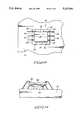
- FIG. 1is a side elevational view of a multichip module in accordance with the invention.
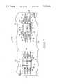
- FIG. 2is a diagrammatic top view of a portion of the FIG. 1 multichip module showing one chip stack as would be taken through line 2--2 in FIG. 1.
- FIG. 3is a diagrammatic top view of the FIG. 1 multichip module.
- FIG. 4is a diagrammatic side elevational view of an alternate embodiment multichip module in accordance with the invention.
- FIG. 5is a diagrammatic side elevational view of a further alternate multichip module in accordance with the invention.
- FIG. 6is a diagrammatic side elevational view of still a further alternate multichip module in accordance with the invention.
- a multichip modulecomprises:
- first chiphaving opposed base and bonding faces, the base face being adhered to the multichip module substrate, the first chip bonding face including a central area and a plurality of bonding pads peripheral to the central area;
- the second chiphaving opposed base and bonding faces, the second chip bonding face including a central area and a plurality of peripheral bonding pads;
- first/second adhesive layerinterposed between and connecting the first chip bonding face and the second chip base face, the first/second adhesive layer having a thickness and a perimeter, the perimeter being positioned within the central area inside of the peripheral bonding pads;
- first bonding wiresbonded to and between the respective first chip bonding pads and the multichip module substrate, the respective first bonding wires having outwardly projecting loops of a defined loop height, the thickness of the adhesive layer being greater than the loop height to displace the second chip base face in a non-contacting relationship above and with respect to the first wires;
- a multichip moduleis indicated generally with reference numeral 10.
- a multichip module substrate 12which is fabricated to comprise a plurality of z-direction multichip stacks 14 and 16.
- stack 14such includes a first chip 18 having opposed base and bonding faces 20 and 22, respectively.
- Base face 20is adhered to multichip module substrate 12 by means of an adhesive, such as epoxy, thermoplastic materials, tape, tape coated with thermoplastic materials, etc.
- First chip bonding face 22includes a central area 24 and a plurality of bonding pads 26 which are peripheral to central area 24.
- Multichip stack 14also includes a second chip 28 having opposed base and bonding faces 30, 32, respectively.
- Second chip bonding face 32includes a central area 34 and a plurality of bonding pads 36 peripheral to central area 34.
- a first/second adhesive layer 38is interposed between and connects first chip bonding face 22 and second chip base face 30.
- First/second adhesive layer 38has a thickness 40 and is deposited to define an adhesive perimeter 42, with perimeter 42 being positioned within central area 24 inside of peripheral bonding pads 26.
- a plurality of first loop bonding wires 44is bonded to and between respective first chip bonding pads 26 and multichip module substrate 12.
- First bonding wires 44have outwardly projecting loops 46 having a defined loop height 48 between upper bonding surface 22 and the maximum extent of the loop. Thickness 40 of adhesive 38 is greater than loop height 48 to displace second chip base face 30 in a non-contacting relationship above and with respect to first bonding wires 44.
- a plurality of second loop bonding wires 50is bonded to and between respective second chip bonding pads 36 and multichip module substrate 12.
- Example materials for adhesive 38include epoxies and tape. Most preferred is a thermoplastic tape such as is disclosed in our U.S. Pat. Nos. 5,140,404 and 5,177,032, which are hereby incorporated by reference. An example dimension for the adhesive layer thickness is 0.008 inch, while an example and typical defined loop height is 0.006 inch. An example of wire bonding equipment capable of producing such wire bonds and loops is the model 1484 XQ manufactured by Kulicke and Soffa Industries Inc. of Willow Groove, Pa.
- Adhesive 38preferably comprises an electrically insulating material. Wires 44 and 50 can be provided bare or be externally insulated between there respective connections to the chip bonding pads and multichip module substrate.
- Second multichip stackis substantially similar to first stack 14, and includes a subsequent second/third adhesive layer 52 and third chip 54.
- at least one additional adhesive layer and at least one additional chipis mounted outwardly relative to the second chip bonding face.
- Such third chipincludes a plurality of third chip bonding wires 56.
- Third chip 54includes a central area 58 and associated peripheral bonding pads 60 which connect with third loop wires 56.
- Third chip 54also includes an overlying adhesive layer 62. Such provides a level of additional protection to the top-most chip in a multichip stack.
- third chip 54can be considered as an outermost chip, with second/third adhesive layer 52 and/or second chip 28 and/or first/second adhesive 38 being considered as intervening material interposed between the first chip bonding face and the outermost chip base face.
- the multichip module stacks of FIGS. 1-3each include a plurality of chips of the same size and correspondingly having the same face surface areas.
- chips having different size surface areasare provided in a multichip module substrate. Referring specifically to FIG. 4, there illustrated is a first chip 64, second chip 66 and an intervening adhesive layer 68. As is apparent, the size and associated surface area of chip 66 is larger than that of chip 64. Alternately, chip 66 could be provided as a first or base chip adhered to multichip module substrate 12, with smaller chip 64 mounted there atop by adhesive.
- FIGS. 5 and 6illustrate further alternate aspects of the invention.
- FIG. 5represents a multichip module substrate having wires which are indirectly bonded to the substrate through intervening discrete electronic components.
- FIG. 5illustrates a multichip module fragment 70 having a pair of z-direction stacks 71 and 73. Such stacks are similar to the z-direction stacks described with reference to FIGS. 1-3, such that only pertinent differences are emphasized in FIG. 5 and referred to below.
- stack 71a discrete electronic component 75, such as a resistor, transistor, etc., is mounted by adhesive on multichip module substrate 12.
- a single first loop bonding wire 44abonds to discrete component 75, while a second wire 44b bonds from discrete component 75 to bulk multichip module substrate 12.
- Alternate wires interconnecting chips 28 and 18 with one another or substrate 12would also typically be provided, but are not shown for clarity.
- the z-direction stack 73is similar in construction to z-direction stack 71, and illustrates a pair of discrete electronic components 76 and 78 adhered by means of an adhesive layer 77 to an uppermost chip 85.
- a wire 79bonds between multichip module substrate 12 and discrete component 76.
- Another wire 80bonds between discrete component 76 and discrete component 78.
- Another wire 83is shown bonding from another bonding pad on chip 28 to multichip module substrate 12.
- FIG. 6illustrates another alternate multichip module 88. Such also includes a pair of z-direction stacks 87 and 89. A first wire 91 interconnects and bonds between bonding pads of the first chips of each stack 87 and 89, respectively. Further, a second wire 93 bonds with and extends between bonding pads on the outermost chips of stacks 87 and 89, respectively. Other wires are shown bonding from the respective chips to substrate 12.
Landscapes
- Engineering & Computer Science (AREA)
- Microelectronics & Electronic Packaging (AREA)
- Power Engineering (AREA)
- Computer Hardware Design (AREA)
- Physics & Mathematics (AREA)
- Condensed Matter Physics & Semiconductors (AREA)
- General Physics & Mathematics (AREA)
- Wire Bonding (AREA)
Abstract
Description
Claims (5)
Priority Applications (1)
| Application Number | Priority Date | Filing Date | Title |
|---|---|---|---|
| US08/071,580US5323060A (en) | 1993-06-02 | 1993-06-02 | Multichip module having a stacked chip arrangement |
Applications Claiming Priority (1)
| Application Number | Priority Date | Filing Date | Title |
|---|---|---|---|
| US08/071,580US5323060A (en) | 1993-06-02 | 1993-06-02 | Multichip module having a stacked chip arrangement |
Publications (1)
| Publication Number | Publication Date |
|---|---|
| US5323060Atrue US5323060A (en) | 1994-06-21 |
Family
ID=22102241
Family Applications (1)
| Application Number | Title | Priority Date | Filing Date |
|---|---|---|---|
| US08/071,580Expired - LifetimeUS5323060A (en) | 1993-06-02 | 1993-06-02 | Multichip module having a stacked chip arrangement |
Country Status (1)
| Country | Link |
|---|---|
| US (1) | US5323060A (en) |
Cited By (224)
| Publication number | Priority date | Publication date | Assignee | Title |
|---|---|---|---|---|
| US5677567A (en)* | 1996-06-17 | 1997-10-14 | Micron Technology, Inc. | Leads between chips assembly |
| US5696031A (en)* | 1996-11-20 | 1997-12-09 | Micron Technology, Inc. | Device and method for stacking wire-bonded integrated circuit dice on flip-chip bonded integrated circuit dice |
| US5721452A (en)* | 1995-08-16 | 1998-02-24 | Micron Technology, Inc. | Angularly offset stacked die multichip device and method of manufacture |
| US5760478A (en)* | 1996-08-20 | 1998-06-02 | International Business Machines Corporation | Clock skew minimization system and method for integrated circuits |
| US5777705A (en)* | 1997-05-30 | 1998-07-07 | International Business Machines Corporation | Wire bond attachment of a liquid crystal display tile to a tile carrier |
| US5801448A (en)* | 1996-05-20 | 1998-09-01 | Micron Technology, Inc. | Conductive lines on the back side of wafers and dice for semiconductor interconnects |
| US5804004A (en)* | 1992-05-11 | 1998-09-08 | Nchip, Inc. | Stacked devices for multichip modules |
| US5874781A (en)* | 1995-08-16 | 1999-02-23 | Micron Technology, Inc. | Angularly offset stacked die multichip device and method of manufacture |
| US5917242A (en)* | 1996-05-20 | 1999-06-29 | Micron Technology, Inc. | Combination of semiconductor interconnect |
| US5923090A (en)* | 1997-05-19 | 1999-07-13 | International Business Machines Corporation | Microelectronic package and fabrication thereof |
| US5952725A (en)* | 1996-02-20 | 1999-09-14 | Micron Technology, Inc. | Stacked semiconductor devices |
| US5959845A (en)* | 1997-09-18 | 1999-09-28 | International Business Machines Corporation | Universal chip carrier connector |
| US5977640A (en)* | 1998-06-26 | 1999-11-02 | International Business Machines Corporation | Highly integrated chip-on-chip packaging |
| US5994166A (en)* | 1997-03-10 | 1999-11-30 | Micron Technology, Inc. | Method of constructing stacked packages |
| US6005778A (en)* | 1995-06-15 | 1999-12-21 | Honeywell Inc. | Chip stacking and capacitor mounting arrangement including spacers |
| US6014586A (en)* | 1995-11-20 | 2000-01-11 | Pacesetter, Inc. | Vertically integrated semiconductor package for an implantable medical device |
| US6023103A (en)* | 1994-11-15 | 2000-02-08 | Formfactor, Inc. | Chip-scale carrier for semiconductor devices including mounted spring contacts |
| US6087722A (en)* | 1998-05-28 | 2000-07-11 | Samsung Electronics Co., Ltd. | Multi-chip package |
| US6147411A (en)* | 1998-03-31 | 2000-11-14 | Micron Technology, Inc. | Vertical surface mount package utilizing a back-to-back semiconductor device module |
| KR20000066816A (en)* | 1999-04-21 | 2000-11-15 | 최완균 | Method for manufacturing stacked chip package |
| US6153929A (en)* | 1998-08-21 | 2000-11-28 | Micron Technology, Inc. | Low profile multi-IC package connector |
| US6208018B1 (en) | 1997-05-29 | 2001-03-27 | Micron Technology, Inc. | Piggyback multiple dice assembly |
| US6211564B1 (en)* | 1997-12-11 | 2001-04-03 | Ricoh Company, Ltd. | Integrated circuit package having stepped terminals |
| US6215193B1 (en) | 1999-04-21 | 2001-04-10 | Advanced Semiconductor Engineering, Inc. | Multichip modules and manufacturing method therefor |
| US6225699B1 (en) | 1998-06-26 | 2001-05-01 | International Business Machines Corporation | Chip-on-chip interconnections of varied characteristics |
| US6249136B1 (en) | 1999-06-28 | 2001-06-19 | Advanced Micro Devices, Inc. | Bottom side C4 bumps for integrated circuits |
| US6252305B1 (en) | 2000-02-29 | 2001-06-26 | Advanced Semiconductor Engineering, Inc. | Multichip module having a stacked chip arrangement |
| US6261865B1 (en) | 1998-10-06 | 2001-07-17 | Micron Technology, Inc. | Multi chip semiconductor package and method of construction |
| US6262476B1 (en)* | 1998-07-27 | 2001-07-17 | Siemens Aktiengesellschaft | Composite member composed of at least two integrated circuits and method for the manufacture of a composite member composed of at least two integrated circuits |
| US6278181B1 (en) | 1999-06-28 | 2001-08-21 | Advanced Micro Devices, Inc. | Stacked multi-chip modules using C4 interconnect technology having improved thermal management |
| US20010021541A1 (en)* | 1999-06-28 | 2001-09-13 | Salman Akram | Wafer-level package and methods of fabricating |
| US6297542B1 (en) | 1998-06-25 | 2001-10-02 | Micron Technology, Inc. | Connecting a die in an integrated circuit module |
| US6313522B1 (en) | 1998-08-28 | 2001-11-06 | Micron Technology, Inc. | Semiconductor structure having stacked semiconductor devices |
| US6329221B1 (en) | 1998-03-09 | 2001-12-11 | Micron Technology, Inc. | Method of forming a stack of packaged memory die and resulting apparatus |
| US6333562B1 (en)* | 2000-07-13 | 2001-12-25 | Advanced Semiconductor Engineering, Inc. | Multichip module having stacked chip arrangement |
| US6337225B1 (en) | 2000-03-30 | 2002-01-08 | Advanced Micro Devices, Inc. | Method of making stacked die assemblies and modules |
| US6340846B1 (en) | 2000-12-06 | 2002-01-22 | Amkor Technology, Inc. | Making semiconductor packages with stacked dies and reinforced wire bonds |
| WO2002009181A1 (en)* | 2000-07-20 | 2002-01-31 | Vertical Circuits, Inc. | Vertically integrated chip on chip circuit stack |
| KR20020029251A (en)* | 2000-10-12 | 2002-04-18 | 마이클 디. 오브라이언 | Semiconductor package and its manufacturing method |
| US6387728B1 (en)* | 1999-11-09 | 2002-05-14 | Advanced Semiconductor Engineering, Inc. | Method for fabricating a stacked chip package |
| US6388313B1 (en) | 2001-01-30 | 2002-05-14 | Siliconware Precision Industries Co., Ltd. | Multi-chip module |
| US6395578B1 (en) | 1999-05-20 | 2002-05-28 | Amkor Technology, Inc. | Semiconductor package and method for fabricating the same |
| US6407456B1 (en) | 1996-02-20 | 2002-06-18 | Micron Technology, Inc. | Multi-chip device utilizing a flip chip and wire bond assembly |
| US6414391B1 (en) | 1998-06-30 | 2002-07-02 | Micron Technology, Inc. | Module assembly for stacked BGA packages with a common bus bar in the assembly |
| US6414396B1 (en) | 2000-01-24 | 2002-07-02 | Amkor Technology, Inc. | Package for stacked integrated circuits |
| KR20020056283A (en)* | 2000-12-29 | 2002-07-10 | 박종섭 | Structure of stack type muli chip semiconductor package and manufacture method the same |
| US6437449B1 (en) | 2001-04-06 | 2002-08-20 | Amkor Technology, Inc. | Making semiconductor devices having stacked dies with biased back surfaces |
| US20020125556A1 (en)* | 2001-03-09 | 2002-09-12 | Oh Kwang Seok | Stacking structure of semiconductor chips and semiconductor package using it |
| US6452278B1 (en) | 2000-06-30 | 2002-09-17 | Amkor Technology, Inc. | Low profile package for plural semiconductor dies |
| US20020131258A1 (en)* | 2001-03-14 | 2002-09-19 | Murata Manufacturing Co., Ltd. | Mounting structure for module substrates |
| US20020137252A1 (en)* | 2001-03-21 | 2002-09-26 | Larson Charles E. | Folded interposer |
| US6461956B1 (en)* | 1999-03-01 | 2002-10-08 | United Microelectronics Corp. | Method of forming package |
| WO2002082527A1 (en)* | 2001-04-05 | 2002-10-17 | Stmicroelectronics Pte Ltd | Method of forming electrical connections |
| US6472758B1 (en) | 2000-07-20 | 2002-10-29 | Amkor Technology, Inc. | Semiconductor package including stacked semiconductor dies and bond wires |
| US20020158325A1 (en)* | 1999-02-17 | 2002-10-31 | Sharp Kabushiki Kaisha | Semiconductor device and manufacturing method thereof |
| US6476502B2 (en)* | 1999-07-28 | 2002-11-05 | Mitsubishi Denki Kabushiki Kaisha | Semiconductor device and manufacturing method thereof |
| US20020167802A1 (en)* | 2001-04-24 | 2002-11-14 | Kozo Wada | Printed circuit board |
| US20020195697A1 (en)* | 2001-06-21 | 2002-12-26 | Mess Leonard E. | Stacked mass storage flash memory package |
| US6503776B2 (en) | 2001-01-05 | 2003-01-07 | Advanced Semiconductor Engineering, Inc. | Method for fabricating stacked chip package |
| US20030006494A1 (en)* | 2001-07-03 | 2003-01-09 | Lee Sang Ho | Thin profile stackable semiconductor package and method for manufacturing |
| US20030034563A1 (en)* | 2001-08-17 | 2003-02-20 | Edward Reyes | Method and apparatus for die stacking |
| US20030038356A1 (en)* | 2001-08-24 | 2003-02-27 | Derderian James M | Semiconductor devices including stacking spacers thereon, assemblies including the semiconductor devices, and methods |
| US20030038355A1 (en)* | 2001-08-24 | 2003-02-27 | Derderian James M. | Semiconductor devices and semiconductor device assemblies including a nonconfluent spacer layer |
| US6528408B2 (en) | 2001-05-21 | 2003-03-04 | Micron Technology, Inc. | Method for bumped die and wire bonded board-on-chip package |
| US20030042615A1 (en)* | 2001-08-30 | 2003-03-06 | Tongbi Jiang | Stacked microelectronic devices and methods of fabricating same |
| US6531782B1 (en) | 2001-06-19 | 2003-03-11 | Cypress Semiconductor Corp. | Method of placing die to minimize die-to-die routing complexity on a substrate |
| US6531784B1 (en) | 2000-06-02 | 2003-03-11 | Amkor Technology, Inc. | Semiconductor package with spacer strips |
| DE10157361A1 (en)* | 2001-11-23 | 2003-03-13 | Infineon Technologies Ag | Electronic component, for memory storage, comprises large semiconductor chip and small semiconductor chip, each with contact surfaces and bond wires for contacting with substrate |
| KR20030027413A (en)* | 2001-09-28 | 2003-04-07 | 삼성전자주식회사 | Multi chip package having spacer that is inserted between chips and manufacturing method thereof |
| US20030071362A1 (en)* | 2001-10-15 | 2003-04-17 | Derderian James M. | Assemblies including stacked semiconductor devices separated a distance defined by adhesive material interposed therebetween, packages including the assemblies, and methods |
| US6552416B1 (en) | 2000-09-08 | 2003-04-22 | Amkor Technology, Inc. | Multiple die lead frame package with enhanced die-to-die interconnect routing using internal lead trace wiring |
| US6552910B1 (en) | 2000-06-28 | 2003-04-22 | Micron Technology, Inc. | Stacked-die assemblies with a plurality of microelectronic devices and methods of manufacture |
| US6555917B1 (en) | 2001-10-09 | 2003-04-29 | Amkor Technology, Inc. | Semiconductor package having stacked semiconductor chips and method of making the same |
| US6560117B2 (en) | 2000-06-28 | 2003-05-06 | Micron Technology, Inc. | Packaged microelectronic die assemblies and methods of manufacture |
| US6563205B1 (en) | 1995-08-16 | 2003-05-13 | Micron Technology, Inc. | Angularly offset and recessed stacked die multichip device and method of manufacture |
| US6577013B1 (en) | 2000-09-05 | 2003-06-10 | Amkor Technology, Inc. | Chip size semiconductor packages with stacked dies |
| US6583502B2 (en) | 2001-04-17 | 2003-06-24 | Micron Technology, Inc. | Apparatus for package reduction in stacked chip and board assemblies |
| US6593662B1 (en)* | 2000-06-16 | 2003-07-15 | Siliconware Precision Industries Co., Ltd. | Stacked-die package structure |
| US20030148597A1 (en)* | 2002-01-09 | 2003-08-07 | Tan Hock Chuan | Stacked die in die BGA package |
| US6607937B1 (en)* | 2000-08-23 | 2003-08-19 | Micron Technology, Inc. | Stacked microelectronic dies and methods for stacking microelectronic dies |
| US20030160312A1 (en)* | 2002-02-28 | 2003-08-28 | Wai Yew Lo | Stacked die semiconductor device |
| EP1278243A3 (en)* | 2001-07-20 | 2003-09-03 | Optosys Technologies GmbH | Multichip Module assembled in COB structure, especially Compact Flash Card with high memory capacity and Method of Manufacturing the same |
| US6620651B2 (en) | 2001-10-23 | 2003-09-16 | National Starch And Chemical Investment Holding Corporation | Adhesive wafers for die attach application |
| US20030189256A1 (en)* | 2002-04-08 | 2003-10-09 | Corisis David J. | Bond pad rerouting element, rerouted semiconductor devices including the rerouting element, stacked chip assemblies including the rerouted semiconductor devices, and methods |
| US20030197284A1 (en)* | 2002-02-21 | 2003-10-23 | United Test & Assembly Center Limited | Semiconductor package |
| US20030199118A1 (en)* | 1999-12-20 | 2003-10-23 | Amkor Technology, Inc. | Wire bonding method for a semiconductor package |
| KR20030083306A (en)* | 2002-04-20 | 2003-10-30 | 삼성전자주식회사 | A memory card |
| US6650009B2 (en)* | 2000-07-18 | 2003-11-18 | Siliconware Precision Industries Co., Ltd. | Structure of a multi chip module having stacked chips |
| US20030214234A1 (en)* | 2002-05-20 | 2003-11-20 | Ushiodenki Kabushiki Kaisha | Discharge lamp |
| US20040007782A1 (en)* | 2002-05-15 | 2004-01-15 | Harry Hedler | Connecting circuit devices and assemblies thereof |
| US20040007771A1 (en)* | 1999-08-24 | 2004-01-15 | Amkor Technology, Inc. | Semiconductor package and method for fabricating the smae |
| US20040012079A1 (en)* | 2002-07-18 | 2004-01-22 | United Test & Assembly Center Limited Of Singapore | Multiple chip semiconductor packages |
| US6682954B1 (en) | 1996-05-29 | 2004-01-27 | Micron Technology, Inc. | Method for employing piggyback multiple die #3 |
| US6686221B1 (en) | 2002-08-30 | 2004-02-03 | Integrated Device Technology, Inc. | Method for forming packaged semiconductor device having stacked die |
| US6706557B2 (en) | 2001-09-21 | 2004-03-16 | Micron Technology, Inc. | Method of fabricating stacked die configurations utilizing redistribution bond pads |
| US20040050571A1 (en)* | 2002-09-13 | 2004-03-18 | Sang-Yeop Lee | Semiconductor chip package having an adhesive tape attached on bonding wires |
| US6717248B2 (en) | 1999-05-07 | 2004-04-06 | Amkor Technology, Inc. | Semiconductor package and method for fabricating the same |
| US20040092179A1 (en)* | 2002-11-12 | 2004-05-13 | O'rourke Maurice C. | Reset speed control for watercraft |
| US6737750B1 (en) | 2001-12-07 | 2004-05-18 | Amkor Technology, Inc. | Structures for improving heat dissipation in stacked semiconductor packages |
| US6740970B2 (en)* | 2001-05-15 | 2004-05-25 | Fujitsu Limited | Semiconductor device with stack of semiconductor chips |
| US20040102566A1 (en)* | 2002-11-25 | 2004-05-27 | Henkel Loctite Corporation | B-stageable die attach adhesives |
| US6759307B1 (en) | 2000-09-21 | 2004-07-06 | Micron Technology, Inc. | Method to prevent die attach adhesive contamination in stacked chips |
| US6759737B2 (en) | 2000-03-25 | 2004-07-06 | Amkor Technology, Inc. | Semiconductor package including stacked chips with aligned input/output pads |
| US6784019B2 (en)* | 2001-04-03 | 2004-08-31 | Siliconware Precision Industries Co., Ltd. | Intercrossedly-stacked dual-chip semiconductor package and method of fabricating the same |
| US6784023B2 (en) | 1996-05-20 | 2004-08-31 | Micron Technology, Inc. | Method of fabrication of stacked semiconductor devices |
| US20040178819A1 (en)* | 2003-03-12 | 2004-09-16 | Xilinx, Inc. | Multi-chip programmable logic device having configurable logic circuitry and configuration data storage on different dice |
| US20040212066A1 (en)* | 2003-04-23 | 2004-10-28 | Advanced Semiconductor Engineering, Inc. | Multi-chips stacked package |
| US20040212064A1 (en)* | 2003-04-23 | 2004-10-28 | Advanced Semiconductor Engineering, Inc. | Multi-chips stacked package |
| US20040212096A1 (en)* | 2003-04-23 | 2004-10-28 | Advanced Semiconductor Engineering, Inc. | Multi-chips stacked package |
| US6815251B1 (en) | 1999-02-01 | 2004-11-09 | Micron Technology, Inc. | High density modularity for IC's |
| US20040245652A1 (en)* | 2003-03-31 | 2004-12-09 | Seiko Epson Corporation | Semiconductor device, electronic device, electronic appliance, and method of manufacturing a semiconductor device |
| US20040268286A1 (en)* | 2003-06-30 | 2004-12-30 | Xilinx, Inc. | Integrated circuit with interface tile for coupling to a stacked-die second integrated circuit |
| US20050003587A1 (en)* | 2003-05-02 | 2005-01-06 | Seiko Epson Corporation | Method of manufacturing semiconductor device and method of manufacturing electronics device |
| US20050006785A1 (en)* | 2002-06-04 | 2005-01-13 | Siliconware Precision Industries Co., Ltd. | Manufacturing method for multichip module |
| US20050008832A1 (en)* | 2002-06-17 | 2005-01-13 | Santos Benedicto De Los | Interlayer dielectric and pre-applied die attach adhesive materials |
| US20050019984A1 (en)* | 2000-08-09 | 2005-01-27 | Tongbi Jiang | Multiple substrate microelectronic devices and methods of manufacture |
| US20050026415A1 (en)* | 2002-01-16 | 2005-02-03 | Micron Technology, Inc. | Fabrication of stacked microelectronic devices |
| KR100470387B1 (en)* | 2001-10-05 | 2005-02-07 | 주식회사 하이닉스반도체 | stacked chip package |
| US6867500B2 (en) | 2002-04-08 | 2005-03-15 | Micron Technology, Inc. | Multi-chip module and methods |
| US6879047B1 (en) | 2003-02-19 | 2005-04-12 | Amkor Technology, Inc. | Stacking structure for semiconductor devices using a folded over flexible substrate and method therefor |
| US6884657B1 (en) | 1995-08-16 | 2005-04-26 | Micron Technology, Inc. | Angularly offset stacked die multichip device and method of manufacture |
| US20050104183A1 (en)* | 2003-11-17 | 2005-05-19 | Renesas Technology Corp. | Multi-chip module |
| US20050112842A1 (en)* | 2003-11-24 | 2005-05-26 | Kang Jung S. | Integrating passive components on spacer in stacked dies |
| WO2005048348A1 (en)* | 2003-11-10 | 2005-05-26 | Henkel Corporation | Electronic packaging materials for use with low-k dielectric-containing semiconductor devices |
| US20050156303A1 (en)* | 2004-01-21 | 2005-07-21 | Kai-Chiang Wu | Structure of gold fingers |
| US20050156322A1 (en)* | 2001-08-31 | 2005-07-21 | Smith Lee J. | Thin semiconductor package including stacked dies |
| US6930378B1 (en) | 2003-11-10 | 2005-08-16 | Amkor Technology, Inc. | Stacked semiconductor die assembly having at least one support |
| US20050196941A1 (en)* | 2004-03-02 | 2005-09-08 | Chippac, Inc. | DBG system and method with adhesive layer severing |
| US6946323B1 (en) | 2001-11-02 | 2005-09-20 | Amkor Technology, Inc. | Semiconductor package having one or more die stacked on a prepackaged device and method therefor |
| US20050208701A1 (en)* | 2004-03-02 | 2005-09-22 | Chippac, Inc. | Semiconductor chip packaging method with individually placed film adhesive pieces |
| US20050208700A1 (en)* | 2004-03-19 | 2005-09-22 | Chippac, Inc. | Die to substrate attach using printed adhesive |
| US20050218479A1 (en)* | 2004-04-01 | 2005-10-06 | Chippac, Inc. | Spacer die structure and method for attaching |
| US20050224959A1 (en)* | 2004-04-01 | 2005-10-13 | Chippac, Inc | Die with discrete spacers and die spacing method |
| US20050258527A1 (en)* | 2004-05-24 | 2005-11-24 | Chippac, Inc. | Adhesive/spacer island structure for multiple die package |
| US20050258545A1 (en)* | 2004-05-24 | 2005-11-24 | Chippac, Inc. | Multiple die package with adhesive/spacer structure and insulated die surface |
| US20050269676A1 (en)* | 2004-05-24 | 2005-12-08 | Chippac, Inc | Adhesive/spacer island structure for stacking over wire bonded die |
| US6982485B1 (en)* | 2002-02-13 | 2006-01-03 | Amkor Technology, Inc. | Stacking structure for semiconductor chips and a semiconductor package using it |
| US20060012040A1 (en)* | 2004-05-05 | 2006-01-19 | Orient Semiconductor Electronics, Limited | Semiconductor package |
| US20060022323A1 (en)* | 2004-07-29 | 2006-02-02 | Swee Seng Eric T | Assemblies including stacked semiconductor dice having centrally located, wire bonded bond pads |
| US7023079B2 (en)* | 2001-03-01 | 2006-04-04 | Advanced Semiconductor Engineering, Inc. | Stacked semiconductor chip package |
| US20060076655A1 (en)* | 2003-05-28 | 2006-04-13 | Fernandez Elstan A | Integrated circuit package employing a flexible substrate |
| US20060097365A1 (en)* | 2004-11-09 | 2006-05-11 | Eun-Seok Song | Integrated circuit chip package having a ring-shaped silicon decoupling capacitor |
| US20060102995A1 (en)* | 2004-11-12 | 2006-05-18 | Tsai Chen J | Apparatus for stacking electrical components using insulated and interconnecting via |
| US20060102993A1 (en)* | 2004-11-12 | 2006-05-18 | Tsai Chen J | Method and apparatus for stacking electrical components using via to provide interconnection |
| SG121702A1 (en)* | 2002-01-09 | 2006-05-26 | Micron Technology Inc | Stacked die in die bga package |
| KR100600176B1 (en)* | 2000-09-19 | 2006-07-12 | 앰코 테크놀로지 코리아 주식회사 | Semiconductor Package |
| US20060151865A1 (en)* | 2004-12-10 | 2006-07-13 | Chang-Hoon Han | Semiconductor chip stack package having dummy chip |
| EP1688997A1 (en) | 2005-02-02 | 2006-08-09 | Infineon Technologies AG | Electronic component with stacked semiconductor chips and method for its manufacture |
| US20060197207A1 (en)* | 2005-02-22 | 2006-09-07 | Stats Chippac Ltd. | Integrated circuit package system with die and package combination |
| US20060197206A1 (en)* | 2005-02-22 | 2006-09-07 | Kim Dalson Y S | Stacked device package for peripheral and center device pad layout device |
| US20060202319A1 (en)* | 2004-08-19 | 2006-09-14 | Swee Seng Eric T | Assemblies and multi-chip modules including stacked semiconductor dice having centrally located, wire bonded bond pads |
| US20060238277A1 (en)* | 2001-05-09 | 2006-10-26 | Science Applications International Corporation | Phase change control devices and circuits for guiding electromagnetic waves employing phase change control devices |
| US20060246704A1 (en)* | 2005-04-27 | 2006-11-02 | Spansion Llc. | Multi-chip module and method of manufacture |
| US20060249826A1 (en)* | 2005-05-04 | 2006-11-09 | Foong Yin L | Multi-chip module and method of manufacture |
| US20060249851A1 (en)* | 2005-05-05 | 2006-11-09 | Stats Chippac Ltd. | Multiple Chip Package Module Including Die Stacked Over Encapsulated Package |
| US20060249829A1 (en)* | 2005-04-08 | 2006-11-09 | Mitsuaki Katagiri | Stacked type semiconductor device |
| KR100646468B1 (en)* | 2000-09-19 | 2006-11-14 | 앰코 테크놀로지 코리아 주식회사 | Semiconductor Package |
| US7154171B1 (en) | 2002-02-22 | 2006-12-26 | Amkor Technology, Inc. | Stacking structure for semiconductor devices using a folded over flexible substrate and method therefor |
| US20070001316A1 (en)* | 2004-07-01 | 2007-01-04 | Samsung Electronics Co., Ltd. | Semiconductor device with improved signal transmission characteristics |
| US20070018296A1 (en)* | 2004-05-24 | 2007-01-25 | Chippac, Inc | Stacked Semiconductor Package having Adhesive/Spacer Structure and Insulation |
| US20070045807A1 (en)* | 2005-09-01 | 2007-03-01 | Micron Technology, Inc. | Microelectronic devices and methods for manufacturing microelectronic devices |
| US20070052079A1 (en)* | 2005-09-07 | 2007-03-08 | Macronix International Co., Ltd. | Multi-chip stacking package structure |
| US20070085185A1 (en)* | 2005-10-19 | 2007-04-19 | Vos Chad A | Stacked integrated circuit chip assembly |
| US20070085184A1 (en)* | 2005-10-13 | 2007-04-19 | Stats Chippac Ltd. | Stacked die packaging system |
| US7211884B1 (en) | 2002-01-28 | 2007-05-01 | Pacesetter, Inc. | Implantable medical device construction using a flexible substrate |
| US20070096335A1 (en)* | 2005-10-28 | 2007-05-03 | Houng-Kyu Kwon | Chip stack structure having shielding capability and system-in-package module using the same |
| US20070120267A1 (en)* | 2005-11-28 | 2007-05-31 | Hiroshi Kuroda | Multi chip module |
| US20070170575A1 (en)* | 2006-01-26 | 2007-07-26 | Samsung Electronics Co., Ltd. | Stack chip and stack chip package having the same |
| US20070178666A1 (en)* | 2006-01-31 | 2007-08-02 | Stats Chippac Ltd. | Integrated circuit system with waferscale spacer system |
| US20070210447A1 (en)* | 2006-03-07 | 2007-09-13 | Kinsley Thomas H | Elongated fasteners for securing together electronic components and substrates, semiconductor device assemblies including such fasteners, and accompanying systems and methods |
| US20070229107A1 (en)* | 2006-04-01 | 2007-10-04 | Stats Chippac Ltd. | Stacked integrated circuit package system with connection protection |
| US20070235846A1 (en)* | 2006-04-01 | 2007-10-11 | Stats Chippac Ltd. | Integrated circuit package system with net spacer |
| US20070262431A1 (en)* | 2006-05-12 | 2007-11-15 | Hiroshi Kuroda | Semiconductor device |
| US20070284756A1 (en)* | 2006-06-12 | 2007-12-13 | Advanced Semiconductor Engineering, Inc. | Stacked chip package |
| US20070287228A1 (en)* | 2004-12-09 | 2007-12-13 | Infineon Technologies Ag | Semiconductor Package and Method of Assembling the Same |
| US20070296086A1 (en)* | 2006-06-12 | 2007-12-27 | Jong Wook Ju | Integrated circuit package system with offset stack |
| CN100361301C (en)* | 2002-06-28 | 2008-01-09 | 矽品精密工业股份有限公司 | Multi-chip semiconductor package and manufacturing method thereof |
| US20080012095A1 (en)* | 2006-07-11 | 2008-01-17 | Stats Chippac Ltd. | Integrated circuit package system including wafer level spacer |
| CN100369248C (en)* | 2004-02-13 | 2008-02-13 | 株式会社东芝 | Laminated MCP and its manufacturing method |
| US20080042245A1 (en)* | 2006-08-18 | 2008-02-21 | Stats Chippac Ltd. | Integrated circuit package system with waferscale spacer |
| USRE40112E1 (en) | 1999-05-20 | 2008-02-26 | Amkor Technology, Inc. | Semiconductor package and method for fabricating the same |
| US20080047740A1 (en)* | 2006-07-28 | 2008-02-28 | Phoenix Precision Technology Corporation | Circuit Board Assembly Having Passive Component and Stack Structure Thereof |
| US20080054433A1 (en)* | 2006-09-05 | 2008-03-06 | Samsung Electronics Co., Ltd. | Multi-chip package with spacer for blocking interchip heat transfer |
| US20080054417A1 (en)* | 2006-08-29 | 2008-03-06 | Sangdo Lee | Semiconductor die package including stacked dice and heat sink structures |
| CN100382311C (en)* | 2003-07-11 | 2008-04-16 | 旺宏电子股份有限公司 | Stack type double-chip packaging structure |
| US20080105984A1 (en)* | 2006-11-03 | 2008-05-08 | Samsung Electronics Co., Ltd. | Semiconductor chip stack package with reinforcing member for preventing package warpage connected to substrate |
| US20080113472A1 (en)* | 2006-11-09 | 2008-05-15 | Yueh Ming Tung | Film and chip packaging process using the same |
| US20080122113A1 (en)* | 2006-08-17 | 2008-05-29 | Corisis David J | Semiconductor device assemblies and systems including at least one conductive pathway extending around a side of at least one semiconductor device and methods for forming the same |
| US20080128900A1 (en)* | 2006-12-04 | 2008-06-05 | Micron Technology, Inc. | Packaged microelectronic devices and methods for manufacturing packaged microelectronic devices |
| US20080237824A1 (en)* | 2006-02-17 | 2008-10-02 | Amkor Technology, Inc. | Stacked electronic component package having single-sided film spacer |
| US20090014899A1 (en)* | 2006-01-04 | 2009-01-15 | Soo-San Park | Integrated circuit package system including stacked die |
| US7485955B2 (en) | 2004-03-22 | 2009-02-03 | Samsung Electronics Co., Ltd. | Semiconductor package having step type die and method for manufacturing the same |
| US20090091903A1 (en)* | 2006-05-24 | 2009-04-09 | Phoenix Precision Technology Corporation | Stack structure of circuit boards embedded with semiconductor chips |
| US20090121327A1 (en)* | 2007-11-08 | 2009-05-14 | Nec Electronics Corporation | Semiconductor device having spacer formed on semiconductor chip connected with wire |
| US20090161402A1 (en)* | 2007-12-20 | 2009-06-25 | Hakjune Oh | Data storage and stackable configurations |
| US20090178758A1 (en)* | 2008-01-16 | 2009-07-16 | Lingsen Precision Industries, Ltd. | Method of arranging stacked chip by photo-curing adhesive |
| US20090179318A1 (en)* | 2008-01-10 | 2009-07-16 | Abounion Technology Corporation | Multi-channel stackable semiconductor device and method for fabricating the same, and stacking substrate applied to the semiconductor device |
| US20090219772A1 (en)* | 1997-04-04 | 2009-09-03 | Leedy Glenn J | Three dimensional structure memory |
| US20090224361A1 (en)* | 2008-03-05 | 2009-09-10 | Stats Chippac, Ltd. | Semiconductor Package with Stacked Semiconductor Die each Having IPD and Method of Reducing Mutual Inductive Coupling by Providing Selectable Vertical and Lateral Separation Between IPD |
| US7633144B1 (en) | 2006-05-24 | 2009-12-15 | Amkor Technology, Inc. | Semiconductor package |
| US7656040B2 (en) | 2006-06-01 | 2010-02-02 | Phoenix Precision Technology Corporation | Stack structure of circuit board with semiconductor component embedded therein |
| US7675180B1 (en) | 2006-02-17 | 2010-03-09 | Amkor Technology, Inc. | Stacked electronic component package having film-on-wire spacer |
| US7701070B1 (en)* | 2006-12-04 | 2010-04-20 | Xilinx, Inc. | Integrated circuit and method of implementing a contact pad in an integrated circuit |
| US20100148373A1 (en)* | 2008-12-17 | 2010-06-17 | Qual.Comm Incorporated | Stacked Die Parallel Plate Capacitor |
| US20110037168A1 (en)* | 2008-07-15 | 2011-02-17 | Stats Chippac, Ltd. | Semiconductor Device and Method of Providing a Thermal Dissipation Path Through RDL and Conductive Via |
| US20110070436A1 (en)* | 2008-03-17 | 2011-03-24 | My Nguyen | Adhesive compositions for use in die attach applications |
| US20110074037A1 (en)* | 2009-09-29 | 2011-03-31 | Elpida Memory, Inc. | Semiconductor device |
| US20110133344A1 (en)* | 2009-12-07 | 2011-06-09 | Henkel Corporation | Curable resin compositions useful as underfill sealants for use with low-k dielectric-containing semiconductor devices |
| US20110304044A1 (en)* | 2010-06-15 | 2011-12-15 | Ming-Hong Lin | Stacked chip package structure and its fabrication method |
| US20120040477A1 (en)* | 2010-08-13 | 2012-02-16 | Frank Yu | Ai epoxy adjustment |
| US8296578B1 (en) | 2009-08-03 | 2012-10-23 | Xilinx, Inc. | Method and apparatus for communicating data between stacked integrated circuits |
| US8378478B2 (en) | 2010-11-24 | 2013-02-19 | Tessera, Inc. | Enhanced stacked microelectronic assemblies with central contacts and vias connected to the central contacts |
| US8384200B2 (en) | 2006-02-20 | 2013-02-26 | Micron Technology, Inc. | Semiconductor device assemblies including face-to-face semiconductor dice and systems including such assemblies |
| US8587102B2 (en) | 2002-08-08 | 2013-11-19 | Glenn J Leedy | Vertical system integration |
| US8594110B2 (en) | 2008-01-11 | 2013-11-26 | Mosaid Technologies Incorporated | Ring-of-clusters network topologies |
| US8620353B1 (en) | 2007-01-26 | 2013-12-31 | Dp Technologies, Inc. | Automatic sharing and publication of multimedia from a mobile device |
| US20140042642A1 (en)* | 2012-08-08 | 2014-02-13 | Mu-Chin Chen | Conductive line of semiconductor device and method of fabricating the same |
| US8876738B1 (en) | 2007-04-04 | 2014-11-04 | Dp Technologies, Inc. | Human activity monitoring device |
| US8902154B1 (en) | 2006-07-11 | 2014-12-02 | Dp Technologies, Inc. | Method and apparatus for utilizing motion user interface |
| US9305905B2 (en) | 2013-09-06 | 2016-04-05 | Micron Technology, Inc. | Apparatuses and related methods for staggering power-up of a stack of semiconductor dies |
| US9466545B1 (en) | 2007-02-21 | 2016-10-11 | Amkor Technology, Inc. | Semiconductor package in package |
| US9797920B2 (en) | 2008-06-24 | 2017-10-24 | DPTechnologies, Inc. | Program setting adjustments based on activity identification |
| US9859896B1 (en) | 2015-09-11 | 2018-01-02 | Xilinx, Inc. | Distributed multi-die routing in a multi-chip module |
| US9940161B1 (en) | 2007-07-27 | 2018-04-10 | Dp Technologies, Inc. | Optimizing preemptive operating system with motion sensing |
Citations (19)
| Publication number | Priority date | Publication date | Assignee | Title |
|---|---|---|---|---|
| US3851221A (en)* | 1972-11-30 | 1974-11-26 | P Beaulieu | Integrated circuit package |
| US4103318A (en)* | 1977-05-06 | 1978-07-25 | Ford Motor Company | Electronic multichip module |
| US4361261A (en)* | 1978-11-22 | 1982-11-30 | Kulicke & Soffa Industries, Inc. | Apparatus for wire bonding |
| US4444349A (en)* | 1981-05-04 | 1984-04-24 | Kulicke & Soffa Industries, Inc. | Wire bonding apparatus |
| US4567643A (en)* | 1983-10-24 | 1986-02-04 | Sintra-Alcatel | Method of replacing an electronic component connected to conducting tracks on a support substrate |
| US4586642A (en)* | 1985-05-13 | 1986-05-06 | Kulicke And Soffa Industries Inc. | Wire bond monitoring system |
| JPS62126661A (en)* | 1985-11-27 | 1987-06-08 | Nec Corp | Hybrid integrated circuit device |
| US4730232A (en)* | 1986-06-25 | 1988-03-08 | Westinghouse Electric Corp. | High density microelectronic packaging module for high speed chips |
| JPS63128736A (en)* | 1986-11-19 | 1988-06-01 | Olympus Optical Co Ltd | Semiconductor element |
| US4763188A (en)* | 1986-08-08 | 1988-08-09 | Thomas Johnson | Packaging system for multiple semiconductor devices |
| JPS63244654A (en)* | 1987-03-31 | 1988-10-12 | Toshiba Corp | Resin-encapsulated integrated circuit device |
| US4982265A (en)* | 1987-06-24 | 1991-01-01 | Hitachi, Ltd. | Semiconductor integrated circuit device and method of manufacturing the same |
| US5025306A (en)* | 1988-08-09 | 1991-06-18 | Texas Instruments Incorporated | Assembly of semiconductor chips |
| US5040052A (en)* | 1987-12-28 | 1991-08-13 | Texas Instruments Incorporated | Compact silicon module for high density integrated circuits |
| JPH0456262A (en)* | 1990-06-25 | 1992-02-24 | Matsushita Electron Corp | Semiconductor integrated circuit device |
| US5140404A (en)* | 1990-10-24 | 1992-08-18 | Micron Technology, Inc. | Semiconductor device manufactured by a method for attaching a semiconductor die to a leadframe using a thermoplastic covered carrier tape |
| US5172215A (en)* | 1990-03-06 | 1992-12-15 | Fuji Electric Co., Ltd. | Overcurrent-limiting type semiconductor device |
| US5177032A (en)* | 1990-10-24 | 1993-01-05 | Micron Technology, Inc. | Method for attaching a semiconductor die to a leadframe using a thermoplastic covered carrier tape |
| US5176311A (en)* | 1991-03-04 | 1993-01-05 | Kulicke And Soffa Investments, Inc. | High yield clampless wire bonding method |
- 1993
- 1993-06-02USUS08/071,580patent/US5323060A/ennot_activeExpired - Lifetime
Patent Citations (19)
| Publication number | Priority date | Publication date | Assignee | Title |
|---|---|---|---|---|
| US3851221A (en)* | 1972-11-30 | 1974-11-26 | P Beaulieu | Integrated circuit package |
| US4103318A (en)* | 1977-05-06 | 1978-07-25 | Ford Motor Company | Electronic multichip module |
| US4361261A (en)* | 1978-11-22 | 1982-11-30 | Kulicke & Soffa Industries, Inc. | Apparatus for wire bonding |
| US4444349A (en)* | 1981-05-04 | 1984-04-24 | Kulicke & Soffa Industries, Inc. | Wire bonding apparatus |
| US4567643A (en)* | 1983-10-24 | 1986-02-04 | Sintra-Alcatel | Method of replacing an electronic component connected to conducting tracks on a support substrate |
| US4586642A (en)* | 1985-05-13 | 1986-05-06 | Kulicke And Soffa Industries Inc. | Wire bond monitoring system |
| JPS62126661A (en)* | 1985-11-27 | 1987-06-08 | Nec Corp | Hybrid integrated circuit device |
| US4730232A (en)* | 1986-06-25 | 1988-03-08 | Westinghouse Electric Corp. | High density microelectronic packaging module for high speed chips |
| US4763188A (en)* | 1986-08-08 | 1988-08-09 | Thomas Johnson | Packaging system for multiple semiconductor devices |
| JPS63128736A (en)* | 1986-11-19 | 1988-06-01 | Olympus Optical Co Ltd | Semiconductor element |
| JPS63244654A (en)* | 1987-03-31 | 1988-10-12 | Toshiba Corp | Resin-encapsulated integrated circuit device |
| US4982265A (en)* | 1987-06-24 | 1991-01-01 | Hitachi, Ltd. | Semiconductor integrated circuit device and method of manufacturing the same |
| US5040052A (en)* | 1987-12-28 | 1991-08-13 | Texas Instruments Incorporated | Compact silicon module for high density integrated circuits |
| US5025306A (en)* | 1988-08-09 | 1991-06-18 | Texas Instruments Incorporated | Assembly of semiconductor chips |
| US5172215A (en)* | 1990-03-06 | 1992-12-15 | Fuji Electric Co., Ltd. | Overcurrent-limiting type semiconductor device |
| JPH0456262A (en)* | 1990-06-25 | 1992-02-24 | Matsushita Electron Corp | Semiconductor integrated circuit device |
| US5140404A (en)* | 1990-10-24 | 1992-08-18 | Micron Technology, Inc. | Semiconductor device manufactured by a method for attaching a semiconductor die to a leadframe using a thermoplastic covered carrier tape |
| US5177032A (en)* | 1990-10-24 | 1993-01-05 | Micron Technology, Inc. | Method for attaching a semiconductor die to a leadframe using a thermoplastic covered carrier tape |
| US5176311A (en)* | 1991-03-04 | 1993-01-05 | Kulicke And Soffa Investments, Inc. | High yield clampless wire bonding method |
Cited By (590)
| Publication number | Priority date | Publication date | Assignee | Title |
|---|---|---|---|---|
| US5804004A (en)* | 1992-05-11 | 1998-09-08 | Nchip, Inc. | Stacked devices for multichip modules |
| US6023103A (en)* | 1994-11-15 | 2000-02-08 | Formfactor, Inc. | Chip-scale carrier for semiconductor devices including mounted spring contacts |
| US6005778A (en)* | 1995-06-15 | 1999-12-21 | Honeywell Inc. | Chip stacking and capacitor mounting arrangement including spacers |
| US6563205B1 (en) | 1995-08-16 | 2003-05-13 | Micron Technology, Inc. | Angularly offset and recessed stacked die multichip device and method of manufacture |
| US6051886A (en)* | 1995-08-16 | 2000-04-18 | Micron Technology, Inc. | Angularly offset stacked die multichip device and method of manufacture |
| US5963794A (en)* | 1995-08-16 | 1999-10-05 | Micron Technology, Inc. | Angularly offset stacked die multichip device and method of manufacture |
| US5721452A (en)* | 1995-08-16 | 1998-02-24 | Micron Technology, Inc. | Angularly offset stacked die multichip device and method of manufacture |
| US6884657B1 (en) | 1995-08-16 | 2005-04-26 | Micron Technology, Inc. | Angularly offset stacked die multichip device and method of manufacture |
| US5874781A (en)* | 1995-08-16 | 1999-02-23 | Micron Technology, Inc. | Angularly offset stacked die multichip device and method of manufacture |
| US6014586A (en)* | 1995-11-20 | 2000-01-11 | Pacesetter, Inc. | Vertically integrated semiconductor package for an implantable medical device |
| US6140149A (en)* | 1996-02-20 | 2000-10-31 | Micron Technology, Inc. | Device and method for stacking wire-bonded integrated circuit dice on flip-chip bonded integrated circuit dice |
| US20070117266A1 (en)* | 1996-02-20 | 2007-05-24 | Ball Michael B | Method of fabricating a multi-die semiconductor package assembly |
| US6337227B1 (en) | 1996-02-20 | 2002-01-08 | Micron Technology, Inc. | Method of fabrication of stacked semiconductor devices |
| US5952725A (en)* | 1996-02-20 | 1999-09-14 | Micron Technology, Inc. | Stacked semiconductor devices |
| US6165815A (en)* | 1996-02-20 | 2000-12-26 | Micron Technology, Inc. | Method of fabrication of stacked semiconductor devices |
| US6407456B1 (en) | 1996-02-20 | 2002-06-18 | Micron Technology, Inc. | Multi-chip device utilizing a flip chip and wire bond assembly |
| US7166495B2 (en)* | 1996-02-20 | 2007-01-23 | Micron Technology, Inc. | Method of fabricating a multi-die semiconductor package assembly |
| US20060121645A1 (en)* | 1996-05-20 | 2006-06-08 | Ball Michael B | Method of fabrication of stacked semiconductor devices |
| US5817530A (en)* | 1996-05-20 | 1998-10-06 | Micron Technology, Inc. | Use of conductive lines on the back side of wafers and dice for semiconductor interconnects |
| US20050009236A1 (en)* | 1996-05-20 | 2005-01-13 | Ball Michael B. | Method of fabrication of stacked semiconductor devices |
| US6784023B2 (en) | 1996-05-20 | 2004-08-31 | Micron Technology, Inc. | Method of fabrication of stacked semiconductor devices |
| US7371612B2 (en) | 1996-05-20 | 2008-05-13 | Micron Technology, Inc. | Method of fabrication of stacked semiconductor devices |
| US5917242A (en)* | 1996-05-20 | 1999-06-29 | Micron Technology, Inc. | Combination of semiconductor interconnect |
| US6989285B2 (en) | 1996-05-20 | 2006-01-24 | Micron Technology, Inc. | Method of fabrication of stacked semiconductor devices |
| US6080264A (en)* | 1996-05-20 | 2000-06-27 | Micron Technology, Inc. | Combination of semiconductor interconnect |
| US5801448A (en)* | 1996-05-20 | 1998-09-01 | Micron Technology, Inc. | Conductive lines on the back side of wafers and dice for semiconductor interconnects |
| US6682954B1 (en) | 1996-05-29 | 2004-01-27 | Micron Technology, Inc. | Method for employing piggyback multiple die #3 |
| US5894165A (en)* | 1996-06-17 | 1999-04-13 | Micron Technology, Inc. | Leads between chips assembly |
| US6232148B1 (en) | 1996-06-17 | 2001-05-15 | Micron Technology, Inc. | Method and apparatus leads-between-chips |
| US5770480A (en)* | 1996-06-17 | 1998-06-23 | Micron Technology, Inc. | Method of leads between chips assembly |
| US5677567A (en)* | 1996-06-17 | 1997-10-14 | Micron Technology, Inc. | Leads between chips assembly |
| US5760478A (en)* | 1996-08-20 | 1998-06-02 | International Business Machines Corporation | Clock skew minimization system and method for integrated circuits |
| US20070063229A1 (en)* | 1996-11-20 | 2007-03-22 | Wark James M | Methods for stacking wire-bonded integrated circuit dice on flip-chip bonded integrated circuit dice |
| US7812436B2 (en) | 1996-11-20 | 2010-10-12 | Micron Technology, Inc. | Methods for stacking wire-bonded integrated circuit dice on flip-chip bonded integrated circuit dice |
| US7411286B2 (en) | 1996-11-20 | 2008-08-12 | Micron Technology, Inc. | Methods for stacking wire-bonded integrated circuit dice on flip-chip bonded integrated circuit dice |
| US7402902B2 (en) | 1996-11-20 | 2008-07-22 | Micron Technology, Inc. | Methods for stacking wire-bonded integrated circuit dice on flip-chip bonded integrated circuit dice |
| US6071754A (en)* | 1996-11-20 | 2000-06-06 | Micron Technology, Inc. | Device and method for stacking wire-bonded integrated circuit dice on flip-chip bonded integrated circuit dice |
| US20060033194A1 (en)* | 1996-11-20 | 2006-02-16 | Wark James M | Methods for stacking wire-bonded integrated circuit dice on flip-chip bonded integrated circuit dice |
| US7423338B2 (en) | 1996-11-20 | 2008-09-09 | Micron Technology, Inc. | Methods for stacking wire-bonded integrated circuit dice on flip-chip bonded integrated circuit dice |
| US6605489B2 (en) | 1996-11-20 | 2003-08-12 | Micron Technology, Inc. | Methods for stacking wire-bonded integrated circuit dice on flip-chip bonded integrated circuit dice |
| US20080315435A1 (en)* | 1996-11-20 | 2008-12-25 | Micron Technology, Inc. | Methods for stacking wire-bonded integrated circuit dice on flip-chip bonded integrated circuit dice |
| US6869826B2 (en) | 1996-11-20 | 2005-03-22 | Micron Technology, Inc. | Methods for stacking wire-bonded integrated circuit dice on flip-chip bonded integrated circuit dice |
| US20050161796A1 (en)* | 1996-11-20 | 2005-07-28 | Wark James M. | Methods for stacking wire-bonded integrated circuit dice on flip-chip bonded integrated circuit dice |
| US7423339B2 (en) | 1996-11-20 | 2008-09-09 | Mircon Technology, Inc. | Methods for stacking wire-bonded integrated circuit dice on flip-chip bonded integrated circuit dice |
| US7282792B2 (en) | 1996-11-20 | 2007-10-16 | Micron Technology, Inc. | Methods for stacking wire-bonded integrated circuit dice on flip-chip bonded integrated circuit dice |
| US7109059B2 (en) | 1996-11-20 | 2006-09-19 | Micron Technology, Inc. | Methods for stacking wire-bonded integrated circuit dice on flip-chip bonded integrated circuit dice |
| US5973403A (en)* | 1996-11-20 | 1999-10-26 | Micron Technology, Inc. | Device and method for stacking wire-bonded integrated circuit dice on flip-chip bonded integrated circuit dice |
| US6399416B1 (en) | 1996-11-20 | 2002-06-04 | Micron Technology, Inc. | Device and method for stacking wire-bonded integrated circuit dice on flip-chip bonded integrated circuit dice |
| US20040029315A1 (en)* | 1996-11-20 | 2004-02-12 | Wark James M. | Methods for stacking wire-bonded integrated circuit dice on flip-chip bonded integrated circuit dice |
| US20080311702A1 (en)* | 1996-11-20 | 2008-12-18 | Micron Technology, Inc. | Methods for stacking wire-bonded integrated circuit dice on flip-chip bonded integrated circuit dice |
| US20070063326A1 (en)* | 1996-11-20 | 2007-03-22 | Wark James M | Methods for stacking wire-bonded integrated circuit dice on flip-chip bonded integrated circuit dice |
| US7776652B2 (en) | 1996-11-20 | 2010-08-17 | Micron Technology, Inc. | Methods for stacking wire-bonded integrated circuit dice on flip-chip bonded integrated circuit dice |
| US20070063328A1 (en)* | 1996-11-20 | 2007-03-22 | Wark James M | Methods for stacking wire-bonded integrated circuit dice on flip-chip bonded integrated circuit dice |
| US20070063327A1 (en)* | 1996-11-20 | 2007-03-22 | Wark James M | Methods for stacking wire-bonded integrated circuit dice on flip-chip bonded integrated circuit dice |
| US5696031A (en)* | 1996-11-20 | 1997-12-09 | Micron Technology, Inc. | Device and method for stacking wire-bonded integrated circuit dice on flip-chip bonded integrated circuit dice |
| US6979895B2 (en) | 1997-03-10 | 2005-12-27 | Micron Technology, Inc. | Semiconductor assembly of stacked substrates and multiple semiconductor dice |
| US6404044B2 (en) | 1997-03-10 | 2002-06-11 | Micron Technology, Inc. | Semiconductor package with stacked substrates and multiple semiconductor dice |
| US6051878A (en)* | 1997-03-10 | 2000-04-18 | Micron Technology, Inc. | Method of constructing stacked packages |
| US6222265B1 (en) | 1997-03-10 | 2001-04-24 | Micron Technology, Inc. | Method of constructing stacked packages |
| US20040053442A1 (en)* | 1997-03-10 | 2004-03-18 | Salman Akram | Semiconductor package with stacked substrates and multiple semiconductor dice |
| US6583503B2 (en) | 1997-03-10 | 2003-06-24 | Micron Technology, Inc. | Semiconductor package with stacked substrates and multiple semiconductor dice |
| US5994166A (en)* | 1997-03-10 | 1999-11-30 | Micron Technology, Inc. | Method of constructing stacked packages |
| US8410617B2 (en) | 1997-04-04 | 2013-04-02 | Elm Technology | Three dimensional structure memory |
| US8933570B2 (en)* | 1997-04-04 | 2015-01-13 | Elm Technology Corp. | Three dimensional structure memory |
| US8318538B2 (en) | 1997-04-04 | 2012-11-27 | Elm Technology Corp. | Three dimensional structure memory |
| US8629542B2 (en) | 1997-04-04 | 2014-01-14 | Glenn J. Leedy | Three dimensional structure memory |
| US8928119B2 (en) | 1997-04-04 | 2015-01-06 | Glenn J. Leedy | Three dimensional structure memory |
| US9401183B2 (en) | 1997-04-04 | 2016-07-26 | Glenn J. Leedy | Stacked integrated memory device |
| US8907499B2 (en) | 1997-04-04 | 2014-12-09 | Glenn J Leedy | Three dimensional structure memory |
| US8841778B2 (en) | 1997-04-04 | 2014-09-23 | Glenn J Leedy | Three dimensional memory structure |
| US20090219772A1 (en)* | 1997-04-04 | 2009-09-03 | Leedy Glenn J | Three dimensional structure memory |
| US8791581B2 (en) | 1997-04-04 | 2014-07-29 | Glenn J Leedy | Three dimensional structure memory |
| US8796862B2 (en) | 1997-04-04 | 2014-08-05 | Glenn J Leedy | Three dimensional memory structure |
| US9087556B2 (en) | 1997-04-04 | 2015-07-21 | Glenn J Leedy | Three dimension structure memory |
| US5923090A (en)* | 1997-05-19 | 1999-07-13 | International Business Machines Corporation | Microelectronic package and fabrication thereof |
| US6208018B1 (en) | 1997-05-29 | 2001-03-27 | Micron Technology, Inc. | Piggyback multiple dice assembly |
| US5777705A (en)* | 1997-05-30 | 1998-07-07 | International Business Machines Corporation | Wire bond attachment of a liquid crystal display tile to a tile carrier |
| US5959845A (en)* | 1997-09-18 | 1999-09-28 | International Business Machines Corporation | Universal chip carrier connector |
| US6211564B1 (en)* | 1997-12-11 | 2001-04-03 | Ricoh Company, Ltd. | Integrated circuit package having stepped terminals |
| US20050170558A1 (en)* | 1998-03-09 | 2005-08-04 | King Jerrold L. | Method of forming a stack of packaged memory dice |
| US6465275B2 (en) | 1998-03-09 | 2002-10-15 | Micron Technology, Inc. | Method of forming a stack of packaged memory die and resulting apparatus |
| US7091061B2 (en) | 1998-03-09 | 2006-08-15 | Micron Technology, Inc. | Method of forming a stack of packaged memory dice |
| US6445063B1 (en) | 1998-03-09 | 2002-09-03 | Micron Technology, Inc. | Method of forming a stack of packaged memory die and resulting apparatus |
| US6656767B1 (en) | 1998-03-09 | 2003-12-02 | Micron Technology, Inc. | Method of forming a stack of packaged memory dice |
| US20040026791A1 (en)* | 1998-03-09 | 2004-02-12 | King Jerrold L. | Apparatus for forming a stack of packaged memory dice |
| US6897553B2 (en) | 1998-03-09 | 2005-05-24 | Micron Technology, Inc. | Apparatus for forming a stack of packaged memory dice |
| US6677671B2 (en) | 1998-03-09 | 2004-01-13 | Micron Technology, Inc. | Apparatus for forming a stack of packaged memory dice |
| US6884654B2 (en) | 1998-03-09 | 2005-04-26 | Micron Technology, Inc. | Method of forming a stack of packaged memory dice |
| US6329221B1 (en) | 1998-03-09 | 2001-12-11 | Micron Technology, Inc. | Method of forming a stack of packaged memory die and resulting apparatus |
| US6873037B2 (en) | 1998-03-31 | 2005-03-29 | Micron Technology, Inc. | Vertical surface mount package utilizing a back-to-back semiconductor device module |
| US6507109B2 (en) | 1998-03-31 | 2003-01-14 | Micron Technology, Inc. | Vertical surface mount package utilizing a back-to-back semiconductor device module |
| US6380630B1 (en) | 1998-03-31 | 2002-04-30 | Micron Technology, Inc. | Vertical surface mount package utilizing a back-to-back semiconductor device module |
| US7015063B2 (en) | 1998-03-31 | 2006-03-21 | Micron Technology, Inc. | Methods of utilizing a back to back semiconductor device module |
| US7282789B2 (en) | 1998-03-31 | 2007-10-16 | Micron Technology, Inc. | Back-to-back semiconductor device assemblies |
| US20050040511A1 (en)* | 1998-03-31 | 2005-02-24 | Kinsman Larry D. | Back-to-back semiconductor device assemblies |
| US20050032274A1 (en)* | 1998-03-31 | 2005-02-10 | Kinsman Larry D. | Methods for securing vertically mountable semiconductor devices in back-to back relation |
| US6417024B2 (en) | 1998-03-31 | 2002-07-09 | Micron Technology, Inc. | Back-to-back semiconductor device module, assemblies including the same and methods |
| US6147411A (en)* | 1998-03-31 | 2000-11-14 | Micron Technology, Inc. | Vertical surface mount package utilizing a back-to-back semiconductor device module |
| US7057291B2 (en) | 1998-03-31 | 2006-06-06 | Micron Technology, Inc. | Methods for securing vertically mountable semiconductor devices in back-to back relation |
| US20030102558A1 (en)* | 1998-03-31 | 2003-06-05 | Kinsman Larry D. | Vertical surface mount package utilizing a back-to-back semiconductor device module |
| US6087722A (en)* | 1998-05-28 | 2000-07-11 | Samsung Electronics Co., Ltd. | Multi-chip package |
| US6365437B2 (en) | 1998-06-25 | 2002-04-02 | Micron Technology, Inc. | Method of connecting a die in an integrated circuit module |
| US6297542B1 (en) | 1998-06-25 | 2001-10-02 | Micron Technology, Inc. | Connecting a die in an integrated circuit module |
| US6225699B1 (en) | 1998-06-26 | 2001-05-01 | International Business Machines Corporation | Chip-on-chip interconnections of varied characteristics |
| US5977640A (en)* | 1998-06-26 | 1999-11-02 | International Business Machines Corporation | Highly integrated chip-on-chip packaging |
| US6642080B1 (en) | 1998-06-26 | 2003-11-04 | International Business Machines Corporation | Chip-on-chip interconnections of varied characterstics |
| US6294406B1 (en) | 1998-06-26 | 2001-09-25 | International Business Machines Corporation | Highly integrated chip-on-chip packaging |
| US6414391B1 (en) | 1998-06-30 | 2002-07-02 | Micron Technology, Inc. | Module assembly for stacked BGA packages with a common bus bar in the assembly |
| US7279797B2 (en) | 1998-06-30 | 2007-10-09 | Micron Technology, Inc. | Module assembly and method for stacked BGA packages |
| US6563217B2 (en) | 1998-06-30 | 2003-05-13 | Micron Technology, Inc. | Module assembly for stacked BGA packages |
| US7408255B2 (en) | 1998-06-30 | 2008-08-05 | Micron Technology, Inc. | Assembly for stacked BGA packages |
| US20030197271A1 (en)* | 1998-06-30 | 2003-10-23 | Corisis David J. | Module assembly for stacked BGA packages |
| US7400032B2 (en) | 1998-06-30 | 2008-07-15 | Micron Technology, Inc. | Module assembly for stacked BGA packages |
| US7396702B2 (en) | 1998-06-30 | 2008-07-08 | Micron Technology, Inc. | Module assembly and method for stacked BGA packages |
| US20060051953A1 (en)* | 1998-06-30 | 2006-03-09 | Corisis David J | Module assembly and method for stacked BGA packages |
| US6838768B2 (en) | 1998-06-30 | 2005-01-04 | Micron Technology Inc | Module assembly for stacked BGA packages |
| US20060049504A1 (en)* | 1998-06-30 | 2006-03-09 | Corisis David J | Module assembly and method for stacked BGA packages |
| US20060060957A1 (en)* | 1998-06-30 | 2006-03-23 | Corisis David J | Module assembly and method for stacked BGA packages |
| US6262476B1 (en)* | 1998-07-27 | 2001-07-17 | Siemens Aktiengesellschaft | Composite member composed of at least two integrated circuits and method for the manufacture of a composite member composed of at least two integrated circuits |
| US6225689B1 (en) | 1998-08-21 | 2001-05-01 | Micron Technology, Inc. | Low profile multi-IC chip package connector |
| US20080003712A1 (en)* | 1998-08-21 | 2008-01-03 | Moden Walter L | Methods of making semiconductor fuses |
| US6362519B2 (en) | 1998-08-21 | 2002-03-26 | Micron Technology, Inc. | Low profile multi-IC chip package connector |
| US6153929A (en)* | 1998-08-21 | 2000-11-28 | Micron Technology, Inc. | Low profile multi-IC package connector |
| US20060252180A1 (en)* | 1998-08-21 | 2006-11-09 | Moden Walter L | Method for a low profile multi-IC chip package connector |
| US6686655B2 (en) | 1998-08-21 | 2004-02-03 | Micron Technology, Inc. | Low profile multi-IC chip package connector |
| US6258623B1 (en) | 1998-08-21 | 2001-07-10 | Micron Technology, Inc. | Low profile multi-IC chip package connector |
| US20040168316A1 (en)* | 1998-08-21 | 2004-09-02 | Moden Walter L. | Low profile multi-IC chip package connector |
| US6773955B2 (en) | 1998-08-21 | 2004-08-10 | Micron Technology, Inc. | Low profile multi-IC chip package connector |
| US6486546B2 (en) | 1998-08-21 | 2002-11-26 | Micron Technology, Inc. | Low profile multi-IC chip package connector |
| US6475831B2 (en) | 1998-08-21 | 2002-11-05 | Micron Technology, Inc. | Methods for a low profile multi-IC chip package connector |
| US7193306B2 (en) | 1998-08-28 | 2007-03-20 | Micron Technology, Inc. | Semiconductor structure having stacked semiconductor devices |
| US6531337B1 (en) | 1998-08-28 | 2003-03-11 | Micron Technology, Inc. | Method of manufacturing a semiconductor structure having stacked semiconductor devices |
| US6531338B2 (en) | 1998-08-28 | 2003-03-11 | Micron Technology, Inc. | Method of manufacturing a semiconductor structure having stacked semiconductor devices |
| US6313522B1 (en) | 1998-08-28 | 2001-11-06 | Micron Technology, Inc. | Semiconductor structure having stacked semiconductor devices |
| US20050266610A1 (en)* | 1998-08-28 | 2005-12-01 | Salman Akram | Manufacturing methods for semiconductor structures having stacked semiconductor devices |
| US6603198B2 (en) | 1998-08-28 | 2003-08-05 | Micron Technology, Inc. | Semiconductor structure having stacked semiconductor devices |
| US6673650B2 (en) | 1998-10-06 | 2004-01-06 | Micron Technology, Inc. | Multi chip semiconductor package and method of construction |
| US6261865B1 (en) | 1998-10-06 | 2001-07-17 | Micron Technology, Inc. | Multi chip semiconductor package and method of construction |
| US6458625B2 (en) | 1998-10-06 | 2002-10-01 | Micron Technology, Inc. | Multi chip semiconductor package and method of construction |
| US7061092B2 (en) | 1999-02-01 | 2006-06-13 | Micron Technology, Inc. | High-density modularity for ICS |
| US6815251B1 (en) | 1999-02-01 | 2004-11-09 | Micron Technology, Inc. | High density modularity for IC's |
| US20050148175A1 (en)* | 1999-02-17 | 2005-07-07 | Sharp Kabushiki Kaisha | Semiconductor device and manufacturing method thereof |
| US7528011B2 (en) | 1999-02-17 | 2009-05-05 | Sharp Kabushiki Kaisha | Semiconductor device and manufacturing method thereof |
| US20020158325A1 (en)* | 1999-02-17 | 2002-10-31 | Sharp Kabushiki Kaisha | Semiconductor device and manufacturing method thereof |
| US7276437B2 (en) | 1999-02-17 | 2007-10-02 | Sharp Kabushiki Kaisha | Semiconductor device and manufacturing method thereof |
| US6461956B1 (en)* | 1999-03-01 | 2002-10-08 | United Microelectronics Corp. | Method of forming package |
| KR20000066816A (en)* | 1999-04-21 | 2000-11-15 | 최완균 | Method for manufacturing stacked chip package |
| US6215193B1 (en) | 1999-04-21 | 2001-04-10 | Advanced Semiconductor Engineering, Inc. | Multichip modules and manufacturing method therefor |
| US20040164411A1 (en)* | 1999-05-07 | 2004-08-26 | Amkor Technology, Inc. | Semiconductor package and method for fabricating the same |
| US6717248B2 (en) | 1999-05-07 | 2004-04-06 | Amkor Technology, Inc. | Semiconductor package and method for fabricating the same |
| US7190071B2 (en) | 1999-05-07 | 2007-03-13 | Amkor Technology, Inc. | Semiconductor package and method for fabricating the same |
| US20040175916A1 (en)* | 1999-05-20 | 2004-09-09 | Amkor Technology, Inc. | Stackable semiconductor package having semiconductor chip within central through hole of substrate |
| US6395578B1 (en) | 1999-05-20 | 2002-05-28 | Amkor Technology, Inc. | Semiconductor package and method for fabricating the same |
| US7061120B2 (en) | 1999-05-20 | 2006-06-13 | Amkor Technology, Inc. | Stackable semiconductor package having semiconductor chip within central through hole of substrate |
| USRE40112E1 (en) | 1999-05-20 | 2008-02-26 | Amkor Technology, Inc. | Semiconductor package and method for fabricating the same |
| US6762078B2 (en) | 1999-05-20 | 2004-07-13 | Amkor Technology, Inc. | Semiconductor package having semiconductor chip within central aperture of substrate |
| US20010021541A1 (en)* | 1999-06-28 | 2001-09-13 | Salman Akram | Wafer-level package and methods of fabricating |
| US7256069B2 (en) | 1999-06-28 | 2007-08-14 | Micron Technology, Inc. | Wafer-level package and methods of fabricating |
| US6278181B1 (en) | 1999-06-28 | 2001-08-21 | Advanced Micro Devices, Inc. | Stacked multi-chip modules using C4 interconnect technology having improved thermal management |
| US6249136B1 (en) | 1999-06-28 | 2001-06-19 | Advanced Micro Devices, Inc. | Bottom side C4 bumps for integrated circuits |
| US20030085466A1 (en)* | 1999-06-28 | 2003-05-08 | Salman Akram | Chip-scale package and carrier for use therewith |
| US6873046B2 (en) | 1999-06-28 | 2005-03-29 | Micron Technology, Inc. | Chip-scale package and carrier for use therewith |
| US6476502B2 (en)* | 1999-07-28 | 2002-11-05 | Mitsubishi Denki Kabushiki Kaisha | Semiconductor device and manufacturing method thereof |
| US6982488B2 (en) | 1999-08-24 | 2006-01-03 | Amkor Technology, Inc. | Semiconductor package and method for fabricating the same |
| US6798049B1 (en) | 1999-08-24 | 2004-09-28 | Amkor Technology Inc. | Semiconductor package and method for fabricating the same |
| US20040007771A1 (en)* | 1999-08-24 | 2004-01-15 | Amkor Technology, Inc. | Semiconductor package and method for fabricating the smae |
| US20050205979A1 (en)* | 1999-08-24 | 2005-09-22 | Shin Won S | Semiconductor package and method for fabricating the same |
| US7211900B2 (en) | 1999-08-24 | 2007-05-01 | Amkor Technology, Inc. | Thin semiconductor package including stacked dies |
| US6387728B1 (en)* | 1999-11-09 | 2002-05-14 | Advanced Semiconductor Engineering, Inc. | Method for fabricating a stacked chip package |
| US6541871B2 (en) | 1999-11-09 | 2003-04-01 | Advanced Semiconductor Engineering, Inc. | Method for fabricating a stacked chip package |
| US6642610B2 (en) | 1999-12-20 | 2003-11-04 | Amkor Technology, Inc. | Wire bonding method and semiconductor package manufactured using the same |
| US20030199118A1 (en)* | 1999-12-20 | 2003-10-23 | Amkor Technology, Inc. | Wire bonding method for a semiconductor package |
| US6803254B2 (en) | 1999-12-20 | 2004-10-12 | Amkor Technology, Inc. | Wire bonding method for a semiconductor package |
| US6414396B1 (en) | 2000-01-24 | 2002-07-02 | Amkor Technology, Inc. | Package for stacked integrated circuits |
| US6461897B2 (en) | 2000-02-29 | 2002-10-08 | Advanced Semiconductor Engineering, Inc. | Multichip module having a stacked chip arrangement |
| US6252305B1 (en) | 2000-02-29 | 2001-06-26 | Advanced Semiconductor Engineering, Inc. | Multichip module having a stacked chip arrangement |
| US6759737B2 (en) | 2000-03-25 | 2004-07-06 | Amkor Technology, Inc. | Semiconductor package including stacked chips with aligned input/output pads |
| US6337225B1 (en) | 2000-03-30 | 2002-01-08 | Advanced Micro Devices, Inc. | Method of making stacked die assemblies and modules |
| US6531784B1 (en) | 2000-06-02 | 2003-03-11 | Amkor Technology, Inc. | Semiconductor package with spacer strips |
| US6593662B1 (en)* | 2000-06-16 | 2003-07-15 | Siliconware Precision Industries Co., Ltd. | Stacked-die package structure |
| US6552910B1 (en) | 2000-06-28 | 2003-04-22 | Micron Technology, Inc. | Stacked-die assemblies with a plurality of microelectronic devices and methods of manufacture |
| US6560117B2 (en) | 2000-06-28 | 2003-05-06 | Micron Technology, Inc. | Packaged microelectronic die assemblies and methods of manufacture |
| US6452278B1 (en) | 2000-06-30 | 2002-09-17 | Amkor Technology, Inc. | Low profile package for plural semiconductor dies |
| US6333562B1 (en)* | 2000-07-13 | 2001-12-25 | Advanced Semiconductor Engineering, Inc. | Multichip module having stacked chip arrangement |
| US6650009B2 (en)* | 2000-07-18 | 2003-11-18 | Siliconware Precision Industries Co., Ltd. | Structure of a multi chip module having stacked chips |
| US6472758B1 (en) | 2000-07-20 | 2002-10-29 | Amkor Technology, Inc. | Semiconductor package including stacked semiconductor dies and bond wires |
| US6650019B2 (en) | 2000-07-20 | 2003-11-18 | Amkor Technology, Inc. | Method of making a semiconductor package including stacked semiconductor dies |
| WO2002009181A1 (en)* | 2000-07-20 | 2002-01-31 | Vertical Circuits, Inc. | Vertically integrated chip on chip circuit stack |
| US7253025B2 (en) | 2000-08-09 | 2007-08-07 | Micron Technology, Inc. | Multiple substrate microelectronic devices and methods of manufacture |
| US7298031B1 (en) | 2000-08-09 | 2007-11-20 | Micron Technology, Inc. | Multiple substrate microelectronic devices and methods of manufacture |
| US20050019984A1 (en)* | 2000-08-09 | 2005-01-27 | Tongbi Jiang | Multiple substrate microelectronic devices and methods of manufacture |
| US20040038449A1 (en)* | 2000-08-23 | 2004-02-26 | Corisis David J. | Stacked microelectronic dies and methods for stacking microelectronic dies |
| US6607937B1 (en)* | 2000-08-23 | 2003-08-19 | Micron Technology, Inc. | Stacked microelectronic dies and methods for stacking microelectronic dies |
| US8067827B2 (en) | 2000-08-23 | 2011-11-29 | Micron Technology, Inc. | Stacked microelectronic device assemblies |
| US7235871B2 (en) | 2000-08-23 | 2007-06-26 | Micron Technology, Inc. | Stacked microelectronic dies |
| US20070210435A1 (en)* | 2000-08-23 | 2007-09-13 | Micron Technology, Inc. | Stacked microelectronic dies and methods for stacking microelectronic dies |
| US8587109B2 (en) | 2000-08-23 | 2013-11-19 | Micron Technology, Inc. | Stacked microelectronic dies and methods for stacking microelectronic dies |
| US6577013B1 (en) | 2000-09-05 | 2003-06-10 | Amkor Technology, Inc. | Chip size semiconductor packages with stacked dies |
| US6552416B1 (en) | 2000-09-08 | 2003-04-22 | Amkor Technology, Inc. | Multiple die lead frame package with enhanced die-to-die interconnect routing using internal lead trace wiring |
| KR100646468B1 (en)* | 2000-09-19 | 2006-11-14 | 앰코 테크놀로지 코리아 주식회사 | Semiconductor Package |
| KR100600176B1 (en)* | 2000-09-19 | 2006-07-12 | 앰코 테크놀로지 코리아 주식회사 | Semiconductor Package |
| US7078264B2 (en) | 2000-09-21 | 2006-07-18 | Micron Technology, Inc. | Stacked semiconductor die |
| US6759307B1 (en) | 2000-09-21 | 2004-07-06 | Micron Technology, Inc. | Method to prevent die attach adhesive contamination in stacked chips |
| US20040212083A1 (en)* | 2000-09-21 | 2004-10-28 | Jicheng Yang | Method to prevent die attach adhesive contamination in stacked chips |
| US20040212082A1 (en)* | 2000-09-21 | 2004-10-28 | Jicheng Yang | Method to prevent die attach adhesive contamination in stacked chips |
| US7224070B2 (en) | 2000-09-21 | 2007-05-29 | Micron Technology, Inc. | Plurality of semiconductor die in an assembly |
| KR20020029251A (en)* | 2000-10-12 | 2002-04-18 | 마이클 디. 오브라이언 | Semiconductor package and its manufacturing method |
| US6340846B1 (en) | 2000-12-06 | 2002-01-22 | Amkor Technology, Inc. | Making semiconductor packages with stacked dies and reinforced wire bonds |
| KR20020056283A (en)* | 2000-12-29 | 2002-07-10 | 박종섭 | Structure of stack type muli chip semiconductor package and manufacture method the same |
| US6503776B2 (en) | 2001-01-05 | 2003-01-07 | Advanced Semiconductor Engineering, Inc. | Method for fabricating stacked chip package |
| US6388313B1 (en) | 2001-01-30 | 2002-05-14 | Siliconware Precision Industries Co., Ltd. | Multi-chip module |
| US7023079B2 (en)* | 2001-03-01 | 2006-04-04 | Advanced Semiconductor Engineering, Inc. | Stacked semiconductor chip package |
| US20060071315A1 (en)* | 2001-03-09 | 2006-04-06 | Oh Kwang S | Method of forming a stacked semiconductor package |
| US20020125556A1 (en)* | 2001-03-09 | 2002-09-12 | Oh Kwang Seok | Stacking structure of semiconductor chips and semiconductor package using it |
| US7485490B2 (en) | 2001-03-09 | 2009-02-03 | Amkor Technology, Inc. | Method of forming a stacked semiconductor package |
| US20110089564A1 (en)* | 2001-03-09 | 2011-04-21 | Amkor Technology, Inc. | Adhesive on wire stacked semiconductor package |
| US8143727B2 (en) | 2001-03-09 | 2012-03-27 | Amkor Technology, Inc. | Adhesive on wire stacked semiconductor package |
| US20090134507A1 (en)* | 2001-03-09 | 2009-05-28 | Amkor Technology, Inc. | Adhesive on wire stacked semiconductor package |
| US7863723B2 (en) | 2001-03-09 | 2011-01-04 | Amkor Technology, Inc. | Adhesive on wire stacked semiconductor package |
| US20020131258A1 (en)* | 2001-03-14 | 2002-09-19 | Murata Manufacturing Co., Ltd. | Mounting structure for module substrates |
| US6801440B2 (en)* | 2001-03-14 | 2004-10-05 | Murata Manufacturing Co., Ltd. | Mounting structure for module substrates |
| US6982869B2 (en) | 2001-03-21 | 2006-01-03 | Micron Technology, Inc. | Folded interposer |
| US20030062614A1 (en)* | 2001-03-21 | 2003-04-03 | Larson Charles E. | Folded interposer |
| US6884653B2 (en) | 2001-03-21 | 2005-04-26 | Micron Technology, Inc. | Folded interposer |
| US20020137252A1 (en)* | 2001-03-21 | 2002-09-26 | Larson Charles E. | Folded interposer |
| US20060242477A1 (en)* | 2001-03-21 | 2006-10-26 | Larson Charles E | Folded interposer |
| US6784019B2 (en)* | 2001-04-03 | 2004-08-31 | Siliconware Precision Industries Co., Ltd. | Intercrossedly-stacked dual-chip semiconductor package and method of fabricating the same |
| WO2002082527A1 (en)* | 2001-04-05 | 2002-10-17 | Stmicroelectronics Pte Ltd | Method of forming electrical connections |
| US6437449B1 (en) | 2001-04-06 | 2002-08-20 | Amkor Technology, Inc. | Making semiconductor devices having stacked dies with biased back surfaces |
| US7005316B2 (en) | 2001-04-17 | 2006-02-28 | Micron Technology, Inc. | Method for package reduction in stacked chip and board assemblies |
| US6787917B2 (en) | 2001-04-17 | 2004-09-07 | Micron Technology, Inc. | Apparatus for package reduction in stacked chip and board assemblies |
| US6583502B2 (en) | 2001-04-17 | 2003-06-24 | Micron Technology, Inc. | Apparatus for package reduction in stacked chip and board assemblies |
| US20020167802A1 (en)* | 2001-04-24 | 2002-11-14 | Kozo Wada | Printed circuit board |
| US20060238277A1 (en)* | 2001-05-09 | 2006-10-26 | Science Applications International Corporation | Phase change control devices and circuits for guiding electromagnetic waves employing phase change control devices |
| US6740970B2 (en)* | 2001-05-15 | 2004-05-25 | Fujitsu Limited | Semiconductor device with stack of semiconductor chips |
| US6528408B2 (en) | 2001-05-21 | 2003-03-04 | Micron Technology, Inc. | Method for bumped die and wire bonded board-on-chip package |
| US7116001B2 (en) | 2001-05-21 | 2006-10-03 | Micron Technology, Inc. | Bumped die and wire bonded board-on-chip package |
| US20040169278A1 (en)* | 2001-05-21 | 2004-09-02 | Kinsman Larry D. | Bumped die and wire bonded board-on-chip package |
| US20040169203A1 (en)* | 2001-05-21 | 2004-09-02 | Kinsman Larry D. | Bumped die and wire bonded board-on-chip package |
| US6744137B2 (en) | 2001-05-21 | 2004-06-01 | Micron Technology, Inc. | Bumped die and wire bonded board-on-chip package |
| US7115990B2 (en) | 2001-05-21 | 2006-10-03 | Micron Technology, Inc. | Bumped die and wire bonded board-on-chip package |
| US6682998B2 (en) | 2001-05-21 | 2004-01-27 | Micron Technology, Inc. | Methods for bumped die and wire bonded board-on-chip package |
| US7629686B2 (en) | 2001-05-21 | 2009-12-08 | Micron Technology, Inc. | Bumped die and wire bonded board-on-chip package |
| US20070013084A1 (en)* | 2001-05-21 | 2007-01-18 | Kinsman Larry D | Bumped die and wire bonded board-on-chip package |
| US6531782B1 (en) | 2001-06-19 | 2003-03-11 | Cypress Semiconductor Corp. | Method of placing die to minimize die-to-die routing complexity on a substrate |
| US8049342B2 (en) | 2001-06-21 | 2011-11-01 | Round Rock Research, Llc | Semiconductor device and method of fabrication thereof |
| US20050029645A1 (en)* | 2001-06-21 | 2005-02-10 | Mess Leonard E. | Stacked mass storage flash memory package |
| US20100148331A1 (en)* | 2001-06-21 | 2010-06-17 | Round Rock Research, Llc | Semiconductor devices including semiconductor dice in laterally offset stacked arrangement |
| US7704794B2 (en) | 2001-06-21 | 2010-04-27 | Micron Technology, Inc. | Method of forming a semiconductor device |
| US20090286356A1 (en)* | 2001-06-21 | 2009-11-19 | Micron Technology, Inc. | Stacked mass storage flash memory package |
| US7375419B2 (en) | 2001-06-21 | 2008-05-20 | Micron Technology, Inc. | Stacked mass storage flash memory package |
| US7999378B2 (en) | 2001-06-21 | 2011-08-16 | Round Rock Research, Llc | Semiconductor devices including semiconductor dice in laterally offset stacked arrangement |
| US20070065987A1 (en)* | 2001-06-21 | 2007-03-22 | Mess Leonard E | Stacked mass storage flash memory package |
| US20020195697A1 (en)* | 2001-06-21 | 2002-12-26 | Mess Leonard E. | Stacked mass storage flash memory package |
| US6900528B2 (en) | 2001-06-21 | 2005-05-31 | Micron Technology, Inc. | Stacked mass storage flash memory package |
| US20100078793A1 (en)* | 2001-06-21 | 2010-04-01 | Micron Technology, Inc. | Semiconductor device assemblies, electronic devices including the same and assembly methods |
| US7998792B2 (en) | 2001-06-21 | 2011-08-16 | Round Rock Research, Llc | Semiconductor device assemblies, electronic devices including the same and assembly methods |
| US7262506B2 (en) | 2001-06-21 | 2007-08-28 | Micron Technology, Inc. | Stacked mass storage flash memory package |
| US20030006494A1 (en)* | 2001-07-03 | 2003-01-09 | Lee Sang Ho | Thin profile stackable semiconductor package and method for manufacturing |
| EP1278243A3 (en)* | 2001-07-20 | 2003-09-03 | Optosys Technologies GmbH | Multichip Module assembled in COB structure, especially Compact Flash Card with high memory capacity and Method of Manufacturing the same |
| US20030102569A1 (en)* | 2001-08-17 | 2003-06-05 | Edward Reyes | Method and apparatus for die stacking |
| US20030034563A1 (en)* | 2001-08-17 | 2003-02-20 | Edward Reyes | Method and apparatus for die stacking |
| US6787901B2 (en)* | 2001-08-17 | 2004-09-07 | Qualcomm Incorporated | Stacked dies utilizing cross connection bonding wire |
| US6680219B2 (en)* | 2001-08-17 | 2004-01-20 | Qualcomm Incorporated | Method and apparatus for die stacking |
| WO2003017327A3 (en)* | 2001-08-17 | 2003-11-20 | Qualcomm Inc | A method and apparatus for die stacking |
| US20060035408A1 (en)* | 2001-08-24 | 2006-02-16 | Derderian James M | Methods for designing spacers for use in stacking semiconductor devices or semiconductor device components |
| US20030038356A1 (en)* | 2001-08-24 | 2003-02-27 | Derderian James M | Semiconductor devices including stacking spacers thereon, assemblies including the semiconductor devices, and methods |
| US20030038355A1 (en)* | 2001-08-24 | 2003-02-27 | Derderian James M. | Semiconductor devices and semiconductor device assemblies including a nonconfluent spacer layer |
| US20030038357A1 (en)* | 2001-08-24 | 2003-02-27 | Derderian James M. | Spacer for semiconductor devices, semiconductor devices and assemblies including the spacer, and methods |
| US20040200885A1 (en)* | 2001-08-24 | 2004-10-14 | Derderian James M | Methods for assembling semiconductor devices in stacked arrangements by positioning spacers therebetween |
| US8101459B2 (en) | 2001-08-24 | 2012-01-24 | Micron Technology, Inc. | Methods for assembling semiconductor devices in stacked arrangements by positioning spacers therebetween |
| US7518223B2 (en) | 2001-08-24 | 2009-04-14 | Micron Technology, Inc. | Semiconductor devices and semiconductor device assemblies including a nonconfluent spacer layer |
| US20030042615A1 (en)* | 2001-08-30 | 2003-03-06 | Tongbi Jiang | Stacked microelectronic devices and methods of fabricating same |
| US7037756B1 (en) | 2001-08-30 | 2006-05-02 | Micron Technology, Inc. | Stacked microelectronic devices and methods of fabricating same |
| US20050156322A1 (en)* | 2001-08-31 | 2005-07-21 | Smith Lee J. | Thin semiconductor package including stacked dies |
| US6847105B2 (en) | 2001-09-21 | 2005-01-25 | Micron Technology, Inc. | Bumping technology in stacked die configurations |
| US6706557B2 (en) | 2001-09-21 | 2004-03-16 | Micron Technology, Inc. | Method of fabricating stacked die configurations utilizing redistribution bond pads |
| KR20030027413A (en)* | 2001-09-28 | 2003-04-07 | 삼성전자주식회사 | Multi chip package having spacer that is inserted between chips and manufacturing method thereof |
| KR100470387B1 (en)* | 2001-10-05 | 2005-02-07 | 주식회사 하이닉스반도체 | stacked chip package |
| US6555917B1 (en) | 2001-10-09 | 2003-04-29 | Amkor Technology, Inc. | Semiconductor package having stacked semiconductor chips and method of making the same |
| US7332372B2 (en)* | 2001-10-15 | 2008-02-19 | Micron Technology, Inc. | Methods for forming assemblies and packages that include stacked semiconductor devices separated a distance defined by adhesive material interposed therebetween |
| US20040157375A1 (en)* | 2001-10-15 | 2004-08-12 | Derderian James M. | Methods for forming assemblies and packages that include stacked semiconductor devices separated a distance defined by adhesive material interposed therebetween |
| US6870269B2 (en) | 2001-10-15 | 2005-03-22 | Micron Technology, Inc. | Assemblies including stacked semiconductor devices separated a distance defined by adhesive material interposed therebetween, packages including the assemblies, and methods |
| US6569709B2 (en) | 2001-10-15 | 2003-05-27 | Micron Technology, Inc. | Assemblies including stacked semiconductor devices separated a distance defined by adhesive material interposed therebetween, packages including the assemblies, and methods |
| US6869828B2 (en) | 2001-10-15 | 2005-03-22 | Micron Technology, Inc. | Assemblies including stacked semiconductor devices separated a distance defined by adhesive material interposed therebetween, packages including the assemblies, and methods |
| US7335533B2 (en) | 2001-10-15 | 2008-02-26 | Micron Technology, Inc. | Methods for assembling semiconductor devices in superimposed relation with adhesive material defining the distance adjacent semiconductor devices are spaced apart from one another |
| US20050067684A1 (en)* | 2001-10-15 | 2005-03-31 | Derderian James M. | Methods for assembling semiconductor devices in superimposed relation with adhesive material defining the distance adjacent semiconductor devices are spaced apart from one another |
| US20030071362A1 (en)* | 2001-10-15 | 2003-04-17 | Derderian James M. | Assemblies including stacked semiconductor devices separated a distance defined by adhesive material interposed therebetween, packages including the assemblies, and methods |
| US20030176018A1 (en)* | 2001-10-15 | 2003-09-18 | Derderian James M. | Assemblies including stacked semiconductor devices separated a distance defined by adhesive material interposed therebetween, packages including the assemblies, and methods |
| US6620651B2 (en) | 2001-10-23 | 2003-09-16 | National Starch And Chemical Investment Holding Corporation | Adhesive wafers for die attach application |
| US6946323B1 (en) | 2001-11-02 | 2005-09-20 | Amkor Technology, Inc. | Semiconductor package having one or more die stacked on a prepackaged device and method therefor |
| DE10157361A1 (en)* | 2001-11-23 | 2003-03-13 | Infineon Technologies Ag | Electronic component, for memory storage, comprises large semiconductor chip and small semiconductor chip, each with contact surfaces and bond wires for contacting with substrate |
| US6737750B1 (en) | 2001-12-07 | 2004-05-18 | Amkor Technology, Inc. | Structures for improving heat dissipation in stacked semiconductor packages |
| US6919631B1 (en) | 2001-12-07 | 2005-07-19 | Amkor Technology, Inc. | Structures for improving heat dissipation in stacked semiconductor packages |
| US20060292746A1 (en)* | 2002-01-09 | 2006-12-28 | Micron Technology, Inc. | Stacked die in die BGA package |
| US7358117B2 (en) | 2002-01-09 | 2008-04-15 | Micron Technology, Inc. | Stacked die in die BGA package |
| US20030148597A1 (en)* | 2002-01-09 | 2003-08-07 | Tan Hock Chuan | Stacked die in die BGA package |
| US20030207515A1 (en)* | 2002-01-09 | 2003-11-06 | Micron Technology, Inc., Boise, Id | Stacked die in die BGA package |
| US7282392B2 (en) | 2002-01-09 | 2007-10-16 | Micron Technology, Inc. | Method of fabricating a stacked die in die BGA package |
| US20030207516A1 (en)* | 2002-01-09 | 2003-11-06 | Micron Technology, Inc. | Stacked die in die BGA package |
| US7282390B2 (en) | 2002-01-09 | 2007-10-16 | Micron Technology, Inc. | Stacked die-in-die BGA package with die having a recess |
| US20080032449A1 (en)* | 2002-01-09 | 2008-02-07 | Micron Technology, Inc. | Stacked Die in Die BGA Package |
| US7332820B2 (en) | 2002-01-09 | 2008-02-19 | Micron Technology, Inc. | Stacked die in die BGA package |
| US7332819B2 (en) | 2002-01-09 | 2008-02-19 | Micron Technology, Inc. | Stacked die in die BGA package |
| SG121702A1 (en)* | 2002-01-09 | 2006-05-26 | Micron Technology Inc | Stacked die in die bga package |
| US20060216864A1 (en)* | 2002-01-09 | 2006-09-28 | Micron Technology, Inc. | Stacked die in die BGA package |
| US7309623B2 (en) | 2002-01-09 | 2007-12-18 | Micron Technology, Inc. | Method of fabricating a stacked die in die BGA package |
| US7344969B2 (en) | 2002-01-09 | 2008-03-18 | Micron Technology, Inc. | Stacked die in die BGA package |
| US8373277B2 (en) | 2002-01-09 | 2013-02-12 | Micron Technology, Inc. | Stacked die in die BGA package |
| US7575953B2 (en) | 2002-01-09 | 2009-08-18 | Micron Technology, Inc. | Stacked die with a recess in a die BGA package |
| US7799610B2 (en)* | 2002-01-09 | 2010-09-21 | Micron Technology, Inc. | Method of fabricating a stacked die having a recess in a die BGA package |
| US20080096316A1 (en)* | 2002-01-09 | 2008-04-24 | Micron Technology, Inc. | Stacked Die in Die BGA Package |
| US20060292743A1 (en)* | 2002-01-09 | 2006-12-28 | Micron Technolgoy, Inc. | Stacked die in die BGA package |
| US20060292745A1 (en)* | 2002-01-09 | 2006-12-28 | Micron Technology, Inc. | Stacked die in die BGA package |
| US7371608B2 (en) | 2002-01-09 | 2008-05-13 | Micron Technology, Inc. | Method of fabricating a stacked die having a recess in a die BGA package |
| US20080136045A1 (en)* | 2002-01-09 | 2008-06-12 | Micron Technology, Inc. | Stacked die in die BGA package |
| US20030162325A1 (en)* | 2002-01-09 | 2003-08-28 | Micron Technology, Inc. | Stacked die in die BGA package |
| US7022418B2 (en) | 2002-01-16 | 2006-04-04 | Micron Technology, Inc. | Fabrication of stacked microelectronic devices |
| US6896760B1 (en) | 2002-01-16 | 2005-05-24 | Micron Technology, Inc. | Fabrication of stacked microelectronic devices |
| US20050026395A1 (en)* | 2002-01-16 | 2005-02-03 | Micron Technology, Inc. | Fabrication of stacked microelectronic devices |
| US20050026415A1 (en)* | 2002-01-16 | 2005-02-03 | Micron Technology, Inc. | Fabrication of stacked microelectronic devices |
| US20060159947A1 (en)* | 2002-01-16 | 2006-07-20 | Micron Technology, Inc. | Fabrication of stacked microelectronic devices |
| US20060172510A1 (en)* | 2002-01-16 | 2006-08-03 | Micron Technology, Inc. | Fabrication of stacked microelectronic devices |
| US7037751B2 (en) | 2002-01-16 | 2006-05-02 | Micron Technology, Inc. | Fabrication of stacked microelectronic devices |
| US7211884B1 (en) | 2002-01-28 | 2007-05-01 | Pacesetter, Inc. | Implantable medical device construction using a flexible substrate |
| US6982485B1 (en)* | 2002-02-13 | 2006-01-03 | Amkor Technology, Inc. | Stacking structure for semiconductor chips and a semiconductor package using it |
| US8288862B2 (en) | 2002-02-21 | 2012-10-16 | United Test & Assembly Center Limited | Multiple die stack package |
| SG121705A1 (en)* | 2002-02-21 | 2006-05-26 | United Test & Assembly Ct Ltd | Semiconductor package |
| US20030197284A1 (en)* | 2002-02-21 | 2003-10-23 | United Test & Assembly Center Limited | Semiconductor package |
| US7154171B1 (en) | 2002-02-22 | 2006-12-26 | Amkor Technology, Inc. | Stacking structure for semiconductor devices using a folded over flexible substrate and method therefor |
| US20030160312A1 (en)* | 2002-02-28 | 2003-08-28 | Wai Yew Lo | Stacked die semiconductor device |
| US6885093B2 (en) | 2002-02-28 | 2005-04-26 | Freescale Semiconductor, Inc. | Stacked die semiconductor device |
| US7211466B2 (en) | 2002-02-28 | 2007-05-01 | Freescale Semiconductor, Inc. | Stacked die semiconductor device |
| US20050127491A1 (en)* | 2002-02-28 | 2005-06-16 | Lo Wai Y. | Stacked die semiconductor device |
| US20060166404A1 (en)* | 2002-04-08 | 2006-07-27 | Corisis David J | Methods for designing bond pad rerouting elements for use in stacked semiconductor device assemblies and for assembling semiconductor devices |
| US20060261492A1 (en)* | 2002-04-08 | 2006-11-23 | Corisis David J | Multi-chip module and methods |
| US7282397B2 (en) | 2002-04-08 | 2007-10-16 | Micron Technology, Inc. | Methods for designing bond pad rerouting elements for use in stacked semiconductor device assemblies and for assembling semiconductor devices |
| US7094631B2 (en) | 2002-04-08 | 2006-08-22 | Micron Technology, Inc. | Methods for designing bond pad rerouting elements for use in stacked semiconductor device assemblies and for assembling semiconductor devices |
| US6987325B2 (en) | 2002-04-08 | 2006-01-17 | Micron Technology, Inc. | Bond pad rerouting element and stacked semiconductor device assemblies including the rerouting element |
| US8048715B2 (en) | 2002-04-08 | 2011-11-01 | Round Rock Research, Llc | Multi-chip module and methods |
| US6867500B2 (en) | 2002-04-08 | 2005-03-15 | Micron Technology, Inc. | Multi-chip module and methods |
| US7084514B2 (en) | 2002-04-08 | 2006-08-01 | Micron Technology, Inc. | Multi-chip module and methods |
| US7851922B2 (en) | 2002-04-08 | 2010-12-14 | Round Rock Research, Llc | Bond pad rerouting element, rerouted semiconductor devices including the rerouting element, and assemblies including the rerouted semiconductor devices |
| US7282805B2 (en) | 2002-04-08 | 2007-10-16 | Micron Technology, Inc. | Bond pad rerouting element and stacked semiconductor device assemblies including the rerouting element |
| US7423336B2 (en) | 2002-04-08 | 2008-09-09 | Micron Technology, Inc. | Bond pad rerouting element, rerouted semiconductor devices including the rerouting element, and assemblies including the rerouted semiconductor devices |
| US20100078792A1 (en)* | 2002-04-08 | 2010-04-01 | Micron Technology, Inc. | Bond pad rerouting element, rerouted semiconductor devices including the rerouting element, and assemblies including the rerouted semiconductor devices |
| US20050146009A1 (en)* | 2002-04-08 | 2005-07-07 | Corisis David J. | Multi-chip module and methods |
| US20100055837A1 (en)* | 2002-04-08 | 2010-03-04 | Micron Technology, Inc. | Multi-chip module and methods |
| US7944057B2 (en) | 2002-04-08 | 2011-05-17 | Round Rock Research, Llc | Bond pad rerouting element, rerouted semiconductor devices including the rerouting element, and assemblies including the rerouted semiconductor devices |
| US20040036182A1 (en)* | 2002-04-08 | 2004-02-26 | Corisis David J. | Bond pad rerouting element and stacked semiconductor device assemblies including the rerouting element |
| US20090008797A1 (en)* | 2002-04-08 | 2009-01-08 | Micron Technology, Inc. | Bond pad rerouting element, rerouted semiconductor devices including the rerouting element, and assemblies including the rerouted semiconductor devices |
| US7619313B2 (en) | 2002-04-08 | 2009-11-17 | Micron Technology, Inc. | Multi-chip module and methods |
| US20030189256A1 (en)* | 2002-04-08 | 2003-10-09 | Corisis David J. | Bond pad rerouting element, rerouted semiconductor devices including the rerouting element, stacked chip assemblies including the rerouted semiconductor devices, and methods |
| US20040142506A1 (en)* | 2002-04-08 | 2004-07-22 | Corisis David J. | Methods for designing bond pad rerouting elements for use in stacked semiconductor device assemblies and for assembling semiconductor devices |
| US20060113650A1 (en)* | 2002-04-08 | 2006-06-01 | Corisis David J | Bond pad rerouting element and stacked semiconductor device assemblies including the rerouting element |
| KR20030083306A (en)* | 2002-04-20 | 2003-10-30 | 삼성전자주식회사 | A memory card |
| US20040007782A1 (en)* | 2002-05-15 | 2004-01-15 | Harry Hedler | Connecting circuit devices and assemblies thereof |
| US6897088B2 (en) | 2002-05-15 | 2005-05-24 | Infineon Technologies Ag | Method for connecting circuit devices |
| US20030214234A1 (en)* | 2002-05-20 | 2003-11-20 | Ushiodenki Kabushiki Kaisha | Discharge lamp |
| US6919627B2 (en) | 2002-06-04 | 2005-07-19 | Siliconware Precision Industries Co., Ltd. | Multichip module |
| US20050006785A1 (en)* | 2002-06-04 | 2005-01-13 | Siliconware Precision Industries Co., Ltd. | Manufacturing method for multichip module |
| US20070278683A1 (en)* | 2002-06-17 | 2007-12-06 | Henkel Corporation | Interlayer Dielectric and Pre-Applied Die Attach Adhesive Materials |
| US7550825B2 (en) | 2002-06-17 | 2009-06-23 | Henkel Corporation | Interlayer dielectric and pre-applied die attach adhesive materials |
| US7312534B2 (en) | 2002-06-17 | 2007-12-25 | Henkel Corporation | Interlayer dielectric and pre-applied die attach adhesive materials |
| US20050008832A1 (en)* | 2002-06-17 | 2005-01-13 | Santos Benedicto De Los | Interlayer dielectric and pre-applied die attach adhesive materials |
| CN100361301C (en)* | 2002-06-28 | 2008-01-09 | 矽品精密工业股份有限公司 | Multi-chip semiconductor package and manufacturing method thereof |
| US20040012079A1 (en)* | 2002-07-18 | 2004-01-22 | United Test & Assembly Center Limited Of Singapore | Multiple chip semiconductor packages |
| SG120073A1 (en)* | 2002-07-18 | 2006-03-28 | United Test & Assembly Ct Ltd | Multiple chip semiconductor packages |
| US7023076B2 (en) | 2002-07-18 | 2006-04-04 | United Test & Assembly Center Limited | Multiple chip semiconductor packages |
| US8587102B2 (en) | 2002-08-08 | 2013-11-19 | Glenn J Leedy | Vertical system integration |
| US6686221B1 (en) | 2002-08-30 | 2004-02-03 | Integrated Device Technology, Inc. | Method for forming packaged semiconductor device having stacked die |
| US20060108138A1 (en)* | 2002-09-13 | 2006-05-25 | Sang-Yeop Lee | Semiconductor chip package having an adhesive tape attached on bonding wires |
| US20040050571A1 (en)* | 2002-09-13 | 2004-03-18 | Sang-Yeop Lee | Semiconductor chip package having an adhesive tape attached on bonding wires |
| US7005577B2 (en)* | 2002-09-13 | 2006-02-28 | Samsung Electronics Co., Ltd. | Semiconductor chip package having an adhesive tape attached on bonding wires |
| US7227086B2 (en) | 2002-09-13 | 2007-06-05 | Samsung Electronics Co., Ltd | Semiconductor chip package having an adhesive tape attached on bonding wires |
| US7410832B2 (en) | 2002-09-13 | 2008-08-12 | Samsung Electronics Co., Ltd. | Semiconductor chip package having an adhesive tape attached on bonding wires |
| US20070190693A1 (en)* | 2002-09-13 | 2007-08-16 | Sang-Yeop Lee | Semiconductor chip package having an adhesive tape attached on bonding wires |
| US20040092179A1 (en)* | 2002-11-12 | 2004-05-13 | O'rourke Maurice C. | Reset speed control for watercraft |
| US20040102566A1 (en)* | 2002-11-25 | 2004-05-27 | Henkel Loctite Corporation | B-stageable die attach adhesives |
| WO2004048491A1 (en) | 2002-11-25 | 2004-06-10 | Henkel Corporation | B-stageable die attach adhesives |
| US20080160315A1 (en)* | 2002-11-25 | 2008-07-03 | Henkel Corporation | B-stageable die attach adhesives |
| US7851254B2 (en) | 2002-11-25 | 2010-12-14 | Henkel Corporation | B-stageable die attach adhesives |
| US7176044B2 (en) | 2002-11-25 | 2007-02-13 | Henkel Corporation | B-stageable die attach adhesives |
| US6879047B1 (en) | 2003-02-19 | 2005-04-12 | Amkor Technology, Inc. | Stacking structure for semiconductor devices using a folded over flexible substrate and method therefor |
| US20040178819A1 (en)* | 2003-03-12 | 2004-09-16 | Xilinx, Inc. | Multi-chip programmable logic device having configurable logic circuitry and configuration data storage on different dice |
| US6917219B2 (en) | 2003-03-12 | 2005-07-12 | Xilinx, Inc. | Multi-chip programmable logic device having configurable logic circuitry and configuration data storage on different dice |
| US20040245652A1 (en)* | 2003-03-31 | 2004-12-09 | Seiko Epson Corporation | Semiconductor device, electronic device, electronic appliance, and method of manufacturing a semiconductor device |
| US20040212064A1 (en)* | 2003-04-23 | 2004-10-28 | Advanced Semiconductor Engineering, Inc. | Multi-chips stacked package |
| US7268418B2 (en) | 2003-04-23 | 2007-09-11 | Advanced Semiconductor Engineering, Inc. | Multi-chips stacked package |
| US7002255B2 (en)* | 2003-04-23 | 2006-02-21 | Advanced Semiconductor Engineering, Inc. | Multi-chips stacked package |
| US20040212096A1 (en)* | 2003-04-23 | 2004-10-28 | Advanced Semiconductor Engineering, Inc. | Multi-chips stacked package |
| US20040212066A1 (en)* | 2003-04-23 | 2004-10-28 | Advanced Semiconductor Engineering, Inc. | Multi-chips stacked package |
| US20050003587A1 (en)* | 2003-05-02 | 2005-01-06 | Seiko Epson Corporation | Method of manufacturing semiconductor device and method of manufacturing electronics device |
| US7226808B2 (en)* | 2003-05-02 | 2007-06-05 | Seiko Epson Corporation | Method of manufacturing semiconductor device and method of manufacturing electronics device |
| US7659620B2 (en) | 2003-05-28 | 2010-02-09 | Infineon Technologies, Ag | Integrated circuit package employing a flexible substrate |
| US20060076655A1 (en)* | 2003-05-28 | 2006-04-13 | Fernandez Elstan A | Integrated circuit package employing a flexible substrate |
| US7068072B2 (en)* | 2003-06-30 | 2006-06-27 | Xilinx, Inc. | Integrated circuit with interface tile for coupling to a stacked-die second integrated circuit |
| US20040268286A1 (en)* | 2003-06-30 | 2004-12-30 | Xilinx, Inc. | Integrated circuit with interface tile for coupling to a stacked-die second integrated circuit |
| CN100382311C (en)* | 2003-07-11 | 2008-04-16 | 旺宏电子股份有限公司 | Stack type double-chip packaging structure |
| US7859119B1 (en) | 2003-11-10 | 2010-12-28 | Amkor Technology, Inc. | Stacked flip chip die assembly |
| US7071568B1 (en) | 2003-11-10 | 2006-07-04 | Amkor Technology, Inc. | Stacked-die extension support structure and method thereof |
| US7132753B1 (en) | 2003-11-10 | 2006-11-07 | Amkor Technology, Inc. | Stacked die assembly having semiconductor die overhanging support |
| CN100472768C (en)* | 2003-11-10 | 2009-03-25 | 汉高公司 | Electronic packaging materials for use with low-k dielectric-containing semiconductor devices |
| US7459776B1 (en) | 2003-11-10 | 2008-12-02 | Amkor Technology, Inc. | Stacked die assembly having semiconductor die projecting beyond support |
| WO2005048348A1 (en)* | 2003-11-10 | 2005-05-26 | Henkel Corporation | Electronic packaging materials for use with low-k dielectric-containing semiconductor devices |
| US6930378B1 (en) | 2003-11-10 | 2005-08-16 | Amkor Technology, Inc. | Stacked semiconductor die assembly having at least one support |
| US7582510B2 (en) | 2003-11-10 | 2009-09-01 | Henkel Corporation | Electronic packaging materials for use with low-k dielectric-containing semiconductor devices |
| US20080122088A1 (en)* | 2003-11-10 | 2008-05-29 | Todd Michael G | Electronic Packaging Materials for Use with Low-K Dielectric-Containing Semiconductor Devices |
| US20050104183A1 (en)* | 2003-11-17 | 2005-05-19 | Renesas Technology Corp. | Multi-chip module |
| US7009303B2 (en)* | 2003-11-17 | 2006-03-07 | Renesas Technology Corp. | Multi-chip module |
| US20050112842A1 (en)* | 2003-11-24 | 2005-05-26 | Kang Jung S. | Integrating passive components on spacer in stacked dies |
| US6937477B2 (en)* | 2004-01-21 | 2005-08-30 | Global Advanced Packaging Technology H.K. Limited | Structure of gold fingers |
| US20050156303A1 (en)* | 2004-01-21 | 2005-07-21 | Kai-Chiang Wu | Structure of gold fingers |
| CN100369248C (en)* | 2004-02-13 | 2008-02-13 | 株式会社东芝 | Laminated MCP and its manufacturing method |
| US7306971B2 (en) | 2004-03-02 | 2007-12-11 | Chippac Inc. | Semiconductor chip packaging method with individually placed film adhesive pieces |
| US20050208701A1 (en)* | 2004-03-02 | 2005-09-22 | Chippac, Inc. | Semiconductor chip packaging method with individually placed film adhesive pieces |
| US7074695B2 (en) | 2004-03-02 | 2006-07-11 | Chippac, Inc. | DBG system and method with adhesive layer severing |
| US20050196941A1 (en)* | 2004-03-02 | 2005-09-08 | Chippac, Inc. | DBG system and method with adhesive layer severing |
| US20060189101A1 (en)* | 2004-03-02 | 2006-08-24 | Chippac, Inc | DBG system and method with adhesive layer severing |
| US7420263B2 (en) | 2004-03-02 | 2008-09-02 | Chippac, Inc. | DBG system and method with adhesive layer severing |
| US20050208700A1 (en)* | 2004-03-19 | 2005-09-22 | Chippac, Inc. | Die to substrate attach using printed adhesive |
| US7485955B2 (en) | 2004-03-22 | 2009-02-03 | Samsung Electronics Co., Ltd. | Semiconductor package having step type die and method for manufacturing the same |
| US20050218479A1 (en)* | 2004-04-01 | 2005-10-06 | Chippac, Inc. | Spacer die structure and method for attaching |
| US7678611B2 (en) | 2004-04-01 | 2010-03-16 | Chippac, Inc. | Spacer die structure and method for attaching |
| US20050224959A1 (en)* | 2004-04-01 | 2005-10-13 | Chippac, Inc | Die with discrete spacers and die spacing method |
| US20060292831A1 (en)* | 2004-04-01 | 2006-12-28 | Chippac, Inc. | Spacer Die Structure and Method for Attaching |
| US7190058B2 (en) | 2004-04-01 | 2007-03-13 | Chippac, Inc. | Spacer die structure and method for attaching |
| US7394147B2 (en) | 2004-05-05 | 2008-07-01 | Orient Semiconductor Electronics, Limited | Semiconductor package |
| US20060012040A1 (en)* | 2004-05-05 | 2006-01-19 | Orient Semiconductor Electronics, Limited | Semiconductor package |
| US20050258527A1 (en)* | 2004-05-24 | 2005-11-24 | Chippac, Inc. | Adhesive/spacer island structure for multiple die package |
| US20070015314A1 (en)* | 2004-05-24 | 2007-01-18 | Chippac, Inc | Adhesive/Spacer Island Structure for Multiple Die Package |
| US8623704B2 (en) | 2004-05-24 | 2014-01-07 | Chippac, Inc. | Adhesive/spacer island structure for multiple die package |
| US8552551B2 (en) | 2004-05-24 | 2013-10-08 | Chippac, Inc. | Adhesive/spacer island structure for stacking over wire bonded die |
| US20050258545A1 (en)* | 2004-05-24 | 2005-11-24 | Chippac, Inc. | Multiple die package with adhesive/spacer structure and insulated die surface |
| US8030134B2 (en) | 2004-05-24 | 2011-10-04 | Chippac, Inc. | Stacked semiconductor package having adhesive/spacer structure and insulation |
| US20050269676A1 (en)* | 2004-05-24 | 2005-12-08 | Chippac, Inc | Adhesive/spacer island structure for stacking over wire bonded die |
| US20070018296A1 (en)* | 2004-05-24 | 2007-01-25 | Chippac, Inc | Stacked Semiconductor Package having Adhesive/Spacer Structure and Insulation |
| US20070001316A1 (en)* | 2004-07-01 | 2007-01-04 | Samsung Electronics Co., Ltd. | Semiconductor device with improved signal transmission characteristics |
| US20060022323A1 (en)* | 2004-07-29 | 2006-02-02 | Swee Seng Eric T | Assemblies including stacked semiconductor dice having centrally located, wire bonded bond pads |
| US7276790B2 (en) | 2004-07-29 | 2007-10-02 | Micron Technology, Inc. | Methods of forming a multi-chip module having discrete spacers |
| US11101245B2 (en) | 2004-07-29 | 2021-08-24 | Micron Technology, Inc. | Multi-chip modules including stacked semiconductor dice |
| US8237290B2 (en) | 2004-07-29 | 2012-08-07 | Micron Technology, Inc. | Assemblies and multi-chip modules including stacked semiconductor dice having centrally located, wire bonded bond pads |
| US9070641B2 (en) | 2004-07-29 | 2015-06-30 | Micron Technology, Inc. | Methods for forming assemblies and multi-chip modules including stacked semiconductor dice |
| US20090121338A1 (en)* | 2004-07-29 | 2009-05-14 | Micron Technology, Inc. | Assemblies and multi chip modules including stacked semiconductor dice having centrally located, wire bonded bond pads |
| US7492039B2 (en) | 2004-08-19 | 2009-02-17 | Micron Technology, Inc. | Assemblies and multi-chip modules including stacked semiconductor dice having centrally located, wire bonded bond pads |
| US20060202319A1 (en)* | 2004-08-19 | 2006-09-14 | Swee Seng Eric T | Assemblies and multi-chip modules including stacked semiconductor dice having centrally located, wire bonded bond pads |
| US7489035B2 (en) | 2004-11-09 | 2009-02-10 | Samsung Electronics Co., Ltd. | Integrated circuit chip package having a ring-shaped silicon decoupling capacitor |
| US20060097365A1 (en)* | 2004-11-09 | 2006-05-11 | Eun-Seok Song | Integrated circuit chip package having a ring-shaped silicon decoupling capacitor |
| US7892888B2 (en) | 2004-11-12 | 2011-02-22 | Macronix International Co., Ltd. | Method and apparatus for stacking electrical components using via to provide interconnection |
| US20060102993A1 (en)* | 2004-11-12 | 2006-05-18 | Tsai Chen J | Method and apparatus for stacking electrical components using via to provide interconnection |
| US7462925B2 (en) | 2004-11-12 | 2008-12-09 | Macronix International Co., Ltd. | Method and apparatus for stacking electrical components using via to provide interconnection |
| US20060102995A1 (en)* | 2004-11-12 | 2006-05-18 | Tsai Chen J | Apparatus for stacking electrical components using insulated and interconnecting via |
| US7217995B2 (en)* | 2004-11-12 | 2007-05-15 | Macronix International Co., Ltd. | Apparatus for stacking electrical components using insulated and interconnecting via |
| US20070259482A1 (en)* | 2004-11-12 | 2007-11-08 | Macronix International Co. Ltd. | Method and apparatus for stacking electrical components using via to provide interconnection |
| US20070287228A1 (en)* | 2004-12-09 | 2007-12-13 | Infineon Technologies Ag | Semiconductor Package and Method of Assembling the Same |
| US7851261B2 (en)* | 2004-12-09 | 2010-12-14 | Infineon Technologies Ag | Semiconductor package and method of assembling the same |
| US20060151865A1 (en)* | 2004-12-10 | 2006-07-13 | Chang-Hoon Han | Semiconductor chip stack package having dummy chip |
| US20060186525A1 (en)* | 2005-02-02 | 2006-08-24 | Horst Theuss | Electronic component with stacked semiconductor chips and method for producing the same |
| EP1688997A1 (en) | 2005-02-02 | 2006-08-09 | Infineon Technologies AG | Electronic component with stacked semiconductor chips and method for its manufacture |
| US7846768B2 (en) | 2005-02-22 | 2010-12-07 | Micron Technology, Inc. | Stacked die package for peripheral and center device pad layout device |
| US20060197207A1 (en)* | 2005-02-22 | 2006-09-07 | Stats Chippac Ltd. | Integrated circuit package system with die and package combination |
| US8102040B2 (en) | 2005-02-22 | 2012-01-24 | Stats Chippac Ltd. | Integrated circuit package system with die and package combination |
| US20060246622A1 (en)* | 2005-02-22 | 2006-11-02 | Kim Dalson Y S | Stacked die package for peripheral and center device pad layout device |
| US7598606B2 (en) | 2005-02-22 | 2009-10-06 | Stats Chippac Ltd. | Integrated circuit package system with die and package combination |
| US20090309207A1 (en)* | 2005-02-22 | 2009-12-17 | Seng Guan Chow | Integrated circuit package system with die and package combination |
| US8269328B2 (en) | 2005-02-22 | 2012-09-18 | Micron Technology, Inc. | Stacked die package for peripheral and center device pad layout device |
| US7425463B2 (en) | 2005-02-22 | 2008-09-16 | Micron Technology, Inc. | Stacked die package for peripheral and center device pad layout device |
| US20110062583A1 (en)* | 2005-02-22 | 2011-03-17 | Micron Technology, Inc. | Stacked die package for peripheral and center device pad layout device |
| US7205656B2 (en) | 2005-02-22 | 2007-04-17 | Micron Technology, Inc. | Stacked device package for peripheral and center device pad layout device |
| US20060197206A1 (en)* | 2005-02-22 | 2006-09-07 | Kim Dalson Y S | Stacked device package for peripheral and center device pad layout device |
| US20080280396A1 (en)* | 2005-02-22 | 2008-11-13 | Micron Technology, Inc. | Stacked die package for peripheral and center device pad layout device |
| US20060249829A1 (en)* | 2005-04-08 | 2006-11-09 | Mitsuaki Katagiri | Stacked type semiconductor device |
| US20060246704A1 (en)* | 2005-04-27 | 2006-11-02 | Spansion Llc. | Multi-chip module and method of manufacture |
| US7163839B2 (en) | 2005-04-27 | 2007-01-16 | Spansion Llc | Multi-chip module and method of manufacture |
| US8586413B2 (en) | 2005-05-04 | 2013-11-19 | Spansion Llc | Multi-chip module having a support structure and method of manufacture |
| US20060249826A1 (en)* | 2005-05-04 | 2006-11-09 | Foong Yin L | Multi-chip module and method of manufacture |
| US7582960B2 (en)* | 2005-05-05 | 2009-09-01 | Stats Chippac Ltd. | Multiple chip package module including die stacked over encapsulated package |
| US20060249851A1 (en)* | 2005-05-05 | 2006-11-09 | Stats Chippac Ltd. | Multiple Chip Package Module Including Die Stacked Over Encapsulated Package |
| US20070045807A1 (en)* | 2005-09-01 | 2007-03-01 | Micron Technology, Inc. | Microelectronic devices and methods for manufacturing microelectronic devices |
| US20070052079A1 (en)* | 2005-09-07 | 2007-03-08 | Macronix International Co., Ltd. | Multi-chip stacking package structure |
| US20070085184A1 (en)* | 2005-10-13 | 2007-04-19 | Stats Chippac Ltd. | Stacked die packaging system |
| US7429785B2 (en) | 2005-10-19 | 2008-09-30 | Littelfuse, Inc. | Stacked integrated circuit chip assembly |
| US20070085185A1 (en)* | 2005-10-19 | 2007-04-19 | Vos Chad A | Stacked integrated circuit chip assembly |
| US7723836B2 (en) | 2005-10-28 | 2010-05-25 | Samsung Electronics Co., Ltd. | Chip stack structure having shielding capability and system-in-package module using the same |
| US20070096335A1 (en)* | 2005-10-28 | 2007-05-03 | Houng-Kyu Kwon | Chip stack structure having shielding capability and system-in-package module using the same |
| US20070120267A1 (en)* | 2005-11-28 | 2007-05-31 | Hiroshi Kuroda | Multi chip module |
| US7656039B2 (en)* | 2005-11-28 | 2010-02-02 | Renesas Technology Corp. | Multi chip module |
| US7652376B2 (en)* | 2006-01-04 | 2010-01-26 | Stats Chippac Ltd. | Integrated circuit package system including stacked die |
| US20090014899A1 (en)* | 2006-01-04 | 2009-01-15 | Soo-San Park | Integrated circuit package system including stacked die |
| US7462930B2 (en) | 2006-01-26 | 2008-12-09 | Samsung Electronics Co., Ltd. | Stack chip and stack chip package having the same |
| US7768115B2 (en) | 2006-01-26 | 2010-08-03 | Samsung Electronics Co., Ltd. | Stack chip and stack chip package having the same |
| US20090065950A1 (en)* | 2006-01-26 | 2009-03-12 | Samsung Electronics Co., Ltd. | Stack chip and stack chip package having the same |
| US20070170575A1 (en)* | 2006-01-26 | 2007-07-26 | Samsung Electronics Co., Ltd. | Stack chip and stack chip package having the same |
| US20070178666A1 (en)* | 2006-01-31 | 2007-08-02 | Stats Chippac Ltd. | Integrated circuit system with waferscale spacer system |
| US20080237824A1 (en)* | 2006-02-17 | 2008-10-02 | Amkor Technology, Inc. | Stacked electronic component package having single-sided film spacer |
| US8072083B1 (en) | 2006-02-17 | 2011-12-06 | Amkor Technology, Inc. | Stacked electronic component package having film-on-wire spacer |
| US7675180B1 (en) | 2006-02-17 | 2010-03-09 | Amkor Technology, Inc. | Stacked electronic component package having film-on-wire spacer |
| US8384200B2 (en) | 2006-02-20 | 2013-02-26 | Micron Technology, Inc. | Semiconductor device assemblies including face-to-face semiconductor dice and systems including such assemblies |
| US9269695B2 (en) | 2006-02-20 | 2016-02-23 | Micron Technology, Inc. | Semiconductor device assemblies including face-to-face semiconductor dice and related methods |
| US8927332B2 (en) | 2006-02-20 | 2015-01-06 | Micron Technology, Inc. | Methods of manufacturing semiconductor device assemblies including face-to-face semiconductor dice |
| US8124456B2 (en) | 2006-03-07 | 2012-02-28 | Micron Technology, Inc. | Methods for securing semiconductor devices using elongated fasteners |
| US20070210447A1 (en)* | 2006-03-07 | 2007-09-13 | Kinsley Thomas H | Elongated fasteners for securing together electronic components and substrates, semiconductor device assemblies including such fasteners, and accompanying systems and methods |
| US7663232B2 (en) | 2006-03-07 | 2010-02-16 | Micron Technology, Inc. | Elongated fasteners for securing together electronic components and substrates, semiconductor device assemblies including such fasteners, and accompanying systems |
| US20100112754A1 (en)* | 2006-03-07 | 2010-05-06 | Micron Technology, Inc. | Methods for securing semiconductor devices using elongated fasteners |
| US7829986B2 (en) | 2006-04-01 | 2010-11-09 | Stats Chippac Ltd. | Integrated circuit package system with net spacer |
| US7443037B2 (en) | 2006-04-01 | 2008-10-28 | Stats Chippac Ltd. | Stacked integrated circuit package system with connection protection |
| US20070235846A1 (en)* | 2006-04-01 | 2007-10-11 | Stats Chippac Ltd. | Integrated circuit package system with net spacer |
| US20070229107A1 (en)* | 2006-04-01 | 2007-10-04 | Stats Chippac Ltd. | Stacked integrated circuit package system with connection protection |
| US8138611B2 (en) | 2006-05-12 | 2012-03-20 | Renesas Electronics Corporation | Semiconductor device having shifted stacked chips |
| CN101071810B (en)* | 2006-05-12 | 2010-12-22 | 瑞萨电子株式会社 | Semiconductor device |
| US20070262431A1 (en)* | 2006-05-12 | 2007-11-15 | Hiroshi Kuroda | Semiconductor device |
| US7745941B2 (en)* | 2006-05-12 | 2010-06-29 | Renesas Technology Corp. | Semiconductor device having shifted stacked chips |
| US20100219537A1 (en)* | 2006-05-12 | 2010-09-02 | Renesas Technology Corp. | Semiconductor device |
| US20090091903A1 (en)* | 2006-05-24 | 2009-04-09 | Phoenix Precision Technology Corporation | Stack structure of circuit boards embedded with semiconductor chips |
| US7633144B1 (en) | 2006-05-24 | 2009-12-15 | Amkor Technology, Inc. | Semiconductor package |
| US7706148B2 (en) | 2006-05-24 | 2010-04-27 | Phoenix Precision Technology Corporation | Stack structure of circuit boards embedded with semiconductor chips |
| US8129849B1 (en) | 2006-05-24 | 2012-03-06 | Amkor Technology, Inc. | Method of making semiconductor package with adhering portion |
| US7656040B2 (en) | 2006-06-01 | 2010-02-02 | Phoenix Precision Technology Corporation | Stack structure of circuit board with semiconductor component embedded therein |
| US20070296086A1 (en)* | 2006-06-12 | 2007-12-27 | Jong Wook Ju | Integrated circuit package system with offset stack |
| US20070284756A1 (en)* | 2006-06-12 | 2007-12-13 | Advanced Semiconductor Engineering, Inc. | Stacked chip package |
| US8659175B2 (en) | 2006-06-12 | 2014-02-25 | Stats Chippac Ltd. | Integrated circuit package system with offset stack |
| US8039365B2 (en) | 2006-07-11 | 2011-10-18 | Stats Chippac Ltd. | Integrated circuit package system including wafer level spacer |
| US20080012095A1 (en)* | 2006-07-11 | 2008-01-17 | Stats Chippac Ltd. | Integrated circuit package system including wafer level spacer |
| US8902154B1 (en) | 2006-07-11 | 2014-12-02 | Dp Technologies, Inc. | Method and apparatus for utilizing motion user interface |
| US20080047740A1 (en)* | 2006-07-28 | 2008-02-28 | Phoenix Precision Technology Corporation | Circuit Board Assembly Having Passive Component and Stack Structure Thereof |
| US20080122113A1 (en)* | 2006-08-17 | 2008-05-29 | Corisis David J | Semiconductor device assemblies and systems including at least one conductive pathway extending around a side of at least one semiconductor device and methods for forming the same |
| US7888185B2 (en)* | 2006-08-17 | 2011-02-15 | Micron Technology, Inc. | Semiconductor device assemblies and systems including at least one conductive pathway extending around a side of at least one semiconductor device |
| US8692388B2 (en) | 2006-08-18 | 2014-04-08 | Stats Chippac Ltd. | Integrated circuit package system with waferscale spacer |
| US8211749B2 (en) | 2006-08-18 | 2012-07-03 | Stats Chippac Ltd. | Integrated circuit package system with waferscale spacer |
| US20080042245A1 (en)* | 2006-08-18 | 2008-02-21 | Stats Chippac Ltd. | Integrated circuit package system with waferscale spacer |
| US20080054417A1 (en)* | 2006-08-29 | 2008-03-06 | Sangdo Lee | Semiconductor die package including stacked dice and heat sink structures |
| US7564124B2 (en) | 2006-08-29 | 2009-07-21 | Fairchild Semiconductor Corporation | Semiconductor die package including stacked dice and heat sink structures |
| CN101512756B (en)* | 2006-08-29 | 2012-10-31 | 费查尔德半导体有限公司 | Semiconductor die package including stacked dice and heat sink structures |
| WO2008027708A3 (en)* | 2006-08-29 | 2008-05-02 | Fairchild Semiconductor | Semiconductor die package including stacked dice and heat sink structures |
| US8698304B2 (en)* | 2006-09-05 | 2014-04-15 | Samsung Electronics Co., Ltd. | Multi-chip package with spacer for blocking interchip heat transfer |
| US20080054433A1 (en)* | 2006-09-05 | 2008-03-06 | Samsung Electronics Co., Ltd. | Multi-chip package with spacer for blocking interchip heat transfer |
| US20080105984A1 (en)* | 2006-11-03 | 2008-05-08 | Samsung Electronics Co., Ltd. | Semiconductor chip stack package with reinforcing member for preventing package warpage connected to substrate |
| US20080113472A1 (en)* | 2006-11-09 | 2008-05-15 | Yueh Ming Tung | Film and chip packaging process using the same |
| US20080128900A1 (en)* | 2006-12-04 | 2008-06-05 | Micron Technology, Inc. | Packaged microelectronic devices and methods for manufacturing packaged microelectronic devices |
| US8399971B2 (en) | 2006-12-04 | 2013-03-19 | Micron Technology, Inc. | Packaged microelectronic devices and methods for manufacturing packaged microelectronic devices |
| US20100237510A1 (en)* | 2006-12-04 | 2010-09-23 | Micron Technology, Inc. | Packaged microelectronic devices and methods for manufacturing packaged microelectronic devices |
| US8900923B2 (en) | 2006-12-04 | 2014-12-02 | Micron Technology, Inc. | Packaged microelectronic devices and methods for manufacturing packaged microelectronic devices |
| US7741150B2 (en) | 2006-12-04 | 2010-06-22 | Micron Technology, Inc. | Packaged microelectronic devices and methods for manufacturing packaged microelectronic devices |
| US9324676B2 (en) | 2006-12-04 | 2016-04-26 | Micron Technology, Inc. | Packaged microelectronic devices and methods for manufacturing packaged microelectronic devices |
| US7701070B1 (en)* | 2006-12-04 | 2010-04-20 | Xilinx, Inc. | Integrated circuit and method of implementing a contact pad in an integrated circuit |
| US8620353B1 (en) | 2007-01-26 | 2013-12-31 | Dp Technologies, Inc. | Automatic sharing and publication of multimedia from a mobile device |
| US9768124B2 (en) | 2007-02-21 | 2017-09-19 | Amkor Technology, Inc. | Semiconductor package in package |
| US9466545B1 (en) | 2007-02-21 | 2016-10-11 | Amkor Technology, Inc. | Semiconductor package in package |
| US8876738B1 (en) | 2007-04-04 | 2014-11-04 | Dp Technologies, Inc. | Human activity monitoring device |
| US10754683B1 (en) | 2007-07-27 | 2020-08-25 | Dp Technologies, Inc. | Optimizing preemptive operating system with motion sensing |
| US9940161B1 (en) | 2007-07-27 | 2018-04-10 | Dp Technologies, Inc. | Optimizing preemptive operating system with motion sensing |
| US7906854B2 (en)* | 2007-11-08 | 2011-03-15 | Renesas Electronics Corporation | Semiconductor device having spacer formed on semiconductor chip connected with wire |
| US20090121327A1 (en)* | 2007-11-08 | 2009-05-14 | Nec Electronics Corporation | Semiconductor device having spacer formed on semiconductor chip connected with wire |
| US9183892B2 (en) | 2007-12-20 | 2015-11-10 | Conversant Intellectual Property Management Inc. | Data storage and stackable chip configurations |
| US8399973B2 (en) | 2007-12-20 | 2013-03-19 | Mosaid Technologies Incorporated | Data storage and stackable configurations |
| US20090161402A1 (en)* | 2007-12-20 | 2009-06-25 | Hakjune Oh | Data storage and stackable configurations |
| US20090179318A1 (en)* | 2008-01-10 | 2009-07-16 | Abounion Technology Corporation | Multi-channel stackable semiconductor device and method for fabricating the same, and stacking substrate applied to the semiconductor device |
| EP2081226A1 (en) | 2008-01-10 | 2009-07-22 | Abounion Technology Corporation | Multi-channel stackable semiconductor device and method for fabricating the same, and stacking substrate applied to the semiconductor device |
| US8594110B2 (en) | 2008-01-11 | 2013-11-26 | Mosaid Technologies Incorporated | Ring-of-clusters network topologies |
| US8902910B2 (en) | 2008-01-11 | 2014-12-02 | Conversant Intellectual Property Management Inc. | Ring-of-clusters network topologies |
| US20090178758A1 (en)* | 2008-01-16 | 2009-07-16 | Lingsen Precision Industries, Ltd. | Method of arranging stacked chip by photo-curing adhesive |
| US20090224361A1 (en)* | 2008-03-05 | 2009-09-10 | Stats Chippac, Ltd. | Semiconductor Package with Stacked Semiconductor Die each Having IPD and Method of Reducing Mutual Inductive Coupling by Providing Selectable Vertical and Lateral Separation Between IPD |
| US7892858B2 (en) | 2008-03-05 | 2011-02-22 | Stats Chippac, Ltd. | Semiconductor package with stacked semiconductor die each having IPD and method of reducing mutual inductive coupling by providing selectable vertical and lateral separation between IPD |
| US8338536B2 (en) | 2008-03-17 | 2012-12-25 | Henkel Corporation | Adhesive compositions for use in die attach applications |
| US20110070436A1 (en)* | 2008-03-17 | 2011-03-24 | My Nguyen | Adhesive compositions for use in die attach applications |
| US8835574B2 (en) | 2008-03-17 | 2014-09-16 | Henkel IP Holding GmbH | Adhesive compositions for use in die attach applications |
| US12385943B2 (en) | 2008-06-24 | 2025-08-12 | Huawei Technologies Co., Ltd. | Program setting adjustments based on activity identification |
| US12306206B2 (en) | 2008-06-24 | 2025-05-20 | Huawei Technologies Co., Ltd. | Program setting adjustments based on activity identification |
| US12196775B2 (en) | 2008-06-24 | 2025-01-14 | Huawei Technologies Co., Ltd. | Program setting adjustment based on motion data |
| US11249104B2 (en) | 2008-06-24 | 2022-02-15 | Huawei Technologies Co., Ltd. | Program setting adjustments based on activity identification |
| US9797920B2 (en) | 2008-06-24 | 2017-10-24 | DPTechnologies, Inc. | Program setting adjustments based on activity identification |
| US20110037168A1 (en)* | 2008-07-15 | 2011-02-17 | Stats Chippac, Ltd. | Semiconductor Device and Method of Providing a Thermal Dissipation Path Through RDL and Conductive Via |
| US8174098B2 (en) | 2008-07-15 | 2012-05-08 | Stats Chippac, Ltd. | Semiconductor device and method of providing a thermal dissipation path through RDL and conductive via |
| US8310061B2 (en)* | 2008-12-17 | 2012-11-13 | Qualcomm Incorporated | Stacked die parallel plate capacitor |
| US20100148373A1 (en)* | 2008-12-17 | 2010-06-17 | Qual.Comm Incorporated | Stacked Die Parallel Plate Capacitor |
| US8296578B1 (en) | 2009-08-03 | 2012-10-23 | Xilinx, Inc. | Method and apparatus for communicating data between stacked integrated circuits |
| US20110074037A1 (en)* | 2009-09-29 | 2011-03-31 | Elpida Memory, Inc. | Semiconductor device |
| US8698320B2 (en) | 2009-12-07 | 2014-04-15 | Henkel IP & Holding GmbH | Curable resin compositions useful as underfill sealants for use with low-k dielectric-containing semiconductor devices |
| US20110133344A1 (en)* | 2009-12-07 | 2011-06-09 | Henkel Corporation | Curable resin compositions useful as underfill sealants for use with low-k dielectric-containing semiconductor devices |
| US20110304044A1 (en)* | 2010-06-15 | 2011-12-15 | Ming-Hong Lin | Stacked chip package structure and its fabrication method |
| US20120040477A1 (en)* | 2010-08-13 | 2012-02-16 | Frank Yu | Ai epoxy adjustment |
| US8378478B2 (en) | 2010-11-24 | 2013-02-19 | Tessera, Inc. | Enhanced stacked microelectronic assemblies with central contacts and vias connected to the central contacts |
| US9318381B2 (en) | 2012-08-08 | 2016-04-19 | United Microelectronics Corp. | Method of fabricating conductive line of a semiconductor device |
| US20140042642A1 (en)* | 2012-08-08 | 2014-02-13 | Mu-Chin Chen | Conductive line of semiconductor device and method of fabricating the same |
| US9117820B2 (en)* | 2012-08-08 | 2015-08-25 | United Microelectronics Corp. | Conductive line of semiconductor device |
| US9785171B2 (en) | 2013-09-06 | 2017-10-10 | Micron Technology, Inc. | Apparatuses and related methods for staggering power-up of a stack of semiconductor dies |
| US11092990B2 (en) | 2013-09-06 | 2021-08-17 | Micron Technology, Inc. | Apparatuses and related methods for staggering power-up of a stack of semiconductor dies |
| US10120404B2 (en) | 2013-09-06 | 2018-11-06 | Micron Technology, Inc. | Apparatuses and related methods for staggering power-up of a stack of semiconductor dies |
| US9305905B2 (en) | 2013-09-06 | 2016-04-05 | Micron Technology, Inc. | Apparatuses and related methods for staggering power-up of a stack of semiconductor dies |
| US9859896B1 (en) | 2015-09-11 | 2018-01-02 | Xilinx, Inc. | Distributed multi-die routing in a multi-chip module |
Similar Documents
| Publication | Publication Date | Title |
|---|---|---|
| US5323060A (en) | Multichip module having a stacked chip arrangement | |
| US8143727B2 (en) | Adhesive on wire stacked semiconductor package | |
| US6461897B2 (en) | Multichip module having a stacked chip arrangement | |
| US6359340B1 (en) | Multichip module having a stacked chip arrangement | |
| US7944057B2 (en) | Bond pad rerouting element, rerouted semiconductor devices including the rerouting element, and assemblies including the rerouted semiconductor devices | |
| US7161249B2 (en) | Multi-chip package (MCP) with spacer | |
| US6333562B1 (en) | Multichip module having stacked chip arrangement | |
| US6563205B1 (en) | Angularly offset and recessed stacked die multichip device and method of manufacture | |
| US7396763B2 (en) | Semiconductor package using flexible film and method of manufacturing the same | |
| US20080026506A1 (en) | Semiconductor multi-chip package and fabrication method | |
| US6448659B1 (en) | Stacked die design with supporting O-ring | |
| US6857470B2 (en) | Stacked chip package with heat transfer wires | |
| JPH02174255A (en) | Semiconductor integrated circuit | |
| US6337226B1 (en) | Semiconductor package with supported overhanging upper die | |
| US7285847B2 (en) | Chip stack package, connecting board, and method of connecting chips | |
| JP2893522B2 (en) | BGA semiconductor package and manufacturing method thereof | |
| US7224055B2 (en) | Center pad type IC chip with jumpers, method of processing the same and multi chip package | |
| US20070284756A1 (en) | Stacked chip package | |
| JPH07283274A (en) | Semiconductor device and bonding sheet | |
| KR200225040Y1 (en) | Stacked Semiconductor Packages | |
| KR20090011966A (en) | Stacked package and its manufacturing method | |
| KR20000010427A (en) | Deposition package and method for manufacturing the same | |
| JPH02125437A (en) | Semiconductor device |
Legal Events
| Date | Code | Title | Description |
|---|---|---|---|
| AS | Assignment | Owner name:MICRON SEMICONDUCTOR, INC., IDAHO Free format text:ASSIGNMENT OF ASSIGNORS INTEREST;ASSIGNORS:FOGAL, RICH;BALL, MICHAEL B.;REEL/FRAME:006577/0451 Effective date:19930526 | |
| STPP | Information on status: patent application and granting procedure in general | Free format text:APPLICATION UNDERGOING PREEXAM PROCESSING | |
| FPAY | Fee payment | Year of fee payment:4 | |
| AS | Assignment | Owner name:MICRON TECHNOLOGY, INC., IDAHO Free format text:MERGER;ASSIGNOR:MICRON SEMICONDUCTOR, INC.;REEL/FRAME:008995/0650 Effective date:19941027 | |
| FPAY | Fee payment | Year of fee payment:8 | |
| FPAY | Fee payment | Year of fee payment:12 | |
| AS | Assignment | Owner name:ROUND ROCK RESEARCH, LLC,NEW YORK Free format text:ASSIGNMENT OF ASSIGNORS INTEREST;ASSIGNOR:MICRON TECHNOLOGY, INC.;REEL/FRAME:023786/0416 Effective date:20091223 Owner name:ROUND ROCK RESEARCH, LLC, NEW YORK Free format text:ASSIGNMENT OF ASSIGNORS INTEREST;ASSIGNOR:MICRON TECHNOLOGY, INC.;REEL/FRAME:023786/0416 Effective date:20091223 |