US5320972A - Method of forming a bipolar transistor - Google Patents
Method of forming a bipolar transistorDownload PDFInfo
- Publication number
- US5320972A US5320972AUS08/001,706US170693AUS5320972AUS 5320972 AUS5320972 AUS 5320972AUS 170693 AUS170693 AUS 170693AUS 5320972 AUS5320972 AUS 5320972A
- Authority
- US
- United States
- Prior art keywords
- region
- forming
- base
- emitter
- opening
- Prior art date
- Legal status (The legal status is an assumption and is not a legal conclusion. Google has not performed a legal analysis and makes no representation as to the accuracy of the status listed.)
- Expired - Lifetime
Links
Images


Classifications
- H—ELECTRICITY
- H10—SEMICONDUCTOR DEVICES; ELECTRIC SOLID-STATE DEVICES NOT OTHERWISE PROVIDED FOR
- H10D—INORGANIC ELECTRIC SEMICONDUCTOR DEVICES
- H10D10/00—Bipolar junction transistors [BJT]
- H10D10/01—Manufacture or treatment
- H10D10/051—Manufacture or treatment of vertical BJTs
- H—ELECTRICITY
- H10—SEMICONDUCTOR DEVICES; ELECTRIC SOLID-STATE DEVICES NOT OTHERWISE PROVIDED FOR
- H10D—INORGANIC ELECTRIC SEMICONDUCTOR DEVICES
- H10D62/00—Semiconductor bodies, or regions thereof, of devices having potential barriers
- H10D62/10—Shapes, relative sizes or dispositions of the regions of the semiconductor bodies; Shapes of the semiconductor bodies
- H10D62/17—Semiconductor regions connected to electrodes not carrying current to be rectified, amplified or switched, e.g. channel regions
- H10D62/177—Base regions of bipolar transistors, e.g. BJTs or IGBTs
- H—ELECTRICITY
- H10—SEMICONDUCTOR DEVICES; ELECTRIC SOLID-STATE DEVICES NOT OTHERWISE PROVIDED FOR
- H10D—INORGANIC ELECTRIC SEMICONDUCTOR DEVICES
- H10D84/00—Integrated devices formed in or on semiconductor substrates that comprise only semiconducting layers, e.g. on Si wafers or on GaAs-on-Si wafers
- H10D84/01—Manufacture or treatment
- H10D84/0107—Integrating at least one component covered by H10D12/00 or H10D30/00 with at least one component covered by H10D8/00, H10D10/00 or H10D18/00, e.g. integrating IGFETs with BJTs
- H10D84/0109—Integrating at least one component covered by H10D12/00 or H10D30/00 with at least one component covered by H10D8/00, H10D10/00 or H10D18/00, e.g. integrating IGFETs with BJTs the at least one component covered by H10D12/00 or H10D30/00 being a MOS device
- H—ELECTRICITY
- H10—SEMICONDUCTOR DEVICES; ELECTRIC SOLID-STATE DEVICES NOT OTHERWISE PROVIDED FOR
- H10D—INORGANIC ELECTRIC SEMICONDUCTOR DEVICES
- H10D84/00—Integrated devices formed in or on semiconductor substrates that comprise only semiconducting layers, e.g. on Si wafers or on GaAs-on-Si wafers
- H10D84/01—Manufacture or treatment
- H10D84/02—Manufacture or treatment characterised by using material-based technologies
- H10D84/03—Manufacture or treatment characterised by using material-based technologies using Group IV technology, e.g. silicon technology or silicon-carbide [SiC] technology
- H10D84/038—Manufacture or treatment characterised by using material-based technologies using Group IV technology, e.g. silicon technology or silicon-carbide [SiC] technology using silicon technology, e.g. SiGe
- H—ELECTRICITY
- H10—SEMICONDUCTOR DEVICES; ELECTRIC SOLID-STATE DEVICES NOT OTHERWISE PROVIDED FOR
- H10D—INORGANIC ELECTRIC SEMICONDUCTOR DEVICES
- H10D84/00—Integrated devices formed in or on semiconductor substrates that comprise only semiconducting layers, e.g. on Si wafers or on GaAs-on-Si wafers
- H10D84/40—Integrated devices formed in or on semiconductor substrates that comprise only semiconducting layers, e.g. on Si wafers or on GaAs-on-Si wafers characterised by the integration of at least one component covered by groups H10D12/00 or H10D30/00 with at least one component covered by groups H10D10/00 or H10D18/00, e.g. integration of IGFETs with BJTs
- H10D84/401—Combinations of FETs or IGBTs with BJTs
- Y—GENERAL TAGGING OF NEW TECHNOLOGICAL DEVELOPMENTS; GENERAL TAGGING OF CROSS-SECTIONAL TECHNOLOGIES SPANNING OVER SEVERAL SECTIONS OF THE IPC; TECHNICAL SUBJECTS COVERED BY FORMER USPC CROSS-REFERENCE ART COLLECTIONS [XRACs] AND DIGESTS
- Y10—TECHNICAL SUBJECTS COVERED BY FORMER USPC
- Y10S—TECHNICAL SUBJECTS COVERED BY FORMER USPC CROSS-REFERENCE ART COLLECTIONS [XRACs] AND DIGESTS
- Y10S148/00—Metal treatment
- Y10S148/026—Deposition thru hole in mask
- Y—GENERAL TAGGING OF NEW TECHNOLOGICAL DEVELOPMENTS; GENERAL TAGGING OF CROSS-SECTIONAL TECHNOLOGIES SPANNING OVER SEVERAL SECTIONS OF THE IPC; TECHNICAL SUBJECTS COVERED BY FORMER USPC CROSS-REFERENCE ART COLLECTIONS [XRACs] AND DIGESTS
- Y10—TECHNICAL SUBJECTS COVERED BY FORMER USPC
- Y10S—TECHNICAL SUBJECTS COVERED BY FORMER USPC CROSS-REFERENCE ART COLLECTIONS [XRACs] AND DIGESTS
- Y10S148/00—Metal treatment
- Y10S148/124—Polycrystalline emitter
- Y—GENERAL TAGGING OF NEW TECHNOLOGICAL DEVELOPMENTS; GENERAL TAGGING OF CROSS-SECTIONAL TECHNOLOGIES SPANNING OVER SEVERAL SECTIONS OF THE IPC; TECHNICAL SUBJECTS COVERED BY FORMER USPC CROSS-REFERENCE ART COLLECTIONS [XRACs] AND DIGESTS
- Y10—TECHNICAL SUBJECTS COVERED BY FORMER USPC
- Y10S—TECHNICAL SUBJECTS COVERED BY FORMER USPC CROSS-REFERENCE ART COLLECTIONS [XRACs] AND DIGESTS
- Y10S257/00—Active solid-state devices, e.g. transistors, solid-state diodes
- Y10S257/90—MOSFET type gate sidewall insulating spacer
Definitions
- This inventionrelates to a method of forming a bipolar transistor and a bipolar transistor structure.
- a conventional "double-polysilicon" structureis formed with two layers of polysilicon, using a first polysilicon layer for base electrodes and a second polysilicon layer for an emitter electrode.
- Polysiliconis a preferred emitter material compared with single crystal silicon to improve forward current gain of the transistor.
- increased doping of the basecan be used to prevent premature punchthrough when using shallow base widths required for high speed operation.
- the collector-base overlap areamay be reduced if the extrinsic base contact is opened in an area of the base polysilicon layer which extends over a field isolation layer, rather than directly over the active device area.
- the collector-base parasitic capacitanceis reduced, and reduced spacing between a self-aligned emitter and base electrodes may be achieved.
- Processesare known for fabrication of bipolar transistors having a self-aligned structure, using a first polysilicon layer for the extrinsic base contact and a second polysilicon layer for the emitter contact, for example as described in an article entitled "High Speed Polysilicon Emitter-Base Bipolar Transistor" by Hee K. Park et al., IEEE Electron Device Letters, EDL-7 No. 12 December 1986.
- Self-alignment of the base and the emitterallows for minimization of both the extrinsic base resistance and the collector-base junction capacitance.
- a typical process flowincludes the following steps: a substrate is provided in the form of semiconductor wafer having an N epitaxial (epi-)layer overlying a N+ buried layer. The latter forms a buried collector. A device well region is defined in the N epi-layer and a field oxide isolation layer is formed surrounding the device well region. Then a first (base) polysilicon layer is deposited overall, extending over the device well region. The first polysilicon layer is photoengraved (PE) and etched to open a hole in first polysilicon layer, which forms an emitter opening. An intrinsic base region is formed in the device well within the emitter opening.
- PEphotoengraved
- a dielectric layertypically silicon dioxide, is formed over first polysilicon layer, and dielectric sidewall spacers are formed on exposed sidewalls of the base polysilicon layer defining the emitter opening.
- a second polysilicon layeris then deposited, forming an emitter-base junction on the intrinsic base region, and the second polysilicon layer patterned to form an emitter structure isolated from the base polysilicon layer by the dielectric layer and the sidewall spacers. Contacts to the first and second polysilicon layers are then formed in a conventional manner.
- the latter double-polysilicon processrequires deposition of first and second polysilicon layers and the resulting structure has highly non-planar topography.
- the topography of the polysilicon layer forming the emittermay have a sharp discontinuity in the emitter region, requiring a very thick polysilicon layer to fill the emitter opening without leaving voids.
- the non-planar topography of the thick polysilicon layercomplicates subsequent processing steps, including metallization and dielectric planarization, and creates problems in contact imaging, and contact etch selectivity.
- the depth differential of the contact to the emitter and the contact to a sinker for contacting the collector(or to a nearby CMOS well contact in a BiCMOS process) may be very large, and the contacts are in close proximity to one another.
- the resulting high aspect ratio contact holesare difficult to silicide, and contact etch selectivity to the underlying layers may be a problem.
- a major disadvantage of this latter processis that there is a risk of damage to the emitter-base junction area of the substrate silicon during etching of the emitter opening in the first polysilicon layer, because there is no etch stop, i.e. there is little or no etch selectivity for etching polysilicon relative to the underlying silicon. Damage to the emitter-base junction region due to over-etching can have severe implications for device reliability, e.g. increased transistor noise which is detrimental to analogue applications. If the sidewall spacer oxide has incomplete conformality, variable recessing of the base during silicon over-etch, and consequent sidewall spacer width variability, can lead to variability in emitter width. The ensuing variations in emitter-base capacitance along the sidewall spacer edge and emitter polysilicon contact area cannot be avoided without exacerbating the topography related problems.
- the processdoes not allow for the link region of the base to be more deeply or more heavily doped than the base implant doping, leading to higher than desirable base resistance and/or emitter-base edge leakage problems.
- This processreduces the possibility of etch damage of the active emitter area and avoids the highly non-planar topography of the conventional double polysilicon process.
- other process related problemsremain in the PE and subsequent processing steps, including etching of the polysilicon layer to form narrow trenches (0.2 to 0.4 ⁇ m) for isolation between the emitter and base regions.
- Another approach to forming a single polysilicon self-aligned bipolar transistorcomprises forming a base region in the device well similarly as described above, and then forming an emitter structure by depositing a layer of polysilicon overall, patterning and etching the polysilicon to leave an emitter structure in the form of a mesa, and isolating the emitter mesa with oxide sidewall spacers, and then forming contacts to the base contact region surrounding the emitter mesa.
- a process of this type described in U.S. Pat. No. 5,055,419 to Scovell, entitled “Method Of Manufacturing A Bipolar Transistor", issued 8 Oct. 1991the latter process does not avoid the risk of damage to the underlying silicon layer in the base contact region during overetching of the polysilicon layer defining the mesa.
- bipolar CMOS integrated circuitsWhile other processes for formation of bipolar transistors are known, it is also desirable for bipolar CMOS integrated circuits that a process for forming a bipolar transistor should be compatible with conventional known silicon technology for CMOS processes, so that optimal performance of both bipolar and CMOS devices can be achieved without unduly adding to the overall number of process steps and process complexity.
- the present inventionseeks to provide a bipolar transistor structure and a method of forming a bipolar transistor structure in which the above mentioned problems are avoided or reduced.
- a method of forming a bipolar transistorcomprising: providing a substrate for an integrated circuit comprising a semiconductor layer having a device well region of a first conductivity type; providing a sacrificial layer overall and patterning the sacrificial layer to define an opening therethrough over the device well region; forming a base region of a second conductivity type within the opening; providing a layer of an emitter material of the first conductivity type filling the opening in the sacrificial layer to form an emitter structure, the emitter structure forming an emitter-base junction with the base region; removing the sacrificial layer and exposing sides of the emitter structure; providing a dielectric isolation layer on exposed sides of the emitter structure; and forming base contact regions of the device well region adjacent the emitter-base junction.
- the emitter materialis provided selectively in the emitter-base junction region of the device well region, to form an emitter-base contact structure, before forming the base contacts.
- the order of processingsimplifies and improves control of a number of processing steps.
- the opening in the sacrificial layer defining an emitter stripe regionis in effect in reverse contrast to that of a conventional double-polysilicon process flow mask, and the sacrificial layer functions as the mask not only for defining the emitter structure, but for ion implantations to form the intrinsic base region, and if required, an underlying local collector region.
- a layer of conductive materialforms the emitter structure selectively in the emitter opening in the masking layer, for example, a layer of polysilicon which may be deposited overall and etched back.
- etching back by chemical mechanical polishingprovides a fully planarized surface.
- the emitter materialmay be grown selectively within the opening in the emitter masking layer.
- the material of the sacrificial layermay be etched selectively relative to the underlying layers of the substrate, including the underlying well region, so that damage to the substrate on removal of the sacrificial layer is minimized.
- the sacrificial layer defining the emitter stripe regionprovides for a base implant, and a local collector implant if required, to be self-aligned with the emitter stripe. The latter reduces the excess capacitance if the rest of the N well has been lightly doped.
- the sacrificial layer defining the emitter openingobviates the need for a trade-off between the different implants, and allows almost independent tuning of the two regions.
- a self-aligned link implantcan be provided in the link region of the base, adjacent the emitter-base junction, to more highly or deeply dope the link region compared to the base of the transistor. Therefore, unlike most double polysilicon process flows, the substantially different requirements for the base and link can be accommodated, for example, to provide for a base with low transit time, high breakdown voltage, low resistance, and a link region with low sheet resistance.
- the substrateis silicon
- the emitter materialis polysilicon
- known etch processes for suitable materials for the sacrificial layersuch as low density silicon dioxide, have high etch selectivity relative to the underlying silicon layer (>10:1).
- an effective "etch stop"is provided for removing the sacrificial layer and exposing the emitter structure.
- the excellent etch selectivityallows for removal of a sacrificial layer while avoiding damage to the substrate. This is a major advantage for manufacturability and device reliability.
- a bipolar transistor structurecomprising: a substrate having a well region of a first conductivity type; a base formed in a surface region of the well region, and comprising a heavily doped intrinsic base region of the second conductivity type and an adjacent extrinsic base region of said second conductivity type; an emitter overlying and self-aligned with the intrinsic base region and forming an emitter-base junction therewith; dielectric isolation on sidewalls of the emitter structure isolating sidewalls of the emitter from the extrinsic base region; the emitter structure providing a planarized emitter contact area, said emitter contact area being self-aligned within an area defined by the underlying intrinsic base region; and base contacts being provided to the extrinsic base region.
- the present inventionprovides a bipolar transistor structure and a method of forming a bipolar transistor in which the above-mentioned problems are avoided or reduced.
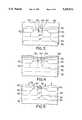
- FIG. 1shows a schematic cross-sectional view through part of an integrated circuit structure showing a bipolar transistor formed according to a known conventional prior art method
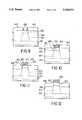
- FIGS. 2, 3, 4, 5, 6, 7, 8show a schematic cross-sectional view of part of an integrated circuit structure at successive stages in a method forming a bipolar transistor according to a first embodiment of the present invention
- FIGS. 9, 10, 11show a schematic cross-sectional view of part of an integrated circuit structure at successive stages in a method forming a bipolar transistor according to a second embodiment of the present invention.
- FIG. 12shows a schematic cross-sectional view showing a modification of the emitter structure of FIG. 11.
- FIG. 1A schematic cross-sectional view through a bipolar transistor 10 formed by a conventional known, prior art, double-polysilicon process is shown in FIG. 1, and comprises a substrate in the form of part of a silicon wafer 12 having formed therein a N+ well region 16 forming device islands isolated by a planarized field oxide layer 18.
- An underlying N+ layer 14forms a buried collector, with dielectric trench isolation 13.
- An extrinsic base region 17 and intrinsic base region 19are formed in the surface of the device well region 16.
- a first polysilicon layer 20is deposited overall, including over the device well 16, and is patterned to define an emitter opening 21.
- the first polysilicon layer 20forms the base contact electrodes to the extrinsic base region 17.
- Dielectric sidewall spacers 26 of oxideare formed on exposed sidewalls of base polysilicon surrounding the opening 21 defining the emitter contact region and a layer of dielectric 24, e.g. CVD silicon dioxide is then deposited overall.
- a second polysilicon layer 22is then deposited overall, including on the intrinsic base region 19 in the emitter opening to form an emitter-base-contact 21 within the opening.
- base and emitter contacts 28are formed to the first and second polysilicon layers by a conventional known method.
- a collector contact 29 to the N+ well region forming the collectoris provided, spaced laterally from the base contacts.
- N and Prefer to negatively and positively doped semiconductor regions, with + and ++ to indicate heavy and very heavy doping respectively; and - indicates light doping.
- a substrate for an integrated circuitis provided in the form of a semiconductor silicon wafer 32 having a heavily doped buried layer 34, for example a layer of As or Sb doped N+ type silicon, overlaid by a 0.5 ⁇ m to 1.0 ⁇ m thick layer of epitaxial silicon 36 lightly doped with N type dopant, e.g. 5 ⁇ 10 15 cm -3 in which is defined a device well region.
- the layers 34 and 36are formed by a conventional method, for example, by epitaxial growth or alternatively by MeV ion implantation.
- a more heavily doped N well 38is provided in the epitaxial layer 36, for example by implantation with N type ions at a dose in the ⁇ 5 ⁇ 10 16 cm -2 range, this implant being excluded from a device well region 36 in which a bipolar transistor is to be formed.
- the more heavily doped N well concentrationprovides for increasing the field threshold for the parasitic field oxide MOSFET or to serve as an appropriate well for CMOS transistors on the same die.
- the dopant concentrationis increased under the field oxide by the use of an N guard implant immediately prior to the field oxidation rather than during well formation.
- a conventional field isolation layer 40is formed, for example by a known fully recessed field oxide process to reduce surface topography for subsequent processing.
- a sacrificial layer 42is deposited overall.
- the sacrificial layer 42comprises a material which can withstand subsequent process steps for forming an emitter structure, as will be described, and may be etched selectively relative to the underlying substrate material.
- a well known suitable material for layer 42comprises a low density CVD silicon dioxide layer.
- the oxide layer 42is deposited overall, but it is not densified, as would be conventional, so that where the field isolation 40 is also silicon dioxide, the sacrificial layer is differentiated from the underlying field oxide layer 40 of silicon dioxide.
- plasma etching of the sacrificial oxide layer 42can then be performed with at least 2:1 selectivity relative to the underlying field oxide 40 using a conventional dry etching process, that is a plasma etch or reactive ion etch process.
- a conventional PE stepis performed to define an emitter opening 44 (FIG. 3), that is, a step of coating the wafer with photoresist 46, and patterning to expose a region 48 of the sacrificial layer 42 in the device well region for defining an opening.
- the exposed region 48 of the sacrificial layer 42is then etched by a conventional anisotropic etch process which is selective to the underlying silicon and to the field oxide outside the well region, to form a steep-sided opening 44 exposing the silicon surface 50 within the opening.
- a base implantcomprising for example a dose of ⁇ 2 ⁇ 10 13 cm -2 of ⁇ 20 keV boron ions, is performed to form a shallow intrinsic base region 52 in the surface of the well region within the opening.
- a local collector implantinto the underlying region 54, is then performed so that the two implants are self-aligned within the emitter opening 44.
- the latter implantcomprises, for example, a deep, i.e. high energy implant, of a dose of 5 ⁇ 10 12 cm -2 of 350 keV phosphorous ions.
- the local collector implantmay alternatively be performed before the base implant and annealed. The latter step allows for some lateral diffusion of the collector implant relative to the intrinsic base region, if desired.
- a conductive layer 58 of an emitter materialis provided within the emitter opening, for example, heavily doped polysilicon, formed by a conventional method.
- the polysilicon layer 58 forming the emitteris either in situ doped or deposited undoped and subsequently doped by ion implantation, as described below.
- the emitter layer 58is formed immediately after removing any native oxide formed on the exposed silicon surface 50 of the intrinsic base, e.g. by dipping in HF, so as to ensure a good contact between the emitter layer 58 and the underlying silicon surface 50.
- the layer 58When the layer of polysilicon 58 is deposited overall by a conventional method of CVD, the layer 58 must be thick enough to completely fill the emitter opening 44 defined in the oxide 42 without leaving a depression 45 in the growing surface of the polysilicon layer within the opening (FIG. 4).
- the polysilicon layer 58is then etched back and planarized, preferably by a step of chemical mechanical polishing, or by another known polysilicon etch process, for example reactive ion or plasma etching.
- an emitter structure 60 of polysiliconremains in the emitter opening 44 formed by the sacrificial layer 42 (FIG. 5), and forms the emitter-base junction 61 with the underlying intrinsic base region 52.
- Deposition of polysilicon by CVDprovides for running of the polysilicon layer 58 outside the device region over the field oxide, if required, e.g. for polysilicon structures of CMOS devices in a BiCMOS integrated circuit.
- An alternative method for forming the emitteris selective polysilicon growth, in which polysilicon 60 is grown selectively only in the emitter opening 44.
- the emitter layer 58When the emitter layer 58 is not heavily doped in situ during deposition, after filling the emitter opening 44 by formation of the emitter polysilicon structure, i.e. the "emitter stripe" 60, implantation of the emitter stripe 60 with a high dose of N type dopant, e.g. As, is performed.
- the polysilicon layer 58 in the emitter region 60should be thick enough to allow the implant to be performed without penetration of the implant ions through the polysilicon layer into the underlying base 52, and so that the emitter structure 60 is thick enough to sustain any loss during subsequent processing, such as salicidation of the surface region 62 for contact formation (FIG. 8).
- the thicknessmust be sufficient to provide high gain, that is to function as an excellent sink for back injected holes.
- a high dose implant into the polysilicon layeralso dopes the exposed deposited oxide 42, the layer 42 is sacrificial and is subsequently removed along with the excess dopant.
- a link implant in the base region 64 adjacent the emitteris provided to create a low resistance path between the intrinsic device, and the extrinsic base contact area 68 without affecting the performance of the intrinsic device in a deleterious manner.
- the link implantmay be performed after masking to leave an area 64 exposed in the device region 68 around the intrinsic base region, adjacent the emitter stripe 60.
- a low dose boron implantis provided in the exposed link region 64 of device well.
- a doping concentration of approximately equal to the base 52, or slightly higher and somewhat deeperis preferred.
- the implantis retrograde (see FIG. 8) away from the surface to reduce the local electric field (corner field) and improve the breakdown field of the emitter-base junction.
- Localized isolation for the emitter in the form of a dielectric sidewall spacer 66 adjacent the emitter region 60is then formed by conventional process steps, e.g. by deposition and anisotropic etching of a dielectric such as silicon dioxide (FIG. 7).
- the sidewall spacerprovides isolation of the emitter from the extrinsic base region thus ensuring current is concentrated through the emitter-base junction, to reduce or avoid leakage around the sides of the emitter.
- a standard extrinsic p+ implantis performed into the extrinsic base contact regions 68, followed by an anneal at high temperature to repair implant damage.
- the latter steps for dielectric sidewall spacer (SWS) formation, implantation and annealingmay be combined with appropriate CMOS steps for forming MOS devices, to reduce total process complexity.
- the subsequent "back end" processing steps for providing contact metallizationcomprise known processes, for example the metallization steps commonly used in CMOS processing.
- a thicker than conventional salicide layeris formed on the exposed emitter polysilicon layer 60.
- the thick salicide layer 70is provided to overcome emitter resistance debiasing which occurs when a significant voltage drop occurs between the contact and any point along the emitter stripe.
- a self-aligned metallizationsuch as selectively deposited tungsten, is preferred over a conventional aluminium alloy metallization.
- NPN PEto define emitter stripe region
- N-typelocal collector implant 5 ⁇ 10 12 cm -2 retrograde 350 keV into emitter stripe region
- heavily doped polysiliconmay alternatively be provided by CVD with in situ doping, rather than by ion implantation of undoped polysilicon.
- CVD polysiliconbeing formed by an established process, provides ease of use and manufacturability and is a preferred emitter material.
- provision of an emitter by selective growth of polysiliconis advantageous in allowing for growth selectively within the emitter opening. Thus etching back for removal of excess polysilicon by chemical mechanical polishing or a conventional etch back process is avoided.
- the process of the embodimentis also adaptable for forming silicon heterojunction bipolar transistors SiHBTs using alternative emitter or base materials, including high band gap emitter materials such as silicon carbide (SiC); a silicon germanium (SiGe) base, or alternative lower band gap materials.
- high band gap emitter materialssuch as silicon carbide (SiC); a silicon germanium (SiGe) base, or alternative lower band gap materials.
- SiCsilicon carbide
- SiGesilicon germanium
- a principle reason for a polysilicon base contact electrode in a double polysilicon processis to reduce the parasitic capacitance and resistance associated with the alignment overlap tolerance between levels.
- the use of a local collector implant and a light N well for the device regions of the transistorsubstantially reduces the parasitic capacitance and is sufficient for many applications. As shown in FIG.
- contact metallizationmay comprise for example, a local interconnect conductor 74 which is provided to move the base contact 78 out onto an adjacent field isolation area 40.
- This structureprovides a similar advantage for a single polysilicon process flow as a polysilicon base contact, without most of the disadvantages associated with the extra topography of a second polysilicon layer.
- the process of the embodimentprovides limited emitter contact area compared with known double-polysilicon processes, but the process avoids many of the manufacturability problems associated with highly non-planar topography of known double-polysilicon processes. Placement of the emitter contact may be a concern for manufacturability of a process if unrestricted contact placement is required in a standard process. Because there is a limited window for forming an emitter contact, if the sidewall spacer is formed of a dielectric material which is relatively etch resistant compared with silicon dioxide, e.g. tantalum oxide, or silicon nitride, there is some allowance for contact misregistration (i.e. relative registration error+contact width) when opening the emitter contact.
- the structureprovides for reduced parasitic capacitances and resistances. Lithographic registration errors, and critical dimensional variability between layers is reduced, particularly in the steps for emitter formation and base formation.
- the base, collector and link implantsallows more flexibility in the choice of these implants. Since the implants for the base region and the link region of the base contact region are completely independent, implants for each area can be separately optimized. The requirement for PE steps is reduced because one primary mask can provide all patterning for forming an emitter structure.
- the link implantmay be self-aligned with the emitter structure, or an additional mask may be used to define the link implant region, if required in a BiCMOS process. Thus, the process results in a cost reduction and yield improvement for bipolar transistors for BiCMOS ICs.
- a PNP bipolar transistor structuremay be provided by a complementary process to provide elements of opposite conductivity type, if required.
- a bipolar transistoris formed by steps as in the first embodiment, except that after defining an emitter opening in the sacrificial masking layer, sidewalls of the emitter opening are tapered.
- elements which are similar to those of the first embodimentare denoted by the same reference numeral incremented by 100.
- the process stepsare similar to those of the first embodiment except that the sidewalls of the opening 144 are tapered by forming dielectric sidewall spacers 165 within the opening after formation of the intrinsic base region 152 by ion implantation.
- the sidewall spacers 156provide a self-aligned layer of dielectric for isolation of the emitter layer (FIG. 9).
- the edges of the emitter structure 160are isolated from the extrinsic base region 164 by the sidewall spacers 165.
- the tapered sidewall spacers 165result in formation of a tapered emitter structure 160 which has a narrow base-emitter contact area 161, and which widens and forms a larger emitter contact region 170 on the exposed surface of the emitter structure.
- the emitter-base junction widthis reduced, satisfactory contact area to the emitter is provided.
- FIG. 12A modification of the emitter structure of the second embodiment is shown in FIG. 12, in which sidewall spacers 165 are formed only in the lower part of the opening in the sacrificial layer.
- a self-aligned intrinsic base regionis provided by selective epitaxial growth of a base material within the opening in the sacrificial layer, either before or after formation of the sidewall spacers.
Landscapes
- Bipolar Transistors (AREA)
Abstract
Description
Claims (27)
Priority Applications (2)
| Application Number | Priority Date | Filing Date | Title |
|---|---|---|---|
| US08/001,706US5320972A (en) | 1993-01-07 | 1993-01-07 | Method of forming a bipolar transistor |
| US08/158,544US5428243A (en) | 1993-01-07 | 1993-11-29 | Bipolar transistor with a self-aligned heavily doped collector region and base link regions. |
Applications Claiming Priority (1)
| Application Number | Priority Date | Filing Date | Title |
|---|---|---|---|
| US08/001,706US5320972A (en) | 1993-01-07 | 1993-01-07 | Method of forming a bipolar transistor |
Related Child Applications (1)
| Application Number | Title | Priority Date | Filing Date |
|---|---|---|---|
| US08/158,544DivisionUS5428243A (en) | 1993-01-07 | 1993-11-29 | Bipolar transistor with a self-aligned heavily doped collector region and base link regions. |
Publications (1)
| Publication Number | Publication Date |
|---|---|
| US5320972Atrue US5320972A (en) | 1994-06-14 |
Family
ID=21697419
Family Applications (2)
| Application Number | Title | Priority Date | Filing Date |
|---|---|---|---|
| US08/001,706Expired - LifetimeUS5320972A (en) | 1993-01-07 | 1993-01-07 | Method of forming a bipolar transistor |
| US08/158,544Expired - LifetimeUS5428243A (en) | 1993-01-07 | 1993-11-29 | Bipolar transistor with a self-aligned heavily doped collector region and base link regions. |
Family Applications After (1)
| Application Number | Title | Priority Date | Filing Date |
|---|---|---|---|
| US08/158,544Expired - LifetimeUS5428243A (en) | 1993-01-07 | 1993-11-29 | Bipolar transistor with a self-aligned heavily doped collector region and base link regions. |
Country Status (1)
| Country | Link |
|---|---|
| US (2) | US5320972A (en) |
Cited By (19)
| Publication number | Priority date | Publication date | Assignee | Title |
|---|---|---|---|---|
| US5432104A (en)* | 1993-10-07 | 1995-07-11 | Nec Corporation | Method for fabricating a vertical bipolar transistor with reduced parasitic capacitance between base and collector regions |
| US5444004A (en)* | 1994-04-13 | 1995-08-22 | Winbond Electronics Corporation | CMOS process compatible self-alignment lateral bipolar junction transistor |
| US5496746A (en)* | 1991-10-23 | 1996-03-05 | Microsystems Engineering, Inc. | Method for fabricating a bipolar junction transistor exhibiting improved beta and punch-through characteristics |
| US5516710A (en)* | 1994-11-10 | 1996-05-14 | Northern Telecom Limited | Method of forming a transistor |
| US5596215A (en)* | 1995-06-08 | 1997-01-21 | Taiwan Semiconductor Manufacturing Company | Method to improve buried contact resistance |
| EP0887852A2 (en)* | 1997-06-25 | 1998-12-30 | Siemens Aktiengesellschaft | Improved silica stain test structures and methods therefor |
| US5904552A (en)* | 1997-02-25 | 1999-05-18 | Motorola, Inc. | Method of resistless patterning of a substrate for implantation |
| US5986323A (en)* | 1994-10-28 | 1999-11-16 | Consorzio Per La Ricerca Sulla Microelettronica Nel Mezzogiorno | High-frequency bipolar transistor structure |
| WO2001039274A1 (en)* | 1999-11-26 | 2001-05-31 | Infineon Technologies Ag | Retrograde doped buried layer transistor and method for producing the same |
| US6426265B1 (en) | 2001-01-30 | 2002-07-30 | International Business Machines Corporation | Incorporation of carbon in silicon/silicon germanium epitaxial layer to enhance yield for Si-Ge bipolar technology |
| US6444536B2 (en)* | 1999-07-08 | 2002-09-03 | Agere Systems Guardian Corp. | Method for fabricating bipolar transistors |
| US6492237B2 (en)* | 2001-02-12 | 2002-12-10 | Maxim Integrated Products, Inc. | Method of forming an NPN device |
| US6569744B2 (en) | 2001-06-15 | 2003-05-27 | Agere Systems Inc. | Method of converting a metal oxide semiconductor transistor into a bipolar transistor |
| US20030189239A1 (en)* | 2002-04-09 | 2003-10-09 | Alexander Kalnitsky | Self-aligned NPN transistor with raised extrinsic base |
| US6649482B1 (en)* | 2001-06-15 | 2003-11-18 | National Semiconductor Corporation | Bipolar transistor with a silicon germanium base and an ultra small self-aligned polysilicon emitter and method of forming the transistor |
| US6784065B1 (en) | 2001-06-15 | 2004-08-31 | National Semiconductor Corporation | Bipolar transistor with ultra small self-aligned polysilicon emitter and method of forming the transistor |
| US20050184359A1 (en)* | 2004-02-25 | 2005-08-25 | International Business Machines Corporation | Structure and method of self-aligned bipolar transistor having tapered collector |
| US7087979B1 (en) | 2001-06-15 | 2006-08-08 | National Semiconductor Corporation | Bipolar transistor with an ultra small self-aligned polysilicon emitter |
| US20080026552A1 (en)* | 2006-07-31 | 2008-01-31 | Martin Gerhardt | Method of enhancing lithography capabilities during gate formation in semiconductors having a pronounced surface topography |
Families Citing this family (8)
| Publication number | Priority date | Publication date | Assignee | Title |
|---|---|---|---|---|
| JPH10163435A (en)* | 1996-11-29 | 1998-06-19 | Mitsubishi Electric Corp | Semiconductor memory device and method of manufacturing the same |
| KR100355034B1 (en)* | 1999-07-15 | 2002-10-05 | 삼성전자 주식회사 | Semiconductor device with SEG layer and Method for isolating thereof |
| US6630699B1 (en) | 2000-08-31 | 2003-10-07 | Lucent Technologies, Inc. | Transistor device having an isolation structure located under a source region, drain region and channel region and a method of manufacture thereof |
| US6410975B1 (en)* | 2000-09-01 | 2002-06-25 | Newport Fab, Llc | Bipolar transistor with reduced base resistance |
| DE10142690A1 (en)* | 2001-08-31 | 2003-03-27 | Infineon Technologies Ag | Contacting the emitter contact of a semiconductor device |
| US6656811B2 (en)* | 2001-12-21 | 2003-12-02 | Texas Instruments Incorporated | Carbide emitter mask etch stop |
| US7288829B2 (en)* | 2004-11-10 | 2007-10-30 | International Business Machines Corporation | Bipolar transistor with self-aligned retrograde extrinsic base implant profile and self-aligned silicide |
| US8841750B2 (en) | 2012-07-18 | 2014-09-23 | International Business Machines Corporation | Local wiring for a bipolar junction transistor including a self-aligned emitter region |
Citations (9)
| Publication number | Priority date | Publication date | Assignee | Title |
|---|---|---|---|---|
| JPS6471166A (en)* | 1987-09-10 | 1989-03-16 | Sharp Kk | Manufacture of tantalum oxide thin film |
| US4988632A (en)* | 1990-01-02 | 1991-01-29 | Motorola, Inc. | Bipolar process using selective silicon deposition |
| US5034351A (en)* | 1990-10-01 | 1991-07-23 | Motorola, Inc. | Process for forming a feature on a substrate without recessing the surface of the substrate |
| US5055419A (en)* | 1985-03-23 | 1991-10-08 | Stc, Plc | Method of manufacturing a bipolar transistor |
| US5057455A (en)* | 1989-11-30 | 1991-10-15 | At&T Bell Laboratories | Formation of integrated circuit electrodes |
| US5064774A (en)* | 1991-02-19 | 1991-11-12 | Motorola, Inc. | Self-aligned bipolar transistor process |
| US5169794A (en)* | 1991-03-22 | 1992-12-08 | National Semiconductor Corporation | Method of fabrication of pnp structure in a common substrate containing npn or MOS structures |
| US5194926A (en)* | 1991-10-03 | 1993-03-16 | Motorola Inc. | Semiconductor device having an inverse-T bipolar transistor |
| US5208169A (en)* | 1991-06-28 | 1993-05-04 | Texas Instruments Incorporated | Method of forming high voltage bipolar transistor for a BICMOS integrated circuit |
Family Cites Families (3)
| Publication number | Priority date | Publication date | Assignee | Title |
|---|---|---|---|---|
| JP2728671B2 (en)* | 1988-02-03 | 1998-03-18 | 株式会社東芝 | Manufacturing method of bipolar transistor |
| US5302535A (en)* | 1991-09-20 | 1994-04-12 | Nec Corporation | Method of manufacturing high speed bipolar transistor |
| WO1993017461A1 (en)* | 1992-02-25 | 1993-09-02 | Microunity Systems Engineering, Inc. | Bipolar junction transistor exhibiting suppressed kirk effect |
- 1993
- 1993-01-07USUS08/001,706patent/US5320972A/ennot_activeExpired - Lifetime
- 1993-11-29USUS08/158,544patent/US5428243A/ennot_activeExpired - Lifetime
Patent Citations (9)
| Publication number | Priority date | Publication date | Assignee | Title |
|---|---|---|---|---|
| US5055419A (en)* | 1985-03-23 | 1991-10-08 | Stc, Plc | Method of manufacturing a bipolar transistor |
| JPS6471166A (en)* | 1987-09-10 | 1989-03-16 | Sharp Kk | Manufacture of tantalum oxide thin film |
| US5057455A (en)* | 1989-11-30 | 1991-10-15 | At&T Bell Laboratories | Formation of integrated circuit electrodes |
| US4988632A (en)* | 1990-01-02 | 1991-01-29 | Motorola, Inc. | Bipolar process using selective silicon deposition |
| US5034351A (en)* | 1990-10-01 | 1991-07-23 | Motorola, Inc. | Process for forming a feature on a substrate without recessing the surface of the substrate |
| US5064774A (en)* | 1991-02-19 | 1991-11-12 | Motorola, Inc. | Self-aligned bipolar transistor process |
| US5169794A (en)* | 1991-03-22 | 1992-12-08 | National Semiconductor Corporation | Method of fabrication of pnp structure in a common substrate containing npn or MOS structures |
| US5208169A (en)* | 1991-06-28 | 1993-05-04 | Texas Instruments Incorporated | Method of forming high voltage bipolar transistor for a BICMOS integrated circuit |
| US5194926A (en)* | 1991-10-03 | 1993-03-16 | Motorola Inc. | Semiconductor device having an inverse-T bipolar transistor |
Non-Patent Citations (6)
| Title |
|---|
| A High Speed Bipolar Technology Featuring Self Aligned Single Poly Base and Submicrometer Emitter Contacts, IEEE Electron Device Letters, vol., 11, No. 9, Sep. 1990, pp. 412 414, Huang et al.* |
| A High-Speed Bipolar Technology Featuring Self-Aligned Single-Poly Base and Submicrometer Emitter Contacts, IEEE Electron Device Letters, vol., 11, No. 9, Sep. 1990, pp. 412-414, Huang et al. |
| High Speed Polysilicon Emitter Base Bipolar Transistor, IEEE Electron Device Letters, vol., EDL 7, No. 12, Dec. 1986, pp. 658 661, Park et al.* |
| High-Speed Polysilicon Emitter-Base Bipolar Transistor, IEEE Electron Device Letters, vol., EDL-7, No. 12, Dec. 1986, pp. 658-661, Park et al. |
| Wolf, S., et al., Silicon Processing, vol. 1, 1986, Lattice Press, pp. 182 195.* |
| Wolf, S., et al., Silicon Processing, vol. 1, 1986, Lattice Press, pp. 182-195. |
Cited By (33)
| Publication number | Priority date | Publication date | Assignee | Title |
|---|---|---|---|---|
| US5496746A (en)* | 1991-10-23 | 1996-03-05 | Microsystems Engineering, Inc. | Method for fabricating a bipolar junction transistor exhibiting improved beta and punch-through characteristics |
| US5432104A (en)* | 1993-10-07 | 1995-07-11 | Nec Corporation | Method for fabricating a vertical bipolar transistor with reduced parasitic capacitance between base and collector regions |
| US5444004A (en)* | 1994-04-13 | 1995-08-22 | Winbond Electronics Corporation | CMOS process compatible self-alignment lateral bipolar junction transistor |
| US5986323A (en)* | 1994-10-28 | 1999-11-16 | Consorzio Per La Ricerca Sulla Microelettronica Nel Mezzogiorno | High-frequency bipolar transistor structure |
| US5516710A (en)* | 1994-11-10 | 1996-05-14 | Northern Telecom Limited | Method of forming a transistor |
| US5596215A (en)* | 1995-06-08 | 1997-01-21 | Taiwan Semiconductor Manufacturing Company | Method to improve buried contact resistance |
| US5904552A (en)* | 1997-02-25 | 1999-05-18 | Motorola, Inc. | Method of resistless patterning of a substrate for implantation |
| EP0887852A2 (en)* | 1997-06-25 | 1998-12-30 | Siemens Aktiengesellschaft | Improved silica stain test structures and methods therefor |
| US6444536B2 (en)* | 1999-07-08 | 2002-09-03 | Agere Systems Guardian Corp. | Method for fabricating bipolar transistors |
| WO2001039274A1 (en)* | 1999-11-26 | 2001-05-31 | Infineon Technologies Ag | Retrograde doped buried layer transistor and method for producing the same |
| US6806152B1 (en) | 1999-11-26 | 2004-10-19 | Infineon Technologies Ag | Retrograde doped buried layer transistor and method for producing the same |
| US6426265B1 (en) | 2001-01-30 | 2002-07-30 | International Business Machines Corporation | Incorporation of carbon in silicon/silicon germanium epitaxial layer to enhance yield for Si-Ge bipolar technology |
| US7713829B2 (en) | 2001-01-30 | 2010-05-11 | International Business Machines Corporation | Incorporation of carbon in silicon/silicon germanium epitaxial layer to enhance yield for Si-Ge bipolar technology |
| US20080124881A1 (en)* | 2001-01-30 | 2008-05-29 | International Business Machines Corporation | INCORPORATION OF CARBON IN SILICON/SILICON GERMANIUM EPITAXIAL LAYER TO ENHANCE YIELD FOR Si-Ge BIPOLAR TECHNOLOGY |
| US7173274B2 (en) | 2001-01-30 | 2007-02-06 | International Business Machines Corporation | Incorporation of carbon in silicon/silicon germanium epitaxial layer to enhance yield for Si-Ge bipolar technology |
| US20050054171A1 (en)* | 2001-01-30 | 2005-03-10 | International Business Machines Corporation | Incorporation of carbon in silicon/silicon germanium epitaxial layer to enhance yield for Si-Ge bipolar technology |
| US6815802B2 (en) | 2001-01-30 | 2004-11-09 | International Business Machines Corporation | Incorporation of carbon in silicon/silicon germanium epitaxial layer to enhance yield for Si-Ge bipolar technology |
| US6492237B2 (en)* | 2001-02-12 | 2002-12-10 | Maxim Integrated Products, Inc. | Method of forming an NPN device |
| US7087979B1 (en) | 2001-06-15 | 2006-08-08 | National Semiconductor Corporation | Bipolar transistor with an ultra small self-aligned polysilicon emitter |
| US6784065B1 (en) | 2001-06-15 | 2004-08-31 | National Semiconductor Corporation | Bipolar transistor with ultra small self-aligned polysilicon emitter and method of forming the transistor |
| US6753234B1 (en) | 2001-06-15 | 2004-06-22 | National Semiconductor Corporation | Method of forming the silicon germanium base of a bipolar transistor |
| US6649482B1 (en)* | 2001-06-15 | 2003-11-18 | National Semiconductor Corporation | Bipolar transistor with a silicon germanium base and an ultra small self-aligned polysilicon emitter and method of forming the transistor |
| US6569744B2 (en) | 2001-06-15 | 2003-05-27 | Agere Systems Inc. | Method of converting a metal oxide semiconductor transistor into a bipolar transistor |
| US20030189239A1 (en)* | 2002-04-09 | 2003-10-09 | Alexander Kalnitsky | Self-aligned NPN transistor with raised extrinsic base |
| US6767798B2 (en) | 2002-04-09 | 2004-07-27 | Maxim Integrated Products, Inc. | Method of forming self-aligned NPN transistor with raised extrinsic base |
| US20040126978A1 (en)* | 2002-04-09 | 2004-07-01 | Alexander Kalnitsky | Self-aligned NPN transistor with raised extrinsic base |
| US7026666B2 (en) | 2002-04-09 | 2006-04-11 | Maxim Integrated Products, Inc. | Self-aligned NPN transistor with raised extrinsic base |
| US20050184359A1 (en)* | 2004-02-25 | 2005-08-25 | International Business Machines Corporation | Structure and method of self-aligned bipolar transistor having tapered collector |
| US7425754B2 (en)* | 2004-02-25 | 2008-09-16 | International Business Machines Corporation | Structure and method of self-aligned bipolar transistor having tapered collector |
| US20080318373A1 (en)* | 2004-02-25 | 2008-12-25 | International Business Machines Corporation | Method of fabricating self-aligned bipolar transistor having tapered collector |
| US7615457B2 (en)* | 2004-02-25 | 2009-11-10 | International Business Machines Corporation | Method of fabricating self-aligned bipolar transistor having tapered collector |
| US20080026552A1 (en)* | 2006-07-31 | 2008-01-31 | Martin Gerhardt | Method of enhancing lithography capabilities during gate formation in semiconductors having a pronounced surface topography |
| US8101512B2 (en)* | 2006-07-31 | 2012-01-24 | Globalfoundries Inc. | Method of enhancing lithography capabilities during gate formation in semiconductors having a pronounced surface topography |
Also Published As
| Publication number | Publication date |
|---|---|
| US5428243A (en) | 1995-06-27 |
Similar Documents
| Publication | Publication Date | Title |
|---|---|---|
| US5320972A (en) | Method of forming a bipolar transistor | |
| US5516710A (en) | Method of forming a transistor | |
| US6287930B1 (en) | Methods of forming bipolar junction transistors having trench-based base electrodes | |
| US4868135A (en) | Method for manufacturing a Bi-CMOS device | |
| US4318751A (en) | Self-aligned process for providing an improved high performance bipolar transistor | |
| US5439833A (en) | Method of making truly complementary and self-aligned bipolar and CMOS transistor structures with minimized base and gate resistances and parasitic capacitance | |
| US6794237B2 (en) | Lateral heterojunction bipolar transistor | |
| US5100813A (en) | Method of manufacturing bipolar transistor | |
| WO1994028577A2 (en) | Method of producing a structure with narrow line width and devices obtained | |
| US5970333A (en) | Dielectric isolation bipolar transistor | |
| US7456070B2 (en) | Method of fabricating a bipolar transistor with high breakdown voltage collector | |
| US7968416B2 (en) | Integrated circuit arrangement with NPN and PNP bipolar transistors and corresponding production method | |
| US20070161173A1 (en) | Process to integrate fabrication of bipolar devices into a CMOS process flow | |
| US4980738A (en) | Single polysilicon layer transistor with reduced emitter and base resistance | |
| EP0281235B1 (en) | Bipolar transistor fabrication utilizing cmos techniques | |
| US6563147B1 (en) | HBT with a SiGe base region having a predetermined Ge content profile | |
| US5516708A (en) | Method of making single polysilicon self-aligned bipolar transistor having reduced emitter-base junction | |
| US5882976A (en) | Method of fabricating a self-aligned double polysilicon NPN transistor with poly etch stop | |
| JPH10189789A (en) | Bipolar transistors and capacitors | |
| JPH09116039A (en) | Method for manufacturing BiCMOS device | |
| EP0036499A1 (en) | A polysilicon-base self-aligned bipolar transistor process | |
| US5747374A (en) | Methods of fabricating bipolar transistors having separately formed intrinsic base and link-up regions | |
| US6790736B2 (en) | Method for manufacturing and structure of semiconductor device with polysilicon definition structure | |
| US5904536A (en) | Self aligned poly emitter bipolar technology using damascene technique | |
| US6331727B1 (en) | Semiconductor device and method of fabricating the same |
Legal Events
| Date | Code | Title | Description |
|---|---|---|---|
| AS | Assignment | Owner name:NORTHERN TELECOM LIMITED, CANADA Free format text:ASSIGNMENT OF ASSIGNORS INTEREST.;ASSIGNOR:WYLIE, IAN W.;REEL/FRAME:006410/0283 Effective date:19921210 | |
| STCF | Information on status: patent grant | Free format text:PATENTED CASE | |
| FPAY | Fee payment | Year of fee payment:4 | |
| AS | Assignment | Owner name:NORTEL NETWORKS CORPORATION, CANADA Free format text:CHANGE OF NAME;ASSIGNOR:NORTHERN TELECOM LIMITED;REEL/FRAME:010567/0001 Effective date:19990429 | |
| AS | Assignment | Owner name:NORTEL NETWORKS LIMITED, CANADA Free format text:CHANGE OF NAME;ASSIGNOR:NORTEL NETWORKS CORPORATION;REEL/FRAME:011195/0706 Effective date:20000830 Owner name:NORTEL NETWORKS LIMITED,CANADA Free format text:CHANGE OF NAME;ASSIGNOR:NORTEL NETWORKS CORPORATION;REEL/FRAME:011195/0706 Effective date:20000830 | |
| AS | Assignment | Owner name:STMICROELECTRONICS N.V., SWITZERLAND Free format text:ASSIGNMENT OF ASSIGNORS INTEREST;ASSIGNOR:NORTEL NETWORKS LIMITED;REEL/FRAME:011967/0805 Effective date:20010525 | |
| FPAY | Fee payment | Year of fee payment:8 | |
| FEPP | Fee payment procedure | Free format text:PAYOR NUMBER ASSIGNED (ORIGINAL EVENT CODE: ASPN); ENTITY STATUS OF PATENT OWNER: LARGE ENTITY | |
| FPAY | Fee payment | Year of fee payment:12 |