US5315534A - Computer process for interconnecting logic circuits utilizing softwire statements - Google Patents
Computer process for interconnecting logic circuits utilizing softwire statementsDownload PDFInfo
- Publication number
- US5315534A US5315534AUS07/720,356US72035691AUS5315534AUS 5315534 AUS5315534 AUS 5315534AUS 72035691 AUS72035691 AUS 72035691AUS 5315534 AUS5315534 AUS 5315534A
- Authority
- US
- United States
- Prior art keywords
- softwire
- jog
- points
- layout
- statement
- Prior art date
- Legal status (The legal status is an assumption and is not a legal conclusion. Google has not performed a legal analysis and makes no representation as to the accuracy of the status listed.)
- Expired - Lifetime
Links
Images


Classifications
- G—PHYSICS
- G06—COMPUTING OR CALCULATING; COUNTING
- G06F—ELECTRIC DIGITAL DATA PROCESSING
- G06F30/00—Computer-aided design [CAD]
- G06F30/30—Circuit design
- G06F30/39—Circuit design at the physical level
- G06F30/394—Routing
Definitions
- This inventionrelates to Computer Aided Design (CAD) systems; and more particularly, it relates to CAD software programs which lay out physical interconnections for logic circuits on an integrated circuit substrate.
- CADComputer Aided Design
- the above logic circuitscan be a variety of logic cells and the above substrate can be a single semiconductor chip.
- the logic circuitscan be several integrated circuit chips and the substrate can be a multichip ceramic wafer.
- a library of many different types of logic circuitsis provided; and from that library, certain logic circuits are selected for placement on each particular substrate.
- a logic cell librarycontains over one hundred different types of cells such as various types of NAND gates, NOR gates, AND gates, OR gates, multiplexers, latches, flip-flops, etc.; and several thousand of such cells are usually placed on a single semiconductor chip.
- Each logic circuithas one or more input terminals and one or more output terminals; and, those terminals need to be selectively interconnected on the substrate.
- a listing of which terminals are to be connected togetheris provided by a netlist. Given the netlist and the list of circuits that are selected from the library, the problem arises of precisely where on the substrate each of the selected circuits and each of the circuit interconnections should be physically located. As the number of circuits plus the number of interconnections increases, solving the above "layout" problem becomes more and more tedious.
- the above layout problemwas solved as follows. To begin, a design engineer or technician assigned specific locations on the substrate to each of the logic circuits. This was done by defining a fixed x, y coordinate system on the substrate, and by giving specific x and y dimensional coordinates to each of the circuits. Thereafter, a CAD software program received as an input the x and y dimensional coordinates of each of the circuits along with the netlist; and as an output the CAD program provided specific x and y dimensional coordinates to each of the circuit interconnections. In performing this task, the CAD program performed a global routing step in which certain open channels were found for each interconnection, and it performed a detailed routing step in which specific x, y dimensional coordinates were assigned to each interconnection in its channel.
- a symbolic layout CAD systemWith the symbolic layout CAD system, a design engineer or technician graphically locates the logic circuits by electronically arranging various symbols that represent those circuits on CRT screen. Typically, the symbols are moved on the CRT screen by means of an electromechanical "mouse". Also the design engineer/technician uses the mouse to draw lines on the CRT screen from one symbol to another, as a representation of physical conductors between the logic circuits. Then, after the desired arrangement of the symbols and lines is made, another CAD program called a "Compactor" assigns dimensional x and y coordinates to each of the circuits and conductors that correspond to symbols and lines.
- actorassigns dimensional x and y coordinates to each of the circuits and conductors that correspond to symbols and lines.
- a primary object of the inventionis to provide a novel CAD process in which the logic circuits can be moved on the substrate and the layout of the interconnections can be obtained without repeating all of the layout steps from the scratch.
- a computer processwhich interconnects logic circuit on an integrated circuit substrate by generating a single softwire statement for each interconnection, and by thereafter utilizing the softwire statements to generate multiple physical layouts for each interconnection.
- a "softwire statement”is herein meant a computer-generated statement which specifies and establishes a route for an interconnection from one terminal of a logic circuit to another terminal as a series of conductive segments which extend in certain directions between relative jog points that are referenced to blockages on the substrate. These blockages include the logic circuits themselves and any pre-existing interconnections.
- the jog pointsmove as the blockages move and the softwire statements of the interconnections remain unchanged.
- a layout for the physical interconnections between the logic circuits at their new locationis obtained by simply substituting into the softwire statements the dimensional coordinates of the blockages to which the jog points in the statements are referenced.
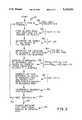
- FIG. 1illustrates a data processing system which performs a CAD layout process in accordance with the invention
- FIG. 2illustrates the steps of the CAD layout process which the FIG. 1 system performs
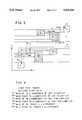
- FIG. 3shows an interconnection that is being formed on a chip in accordance with the process of FIG. 2;
- FIG. 4illustrates a softwire statement that is generated by the process of FIG. 2 and which establishes various layouts for the FIG. 3 interconnection;
- FIGS. 5 and 6illustrate two different physical layouts that are established by the softwire statement of FIG. 4;
- FIG. 7illustrates several classes of interconnections which may occur on a substrate.
- FIGS. 8A and 8Blist respective softwire statements that establish various physical layouts for the interconnection classes of FIG. 7.
- FIG. 1shows a data processing system which operates to interconnect logic circuits on an integrated circuit substrate in accordance with the invention.
- This data processing systemincludes a digital computer 10, an instruction memory 11, several data files 12-16, and an output file 17 in which softwire statements are listed. All of these components are interconnected via buses 18a-18c, as shown.
- File 12is a library of each type of logic circuit that is selectively disposed on the substrate.
- the librarydescribes the physical makeup of various logic cells that are integrated into a single semiconductor chip.
- the librarydescribes the physical makeup of various semiconductor chips that are mounted on a ceramic multi-chip wafer.
- File 13identifies all of the logic circuits that are selected from the library 12 and placed on the substrate, and it identifies the locations of those circuits on the substrate.
- File 13can be generated in any fashion such as by a hand layout or by any pre-existing CAD program.
- Each logic circuithas certain input/output terminals, and those terminals which are to be interconnected are identified by a netlist file 14.
- Any pre-existing interconnections for the logic circuits of file 13are contained in file 15.
- a set of values for certain layout parameters CIS, IIS, and IW for the softwire interconnections,is contained in file 16.
- CISis a minimum logic circuit to interconnection spacing
- IISis a minimum interconnection to interconnection spacing
- IWis a minimum interconnection line width.
- a computer program 20Stored in the instruction memory 11 is a computer program 20 which interconnects the logic circuits on the substrate by directing the computer 10 to receive and process the data in the files 12-16. As one intermediate result of that processing, computer 10 produces a listing of softwire statements in the output file 17. All of the process steps that are performed by computer 10 in response to the program 20 are shown in FIG. 2. Also, specific examples of the FIG. 2 process steps are shown in FIG's. 3 and 4.
- a pair of terminals which are to be interconnectedare selected from the netlist 14.
- An example of this stepis shown in FIG. 3 wherein the terminals that are to be interconnected are shown as M1 and N1 on a logic circuits M and N.
- step 20ban open space on the substrate is found which goes from one of the above selected terminals to the other. This open space is the "global" route for the softwire that is to be generated.
- the open spaceis bordered by several logic circuits A-E and by one pre-existing interconnection that is labelled "FOO".
- FOOpre-existing interconnection
- step 20cthe total number of jog points to be used is determined; and, in the example of FIG. 3, there are five jog points JP1-JP5.
- step 20devery other jog point is referenced to a respective blockage.
- jog point JP2is referenced to logic circuit A
- jog point JP4is referenced to the second segment F002 of wire F00.
- step 20ex and y coordinates of the above alternate jog points are expressed in terms of the layout parameters relative to their respective blockage.
- a bris the bottom right corner of a logic circuit A;
- F002 bris the bottom right corner of the second segment of wire F00; and
- CIS, IIS, and IWare the previously defined layout parameters.
- a softwire statementis generated in the output file 17.
- This statementestablishes an interconnection between the selected pair of terminals as a series of conductor segments that extend in the x and y directions from the above expressed coordinates of the alternate jog points.
- Such a softwire statement for the example of FIG. 3is given in FIG. 4.
- the interconnectionconsists of a total of six segments S1-S6.
- Each segment of the softwire statement from step 20fconstitutes a blockage for any additional terminals that are to be interconnected. This is indicated by step 20g.
- Each blockageis stored in file 15 as either a physical wire with fixed dimensional coordinates or with relative coordinates. And, for each such pair of terminals, the steps 20a-20g are repeated.
- step 20ieach of the expressions for the jog points in the softwire statement listing is evaluated by substituting the specific dimensional co-ordinates of the blockages from file 13 and the specific dimensional values of the layout parameters from file 16 into the softwire statements. Conductors having the resulting dimensional coordinates are displayed on a CRT screen and/or plotted on paper; and they are added to file 15. Thereafter, an actual integrated circuit having the displayed layout can be fabricated from the dimensional data in files 13 and 15 by any conventional integrated circuit fabrication process.
- a primary feature of the FIG. 2 processis that the location of the jog points in the softwire statements are expressed in relative terms with respect to various blockages, rather then in terms of fixed dimensional x, y coordinates.
- segment #1is referenced to the bottom right corner of logic circuit A; and segment #3 is referenced to the bottom right corner of blockage F002. Consequently, logic circuit A and/or wire F00 can be moved from one specific location to another; and so long as additional jog points are not introduced into the M1-N1 interconnection, the softwire statement of FIG. 4 remains unchanged.
- the steps of generating the softwire statementdo not need to be repeated. All that needs to be done is to re-evaluate the previously generated FIG. 4 statement.
- FIG. 2 processAnother feature of the FIG. 2 process is that the jog points in the softwire list are expressed in terms of layout parameters CIS, IIS, and IW rather then specific dimensional values for those parameters. Consequently, the fabrication process that builds the actual logic circuits and their interconnections can be modified (e.g., upgraded) without changing the softwire statements. Thus, to obtain dimensional coordinates of the interconnections after such a fabrication process upgrade, the previously generated softwire statement need only be re-evaluated.
- FIG. 5one particular physical layout for the M1-N1 interconnection is plotted between the logic circuits A-E and wire F00 in accordance with the softwire statement of FIG. 4.
- FIG. 6is a modification of the FIG. 5 layout in which logic circuit A is moved to a new location A'; logic circuit C is increased in size as shown by C'; wire F00 is stretched to accommodate the increased size of logic circuit C'; and the magnitude of the layout parameters CIS and IIS are decreased.
- each of the above modificationscauses the dimensional coordinates of the M1-N1 interconnection to change.
- the softwire statement of the FIG. 6 interconnection and the softwire statement of the FIG. 5 interconnectionare exactly the same.
- one particular layoutsuch as FIG. 5
- another particular layoutsuch as FIG. 6
- generating all of the various layoutscan account for over fifty percent of the total design time; and thus the time and money which the present invention saves can be substantial.
- the M1-N1 interconnectionillustrates just one particular class of interconnections (herein called class #1) that can be established by a softwire statement.
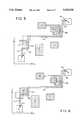
- classes #2-#8classes of interconnections that can also be established by a softwire statement are illustrated in FIG. 7.
- interconnectionsare labelled I1, I2, I3, etc.; blockages for the interconnection are labelled B1, B2, B3, etc.; source terminals for the interconnections are labelled s1, s2, etc.; and destination terminals for the interconnections are labelled d1, d2, etc.
- All of the interconnections of classes 1-4have a "vertically preferred" route from their source to their destination.
- a vertically preferred routeis meant a route which goes in the y direction rather then the x direction so long as the interconnection can stay within its open space.
- all of the interconnections of classes 5-8have a "horizontally preferred" route from the source to the destination terminal.
- a horizontally preferred routeis meant a route which goes in the x direction rather then the y direction so long as the interconnection can stay within its open space.
- the destination terminalis to the right and above the source terminal; in classes 2 and 6, the destination terminal is to the right and below the source terminal; in classes 3 and 7, the destination terminal is to the left and below the source terminal; and in classes 4 and 8, the destination terminal is to the left and above the source terminal.
- reference numerals 30-1 thru 30-16identify the particular corner of the blockages to which the jog points in the interconnections I1-I8 are referenced.
- the jog pointsare referenced to the bottom right corner of the blockages; for classes 3 and 5, the jog points are referenced to the top left corner of the blockages; for classes number 2 and 8, the jog points are referenced to the top right corner of the blockages; and for classes 4 and 6, the jog points are referenced to the bottom left corner of the blockages.
- the softwire statementscan be generated such that the interconnections that they establish include all or just some of the interconnection classes of FIG. 8.
- softwire statementsare generated such that they establish interconnections which have only a vertically preferred route (classes 1-4).
- softwire statementsare generated such that they establish interconnections which have only a horizontally preferred route (classes 5-8).
- the resulting interconnectionsare limited to classes 1, 2, 7, and 8.
- the resulting interconnectionsare limited to classes 3, 4, 5, and 6.
- FIG. 2 processcan be changed such that step 20 i immediately follows step 20 f .
- step 20 iimmediately follows step 20 f .
Landscapes
- Engineering & Computer Science (AREA)
- Computer Hardware Design (AREA)
- Physics & Mathematics (AREA)
- Theoretical Computer Science (AREA)
- Computer Networks & Wireless Communication (AREA)
- Evolutionary Computation (AREA)
- Geometry (AREA)
- General Engineering & Computer Science (AREA)
- General Physics & Mathematics (AREA)
- Design And Manufacture Of Integrated Circuits (AREA)
Abstract
Description
Claims (12)
Priority Applications (1)
| Application Number | Priority Date | Filing Date | Title |
|---|---|---|---|
| US07/720,356US5315534A (en) | 1991-06-25 | 1991-06-25 | Computer process for interconnecting logic circuits utilizing softwire statements |
Applications Claiming Priority (1)
| Application Number | Priority Date | Filing Date | Title |
|---|---|---|---|
| US07/720,356US5315534A (en) | 1991-06-25 | 1991-06-25 | Computer process for interconnecting logic circuits utilizing softwire statements |
Publications (1)
| Publication Number | Publication Date |
|---|---|
| US5315534Atrue US5315534A (en) | 1994-05-24 |
Family
ID=24893711
Family Applications (1)
| Application Number | Title | Priority Date | Filing Date |
|---|---|---|---|
| US07/720,356Expired - LifetimeUS5315534A (en) | 1991-06-25 | 1991-06-25 | Computer process for interconnecting logic circuits utilizing softwire statements |
Country Status (1)
| Country | Link |
|---|---|
| US (1) | US5315534A (en) |
Cited By (7)
| Publication number | Priority date | Publication date | Assignee | Title |
|---|---|---|---|---|
| US5416722A (en)* | 1992-11-19 | 1995-05-16 | Vlsi Technology, Inc. | System and method for compacting integrated circuit layouts |
| US5617328A (en)* | 1994-05-23 | 1997-04-01 | Winbond Electronics Corporation | Automatic code pattern generator for repetitious patterns in an integrated circuit layout |
| US5754842A (en)* | 1993-09-17 | 1998-05-19 | Fujitsu Limited | Preparation system for automatically preparing and processing a CAD library model |
| US5877964A (en)* | 1997-01-10 | 1999-03-02 | International Business Machines Corporation | Semiconductor device compensation system and method |
| US6574780B2 (en) | 1999-10-29 | 2003-06-03 | International Business Machines Corporation | Method and system for electronically modeling and estimating characteristics of a multi-layer integrated circuit chip carrier |
| US6880143B1 (en)* | 2002-11-22 | 2005-04-12 | Cadence Design Systems, Inc. | Method for eliminating via blocking in an IC design |
| US20180189425A1 (en)* | 2015-07-08 | 2018-07-05 | Hewlett Packard Enterprise Development Lp | Photonic circuit design systems |
Citations (8)
| Publication number | Priority date | Publication date | Assignee | Title |
|---|---|---|---|---|
| US4752887A (en)* | 1985-03-01 | 1988-06-21 | Nec Corporation | Routing method for use in wiring design |
| US4805113A (en)* | 1985-04-10 | 1989-02-14 | Hitachi, Ltd. | Method of updating layout of circuit element |
| US4975854A (en)* | 1986-05-23 | 1990-12-04 | Nec Corporation | Method of improving a placement in layout design |
| US5005136A (en)* | 1988-02-16 | 1991-04-02 | U.S. Philips Corporation | Silicon-compiler method and arrangement |
| US5038294A (en)* | 1987-11-17 | 1991-08-06 | Hitachi, Ltd. | Automatic generating system of connection configuration diagram among units |
| US5097422A (en)* | 1986-10-10 | 1992-03-17 | Cascade Design Automation Corporation | Method and apparatus for designing integrated circuits |
| US5144563A (en)* | 1989-03-16 | 1992-09-01 | Hitachi, Ltd. | Method and apparatus for optimizing element placement and method and apparatus for deciding the optimal element placement |
| US5164908A (en)* | 1989-02-21 | 1992-11-17 | Nec Corporation | CAD system for generating a schematic diagram of identifier sets connected by signal bundle names |
- 1991
- 1991-06-25USUS07/720,356patent/US5315534A/ennot_activeExpired - Lifetime
Patent Citations (8)
| Publication number | Priority date | Publication date | Assignee | Title |
|---|---|---|---|---|
| US4752887A (en)* | 1985-03-01 | 1988-06-21 | Nec Corporation | Routing method for use in wiring design |
| US4805113A (en)* | 1985-04-10 | 1989-02-14 | Hitachi, Ltd. | Method of updating layout of circuit element |
| US4975854A (en)* | 1986-05-23 | 1990-12-04 | Nec Corporation | Method of improving a placement in layout design |
| US5097422A (en)* | 1986-10-10 | 1992-03-17 | Cascade Design Automation Corporation | Method and apparatus for designing integrated circuits |
| US5038294A (en)* | 1987-11-17 | 1991-08-06 | Hitachi, Ltd. | Automatic generating system of connection configuration diagram among units |
| US5005136A (en)* | 1988-02-16 | 1991-04-02 | U.S. Philips Corporation | Silicon-compiler method and arrangement |
| US5164908A (en)* | 1989-02-21 | 1992-11-17 | Nec Corporation | CAD system for generating a schematic diagram of identifier sets connected by signal bundle names |
| US5144563A (en)* | 1989-03-16 | 1992-09-01 | Hitachi, Ltd. | Method and apparatus for optimizing element placement and method and apparatus for deciding the optimal element placement |
Non-Patent Citations (8)
| Title |
|---|
| "A Block Interconnection Algorithm for Hierarchical Layout System" by Fukui et al., IEEE Trans. on C.A.D., vol. CAD-6, No. 3, May 1987, pp. 383-390. |
| "Compaction Based Custom LSI Layout Design Method" by Ishikawa et al., ICCAD-85, Nov. 18-Nov. 21, 1985, pp. 343-345. |
| "Programming Language Makes Silicon Compilation a Tailered Affair" by M. R. Burich, Electronic Design, Dec. 12, 1985, pp. 135-142. |
| "Theory and Concepts of Circuit Layout" by T. C. Hu et al., IEEE, 1985, pp. 3-18. |
| A Block Interconnection Algorithm for Hierarchical Layout System by Fukui et al., IEEE Trans. on C.A.D., vol. CAD 6, No. 3, May 1987, pp. 383 390.* |
| Compaction Based Custom LSI Layout Design Method by Ishikawa et al., ICCAD 85, Nov. 18 Nov. 21, 1985, pp. 343 345.* |
| Programming Language Makes Silicon Compilation a Tailered Affair by M. R. Burich, Electronic Design, Dec. 12, 1985, pp. 135 142.* |
| Theory and Concepts of Circuit Layout by T. C. Hu et al., IEEE, 1985, pp. 3 18.* |
Cited By (9)
| Publication number | Priority date | Publication date | Assignee | Title |
|---|---|---|---|---|
| US5416722A (en)* | 1992-11-19 | 1995-05-16 | Vlsi Technology, Inc. | System and method for compacting integrated circuit layouts |
| US5689433A (en)* | 1992-11-19 | 1997-11-18 | Vlsi Technology, Inc. | Method and apparatus for compacting integrated circuits with wire length minimization |
| US5754842A (en)* | 1993-09-17 | 1998-05-19 | Fujitsu Limited | Preparation system for automatically preparing and processing a CAD library model |
| US5617328A (en)* | 1994-05-23 | 1997-04-01 | Winbond Electronics Corporation | Automatic code pattern generator for repetitious patterns in an integrated circuit layout |
| US5877964A (en)* | 1997-01-10 | 1999-03-02 | International Business Machines Corporation | Semiconductor device compensation system and method |
| US6574780B2 (en) | 1999-10-29 | 2003-06-03 | International Business Machines Corporation | Method and system for electronically modeling and estimating characteristics of a multi-layer integrated circuit chip carrier |
| US6880143B1 (en)* | 2002-11-22 | 2005-04-12 | Cadence Design Systems, Inc. | Method for eliminating via blocking in an IC design |
| US20180189425A1 (en)* | 2015-07-08 | 2018-07-05 | Hewlett Packard Enterprise Development Lp | Photonic circuit design systems |
| US10650110B2 (en)* | 2015-07-08 | 2020-05-12 | Hewlett Packard Enterprise Development Lp | Photonic circuit design systems |
Similar Documents
| Publication | Publication Date | Title |
|---|---|---|
| US5359537A (en) | Automatic synthesis of integrated circuits employing controlled input dependency during a decomposition process | |
| US6966045B2 (en) | Method and computer program product for estimating wire loads | |
| US5764533A (en) | Apparatus and methods for generating cell layouts | |
| Doll et al. | Iterative placement improvement by network flow methods | |
| EP0814420B1 (en) | Interactive cad apparatus for designing packaging of logic circuits | |
| US5550714A (en) | Schematic generator and schematic generating method | |
| WO1991006061A1 (en) | Improved routing system and method for integrated circuits | |
| US5331572A (en) | Integrated circuit and layout system therefor | |
| US6086625A (en) | Method and apparatus for designing a circuit by describing logic design information with a hardware description language | |
| US4700316A (en) | Automated book layout in static CMOS | |
| US5315534A (en) | Computer process for interconnecting logic circuits utilizing softwire statements | |
| US8650528B2 (en) | Electric information processing method in CAD system, device thereof, program, and computer-readable storage medium | |
| US8650529B2 (en) | System and method for integrated circuit layout editing with asymmetric zoom views | |
| US7376921B2 (en) | Methods for tiling integrated circuit designs | |
| US20010049814A1 (en) | Automatic logic design supporting method and apparatus | |
| US6654943B2 (en) | Method, system, and computer program product for correcting anticipated problems related to global routing | |
| JP2566061B2 (en) | How to convert area data to path data | |
| US6760896B2 (en) | Process layout of buffer modules in integrated circuits | |
| Farlow | Machine aids to the design of ceramic substrates containing integrated circuit chips | |
| JP3208014B2 (en) | Wiring path inspection device and wiring path inspection method | |
| JP3193802B2 (en) | Method and apparatus for designing semiconductor integrated circuit | |
| JPH0645446A (en) | Method of wiring layout | |
| KR100248380B1 (en) | How to check the signal line connection diagram of the schematic editor | |
| JP2658829B2 (en) | Layout method of semiconductor integrated circuit | |
| Choy et al. | An algorithm to deal with incremental layout alteration |
Legal Events
| Date | Code | Title | Description |
|---|---|---|---|
| AS | Assignment | Owner name:UNISYS CORPORATION Free format text:ASSIGNMENT OF ASSIGNORS INTEREST.;ASSIGNOR:SCHLACHET, ELI S.;REEL/FRAME:005757/0081 Effective date:19910625 | |
| STCF | Information on status: patent grant | Free format text:PATENTED CASE | |
| FPAY | Fee payment | Year of fee payment:4 | |
| FEPP | Fee payment procedure | Free format text:PAYOR NUMBER ASSIGNED (ORIGINAL EVENT CODE: ASPN); ENTITY STATUS OF PATENT OWNER: LARGE ENTITY | |
| FPAY | Fee payment | Year of fee payment:8 | |
| FPAY | Fee payment | Year of fee payment:12 | |
| AS | Assignment | Owner name:UNISYS CORPORATION, PENNSYLVANIA Free format text:RELEASE BY SECURED PARTY;ASSIGNOR:CITIBANK, N.A.;REEL/FRAME:023312/0044 Effective date:20090601 Owner name:UNISYS HOLDING CORPORATION, DELAWARE Free format text:RELEASE BY SECURED PARTY;ASSIGNOR:CITIBANK, N.A.;REEL/FRAME:023312/0044 Effective date:20090601 Owner name:UNISYS CORPORATION,PENNSYLVANIA Free format text:RELEASE BY SECURED PARTY;ASSIGNOR:CITIBANK, N.A.;REEL/FRAME:023312/0044 Effective date:20090601 Owner name:UNISYS HOLDING CORPORATION,DELAWARE Free format text:RELEASE BY SECURED PARTY;ASSIGNOR:CITIBANK, N.A.;REEL/FRAME:023312/0044 Effective date:20090601 | |
| AS | Assignment | Owner name:UNISYS CORPORATION, PENNSYLVANIA Free format text:RELEASE BY SECURED PARTY;ASSIGNOR:CITIBANK, N.A.;REEL/FRAME:023263/0631 Effective date:20090601 Owner name:UNISYS HOLDING CORPORATION, DELAWARE Free format text:RELEASE BY SECURED PARTY;ASSIGNOR:CITIBANK, N.A.;REEL/FRAME:023263/0631 Effective date:20090601 Owner name:UNISYS CORPORATION,PENNSYLVANIA Free format text:RELEASE BY SECURED PARTY;ASSIGNOR:CITIBANK, N.A.;REEL/FRAME:023263/0631 Effective date:20090601 Owner name:UNISYS HOLDING CORPORATION,DELAWARE Free format text:RELEASE BY SECURED PARTY;ASSIGNOR:CITIBANK, N.A.;REEL/FRAME:023263/0631 Effective date:20090601 | |
| AS | Assignment | Owner name:DEUTSCHE BANK TRUST COMPANY AMERICAS, AS COLLATERA Free format text:PATENT SECURITY AGREEMENT (PRIORITY LIEN);ASSIGNOR:UNISYS CORPORATION;REEL/FRAME:023355/0001 Effective date:20090731 | |
| AS | Assignment | Owner name:DEUTSCHE BANK TRUST COMPANY AMERICAS, AS COLLATERA Free format text:PATENT SECURITY AGREEMENT (JUNIOR LIEN);ASSIGNOR:UNISYS CORPORATION;REEL/FRAME:023364/0098 Effective date:20090731 |