US5315214A - Dimmable high power factor high-efficiency electronic ballast controller integrated circuit with automatic ambient over-temperature shutdown - Google Patents
Dimmable high power factor high-efficiency electronic ballast controller integrated circuit with automatic ambient over-temperature shutdownDownload PDFInfo
- Publication number
- US5315214A US5315214AUS07/896,152US89615292AUS5315214AUS 5315214 AUS5315214 AUS 5315214AUS 89615292 AUS89615292 AUS 89615292AUS 5315214 AUS5315214 AUS 5315214A
- Authority
- US
- United States
- Prior art keywords
- ballast
- voltage
- power factor
- current
- discharge lamp
- Prior art date
- Legal status (The legal status is an assumption and is not a legal conclusion. Google has not performed a legal analysis and makes no representation as to the accuracy of the status listed.)
- Expired - Fee Related
Links
- 238000012937correctionMethods0.000claimsabstractdescription44
- 238000010438heat treatmentMethods0.000claimsdescription14
- 238000005070samplingMethods0.000claims8
- 239000003990capacitorSubstances0.000description25
- 230000006870functionEffects0.000description10
- 238000004804windingMethods0.000description7
- 230000008901benefitEffects0.000description6
- 239000000872bufferSubstances0.000description4
- 230000007423decreaseEffects0.000description4
- 238000010586diagramMethods0.000description4
- 230000000670limiting effectEffects0.000description4
- 230000000694effectsEffects0.000description3
- 230000004048modificationEffects0.000description3
- 238000012986modificationMethods0.000description3
- 230000001105regulatory effectEffects0.000description3
- XEEYBQQBJWHFJM-UHFFFAOYSA-NIronChemical compound[Fe]XEEYBQQBJWHFJM-UHFFFAOYSA-N0.000description2
- 230000004075alterationEffects0.000description2
- 238000013459approachMethods0.000description2
- 230000033228biological regulationEffects0.000description2
- 230000000295complement effectEffects0.000description2
- 238000001514detection methodMethods0.000description2
- 230000009977dual effectEffects0.000description2
- 230000001939inductive effectEffects0.000description2
- 230000007257malfunctionEffects0.000description2
- 238000000034methodMethods0.000description2
- 239000004065semiconductorSubstances0.000description2
- 238000012360testing methodMethods0.000description2
- 238000003079width controlMethods0.000description2
- RYGMFSIKBFXOCR-UHFFFAOYSA-NCopperChemical compound[Cu]RYGMFSIKBFXOCR-UHFFFAOYSA-N0.000description1
- 230000002159abnormal effectEffects0.000description1
- 230000002411adverseEffects0.000description1
- 238000004378air conditioningMethods0.000description1
- 239000012080ambient airSubstances0.000description1
- 230000015556catabolic processEffects0.000description1
- 230000008859changeEffects0.000description1
- 244000145845chatteringSpecies0.000description1
- 238000004891communicationMethods0.000description1
- 230000000052comparative effectEffects0.000description1
- 238000013329compoundingMethods0.000description1
- 150000001875compoundsChemical class0.000description1
- 230000003750conditioning effectEffects0.000description1
- 238000010276constructionMethods0.000description1
- 230000001276controlling effectEffects0.000description1
- 229910052802copperInorganic materials0.000description1
- 239000010949copperSubstances0.000description1
- 238000007599dischargingMethods0.000description1
- 230000008030eliminationEffects0.000description1
- 238000003379elimination reactionMethods0.000description1
- 230000017525heat dissipationEffects0.000description1
- 230000020169heat generationEffects0.000description1
- 230000002401inhibitory effectEffects0.000description1
- 229910052742ironInorganic materials0.000description1
- 230000000873masking effectEffects0.000description1
- 230000002028prematureEffects0.000description1
- 230000002265preventionEffects0.000description1
- 230000008569processEffects0.000description1
- 230000002829reductive effectEffects0.000description1
- 239000004071sootSubstances0.000description1
Images


Classifications
- H—ELECTRICITY
- H02—GENERATION; CONVERSION OR DISTRIBUTION OF ELECTRIC POWER
- H02M—APPARATUS FOR CONVERSION BETWEEN AC AND AC, BETWEEN AC AND DC, OR BETWEEN DC AND DC, AND FOR USE WITH MAINS OR SIMILAR POWER SUPPLY SYSTEMS; CONVERSION OF DC OR AC INPUT POWER INTO SURGE OUTPUT POWER; CONTROL OR REGULATION THEREOF
- H02M1/00—Details of apparatus for conversion
- H02M1/42—Circuits or arrangements for compensating for or adjusting power factor in converters or inverters
- H02M1/4208—Arrangements for improving power factor of AC input
- H02M1/4225—Arrangements for improving power factor of AC input using a non-isolated boost converter
- H—ELECTRICITY
- H05—ELECTRIC TECHNIQUES NOT OTHERWISE PROVIDED FOR
- H05B—ELECTRIC HEATING; ELECTRIC LIGHT SOURCES NOT OTHERWISE PROVIDED FOR; CIRCUIT ARRANGEMENTS FOR ELECTRIC LIGHT SOURCES, IN GENERAL
- H05B41/00—Circuit arrangements or apparatus for igniting or operating discharge lamps
- H05B41/14—Circuit arrangements
- H05B41/26—Circuit arrangements in which the lamp is fed by power derived from DC by means of a converter, e.g. by high-voltage DC
- H05B41/28—Circuit arrangements in which the lamp is fed by power derived from DC by means of a converter, e.g. by high-voltage DC using static converters
- Y—GENERAL TAGGING OF NEW TECHNOLOGICAL DEVELOPMENTS; GENERAL TAGGING OF CROSS-SECTIONAL TECHNOLOGIES SPANNING OVER SEVERAL SECTIONS OF THE IPC; TECHNICAL SUBJECTS COVERED BY FORMER USPC CROSS-REFERENCE ART COLLECTIONS [XRACs] AND DIGESTS
- Y02—TECHNOLOGIES OR APPLICATIONS FOR MITIGATION OR ADAPTATION AGAINST CLIMATE CHANGE
- Y02B—CLIMATE CHANGE MITIGATION TECHNOLOGIES RELATED TO BUILDINGS, e.g. HOUSING, HOUSE APPLIANCES OR RELATED END-USER APPLICATIONS
- Y02B70/00—Technologies for an efficient end-user side electric power management and consumption
- Y02B70/10—Technologies improving the efficiency by using switched-mode power supplies [SMPS], i.e. efficient power electronics conversion e.g. power factor correction or reduction of losses in power supplies or efficient standby modes
Definitions
- the present inventionrelates generally to ballasts for gaseous-discharge lamps, such as fluorescent lamps, and more specifically to a dimmable, high power factor, high efficiency electronic ballast with a single integrated circuit semiconductor controller chip.
- Incandescent lampshave provided electric light for streets, homes and offices for over a century. They provide a safe light that has no open flame, and produce no soot as did their predecessor gas lamps. More efficient, albeit initially more expensive, lighting systems are now supplanting incandescent lamps. Fluorescent lamps, a type of gas discharge lamp, require about one-third, or less, the electrical power of an incandescent lamp to produce the same light output.
- gaseous-discharge lampsUnlike incandescent lamps which are self-limiting as a result of their positive-resistance characteristic, gaseous-discharge lamps have a negative-resistance characteristic and are not self-limiting. For this reason, gaseous-discharge lamps are operated in conjunction with a ballast which provides the requisite current limiting.
- ballastshave included cores and coils.
- One formis that of a simple choke which provides an inductive impedance for current limiting.
- Another formincludes a transformer. The transformer form permits voltage conditioning and provides a high break-down potential which is required for starting most fluorescent lamps by ionizing the enclosed gas to a plasma.
- a pair of windingsare included in the transformer for energizing the lamp filaments and, separate from the filaments windings, a high-voltage winding having a high reactance for current limiting.
- a magnetic shuntmay be included in the transformer to limit the energy transferred through the magnetic path.
- ballastsare relatively inefficient due to substantial heat generating losses that are generally equally divided between copper losses in the coil and core losses in the relatively inexpensive grades of iron employed therein.
- a traditional core-and-coil-type ballast employed in a dual forty-watt lamp fixtureto dissipate from fifteen to twenty watts, causing the ballast to run hot to the touch.
- this ballast-generated heatmust be removed by air conditioning equipment which is itself relatively inefficient.
- core-and-coil-type ballastsare relatively heavy requiring that associated fixtures be more substantial than would otherwise be necessary.
- ballastsThe regulation afforded by traditional core-and-coil type ballasts is also relatively poor.
- the operating level of fluorescent fixtures employing such ballastsvaries as much as the square of the power-line voltage.
- excessive lighting, dissipating excessive poweris often employed to insure that minimum lighting levels are achieved.
- gaseous-discharge lampsare less efficient when operated at the normal sixty Hz line frequency than when they are operated at higher frequencies. Fluorescent lamps are often difficult to start when cold and, as a result, may flicker for a time. Fluorescent lamps require core-and-coil-ballast lead-lag phasing both to reduce stroboscopic effects and to increase the power factor such lamps present to the line via the ballast.
- Gaseous discharge lighting systemscan load a commercial AC electrical power supply in such a way that current demand is increased and distorts an otherwise sinusoidal voltage waveform.
- Watt meters, used for billing purposesdo not see this increase, and the load inappropriately burdens the electric company supplying power.
- Other users on the same gridcan be adversely affected by the distorted waveform, and the problem becomes very serious when such lighting systems are used exclusively in large high-rise office buildings. It has therefore become a requirement of ballasts to include some power factor correction (PFC).
- PFCpower factor correction
- Such PFCshould preferably also include a means for eliminating any potential runaway condition that can result during load removal, and have low total harmonic distortion (THD).
- fluorescent lampsare their comparative long life.
- the long lifeis a substantial factor in the computation of whether or not fluorescent lighting systems are cost effective compared to ordinary incandescent lights.
- the cost of a fluorescent lamp tubeis much higher than that of an incandescent lamp bulb. It is therefore imperative that a ballast does not reduce the intrinsic life of the fluorescent tubes it powers.
- One way to do thatis to properly heat the filaments in the ends of the fluorescent tubes before and during the application of high voltage for starting.
- ballastsare such that if one tube fails, all the tubes go dark. Compounding the problem, some ballasts maintain the application of full power and do not properly manage filament power. What started as a simple failure of one tube, can compound into the premature failure of one or more other tubes in the system. Therefore, a ballast is now needed in the industry that protects the remaining good tubes when only one tube fails.
- ballastshave some kind of over-temperature shut-down.
- a prior art approach to sense an over-temperature condition of the ambient within a ballasthas been to use a separate heat sensor and controller. What is needed in order to reduce costs and improve reliability is an integrated, on-board heat sensor that senses the heat of the ambient that soaks into the controller.
- an embodiment of the present inventionis a dimmable, high power factor, high efficiency electronic ballast comprising, on a single integrated circuit chip, a shunt regulator, a voltage reference, a high-temperature shutdown, an undervoltage lockout, a timer for start-up and restarting, a variable oscillator, a mode control, an op-amp for receiving a signal proportional to lamp current and for controlling the variable oscillator or the duty-cycle of pulses output in a closed-loop servo, and active power factor correction including an analog multiplier for receiving an AC voltage and an AC current sample, and for multiplying these together to result in a comparison with a DC voltage.
- the comparisonproduces a control signal for a MOSFET switch on a boost converter transformer that actively corrects the power factor at a rate set by the oscillator.
- An advantage of the present inventionis that it provides an electronic ballast chip that has power factor correction and dimming ballast control in one chip.
- Another advantage of the present inventionis that it provides an electronic ballast chip that has low distortion, high efficiency continuous boost power factor correction.
- a further advantage of the present inventionis that it provides an electronic ballast that has a high temperature shutdown feature.
- Another advantage of the present inventionis that it provides an electronic ballast chip that has programmable start scenarios for rapid start and instant start lamps.
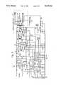
- FIG. 1is a schematic diagram of a boost converter in a first embodiment of the present invention that uses a center-tapped output transformer;
- FIG. 2is a schematic diagram of a lighting system in a second embodiment of the present invention that uses two transistors in a half-bridge;
- FIG. 3is a top elevational view of the printed circuit board assembly for the lighting system of FIG. 2;
- FIG. 4is a functional block diagram of an electronic ballast chip in a third embodiment of the present invention.
- FIG. 5is a functional block diagram of an alternative electronic ballast chip in a fourth embodiment of the present invention and is similar to that of FIG. 4;
- FIG. 6is a top elevational view of the package for the electronic ballast chip of FIG. 5.
- FIG. 1illustrates a boost converter 10, in an embodiment of the present invention, which comprises a full-wave bridge rectifier 12, a filter capacitor 14, a voltage divider 16 that produces a sample voltage "V ac " for power factor correction, a transformer 18 that similarly produces at its secondary a voltage, representing a current "i ac " that is proportional to the current through the primary of transformer 18 and is a sample used for power factor correction.
- a supply voltage "vcc”is provided by a diode 20, a filter capacitor 22, a dropping resistor 24 and a diode 25. Resistor 24 is chosen to limit the current supplied through diode 25.
- a power factor correction MOSFET 28is used to periodically short the output of the primary winding of transformer 18 to circuit common. The period of such a short must be necessarily limited in duration to achieve the desired active power factor correction inductive boost in the primary of transformer 18 and not destroy the transformer and/or MOSFET.
- a sample of voltage +Vs, labeled "Vdc"is produced by a voltage divider 30 and is the third component input used for power factor correction.
- a timing resistor (R t1 ) 32 and a timing capacitor (C t1 ) 34set the basic start-up delay, or filament warm-up time.
- a gain compensation capacitor 36, a gain compensation resistor 38 and an input resistor 40setup the gain characteristics of an op-amp that monitors current through the lamp load.
- a simple dropping resistor(not shown) may be used in series with the lamp load in a conventional way to sample lamp current.
- a base clock frequency of an oscillatoris determined by a resistor (R t2 ) 42 and a capacitor (C t2 ) 44.
- the frequency chosenis such that the network will be stimulated with pulses of voltage +Vs at a frequency for which the network produces voltages great enough to operate the lamps in the load.
- the frequency at which MOSFET 28 operatesis determined by the base clock frequency and the pulse duration at the gate is modulated to effectuate active power factor correction.
- a pair of resistors 46 and 48divide down sample current i ac for a ballast chip 50. Sample voltage V ac and i ac are multiplied together in chip 50 and compared to sample voltage V dc . The result is the degree of power factor correction required.
- a pair of MOSFET transistors 52 and 54are driven at their respective gates by chip 50 such that an alternating current is produced in the primary of a transformer 56.
- a winding 58supplies filament voltage to the load lamps.
- Transformer 56is typically driven by chip 50 via MOSFETs 52 and 54 at a first frequency that produces a filament current in winding 58 and then at a second frequency that operates with transformer 56 and the network and load to produce ionizing voltages in the load lamps.
- Chip 50regulates the current through the load lamps by adjusting the frequency and/or duty cycle of the gate drive signals applied to MOSFETs 52 and 54.
- Resistor 32 and capacitor 34set a filament heating time period in chip 50 that adjusts the delay time before high voltage is applied across the lamps. This delay helps ensure the life of lamps.
- Resistor 42 and capacitor 44set a resistor-capacitor (RC) time constant for an oscillator within chip 50 that determines the base frequency of operation.
- RCresistor-capacitor
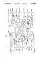
- FIG. 2illustrates a system 100 that includes a configurable output section 102.
- An output transformer 104has four secondary windings and is part of a network that can be adapted to suit a variety of lamp types and configurations.
- An electronic ballast chip 106is similar to ballast chip 50, and much of the functional operation within system 100 is therefore the same. The pinout of ballast chip 106 is described in more detail by Table I.
- a transformer 108is used to DC isolate ballast chip 106 from the gate of a high-side MOSFET 110 that must necessarily operate near a high voltage +Vs.
- a second MOSFET 112 and MOSFET 110are similar in function to MOSFETs 54 and 52 (FIG. 1). Transformer 104 does not have a center-tapped primary as does transformer 56 in FIG.
- transformer 104must be driven in a way that develops the AC currents from a single voltage +Vs.
- Current through the gaseous discharge lamp load(not shown, but attached to section 102) is sampled by a transformer 114.
- a voltage proportional to the lamp load currentis returned via a series of resistors 116 and 118, a diode 119 and a resistor 120 to ballast chip 106, and is referred to herein as "Isense".
- a current injected via a diode 122 and a resistor 124will modify the value of "I SENSE" and has the effect of a dimming control.
- the basic level of operatione.g.
- the level of lamp load currentis established by a voltage injected into transformer 114 by a voltage divider 126 connected to a voltage reference "Vref".
- a timer resistor 128 and a capacitor 130set the preheat and lamp-out-of-socket interrupt period for a timer within chip 106.
- a resistor 132 and a capacitor 134similarly setup the basic frequency period of an oscillator included in chip 106.
- a full-wave rectified input voltageis sampled by ballast chip 106 for power factor correction through a resistor 136. The input current is detected by dropping it across a resistor 138 and feeding the resultant voltage through a resistor 140 to ballast chip 106.
- the inputs necessary for power factor correctionare combined within ballast chip 106 and used to modulate a control signal applied to the gate of a boost MOSFET 142.
- the input current coupled through resistor 140is forced to follow the voltage coupled through resistor 136 by switching a boost inductor 144 periodically to circuit common through MOSFET 142.
- a diode 146allows surge bypass around boost inductor 144 to a series combination of a pair of capacitors 148 and 150.
- a diode 152isolates capacitors 148 and 150 from boost inductor 144 and prevents the charge on the capacitors from discharging through MOSFET 142.
- VAC120 volt alternating current
- the voltage across capacitors 148 and 150will be about 250 volts.
- a sample of this voltage, referred to as V dcis divided by a set of resistors 154, 156 and 158 and input to ballast chip 106 for the purpose of regulating Vdc.
- Table Ilists the pinouts and pin numbering of ballast chip 106.
- Chip 50has a different pin configuration. In FIG. 2, pin number "1" is identified on chip 106 and the numbering progresses counter-clockwise.
- the semi-standard tile array methodology of Micro Linear Corporation(San Jose, Calif.) has been used successfully and may be used to provide customized versions optimized to specific ballast architectures.
- a system using such a chipis capable of power factors better than 0.99 with low input current total harmonic distortion (THD) at better than 95% efficiency.
- TDDtotal harmonic distortion
- PCBA 200A printed circuit board assembly (PCBA) 200 is illustrated in FIG. 3 and represents one way that the components of system 100 may be arranged successfully. Other layouts are possible. Component locations are identified on PCBA 200 by using their element numbers of FIG. 2. The layout of FIG. 3 has been configured to demonstrate the versatility of chip 106 to potential users.
- FIG. 4illustrates a chip embodiment of the present invention, and is referred to by the general reference numeral 300, and is functionally similar to ballast chips 50 and 106.
- Chip 300may be fabricated with a conventional low voltage (10 V-20 V) bipolar process and has a die size that may be expected to be approximately one hundred mils square.
- a shunt regulator 302maintains a 13.5 volt level within chip 300 and is fed with an external current source at a pin labeled +Vcc. If a series regulator were used instead, it would dissipate substantially more power than does shunt regulator 302, and so it would be less efficient and contribute to the unnecessary heating of chip 300. Shunt regulation prevents a condition where twenty-five volts or more could appear on chip 300.
- An undervoltage lockout 304prevents chip 300 from operating during low line voltage situations, such as brown outs, and which are reflected in low levels of +Vcc. As gaseous discharge lamps in the output network driven by chip 300 starve for current, a short lamp life condition can develop. Undervoltage lockout 304 prevents such operation by effectively turning chip 300 off.
- undervoltage lockout 304has a hysteresis circuit that operates, for example, at ten and twelve volts.
- Chip 300further includes a voltage reference (Vref) 306 that may either be five volts or 7.5 volts or any other convenient voltage.
- Vrefvoltage reference
- Undervoltage lockout 304requires that Vref assume a proper level, otherwise it will disable chip 300.
- a timer bias control 308 and an “other" bias control 310supply internal current mirrors and other biasing that prevents operational drifts with changes in chip 300 temperature.
- a current reference generator 312supplies a set of constant current sources for an oscillator (“Io"), a timer (“It”) and an analog multiplier ("Im").
- timing resistors and capacitorsallow timing resistors and capacitors to both be tied from a pin on chip 300 to circuit common, rather than tying the resistor as a pull-up to +Vcc or Vref, as are resistors 32 and 42 in FIG. 1.
- a pin labeled “R REF”allows current reference generator 312 to be programmed with an external resistor to circuit common.
- a timer 314has an external resistor and capacitor (Rt and Ct) that set the time period that the lamp filaments in an output load are allowed to heat before the full voltage is applied across them. Lamp life will be improved if the warm-up, or start-up time is sufficiently extended, e.g., 0.6 to 0.7 seconds.
- chip 300can accommodate a filament warm-up time of zero by the simple elimination of capacitor Ct, or by a resistor of sufficient value in series with Ct.
- a high temperature shutdown 316senses heat that has soaked into chip 300 from the outside ambient air. Ballast operation will be suspended in the temperature sensed (the junction temperature) exceeds, for example, 100° or 120° Celsius (C).
- the die temperature of chip 300is as follows in equation (1): ##EQU1## Heat sources on chip 300 itself are normally relatively insignificant and have no substantial masking effect on the operation of high temperature shutdown 316. Instead, these sources act as an offset.
- the thermal resistance of chip 300 to its package and to the ambientis about normal for a twenty-pin plastic DIP giving a 20° C. junction temperature rise.
- High temperature shutdown 316is able to perform its job satisfactorily because a shutdown is required only after the ambient has exceeded a predetermined maximum for typically thirty minutes, which is more than enough time for the heat to soak into chip 300 and to equalize across the thermal resistance of the package and chip 300 junction.
- the actual temperature sensing element within shutdown 316may comprise a string of diodes in series in a conventional configuration.
- a "V be " amplifiermay also be used as a two terminal device to sense temperature. High temperature shutdown is effectuated by forcing the drive outputs of chip 300 off.
- the on-chip heat dissipation of chip 300which acts as an offset can be used to vary the thermal trip point of the high temperature shutdown 316. If more or less constant current is pumped into shunt regulator 302, the thermal trip point will be modulated accordingly.
- Timer 314sets the time period in which a lamp network that has been detected as being off is put through an attempt to restart, for example every two seconds.
- timer 314is a single dual-threshold type that uses a common resistor-capacitor set and different triggering thresholds to extract double duty operation.
- One time periodis used for start-up timing and the other for lamp-out-of-socket interrupt timing.
- An error op-amp 318amplifies a "LAMP I SENSE" signal derived from a lamp current sensing circuit in the output load.
- a closed-loop servois implemented thereby establishing a control point that stabilizes lamp current and brightness.
- a modification of the control-pointcan vary lamp brightness and thereby behave as a dimming control.
- a mode control 320steers the output of op-amp 318 according to the state of a signal on a "MODE" input.
- a variable oscillator 322operates at a variety of frequencies, depending on the values of an external resistor and capacitor combination and the constant current source "Io". In a frequency control mode, the constant current source "Io" is modified by op-amp 318 and steered to oscillator 322 such that its output frequency may be affected.
- a pulse width control modethe output of op-amp 318 is used to produce a reset signal that turns off a flip-flop, which has been turned on periodically by oscillator 322.
- one of a fixed frequency mode or a pulse width modemay be alternatively configured, and thereby eliminate the need for mode control 320.
- Oscillator 322outputs both a square wave signal and a saw-tooth signal.
- a typical operating frequency for oscillator 322is eighty kilohertz, which produces a frequency of forty kilohertz in the lamp load.
- the minimum lamp frequencyis preferably greater than twenty kilohertz, in order to keep it above the range of human hearing. Above 120 kilohertz, radio frequency emissions could become a problem and the rules of the Federal Communications Commission become a constraint.
- Oscillator 322does not "slow-start" by ramping between frequencies, as is common in the prior art.
- start-upwhich is also referred to as pre-heat
- timer 314signals oscillator 322 via mode control 320 to run at a frequency or pulse width that does not produce ionizing voltages in the output load but does develop filament current.
- a dimming control signalis accomplished with a current that is injected into the RC network.
- the exact frequency or pulse width necessary during start-upis a function of the output network and types of lamps used.
- a T-type flip-flop 324toggles at half the frequency of oscillator 322 and produces the complementary digital output signals for a pair of MOSFET gate drives labeled "OUT -- 3" and "OUT -- 2".
- a reset-set (RS) flip-flop 326enables both MOSFET gate drives to be controlled by the complementary outputs of flip-flop 324.
- the RS flip-flop 326terminates the output pulses to both MOSFET gate drives, effectively disabling them, when the sense current (LAMP I SENSE) from op-amp 318 exceeds a threshold labeled "Vref", which is derived from voltage reference 306.
- a set signalarrives at flip-flop 326 from oscillator 322 each period.
- a reset signalarrives later each period from op-amp 318 via mode control 320. The effect is a fixed frequency, pulse width modulated closed-loop servo control of lamp current.
- variable frequency mode and variable pulse width modeallows a ballast designer a great deal of flexibility in the choice of output networks and lamps that can be used with chip 300.
- the current necessary for MOSFET gate driveis provided by a pair of buffers 328 and 330.
- the logic necessary to translate the outputs of flip-flops 324 and 326 to MOSFET gate drives OUT -- 3 and OUT -- 2is provided by a pair of gates 332 and 334.
- a gate 336controls an output enable control on buffers 328 and 330, and can effectively turn off the output from chip 300 by inhibiting OUT -- 3 and OUT -- 2.
- Chip 300includes an active power factor correction feature that forces the input AC current to be sinusoidal.
- the theory and application of average current mode power factor correction controllersis described in detail by Mehmet K. Nalbant and William Cho in Application Note 16, "Theory and Application of the ML4821 Average Current Mode PFC Controller", published by Micro Linear Corporation (San Jose, Calif.), January 1992.
- Chip 300uses a PFC configuration similar to that shown in FIG. 2 of the Nalbant & Cho application note.
- An op-amp 338operates as an error amplifier in a voltage control loop and receives at its inverting input a sample of the voltage output by the boost converter. In FIG. 1 this point is at the top of divider 30.
- the inverting inputis connected to a pin labeled "VDC SENSE”.
- An analog multiplier 340receives the signal from op-amp 338 and a current at a pin labeled "I SINE” that is proportional to the voltage of a full-wave rectified sinewave.
- the control objectiveis to force the input current waveshape to follow the shape of the input voltage, and thereby correct the power factor to approach unity. It does this by modulating the duty cycle of a boost MOSFET driven at its gate by a pin labeled OUT -- 1.
- Multiplier 340has its output connected to a pin labeled "MULT OUT" and to the non-inverting input of an op-amp 342.
- a sample of the input current waveformis injected as a current into the non-inverting input of op-amp 342 via the MULT OUT pin.
- FIG. 2shows this being done with resistor 140.
- the current through the loadproduces a voltage drop across resistor 138 that is proportional to the input current.
- FIGS. 5 and 6illustrate an alternative embodiment of an electronic ballast chip, according to the present invention, and referred to by the general reference number 400.
- Ballast chip 400is similar to ballast chip 300 in several major respects. Some functions have been combined and others added. A few of the functional terms are different and reflect the range the individual functions can assume.
- Ballast chip 400comprises a preheat and interrupt timer 402, a voltage controlled current source 404, an undervoltage and thermal shutdown 406, a linear current input multiplier 408, a pair of RS flip-flops 410 and 412, a T-type flip-flop 414 and an oscillator 416.
- the timing for preheat, dimming lockout and interruptare set by a resistor-capacitor combination connected externally to the pin labeled "R(X)/C(X)", e.g., resistor 128 and capacitor 130 in FIG. 2.
- An external resistor connected between the pin labeled “R(SET)” and circuit commonfixes the maximum frequency Fmax of oscillator 416, the Iout of multiplier 408 and the charging current directed to R(X)/C(X).
- the output of multiplier 408is a current which appears on the "IA+" pin to form the reference for a current error amplifier (EA) 418.
- EAcurrent error amplifier
- the multiplier 408 output currentis converted into the reference voltage for a current amplifier (IA) 420 through a resistor to circuit common.
- a pin labeled "MODE”sets the operating mode of chip 400 according to the logic shown in Table II.
- the lamp feedbackcontrols the two voltage controlled oscillator (VCO) ranges.
- VCOvoltage controlled oscillator
- the charging current to C(T)decreases, thereby causing oscillator 416 to decrease in frequency.
- the ballast output networkacts as a high pass filter, the power to the lamps will be increased.
- a larger C(T) value and a lower R(T) valuecan be used, to yield a smaller (narrower) frequency excursion over the control range of the LFB OUT pin.
- the discharge currentis set to five milliamps in VCO mode and thirty-five milliamps in the VC07 mode.
- the error amplifier 418serves the same purpose as op-amp 338 and its associated pinouts are labeled "EA” rather than Vdc.
- the current sense amplifier (IA) 420serves the same purpose as op-amp 342 and its associated pinouts are labeled "IA” rather than +I SENSE.
- Shutdown 406combines both undervoltage and thermal protection and an inhibit signal is sent to a three-input OR-gate 421. Hysteresis is provided in both the undervoltage and thermal sensing to eliminate chattering of the inhibit signal that would otherwise result. Other input signals are received from timer 402 and over voltage and inhibit input (OVP/INHIBIT).
- the PFC OUT pinWhen the voltage of the OVP/INHIBIT pin exceeds five volts, the PFC OUT pin is inhibited. When the voltage of the OvP/INHIBIT pin exceeds 6.8 volts, the PFC OUT, OUTA and OUTB output pins are inhibited, effectively turning chip 400 off. Power factor correction is communicated out of chip 400 by a three-input NOR-gate 422 and a buffer 424 to an output pin labeled "PFC OUT". This output is equivalent to OUT -- 1 in FIG. 4. A means must be provided to prevent a 100% on duty cycle from appearing at PFC OUT, otherwise the boost MOSFET and/or boost inductor can be destroyed.
- oscillator 416can be configuring oscillator 416 to never have a perfectly square output waveform (50% duty cycle). Another way is to provide a delay around flip-flop 412 that disables PFC OUT for some minimal time each clock period of oscillator 416.
- a pair of four-input NOR-gates 426 and 428translate ballast MOSFET gate control signals from flip-flops 412 and 414 out through a pair of buffers 430 and 432 to output pins labeled "OUTA" and "OUTB".
- Chip 400could be used in the system of FIG. 2 to replace ballast chip 106.
- Lamp feedback (LFB)is used to adjust current source 404 and therefore the behavior of oscillator 416.
- Pins labeled "LFB OUT" and "LAMP FB"are equivalent to pins labeled "Error Amp Out” and "Lamp I Sense” in FIG. 4.
- the lamp starting scenario of chip 400is preferably designed to maximize lamp life and minimize ballast heating during lamp out conditions.
- Timer 402controls the lamp starting scenarios of filament preheat and lamp-out-of-socket (lamp out) interrupt.
- Capacitor C(X)is charged with a current set by source 404 and discharged through R(X).
- the voltage at C(X)is initialized to 0.7 volts (one Vbe) at power up.
- the time for C(X) to rise to 3.4 voltsis the filament preheat time.
- the oscillator charging currentwill produce a high frequency (or low duty cycle) for filament pre-heat, but will not produce sufficient voltage to ignite the lamp.
- Gate drive outputs OUTA and OUTBare affected accordingly.
- the inverter frequency or pulse widthchanges to a point that causes a high voltage to appear that will ignite (ionize) the lamp. If the voltage does not drop at a time when the lamp is supposed to have ignited, the lamp feedback voltage coming into the "LAMP FB" pin will rise above Vref.
- the C(X) charging currentis shut off and the inverter is inhibited until C(X) is discharged by R(X) to a 1.2 volt threshold. By shutting off in this way, excessive heat generation is prevented when a lamp fails to strike or is out of socket.
- Function-reduced versions with fewer pinsare also desirable in certain cost-sensitive and space-sensitive applications.
- ballast chip 400is the industry standard twenty-pin dual inline plastic package (DIP) with 0.3 inch spacing between pin rows, such as is shown in FIG. 6.
- DIPdual inline plastic package
- the plastic, or molded DIPis also suitable for ballast chips 50, 106 and 300.
Landscapes
- Engineering & Computer Science (AREA)
- Power Engineering (AREA)
- Circuit Arrangements For Discharge Lamps (AREA)
- Dc-Dc Converters (AREA)
- Rectifiers (AREA)
- Discharge-Lamp Control Circuits And Pulse- Feed Circuits (AREA)
Abstract
Description
TABLE I ______________________________________ pin pin no. symbol function ______________________________________ 1 IA- Inverting input of the power factor correction average current error amplifier. 2 IA OUT Output and compensation node of the power factor correction average current error amplifier. 3 I(SINE) Power factor correction current multiplier input. 4 IA+ Non-inverting input of the power factor correction average current error amplifier. A negative current sense signal may be used onPin 4 in place of a positive input onpin 1. 5 LAMP FB Inverting input of lamp arc current error amplifier and input node for dimmer control. Dimming is accomplished by summing additional current to this pin. 6 LAMP FB Output of lamp current error OUT amplifier and lamp current loop compensation. 7 R(SET) Oscillator Fmax, multiplier max Iout, and Cx charging current set by an external resistor to circuit common. 8 MODE Controls lamp current error amp and preheat timers and choice amongst two variable frequency and one pulse width modulation mode. Connecting this pin to circuit common allows variable frequency control. Leavingpin 8 open increases the oscillator discharge current to 35.0 mA. ConnectingPin 8 to Vref allows variable underlapping pulse width control. Dead time between output pulses is provided in both modes. 9 Rt, Ct Oscillator timing components. The oscillator frequency is insensitive to temperature, chip to chip variations, etc., and determined only from the values of Ct and Rt. Desirable range of values are 360 picofarads to ten nanofarads for Ct and 4.7K ohms to 100K ohms for Rt. During the initial VCO mode start period (0.7 seconds) an oscillator current source of 96 microamperes is connected to pin 9, at the end of this period a current source of zero to 192 microamperes is activated. 10 INTERRUPT A voltage greater than Vref resets the chip and causes a restart after a delay of three times the start interval (used for lamp-out detection and restart). 11 OVP/ The power factor correction output INHIBIT is inhibited when this pin exceeds five volts; the chip function is inhibited and is reset when this pin exceeds 6.8 volts. 12 Rx/Cx A capacitor connected to this pin sets the basic timing for the preheat, dimming lockout and interrupt functions. A capacitor to circuit common from this pin provides a delay period at turn-on to lockoutcertain chip 300 functions that can interfere with proper lamp starting. The delay period is nominally two seconds. After starting and lamp out detection, Rx sets the interval between restart attempts. 13 GND Chip circuit common. 14 OUT B Ballast MOSFET drive output.14 and 15 are opposite phase outputs for the gate drives of the two output inverter power MOSFETs. 15 OUT A These outputs preferably should not cause latching or Pins chip 300 malfunction if the pin is driven above Vcc or below circuit common. The frequency of the gate drives is one half that of the master oscillator. 16 PFC OUT This is the gate drive output for the active power factor boost converter power MOSFET. This output preferably should not cause latching orchip 300 malfunction if the pin is driven above Vcc or below circuit common. The frequency of the gate drive is the same as that of the master oscillator. 17 +Vcc Vcc positive power supply for the chip. This pin has an internal shunt regulator to circuit common, with a nominal value of 13.5 volts ± 5%. Associated with the shunt regulator is the Vref circuit, under-voltage lockout, start-up hysteresis andchip 300 bias circuitry.Chip 300 should draw minimal current until after the voltage onpin 17 rises above the start-up voltage, which is 0.5 to one volt less than the shunt regulating value. 18 Vref Buffered output to provide a stable voltage reference derived from an internal bandgap reference. 19 EA- Inverting input to the power factor correction error amplifier for sensing and regulating the boost converter output DC voltage. The non-inverting input is internally connected to Vref. 20 EA OUT Power factor correction error amplifier output and compensation node. ______________________________________
TABLE II ______________________________________ Operational MODE MODE Input Pin Definition ______________________________________ VCO circuit wide range FM common VCO7 open narrow range FM PWM Vref pulse width modulation ______________________________________
Claims (16)
Priority Applications (7)
| Application Number | Priority Date | Filing Date | Title |
|---|---|---|---|
| US07/896,152US5315214A (en) | 1992-06-10 | 1992-06-10 | Dimmable high power factor high-efficiency electronic ballast controller integrated circuit with automatic ambient over-temperature shutdown |
| KR1019940700393AKR970011552B1 (en) | 1992-06-10 | 1993-06-09 | Dimmable, high power factor, high efficiency electronic ballast controller with automatic high temperature stop circuit |
| CA002114852ACA2114852C (en) | 1992-06-10 | 1993-06-09 | Dimmable high power factor high-efficiency electronic ballast controller integrated circuit with automatic ambient over-temperature shutdown |
| PCT/US1993/005581WO1993025952A1 (en) | 1992-06-10 | 1993-06-09 | Dimmable high power factor high-efficiency electronic ballast controller integrated circuit with automatic ambient over-temperature shutdown |
| EP93915296AEP0598110A4 (en) | 1992-06-10 | 1993-06-09 | Dimmable high power factor high-efficiency electronic ballast controller integrated circuit with automatic ambient over-temperature shutdown. |
| JP6501732AJPH06508475A (en) | 1992-06-10 | 1993-06-09 | Dimmable high power factor high frequency electronic ballast control integrated circuit with automatic shutoff function when a predetermined limit outside temperature is reached |
| FI940601AFI940601A7 (en) | 1992-06-10 | 1994-02-09 | High power factor and efficiency dimmable electronic ballast integrated circuit with automatic ambient overtemperature cut-off |
Applications Claiming Priority (1)
| Application Number | Priority Date | Filing Date | Title |
|---|---|---|---|
| US07/896,152US5315214A (en) | 1992-06-10 | 1992-06-10 | Dimmable high power factor high-efficiency electronic ballast controller integrated circuit with automatic ambient over-temperature shutdown |
Publications (1)
| Publication Number | Publication Date |
|---|---|
| US5315214Atrue US5315214A (en) | 1994-05-24 |
Family
ID=25405713
Family Applications (1)
| Application Number | Title | Priority Date | Filing Date |
|---|---|---|---|
| US07/896,152Expired - Fee RelatedUS5315214A (en) | 1992-06-10 | 1992-06-10 | Dimmable high power factor high-efficiency electronic ballast controller integrated circuit with automatic ambient over-temperature shutdown |
Country Status (7)
| Country | Link |
|---|---|
| US (1) | US5315214A (en) |
| EP (1) | EP0598110A4 (en) |
| JP (1) | JPH06508475A (en) |
| KR (1) | KR970011552B1 (en) |
| CA (1) | CA2114852C (en) |
| FI (1) | FI940601A7 (en) |
| WO (1) | WO1993025952A1 (en) |
Cited By (74)
| Publication number | Priority date | Publication date | Assignee | Title |
|---|---|---|---|---|
| US5387847A (en)* | 1994-03-04 | 1995-02-07 | International Rectifier Corporation | Passive power factor ballast circuit for the gas discharge lamps |
| US5396155A (en)* | 1994-06-28 | 1995-03-07 | Energy Savings, Inc. | Self-dimming electronic ballast |
| US5502838A (en)* | 1994-04-28 | 1996-03-26 | Consilium Overseas Limited | Temperature management for integrated circuits |
| US5539281A (en)* | 1994-06-28 | 1996-07-23 | Energy Savings, Inc. | Externally dimmable electronic ballast |
| EP0788298A1 (en)* | 1995-07-31 | 1997-08-06 | General Electric Company | Reduced bus-voltage integrated-boost high power-factor circuit for powering gas discharge lamps |
| US5668446A (en)* | 1995-01-17 | 1997-09-16 | Negawatt Technologies Inc. | Energy management control system for fluorescent lighting |
| US5705896A (en)* | 1995-03-30 | 1998-01-06 | Samsung Electronics Co., Ltd. | Control electronic ballast system using feedback |
| US5744912A (en)* | 1996-06-26 | 1998-04-28 | So; Gin Pang | Electronic ballast having an oscillator shutdown circuit for single or multiple fluorescent tubes for lamps |
| US5757630A (en)* | 1995-09-05 | 1998-05-26 | Electronic Lighting, Inc. | Control circuit with improved functionality for non-linear and negative resistance loads |
| US5770926A (en)* | 1995-12-28 | 1998-06-23 | Samsung Electronics, Co., Ltd. | Feedback control system of an electronic ballast which detects arcing of a lamp |
| US5806055A (en)* | 1996-12-19 | 1998-09-08 | Zinda, Jr.; Kenneth L. | Solid state ballast system for metal halide lighting using fuzzy logic control |
| US5818709A (en)* | 1994-11-15 | 1998-10-06 | Minebea Co., Ltd. | Inverter apparatus |
| US5821700A (en)* | 1996-12-20 | 1998-10-13 | Star Headlight & Lantern Co. | Visual warning system for a railway vehicle |
| US5834903A (en)* | 1993-10-28 | 1998-11-10 | Marshall Electric Corporation | Double resonant driver ballast for gas lamps |
| WO1999014990A1 (en)* | 1997-09-18 | 1999-03-25 | Everbrite, Inc. | Floating driver having common emitter drive stage |
| US5949196A (en)* | 1997-03-13 | 1999-09-07 | Lumatech Corporation | Method and system for switchable light levels in operating gas discharge lamps with an inexpensive single ballast |
| US5952832A (en)* | 1996-12-06 | 1999-09-14 | General Electric Company | Diagnostic circuit and method for predicting fluorescent lamp failure by monitoring filament currents |
| US5960207A (en)* | 1997-01-21 | 1999-09-28 | Dell Usa, L.P. | System and method for reducing power losses by gating an active power factor conversion process |
| US6043612A (en)* | 1997-04-12 | 2000-03-28 | Vossloh-Schwabe Gmbh | Electronic ballast with automatic restarting |
| US6051933A (en)* | 1995-04-28 | 2000-04-18 | Sgs-Thomson Microelectronics S.R.L. | Bipolar power device having an integrated thermal protection for driving electric loads |
| WO2000040058A1 (en)* | 1998-12-29 | 2000-07-06 | Koninklijke Philips Electronics N.V. | Dimmable electronic ballast with single stage feedback inverter |
| US6107755A (en)* | 1998-04-27 | 2000-08-22 | Jrs Technology, Inc. | Modular, configurable dimming ballast for a gas-discharge lamp |
| US6172466B1 (en) | 1999-02-12 | 2001-01-09 | The Hong Kong University Of Science And Technology | Phase-controlled dimmable ballast |
| US6175198B1 (en) | 1999-05-25 | 2001-01-16 | General Electric Company | Electrodeless fluorescent lamp dimming system |
| US6181086B1 (en) | 1998-04-27 | 2001-01-30 | Jrs Technology Inc. | Electronic ballast with embedded network micro-controller |
| AT407461B (en)* | 1996-04-24 | 2001-03-26 | Kurz Martin | CONTROL FOR DISCHARGE LAMP |
| US6211623B1 (en)* | 1998-01-05 | 2001-04-03 | International Rectifier Corporation | Fully integrated ballast IC |
| US6215255B1 (en)* | 1999-04-30 | 2001-04-10 | Fairchild Korea Semiconductor Ltd. | Electric ballast system |
| US6218788B1 (en) | 1999-08-20 | 2001-04-17 | General Electric Company | Floating IC driven dimming ballast |
| US6232727B1 (en) | 1998-10-07 | 2001-05-15 | Micro Linear Corporation | Controlling gas discharge lamp intensity with power regulation and end of life protection |
| WO2002021671A1 (en)* | 2000-09-05 | 2002-03-14 | Minebea Co. Ltd. | Active power factor correction |
| US6366032B1 (en) | 2000-01-28 | 2002-04-02 | Robertson Worldwide, Inc. | Fluorescent lamp ballast with integrated circuit |
| US6555971B1 (en)* | 2000-06-13 | 2003-04-29 | Lighttech Group, Inc. | High frequency, high efficiency quick restart lighting system |
| US6577066B1 (en)* | 1999-03-30 | 2003-06-10 | Matsushita Electric Industrial Co., Ltd. | Compact self-ballasted fluorescent lamp |
| SG96563A1 (en)* | 2000-06-12 | 2003-06-16 | Matsushita Electric Works Ltd | Electronic ballast for a discharge lamp |
| US6617805B2 (en)* | 2000-10-20 | 2003-09-09 | International Rectifier Corporation | Ballast control IC with power factor correction |
| US6621239B1 (en) | 2000-03-14 | 2003-09-16 | Richard S. Belliveau | Method and apparatus for controlling the temperature of a multi-parameter light |
| US20040012347A1 (en)* | 2002-07-22 | 2004-01-22 | International Rectifier Corporation | Single chip ballast control with power factor correction |
| WO2003101151A3 (en)* | 2002-05-28 | 2004-04-22 | Matsushita Electric Works Ltd | Electronic ballast for a discharge lamp |
| US6762569B1 (en) | 2003-01-10 | 2004-07-13 | Henkel Corporation | Constant light output circuit and electrical components based thereon |
| US20040232852A1 (en)* | 2003-05-22 | 2004-11-25 | Patent-Treuhand-Gesellschaft Fur Elektrisch Gluhlampen Mbh | Method for operation of a lighting system |
| WO2005013647A1 (en)* | 2003-08-05 | 2005-02-10 | Koninklijke Philips Electronics, N.V. | Total harmonic distortion reduction for electronic dimming ballast |
| US6856100B1 (en)* | 2003-09-30 | 2005-02-15 | Osrom Sylvania, Inc. | Ballast with inverter startup circuit |
| US20050088112A1 (en)* | 2003-09-08 | 2005-04-28 | S K America, Inc. | Fluorescent lamp dimmer control |
| WO2005046038A1 (en) | 2003-11-10 | 2005-05-19 | The University Of Hong Kong | Dimmable ballast with resistive input and low electromagnetic interference |
| US20060255751A1 (en)* | 2003-11-12 | 2006-11-16 | Lutron Electronics Co., Inc. | Thermal protection for lamp ballasts |
| US20070108915A1 (en)* | 2005-03-15 | 2007-05-17 | Ribarich Thomas J | 8-Pin PFC and ballast control IC |
| US7235933B1 (en)* | 2006-02-27 | 2007-06-26 | Yu-Sheng So | Reversible dimmer device of gas discharge lamps and the control method for light adjusting thereof |
| US20080315797A1 (en)* | 2007-03-05 | 2008-12-25 | Ceyx Technologies, Inc. | Method and firmware for controlling an inverter voltage by drive signal frequency |
| US20090090117A1 (en)* | 2007-10-08 | 2009-04-09 | Emerson Climate Technologies, Inc. | System and method for monitoring overheat of a compressor |
| US20090090118A1 (en)* | 2007-10-08 | 2009-04-09 | Emerson Climate Technologies, Inc. | Variable speed compressor protection system and method |
| US20090094997A1 (en)* | 2007-10-08 | 2009-04-16 | Emerson Climate Technologies, Inc. | System and method for calibrating parameters for a refrigeration system with a variable speed compressor |
| US20090230882A1 (en)* | 2008-03-11 | 2009-09-17 | Hendrik Santo | Architecture and technique for inter-chip communication |
| US20090231247A1 (en)* | 2008-03-11 | 2009-09-17 | Tushar Dhayagude | Methods and circuits for self-calibrating controller |
| US20090241592A1 (en)* | 2007-10-05 | 2009-10-01 | Emerson Climate Technologies, Inc. | Compressor assembly having electronics cooling system and method |
| CN100549804C (en)* | 2006-08-09 | 2009-10-14 | 明基电通股份有限公司 | Power factor correction circuit and associated projector |
| US20090267652A1 (en)* | 2008-04-28 | 2009-10-29 | Hendrik Santo | Methods and circuits for triode region detection |
| US20090302772A1 (en)* | 2008-06-09 | 2009-12-10 | Technical Consumer Products, Inc. | Fluorescent lamp dimming circuit |
| US20090315467A1 (en)* | 2008-06-24 | 2009-12-24 | Msilica Inc | Apparatus and methodology for enhancing efficiency of a power distribution system having power factor correction capability by using a self-calibrating controller |
| US20100237786A1 (en)* | 2009-03-23 | 2010-09-23 | Msilica Inc | Method and apparatus for an intelligent light emitting diode driver having power factor correction capability |
| CN101009967B (en)* | 2006-01-24 | 2010-09-29 | 鸿富锦精密工业(深圳)有限公司 | Dimming mode selection circuit and discharge lamp driving device using the same |
| CN101291106B (en)* | 2007-04-20 | 2010-12-01 | 台达电子工业股份有限公司 | Sampling method to adjust duty cycle |
| US20110129354A1 (en)* | 2007-10-05 | 2011-06-02 | Emerson Climate Technologies, Inc. | Vibration Protection In A Variable Speed Compressor |
| US20110187271A1 (en)* | 2010-02-01 | 2011-08-04 | Twisthink, L.L.C. | Luminary control systems |
| WO2012059853A1 (en)* | 2010-11-03 | 2012-05-10 | Koninklijke Philips Electronics N.V. | Driver device and driving method for driving a load, in particular an led unit |
| US8418483B2 (en) | 2007-10-08 | 2013-04-16 | Emerson Climate Technologies, Inc. | System and method for calculating parameters for a refrigeration system with a variable speed compressor |
| US8448459B2 (en) | 2007-10-08 | 2013-05-28 | Emerson Climate Technologies, Inc. | System and method for evaluating parameters for a refrigeration system with a variable speed compressor |
| US8860313B2 (en) | 2011-11-30 | 2014-10-14 | Lutron Electronics Co., Inc. | Universal-voltage self-heating thermal detector |
| US8950206B2 (en) | 2007-10-05 | 2015-02-10 | Emerson Climate Technologies, Inc. | Compressor assembly having electronics cooling system and method |
| AT516394B1 (en)* | 2007-06-22 | 2016-05-15 | Tridonic Gmbh & Co Kg | ELECTRONIC BALLAST WITH PFC |
| EP2130407B1 (en)* | 2007-03-12 | 2017-08-30 | Philips Lighting Holding B.V. | Power control system for current regulated light sources |
| AT15719U1 (en)* | 2017-02-23 | 2018-04-15 | Tridonic Gmbh & Co Kg | PFC circuit |
| AT16509U1 (en)* | 2014-10-14 | 2019-11-15 | Tridonic Gmbh & Co Kg | Sensor for a control gear for bulbs |
| US11206743B2 (en) | 2019-07-25 | 2021-12-21 | Emerson Climate Technolgies, Inc. | Electronics enclosure with heat-transfer element |
Families Citing this family (6)
| Publication number | Priority date | Publication date | Assignee | Title |
|---|---|---|---|---|
| US5545955A (en)* | 1994-03-04 | 1996-08-13 | International Rectifier Corporation | MOS gate driver for ballast circuits |
| JPH08115797A (en)* | 1994-10-07 | 1996-05-07 | Samsung Electron Co Ltd | Automatic dimming device for discharge lamp |
| SG68587A1 (en)* | 1996-07-27 | 1999-11-16 | Singapore Productivity And Sta | An electronic ballast circuit |
| US6331755B1 (en) | 1998-01-13 | 2001-12-18 | International Rectifier Corporation | Circuit for detecting near or below resonance operation of a fluorescent lamp driven by half-bridge circuit |
| DE69919138T2 (en) | 1998-02-13 | 2005-08-18 | Lutron Electronics Co., Inc. | ELECTRONIC DIMMER |
| US7414372B2 (en) | 2005-10-24 | 2008-08-19 | International Rectifier Corporation | Dimming ballast control circuit |
Citations (5)
| Publication number | Priority date | Publication date | Assignee | Title |
|---|---|---|---|---|
| US4384213A (en)* | 1976-07-19 | 1983-05-17 | Westinghouse Electric Corp. | Automatic transfer control device |
| US4415839A (en)* | 1981-11-23 | 1983-11-15 | Lesea Ronald A | Electronic ballast for gaseous discharge lamps |
| US4629967A (en)* | 1985-04-29 | 1986-12-16 | General Motors Corporation | Generator voltage regulator |
| US4988889A (en)* | 1989-07-03 | 1991-01-29 | Self-Powered Lighting, Inc. | Power source for emergency lighting systems |
| US5204587A (en)* | 1991-02-19 | 1993-04-20 | Magnetek, Inc. | Fluorescent lamp power control |
Family Cites Families (6)
| Publication number | Priority date | Publication date | Assignee | Title |
|---|---|---|---|---|
| DE3266600D1 (en)* | 1981-02-21 | 1985-11-07 | Emi Plc Thorn | Lamp driver circuits |
| US4866350A (en)* | 1988-04-04 | 1989-09-12 | Usi Lighting, Inc. | Fluorescent lamp system |
| ATE103458T1 (en)* | 1988-04-20 | 1994-04-15 | Zumtobel Ag | BALLAST FOR A DISCHARGE LAMP. |
| FI100759B (en)* | 1989-12-29 | 1998-02-13 | Zumtobel Ag | Method and ballast device for attenuating fluorescent lamps |
| US5051662A (en)* | 1990-03-27 | 1991-09-24 | Usi Lighting, Inc. | Fluorescent lamp system |
| NL9002681A (en)* | 1990-12-05 | 1992-07-01 | Nedap Nv | BALLAST FOR FLUORESCENT LAMPS. |
- 1992
- 1992-06-10USUS07/896,152patent/US5315214A/ennot_activeExpired - Fee Related
- 1993
- 1993-06-09KRKR1019940700393Apatent/KR970011552B1/ennot_activeExpired - Fee Related
- 1993-06-09JPJP6501732Apatent/JPH06508475A/enactivePending
- 1993-06-09EPEP93915296Apatent/EP0598110A4/ennot_activeWithdrawn
- 1993-06-09WOPCT/US1993/005581patent/WO1993025952A1/ennot_activeApplication Discontinuation
- 1993-06-09CACA002114852Apatent/CA2114852C/ennot_activeExpired - Fee Related
- 1994
- 1994-02-09FIFI940601Apatent/FI940601A7/ennot_activeApplication Discontinuation
Patent Citations (5)
| Publication number | Priority date | Publication date | Assignee | Title |
|---|---|---|---|---|
| US4384213A (en)* | 1976-07-19 | 1983-05-17 | Westinghouse Electric Corp. | Automatic transfer control device |
| US4415839A (en)* | 1981-11-23 | 1983-11-15 | Lesea Ronald A | Electronic ballast for gaseous discharge lamps |
| US4629967A (en)* | 1985-04-29 | 1986-12-16 | General Motors Corporation | Generator voltage regulator |
| US4988889A (en)* | 1989-07-03 | 1991-01-29 | Self-Powered Lighting, Inc. | Power source for emergency lighting systems |
| US5204587A (en)* | 1991-02-19 | 1993-04-20 | Magnetek, Inc. | Fluorescent lamp power control |
Cited By (115)
| Publication number | Priority date | Publication date | Assignee | Title |
|---|---|---|---|---|
| US5834903A (en)* | 1993-10-28 | 1998-11-10 | Marshall Electric Corporation | Double resonant driver ballast for gas lamps |
| US5387847A (en)* | 1994-03-04 | 1995-02-07 | International Rectifier Corporation | Passive power factor ballast circuit for the gas discharge lamps |
| US5502838A (en)* | 1994-04-28 | 1996-03-26 | Consilium Overseas Limited | Temperature management for integrated circuits |
| US5396155A (en)* | 1994-06-28 | 1995-03-07 | Energy Savings, Inc. | Self-dimming electronic ballast |
| US5539281A (en)* | 1994-06-28 | 1996-07-23 | Energy Savings, Inc. | Externally dimmable electronic ballast |
| US5818709A (en)* | 1994-11-15 | 1998-10-06 | Minebea Co., Ltd. | Inverter apparatus |
| US5962989A (en)* | 1995-01-17 | 1999-10-05 | Negawatt Technologies Inc. | Energy management control system |
| US5668446A (en)* | 1995-01-17 | 1997-09-16 | Negawatt Technologies Inc. | Energy management control system for fluorescent lighting |
| US5705896A (en)* | 1995-03-30 | 1998-01-06 | Samsung Electronics Co., Ltd. | Control electronic ballast system using feedback |
| US6051933A (en)* | 1995-04-28 | 2000-04-18 | Sgs-Thomson Microelectronics S.R.L. | Bipolar power device having an integrated thermal protection for driving electric loads |
| EP0788298A1 (en)* | 1995-07-31 | 1997-08-06 | General Electric Company | Reduced bus-voltage integrated-boost high power-factor circuit for powering gas discharge lamps |
| US5757630A (en)* | 1995-09-05 | 1998-05-26 | Electronic Lighting, Inc. | Control circuit with improved functionality for non-linear and negative resistance loads |
| US5770926A (en)* | 1995-12-28 | 1998-06-23 | Samsung Electronics, Co., Ltd. | Feedback control system of an electronic ballast which detects arcing of a lamp |
| AT407461B (en)* | 1996-04-24 | 2001-03-26 | Kurz Martin | CONTROL FOR DISCHARGE LAMP |
| US5744912A (en)* | 1996-06-26 | 1998-04-28 | So; Gin Pang | Electronic ballast having an oscillator shutdown circuit for single or multiple fluorescent tubes for lamps |
| US5952832A (en)* | 1996-12-06 | 1999-09-14 | General Electric Company | Diagnostic circuit and method for predicting fluorescent lamp failure by monitoring filament currents |
| US5806055A (en)* | 1996-12-19 | 1998-09-08 | Zinda, Jr.; Kenneth L. | Solid state ballast system for metal halide lighting using fuzzy logic control |
| US5821700A (en)* | 1996-12-20 | 1998-10-13 | Star Headlight & Lantern Co. | Visual warning system for a railway vehicle |
| US5960207A (en)* | 1997-01-21 | 1999-09-28 | Dell Usa, L.P. | System and method for reducing power losses by gating an active power factor conversion process |
| US5949196A (en)* | 1997-03-13 | 1999-09-07 | Lumatech Corporation | Method and system for switchable light levels in operating gas discharge lamps with an inexpensive single ballast |
| US6043612A (en)* | 1997-04-12 | 2000-03-28 | Vossloh-Schwabe Gmbh | Electronic ballast with automatic restarting |
| WO1999014990A1 (en)* | 1997-09-18 | 1999-03-25 | Everbrite, Inc. | Floating driver having common emitter drive stage |
| US6211623B1 (en)* | 1998-01-05 | 2001-04-03 | International Rectifier Corporation | Fully integrated ballast IC |
| US6107755A (en)* | 1998-04-27 | 2000-08-22 | Jrs Technology, Inc. | Modular, configurable dimming ballast for a gas-discharge lamp |
| US6181086B1 (en) | 1998-04-27 | 2001-01-30 | Jrs Technology Inc. | Electronic ballast with embedded network micro-controller |
| US6232727B1 (en) | 1998-10-07 | 2001-05-15 | Micro Linear Corporation | Controlling gas discharge lamp intensity with power regulation and end of life protection |
| WO2000040058A1 (en)* | 1998-12-29 | 2000-07-06 | Koninklijke Philips Electronics N.V. | Dimmable electronic ballast with single stage feedback inverter |
| US6172466B1 (en) | 1999-02-12 | 2001-01-09 | The Hong Kong University Of Science And Technology | Phase-controlled dimmable ballast |
| US6577066B1 (en)* | 1999-03-30 | 2003-06-10 | Matsushita Electric Industrial Co., Ltd. | Compact self-ballasted fluorescent lamp |
| US6215255B1 (en)* | 1999-04-30 | 2001-04-10 | Fairchild Korea Semiconductor Ltd. | Electric ballast system |
| US6175198B1 (en) | 1999-05-25 | 2001-01-16 | General Electric Company | Electrodeless fluorescent lamp dimming system |
| US6218788B1 (en) | 1999-08-20 | 2001-04-17 | General Electric Company | Floating IC driven dimming ballast |
| US6366032B1 (en) | 2000-01-28 | 2002-04-02 | Robertson Worldwide, Inc. | Fluorescent lamp ballast with integrated circuit |
| US6621239B1 (en) | 2000-03-14 | 2003-09-16 | Richard S. Belliveau | Method and apparatus for controlling the temperature of a multi-parameter light |
| SG96563A1 (en)* | 2000-06-12 | 2003-06-16 | Matsushita Electric Works Ltd | Electronic ballast for a discharge lamp |
| US20040222752A1 (en)* | 2000-06-12 | 2004-11-11 | Yukio Yamanaka | Electronic ballast for a discharge lamp |
| US6943502B2 (en) | 2000-06-12 | 2005-09-13 | Matsushita Electric Works, Ltd. | Electronic ballast for a discharge lamp |
| US6555971B1 (en)* | 2000-06-13 | 2003-04-29 | Lighttech Group, Inc. | High frequency, high efficiency quick restart lighting system |
| WO2002021671A1 (en)* | 2000-09-05 | 2002-03-14 | Minebea Co. Ltd. | Active power factor correction |
| CN1452806B (en)* | 2000-09-05 | 2010-05-26 | 美蓓亚株式会社 | Active power factor correction device and method therefor |
| EP1327184A4 (en)* | 2000-10-20 | 2005-04-20 | Int Rectifier Corp | Ballast control ic with power factor correction |
| US6617805B2 (en)* | 2000-10-20 | 2003-09-09 | International Rectifier Corporation | Ballast control IC with power factor correction |
| CN100416440C (en)* | 2000-10-20 | 2008-09-03 | 国际整流器有限公司 | Ballast control with power factor correction |
| WO2003101151A3 (en)* | 2002-05-28 | 2004-04-22 | Matsushita Electric Works Ltd | Electronic ballast for a discharge lamp |
| US20040239262A1 (en)* | 2002-05-28 | 2004-12-02 | Shigeru Ido | Electronic ballast for a discharge lamp |
| US6954038B2 (en) | 2002-05-28 | 2005-10-11 | Matsushita Electric Works, Ltd. | Electronic ballast for a discharge lamp |
| US20040012347A1 (en)* | 2002-07-22 | 2004-01-22 | International Rectifier Corporation | Single chip ballast control with power factor correction |
| CN100392546C (en)* | 2002-07-22 | 2008-06-04 | 国际整流器公司 | Monolithic Ballast Control with Power Factor Correction |
| US6956336B2 (en)* | 2002-07-22 | 2005-10-18 | International Rectifier Corporation | Single chip ballast control with power factor correction |
| US6762569B1 (en) | 2003-01-10 | 2004-07-13 | Henkel Corporation | Constant light output circuit and electrical components based thereon |
| US20040232852A1 (en)* | 2003-05-22 | 2004-11-25 | Patent-Treuhand-Gesellschaft Fur Elektrisch Gluhlampen Mbh | Method for operation of a lighting system |
| US7075253B2 (en)* | 2003-05-22 | 2006-07-11 | Patent-Treuhand-Gesellschaft für elektrische Glühlampen mbH | Method for operation of a lighting system |
| WO2005013647A1 (en)* | 2003-08-05 | 2005-02-10 | Koninklijke Philips Electronics, N.V. | Total harmonic distortion reduction for electronic dimming ballast |
| US7279853B2 (en) | 2003-09-08 | 2007-10-09 | Maxlite - Sk America, Inc. | Fluorescent lamp dimmer control |
| US20050088112A1 (en)* | 2003-09-08 | 2005-04-28 | S K America, Inc. | Fluorescent lamp dimmer control |
| US6856100B1 (en)* | 2003-09-30 | 2005-02-15 | Osrom Sylvania, Inc. | Ballast with inverter startup circuit |
| WO2005046038A1 (en) | 2003-11-10 | 2005-05-19 | The University Of Hong Kong | Dimmable ballast with resistive input and low electromagnetic interference |
| US20060255751A1 (en)* | 2003-11-12 | 2006-11-16 | Lutron Electronics Co., Inc. | Thermal protection for lamp ballasts |
| US7675250B2 (en)* | 2003-11-12 | 2010-03-09 | Lutron Electronics Co., Inc. | Thermal protection for lamp ballasts |
| US7940015B2 (en) | 2003-11-12 | 2011-05-10 | Lutron Electronics Co., Inc. | Thermal protection for lamp ballasts |
| US20100171435A1 (en)* | 2003-11-12 | 2010-07-08 | Venkatesh Chitta | Thermal Protection For Lamp Ballasts |
| US20070108915A1 (en)* | 2005-03-15 | 2007-05-17 | Ribarich Thomas J | 8-Pin PFC and ballast control IC |
| US8164272B2 (en) | 2005-03-15 | 2012-04-24 | International Rectifier Corporation | 8-pin PFC and ballast control IC |
| KR100829239B1 (en)* | 2005-10-12 | 2008-05-14 | 인터내쇼널 렉티파이어 코포레이션 | 8-pin pfc and ballast control ic |
| CN101009967B (en)* | 2006-01-24 | 2010-09-29 | 鸿富锦精密工业(深圳)有限公司 | Dimming mode selection circuit and discharge lamp driving device using the same |
| US7235933B1 (en)* | 2006-02-27 | 2007-06-26 | Yu-Sheng So | Reversible dimmer device of gas discharge lamps and the control method for light adjusting thereof |
| CN100549804C (en)* | 2006-08-09 | 2009-10-14 | 明基电通股份有限公司 | Power factor correction circuit and associated projector |
| US8111012B2 (en)* | 2007-03-05 | 2012-02-07 | Tecey Software Development Kg, Llc | Method and firmware for controlling an inverter voltage by drive signal frequency |
| US20080315797A1 (en)* | 2007-03-05 | 2008-12-25 | Ceyx Technologies, Inc. | Method and firmware for controlling an inverter voltage by drive signal frequency |
| EP2130407B1 (en)* | 2007-03-12 | 2017-08-30 | Philips Lighting Holding B.V. | Power control system for current regulated light sources |
| CN101291106B (en)* | 2007-04-20 | 2010-12-01 | 台达电子工业股份有限公司 | Sampling method to adjust duty cycle |
| AT516394A5 (en)* | 2007-06-22 | 2016-05-15 | Tridonic Gmbh & Co Kg | ELECTRONIC BALLAST WITH PFC |
| AT516394B1 (en)* | 2007-06-22 | 2016-05-15 | Tridonic Gmbh & Co Kg | ELECTRONIC BALLAST WITH PFC |
| US20110129354A1 (en)* | 2007-10-05 | 2011-06-02 | Emerson Climate Technologies, Inc. | Vibration Protection In A Variable Speed Compressor |
| US9683563B2 (en) | 2007-10-05 | 2017-06-20 | Emerson Climate Technologies, Inc. | Vibration protection in a variable speed compressor |
| US9021823B2 (en) | 2007-10-05 | 2015-05-05 | Emerson Climate Technologies, Inc. | Compressor assembly having electronics cooling system and method |
| US8950206B2 (en) | 2007-10-05 | 2015-02-10 | Emerson Climate Technologies, Inc. | Compressor assembly having electronics cooling system and method |
| US8849613B2 (en) | 2007-10-05 | 2014-09-30 | Emerson Climate Technologies, Inc. | Vibration protection in a variable speed compressor |
| US20090241592A1 (en)* | 2007-10-05 | 2009-10-01 | Emerson Climate Technologies, Inc. | Compressor assembly having electronics cooling system and method |
| US8539786B2 (en) | 2007-10-08 | 2013-09-24 | Emerson Climate Technologies, Inc. | System and method for monitoring overheat of a compressor |
| US9057549B2 (en) | 2007-10-08 | 2015-06-16 | Emerson Climate Technologies, Inc. | System and method for monitoring compressor floodback |
| US9494158B2 (en) | 2007-10-08 | 2016-11-15 | Emerson Climate Technologies, Inc. | Variable speed compressor protection system and method |
| US9476625B2 (en) | 2007-10-08 | 2016-10-25 | Emerson Climate Technologies, Inc. | System and method for monitoring compressor floodback |
| US10962009B2 (en) | 2007-10-08 | 2021-03-30 | Emerson Climate Technologies, Inc. | Variable speed compressor protection system and method |
| US20090090118A1 (en)* | 2007-10-08 | 2009-04-09 | Emerson Climate Technologies, Inc. | Variable speed compressor protection system and method |
| US20090090117A1 (en)* | 2007-10-08 | 2009-04-09 | Emerson Climate Technologies, Inc. | System and method for monitoring overheat of a compressor |
| US9494354B2 (en) | 2007-10-08 | 2016-11-15 | Emerson Climate Technologies, Inc. | System and method for calculating parameters for a refrigeration system with a variable speed compressor |
| US8418483B2 (en) | 2007-10-08 | 2013-04-16 | Emerson Climate Technologies, Inc. | System and method for calculating parameters for a refrigeration system with a variable speed compressor |
| US10077774B2 (en) | 2007-10-08 | 2018-09-18 | Emerson Climate Technologies, Inc. | Variable speed compressor protection system and method |
| US8448459B2 (en) | 2007-10-08 | 2013-05-28 | Emerson Climate Technologies, Inc. | System and method for evaluating parameters for a refrigeration system with a variable speed compressor |
| US8459053B2 (en) | 2007-10-08 | 2013-06-11 | Emerson Climate Technologies, Inc. | Variable speed compressor protection system and method |
| US9541907B2 (en) | 2007-10-08 | 2017-01-10 | Emerson Climate Technologies, Inc. | System and method for calibrating parameters for a refrigeration system with a variable speed compressor |
| US20090094997A1 (en)* | 2007-10-08 | 2009-04-16 | Emerson Climate Technologies, Inc. | System and method for calibrating parameters for a refrigeration system with a variable speed compressor |
| US8581810B2 (en) | 2008-03-11 | 2013-11-12 | Atmel Corporation | Methods and circuits for self-calibrating controller |
| US8493300B2 (en) | 2008-03-11 | 2013-07-23 | Atmel Corporation | Architecture and technique for inter-chip communication |
| US20090231247A1 (en)* | 2008-03-11 | 2009-09-17 | Tushar Dhayagude | Methods and circuits for self-calibrating controller |
| US20090230882A1 (en)* | 2008-03-11 | 2009-09-17 | Hendrik Santo | Architecture and technique for inter-chip communication |
| US8378957B2 (en) | 2008-04-28 | 2013-02-19 | Atmel Corporation | Methods and circuits for triode region detection |
| US20090267652A1 (en)* | 2008-04-28 | 2009-10-29 | Hendrik Santo | Methods and circuits for triode region detection |
| US8358078B2 (en)* | 2008-06-09 | 2013-01-22 | Technical Consumer Products, Inc. | Fluorescent lamp dimmer with multi-function integrated circuit |
| US20090302772A1 (en)* | 2008-06-09 | 2009-12-10 | Technical Consumer Products, Inc. | Fluorescent lamp dimming circuit |
| US20090315467A1 (en)* | 2008-06-24 | 2009-12-24 | Msilica Inc | Apparatus and methodology for enhancing efficiency of a power distribution system having power factor correction capability by using a self-calibrating controller |
| US8314572B2 (en) | 2008-06-24 | 2012-11-20 | Atmel Corporation | Apparatus and methodology for enhancing efficiency of a power distribution system having power factor correction capability by using a self-calibrating controller |
| WO2010042270A1 (en)* | 2008-10-10 | 2010-04-15 | Msilica, Incorporated | Apparatus and methodology for enhancing operation of a power distribution system having power factor correction capability by using a self-calibrating controller |
| US8441199B2 (en) | 2009-03-23 | 2013-05-14 | Atmel Corporation | Method and apparatus for an intelligent light emitting diode driver having power factor correction capability |
| US20100237786A1 (en)* | 2009-03-23 | 2010-09-23 | Msilica Inc | Method and apparatus for an intelligent light emitting diode driver having power factor correction capability |
| US8853965B2 (en) | 2010-02-01 | 2014-10-07 | Twisthink, L.L.C. | Luminary control systems |
| US20110187271A1 (en)* | 2010-02-01 | 2011-08-04 | Twisthink, L.L.C. | Luminary control systems |
| US9526135B2 (en) | 2010-11-03 | 2016-12-20 | Philips Lighting Holding B.V. | Driver device and driving method for driving a load, in particular an LED unit |
| WO2012059853A1 (en)* | 2010-11-03 | 2012-05-10 | Koninklijke Philips Electronics N.V. | Driver device and driving method for driving a load, in particular an led unit |
| US8860313B2 (en) | 2011-11-30 | 2014-10-14 | Lutron Electronics Co., Inc. | Universal-voltage self-heating thermal detector |
| AT16509U1 (en)* | 2014-10-14 | 2019-11-15 | Tridonic Gmbh & Co Kg | Sensor for a control gear for bulbs |
| AT15719U1 (en)* | 2017-02-23 | 2018-04-15 | Tridonic Gmbh & Co Kg | PFC circuit |
| US11206743B2 (en) | 2019-07-25 | 2021-12-21 | Emerson Climate Technolgies, Inc. | Electronics enclosure with heat-transfer element |
| US11706899B2 (en) | 2019-07-25 | 2023-07-18 | Emerson Climate Technologies, Inc. | Electronics enclosure with heat-transfer element |
Also Published As
| Publication number | Publication date |
|---|---|
| CA2114852C (en) | 1999-03-23 |
| EP0598110A4 (en) | 1994-12-28 |
| FI940601A7 (en) | 1994-04-08 |
| KR970011552B1 (en) | 1997-07-11 |
| JPH06508475A (en) | 1994-09-22 |
| EP0598110A1 (en) | 1994-05-25 |
| WO1993025952A1 (en) | 1993-12-23 |
| FI940601A0 (en) | 1994-02-09 |
| CA2114852A1 (en) | 1993-12-09 |
Similar Documents
| Publication | Publication Date | Title |
|---|---|---|
| US5315214A (en) | Dimmable high power factor high-efficiency electronic ballast controller integrated circuit with automatic ambient over-temperature shutdown | |
| US6111368A (en) | System for preventing oscillations in a fluorescent lamp ballast | |
| US8324822B2 (en) | System and method for dimmable constant power light driver | |
| US6724152B2 (en) | Lighting control system with variable arc control including start-up circuit for providing a bias voltage supply | |
| US6856103B1 (en) | Voltage regulator for line powered linear and switching power supply | |
| US8575853B2 (en) | System and method for supplying constant power to luminuous loads | |
| US9338857B2 (en) | Electronic ballast circuit for lamps | |
| AU2010203058B2 (en) | Switch mode power converter | |
| US20040105283A1 (en) | Optimal control of wide conversion ratio switching converters | |
| US20120001560A1 (en) | Electronic ballast having a partially self-oscillating inverter circuit | |
| HU210626B (en) | Regulator with light-controller matching circuit for fluorescent tubes | |
| JPH02109298A (en) | Method and device of operation of gas discharge lamps | |
| TW200304339A (en) | Basic halogen convertor IC | |
| US5757630A (en) | Control circuit with improved functionality for non-linear and negative resistance loads | |
| US8593078B1 (en) | Universal dimming ballast platform | |
| US7139680B2 (en) | Apparatus and method for standby lighting | |
| CA2684256C (en) | Power converter and power conversion method with reduced power consumption | |
| KR960003949B1 (en) | Zero voltage switching resonant converter | |
| KR960010712B1 (en) | Driving control circuit of electronic fluorescent ballast | |
| KR100446990B1 (en) | Electronic ballast circuit | |
| JPS6252896A (en) | Dc lighting apparatus for discharge lamp | |
| JPH03165500A (en) | discharge lamp lighting device |
Legal Events
| Date | Code | Title | Description |
|---|---|---|---|
| AS | Assignment | Owner name:XO INDUSTRIES, INC., A CORP. OF CA, CALIFORNIA Free format text:ASSIGNMENT OF ASSIGNORS INTEREST.;ASSIGNOR:LESEA, RONALD A.;REEL/FRAME:006175/0208 Effective date:19920609 | |
| AS | Assignment | Owner name:METCAL, INC., CALIFORNIA Free format text:ASSIGNMENT OF ASSIGNORS INTEREST;ASSIGNOR:XO INDUSTRIES, INC.;REEL/FRAME:006869/0357 Effective date:19940214 | |
| AS | Assignment | Owner name:METCAL, INC., CALIFORNIA Free format text:CORRECTIVE ASSIGNMENT TO CORRECT U.S. SERIAL NUMBER. AN ASSIGNMENT WAS PREVIOUSLY RECORDED AT REEL 6869, FRAMES 357;ASSIGNOR:XO INDUSTRIES, INC.;REEL/FRAME:006932/0780 Effective date:19940214 | |
| AS | Assignment | Owner name:ELECTRONIC LIGHTING INDUSTRIES, INC., CALIFORNIA Free format text:ASSIGNMENT OF ASSIGNORS INTEREST;ASSIGNOR:METCAL, INC.;REEL/FRAME:007114/0836 Effective date:19940818 | |
| AS | Assignment | Owner name:ELECTRONING LIGHTING, INC., CALIFORNIA Free format text:CHANGE OF NAME;ASSIGNOR:ELECTRONIC LIGHTING INDUSTRIES, INC.;REEL/FRAME:007215/0172 Effective date:19941027 | |
| AS | Assignment | Owner name:ELECTRONIC LIGHTING, INC., CALIFORNIA Free format text:CORRECTIVE ASSIGNMENT PREVIOUSLY RECORDED ON REEL 7215, FRAME 172,;ASSIGNOR:ELECTRONIC LIGHTING INDUSTRIES, INC.;REEL/FRAME:007395/0413 Effective date:19941027 | |
| AS | Assignment | Owner name:SILICON VALLEY BANK, CALIFORNIA Free format text:SECURITY INTEREST;ASSIGNOR:ELECTRONIC LIGHTING, INC.;REEL/FRAME:008200/0001 Effective date:19960906 | |
| FEPP | Fee payment procedure | Free format text:PETITION RELATED TO MAINTENANCE FEES FILED (ORIGINAL EVENT CODE: PMFP); ENTITY STATUS OF PATENT OWNER: SMALL ENTITY | |
| FPAY | Fee payment | Year of fee payment:4 | |
| SULP | Surcharge for late payment | ||
| FP | Lapsed due to failure to pay maintenance fee | Effective date:19980524 | |
| FEPP | Fee payment procedure | Free format text:PETITION RELATED TO MAINTENANCE FEES GRANTED (ORIGINAL EVENT CODE: PMFG); ENTITY STATUS OF PATENT OWNER: SMALL ENTITY | |
| PRDP | Patent reinstated due to the acceptance of a late maintenance fee | Effective date:19990219 | |
| AS | Assignment | Owner name:NTH POWER TECHNOLOGIES FUND I, L.P., CALIFORNIA Free format text:SECURITY INTEREST;ASSIGNOR:ELECTRONIC LIGHTING, INC.;REEL/FRAME:010628/0853 Effective date:20000113 Owner name:DOMINION CAPITAL, INC., VIRGINIA Free format text:SECURITY INTEREST;ASSIGNOR:ELECTRONIC LIGHTING, INC.;REEL/FRAME:010628/0853 Effective date:20000113 Owner name:CHEMICAL & MATERIALS ENTERPRISE ASSOC LP, CALIFORN Free format text:SECURITY INTEREST;ASSIGNOR:ELECTRONIC LIGHTING, INC.;REEL/FRAME:010628/0853 Effective date:20000113 | |
| AS | Assignment | Owner name:DOVER TECHNOLOGIES INTERNATIONAL, INC., NEW YORK Free format text:ASSIGNMENT OF ASSIGNORS INTEREST;ASSIGNOR:METCAL, INC.;REEL/FRAME:011400/0619 Effective date:20001222 | |
| AS | Assignment | Owner name:DELAWARE CAPITAL FORMATION, INC., DELAWARE Free format text:ASSIGNMENT OF ASSIGNORS INTEREST;ASSIGNOR:DOVER TECHNOLOGIES INTERNATIONAL, INC.;REEL/FRAME:011410/0652 Effective date:20001222 | |
| AS | Assignment | Owner name:DELAWARE CAPITAL FORMATION, INC., DELAWARE Free format text:RE-RECORD TO CORRECT THE ORIGINAL ASSIGNMENT (REEL/FRAME 011410/0652 RECORDED 12/27/00) TO DELETE THE 6 PATENTS NOTED HERE IN 4(B) BELOW;ASSIGNOR:DOVER TECHNOLOGIES INTERNATIONAL, INC.;REEL/FRAME:012014/0016 Effective date:20010618 | |
| REMI | Maintenance fee reminder mailed | ||
| LAPS | Lapse for failure to pay maintenance fees | ||
| STCH | Information on status: patent discontinuation | Free format text:PATENT EXPIRED DUE TO NONPAYMENT OF MAINTENANCE FEES UNDER 37 CFR 1.362 | |
| FP | Lapsed due to failure to pay maintenance fee | Effective date:20020524 |