US5313366A - Direct chip attach module (DCAM) - Google Patents
Direct chip attach module (DCAM)Download PDFInfo
- Publication number
- US5313366A US5313366AUS07/929,631US92963192AUS5313366AUS 5313366 AUS5313366 AUS 5313366AUS 92963192 AUS92963192 AUS 92963192AUS 5313366 AUS5313366 AUS 5313366A
- Authority
- US
- United States
- Prior art keywords
- carrier
- chip
- integrated circuit
- package
- pads
- Prior art date
- Legal status (The legal status is an assumption and is not a legal conclusion. Google has not performed a legal analysis and makes no representation as to the accuracy of the status listed.)
- Expired - Lifetime
Links
Images

Classifications
- H—ELECTRICITY
- H01—ELECTRIC ELEMENTS
- H01L—SEMICONDUCTOR DEVICES NOT COVERED BY CLASS H10
- H01L24/00—Arrangements for connecting or disconnecting semiconductor or solid-state bodies; Methods or apparatus related thereto
- H01L24/73—Means for bonding being of different types provided for in two or more of groups H01L24/10, H01L24/18, H01L24/26, H01L24/34, H01L24/42, H01L24/50, H01L24/63, H01L24/71
- H—ELECTRICITY
- H01—ELECTRIC ELEMENTS
- H01L—SEMICONDUCTOR DEVICES NOT COVERED BY CLASS H10
- H01L23/00—Details of semiconductor or other solid state devices
- H01L23/48—Arrangements for conducting electric current to or from the solid state body in operation, e.g. leads, terminal arrangements ; Selection of materials therefor
- H01L23/488—Arrangements for conducting electric current to or from the solid state body in operation, e.g. leads, terminal arrangements ; Selection of materials therefor consisting of soldered or bonded constructions
- H01L23/498—Leads, i.e. metallisations or lead-frames on insulating substrates, e.g. chip carriers
- H01L23/49811—Additional leads joined to the metallisation on the insulating substrate, e.g. pins, bumps, wires, flat leads
- H01L23/49816—Spherical bumps on the substrate for external connection, e.g. ball grid arrays [BGA]
- H—ELECTRICITY
- H01—ELECTRIC ELEMENTS
- H01L—SEMICONDUCTOR DEVICES NOT COVERED BY CLASS H10
- H01L23/00—Details of semiconductor or other solid state devices
- H01L23/48—Arrangements for conducting electric current to or from the solid state body in operation, e.g. leads, terminal arrangements ; Selection of materials therefor
- H01L23/488—Arrangements for conducting electric current to or from the solid state body in operation, e.g. leads, terminal arrangements ; Selection of materials therefor consisting of soldered or bonded constructions
- H01L23/498—Leads, i.e. metallisations or lead-frames on insulating substrates, e.g. chip carriers
- H01L23/49827—Via connections through the substrates, e.g. pins going through the substrate, coaxial cables
- H—ELECTRICITY
- H01—ELECTRIC ELEMENTS
- H01L—SEMICONDUCTOR DEVICES NOT COVERED BY CLASS H10
- H01L23/00—Details of semiconductor or other solid state devices
- H01L23/52—Arrangements for conducting electric current within the device in operation from one component to another, i.e. interconnections, e.g. wires, lead frames
- H01L23/538—Arrangements for conducting electric current within the device in operation from one component to another, i.e. interconnections, e.g. wires, lead frames the interconnection structure between a plurality of semiconductor chips being formed on, or in, insulating substrates
- H01L23/5385—Assembly of a plurality of insulating substrates
- H—ELECTRICITY
- H01—ELECTRIC ELEMENTS
- H01L—SEMICONDUCTOR DEVICES NOT COVERED BY CLASS H10
- H01L24/00—Arrangements for connecting or disconnecting semiconductor or solid-state bodies; Methods or apparatus related thereto
- H01L24/01—Means for bonding being attached to, or being formed on, the surface to be connected, e.g. chip-to-package, die-attach, "first-level" interconnects; Manufacturing methods related thereto
- H01L24/42—Wire connectors; Manufacturing methods related thereto
- H01L24/47—Structure, shape, material or disposition of the wire connectors after the connecting process
- H01L24/49—Structure, shape, material or disposition of the wire connectors after the connecting process of a plurality of wire connectors
- H—ELECTRICITY
- H01—ELECTRIC ELEMENTS
- H01L—SEMICONDUCTOR DEVICES NOT COVERED BY CLASS H10
- H01L24/00—Arrangements for connecting or disconnecting semiconductor or solid-state bodies; Methods or apparatus related thereto
- H01L24/91—Methods for connecting semiconductor or solid state bodies including different methods provided for in two or more of groups H01L24/80 - H01L24/90
- H—ELECTRICITY
- H01—ELECTRIC ELEMENTS
- H01L—SEMICONDUCTOR DEVICES NOT COVERED BY CLASS H10
- H01L25/00—Assemblies consisting of a plurality of semiconductor or other solid state devices
- H01L25/03—Assemblies consisting of a plurality of semiconductor or other solid state devices all the devices being of a type provided for in a single subclass of subclasses H10B, H10D, H10F, H10H, H10K or H10N, e.g. assemblies of rectifier diodes
- H01L25/04—Assemblies consisting of a plurality of semiconductor or other solid state devices all the devices being of a type provided for in a single subclass of subclasses H10B, H10D, H10F, H10H, H10K or H10N, e.g. assemblies of rectifier diodes the devices not having separate containers
- H01L25/065—Assemblies consisting of a plurality of semiconductor or other solid state devices all the devices being of a type provided for in a single subclass of subclasses H10B, H10D, H10F, H10H, H10K or H10N, e.g. assemblies of rectifier diodes the devices not having separate containers the devices being of a type provided for in group H10D89/00
- H01L25/0655—Assemblies consisting of a plurality of semiconductor or other solid state devices all the devices being of a type provided for in a single subclass of subclasses H10B, H10D, H10F, H10H, H10K or H10N, e.g. assemblies of rectifier diodes the devices not having separate containers the devices being of a type provided for in group H10D89/00 the devices being arranged next to each other
- H—ELECTRICITY
- H01—ELECTRIC ELEMENTS
- H01L—SEMICONDUCTOR DEVICES NOT COVERED BY CLASS H10
- H01L2224/00—Indexing scheme for arrangements for connecting or disconnecting semiconductor or solid-state bodies and methods related thereto as covered by H01L24/00
- H01L2224/01—Means for bonding being attached to, or being formed on, the surface to be connected, e.g. chip-to-package, die-attach, "first-level" interconnects; Manufacturing methods related thereto
- H01L2224/10—Bump connectors; Manufacturing methods related thereto
- H01L2224/15—Structure, shape, material or disposition of the bump connectors after the connecting process
- H01L2224/16—Structure, shape, material or disposition of the bump connectors after the connecting process of an individual bump connector
- H01L2224/161—Disposition
- H01L2224/16151—Disposition the bump connector connecting between a semiconductor or solid-state body and an item not being a semiconductor or solid-state body, e.g. chip-to-substrate, chip-to-passive
- H01L2224/16221—Disposition the bump connector connecting between a semiconductor or solid-state body and an item not being a semiconductor or solid-state body, e.g. chip-to-substrate, chip-to-passive the body and the item being stacked
- H01L2224/16225—Disposition the bump connector connecting between a semiconductor or solid-state body and an item not being a semiconductor or solid-state body, e.g. chip-to-substrate, chip-to-passive the body and the item being stacked the item being non-metallic, e.g. insulating substrate with or without metallisation
- H01L2224/16235—Disposition the bump connector connecting between a semiconductor or solid-state body and an item not being a semiconductor or solid-state body, e.g. chip-to-substrate, chip-to-passive the body and the item being stacked the item being non-metallic, e.g. insulating substrate with or without metallisation the bump connector connecting to a via metallisation of the item
- H—ELECTRICITY
- H01—ELECTRIC ELEMENTS
- H01L—SEMICONDUCTOR DEVICES NOT COVERED BY CLASS H10
- H01L2224/00—Indexing scheme for arrangements for connecting or disconnecting semiconductor or solid-state bodies and methods related thereto as covered by H01L24/00
- H01L2224/01—Means for bonding being attached to, or being formed on, the surface to be connected, e.g. chip-to-package, die-attach, "first-level" interconnects; Manufacturing methods related thereto
- H01L2224/42—Wire connectors; Manufacturing methods related thereto
- H01L2224/47—Structure, shape, material or disposition of the wire connectors after the connecting process
- H01L2224/48—Structure, shape, material or disposition of the wire connectors after the connecting process of an individual wire connector
- H01L2224/4805—Shape
- H01L2224/4809—Loop shape
- H01L2224/48091—Arched
- H—ELECTRICITY
- H01—ELECTRIC ELEMENTS
- H01L—SEMICONDUCTOR DEVICES NOT COVERED BY CLASS H10
- H01L2224/00—Indexing scheme for arrangements for connecting or disconnecting semiconductor or solid-state bodies and methods related thereto as covered by H01L24/00
- H01L2224/01—Means for bonding being attached to, or being formed on, the surface to be connected, e.g. chip-to-package, die-attach, "first-level" interconnects; Manufacturing methods related thereto
- H01L2224/42—Wire connectors; Manufacturing methods related thereto
- H01L2224/47—Structure, shape, material or disposition of the wire connectors after the connecting process
- H01L2224/48—Structure, shape, material or disposition of the wire connectors after the connecting process of an individual wire connector
- H01L2224/481—Disposition
- H01L2224/48151—Connecting between a semiconductor or solid-state body and an item not being a semiconductor or solid-state body, e.g. chip-to-substrate, chip-to-passive
- H01L2224/48221—Connecting between a semiconductor or solid-state body and an item not being a semiconductor or solid-state body, e.g. chip-to-substrate, chip-to-passive the body and the item being stacked
- H01L2224/48225—Connecting between a semiconductor or solid-state body and an item not being a semiconductor or solid-state body, e.g. chip-to-substrate, chip-to-passive the body and the item being stacked the item being non-metallic, e.g. insulating substrate with or without metallisation
- H01L2224/48227—Connecting between a semiconductor or solid-state body and an item not being a semiconductor or solid-state body, e.g. chip-to-substrate, chip-to-passive the body and the item being stacked the item being non-metallic, e.g. insulating substrate with or without metallisation connecting the wire to a bond pad of the item
- H—ELECTRICITY
- H01—ELECTRIC ELEMENTS
- H01L—SEMICONDUCTOR DEVICES NOT COVERED BY CLASS H10
- H01L2224/00—Indexing scheme for arrangements for connecting or disconnecting semiconductor or solid-state bodies and methods related thereto as covered by H01L24/00
- H01L2224/01—Means for bonding being attached to, or being formed on, the surface to be connected, e.g. chip-to-package, die-attach, "first-level" interconnects; Manufacturing methods related thereto
- H01L2224/42—Wire connectors; Manufacturing methods related thereto
- H01L2224/47—Structure, shape, material or disposition of the wire connectors after the connecting process
- H01L2224/49—Structure, shape, material or disposition of the wire connectors after the connecting process of a plurality of wire connectors
- H01L2224/491—Disposition
- H01L2224/49105—Connecting at different heights
- H01L2224/49109—Connecting at different heights outside the semiconductor or solid-state body
- H—ELECTRICITY
- H01—ELECTRIC ELEMENTS
- H01L—SEMICONDUCTOR DEVICES NOT COVERED BY CLASS H10
- H01L2224/00—Indexing scheme for arrangements for connecting or disconnecting semiconductor or solid-state bodies and methods related thereto as covered by H01L24/00
- H01L2224/73—Means for bonding being of different types provided for in two or more of groups H01L2224/10, H01L2224/18, H01L2224/26, H01L2224/34, H01L2224/42, H01L2224/50, H01L2224/63, H01L2224/71
- H01L2224/732—Location after the connecting process
- H01L2224/73251—Location after the connecting process on different surfaces
- H01L2224/73257—Bump and wire connectors
- H—ELECTRICITY
- H01—ELECTRIC ELEMENTS
- H01L—SEMICONDUCTOR DEVICES NOT COVERED BY CLASS H10
- H01L24/00—Arrangements for connecting or disconnecting semiconductor or solid-state bodies; Methods or apparatus related thereto
- H01L24/01—Means for bonding being attached to, or being formed on, the surface to be connected, e.g. chip-to-package, die-attach, "first-level" interconnects; Manufacturing methods related thereto
- H01L24/42—Wire connectors; Manufacturing methods related thereto
- H01L24/47—Structure, shape, material or disposition of the wire connectors after the connecting process
- H01L24/48—Structure, shape, material or disposition of the wire connectors after the connecting process of an individual wire connector
- H—ELECTRICITY
- H01—ELECTRIC ELEMENTS
- H01L—SEMICONDUCTOR DEVICES NOT COVERED BY CLASS H10
- H01L2924/00—Indexing scheme for arrangements or methods for connecting or disconnecting semiconductor or solid-state bodies as covered by H01L24/00
- H01L2924/0001—Technical content checked by a classifier
- H01L2924/00014—Technical content checked by a classifier the subject-matter covered by the group, the symbol of which is combined with the symbol of this group, being disclosed without further technical details
- H—ELECTRICITY
- H01—ELECTRIC ELEMENTS
- H01L—SEMICONDUCTOR DEVICES NOT COVERED BY CLASS H10
- H01L2924/00—Indexing scheme for arrangements or methods for connecting or disconnecting semiconductor or solid-state bodies as covered by H01L24/00
- H01L2924/01—Chemical elements
- H01L2924/01005—Boron [B]
- H—ELECTRICITY
- H01—ELECTRIC ELEMENTS
- H01L—SEMICONDUCTOR DEVICES NOT COVERED BY CLASS H10
- H01L2924/00—Indexing scheme for arrangements or methods for connecting or disconnecting semiconductor or solid-state bodies as covered by H01L24/00
- H01L2924/01—Chemical elements
- H01L2924/01007—Nitrogen [N]
- H—ELECTRICITY
- H01—ELECTRIC ELEMENTS
- H01L—SEMICONDUCTOR DEVICES NOT COVERED BY CLASS H10
- H01L2924/00—Indexing scheme for arrangements or methods for connecting or disconnecting semiconductor or solid-state bodies as covered by H01L24/00
- H01L2924/01—Chemical elements
- H01L2924/01013—Aluminum [Al]
- H—ELECTRICITY
- H01—ELECTRIC ELEMENTS
- H01L—SEMICONDUCTOR DEVICES NOT COVERED BY CLASS H10
- H01L2924/00—Indexing scheme for arrangements or methods for connecting or disconnecting semiconductor or solid-state bodies as covered by H01L24/00
- H01L2924/01—Chemical elements
- H01L2924/01029—Copper [Cu]
- H—ELECTRICITY
- H01—ELECTRIC ELEMENTS
- H01L—SEMICONDUCTOR DEVICES NOT COVERED BY CLASS H10
- H01L2924/00—Indexing scheme for arrangements or methods for connecting or disconnecting semiconductor or solid-state bodies as covered by H01L24/00
- H01L2924/013—Alloys
- H01L2924/014—Solder alloys
- H—ELECTRICITY
- H01—ELECTRIC ELEMENTS
- H01L—SEMICONDUCTOR DEVICES NOT COVERED BY CLASS H10
- H01L2924/00—Indexing scheme for arrangements or methods for connecting or disconnecting semiconductor or solid-state bodies as covered by H01L24/00
- H01L2924/10—Details of semiconductor or other solid state devices to be connected
- H01L2924/11—Device type
- H01L2924/14—Integrated circuits
- H—ELECTRICITY
- H01—ELECTRIC ELEMENTS
- H01L—SEMICONDUCTOR DEVICES NOT COVERED BY CLASS H10
- H01L2924/00—Indexing scheme for arrangements or methods for connecting or disconnecting semiconductor or solid-state bodies as covered by H01L24/00
- H01L2924/15—Details of package parts other than the semiconductor or other solid state devices to be connected
- H01L2924/151—Die mounting substrate
- H01L2924/1515—Shape
- H01L2924/15153—Shape the die mounting substrate comprising a recess for hosting the device
- H—ELECTRICITY
- H01—ELECTRIC ELEMENTS
- H01L—SEMICONDUCTOR DEVICES NOT COVERED BY CLASS H10
- H01L2924/00—Indexing scheme for arrangements or methods for connecting or disconnecting semiconductor or solid-state bodies as covered by H01L24/00
- H01L2924/15—Details of package parts other than the semiconductor or other solid state devices to be connected
- H01L2924/151—Die mounting substrate
- H01L2924/1517—Multilayer substrate
- H01L2924/15172—Fan-out arrangement of the internal vias
- H01L2924/15174—Fan-out arrangement of the internal vias in different layers of the multilayer substrate
- H—ELECTRICITY
- H01—ELECTRIC ELEMENTS
- H01L—SEMICONDUCTOR DEVICES NOT COVERED BY CLASS H10
- H01L2924/00—Indexing scheme for arrangements or methods for connecting or disconnecting semiconductor or solid-state bodies as covered by H01L24/00
- H01L2924/15—Details of package parts other than the semiconductor or other solid state devices to be connected
- H01L2924/151—Die mounting substrate
- H01L2924/1517—Multilayer substrate
- H01L2924/15192—Resurf arrangement of the internal vias
- H—ELECTRICITY
- H01—ELECTRIC ELEMENTS
- H01L—SEMICONDUCTOR DEVICES NOT COVERED BY CLASS H10
- H01L2924/00—Indexing scheme for arrangements or methods for connecting or disconnecting semiconductor or solid-state bodies as covered by H01L24/00
- H01L2924/15—Details of package parts other than the semiconductor or other solid state devices to be connected
- H01L2924/151—Die mounting substrate
- H01L2924/153—Connection portion
- H01L2924/1531—Connection portion the connection portion being formed only on the surface of the substrate opposite to the die mounting surface
- H01L2924/15311—Connection portion the connection portion being formed only on the surface of the substrate opposite to the die mounting surface being a ball array, e.g. BGA
- H—ELECTRICITY
- H01—ELECTRIC ELEMENTS
- H01L—SEMICONDUCTOR DEVICES NOT COVERED BY CLASS H10
- H01L2924/00—Indexing scheme for arrangements or methods for connecting or disconnecting semiconductor or solid-state bodies as covered by H01L24/00
- H01L2924/15—Details of package parts other than the semiconductor or other solid state devices to be connected
- H01L2924/151—Die mounting substrate
- H01L2924/156—Material
- H01L2924/15786—Material with a principal constituent of the material being a non metallic, non metalloid inorganic material
- H01L2924/15787—Ceramics, e.g. crystalline carbides, nitrides or oxides
- H—ELECTRICITY
- H01—ELECTRIC ELEMENTS
- H01L—SEMICONDUCTOR DEVICES NOT COVERED BY CLASS H10
- H01L2924/00—Indexing scheme for arrangements or methods for connecting or disconnecting semiconductor or solid-state bodies as covered by H01L24/00
- H01L2924/19—Details of hybrid assemblies other than the semiconductor or other solid state devices to be connected
- H01L2924/191—Disposition
- H01L2924/19101—Disposition of discrete passive components
- H01L2924/19107—Disposition of discrete passive components off-chip wires
Definitions
- FIG. 4A & 4Bprovide an assembly view and a cross-sectional view of the assembly of a preferred embodiment of the present invention.
- FIG. 2BA cross-sectional view of carrier 100 at B--B is shown in FIG. 2B.
- the carrier 100may have a single layer 122 of insulating material with a single conductive plane 124 on the top surface 104 or, if required, the carrier may have a second conductive plane 124 on its bottom surface 114.
- the carriermay be a multi-layer structure with conductive planes 124 separated by insulating layers 122 as shown in the cross-sectional view of FIG. 2B. If the carrier has more than one conductive plane 124, signals and power are distributed from the carrier's top surface 104 through the carrier 100 to other conductive planes, by interconnect vias or vias 128.
- a third embodiment of the present inventionis represented by the assembly view example of FIG. 4A, with FIG. 4B showing a cross-section of the assembly of FIG. 4A.
- a chip 106is mounted in a chip mounting location 102 on the carrier 100.
- the carrier pads 108are on the top surface 104 and are suitable for wire bond connections.
- the carrieris not soldered to the package 150 as in the previous embodiments. Instead, the carrier is glued into a suitable package 150, such as a PLCC, with any suitable thermal-adhesive glue. Power and signals are transferred to and from the carrier through wire-bonds 152 between carrier connect pads 120 and wire bond pads 154 on the package 150.
- the present inventionprovides an inexpensive, flexible packaging alternative for integrated circuit chips.
- the carrieralso provides an inexpensive means of redirecting chip signals, such that two chips with identical function, but incompatible footprints may become interchangeable.
Landscapes
- Engineering & Computer Science (AREA)
- Microelectronics & Electronic Packaging (AREA)
- Power Engineering (AREA)
- Computer Hardware Design (AREA)
- Physics & Mathematics (AREA)
- Condensed Matter Physics & Semiconductors (AREA)
- General Physics & Mathematics (AREA)
- Wire Bonding (AREA)
- Structures Or Materials For Encapsulating Or Coating Semiconductor Devices Or Solid State Devices (AREA)
Abstract
Description
The present invention relates to Integrated Circuit Chip Packaging and in particular to low cost multi-chip packaging.
Integrated Circuit (IC) modules containing integrated chips mounted on a circuit transposer, also called a carrier, a deck or an interposer, are known in the art. For example, see U.S. Pat. No. 4,074,342, assigned to the assignee of the present invention and incorporated herein by reference. As disclosed in U.S. Pat. No. 4,074,342 and shown in FIG. 1 herein, thechip interposer 30 was externally connected throughsolder balls 32 on one interposer surface to asubstrate 29. Depositedconductors 34 interconnect mountedintegrated circuit chips 36 with each other and with theexternal solder balls 32 throughvias 38. The integrated circuit chips are also attached to the interposer bysolder balls 42.Module pins 24, which are connected through substrate wiring (not shown) to the interposer, connect the module to the next level of packaging, i.e. to the printed circuit board. These interposers may carry more than one chip and provide interconnections both between the chips mounted thereon and to external package pins. Because of the complexity added to the IC module by including the interposer, these modules are expensive The interposer may be as complex as the module substrate. Consequently, the interposer may cost as much as the substrate and may, therefore, double the module cost.
Besides the added cost of the interposer, the module cost is higher because the addition of the interposer reduces module yield. Since, the interposer, which, typically, is soldered to the substrate, adds module assembly steps, these modules have more opportunities to fail. Assembly failures may occur from a defective part, e.g., the interposer, chip or substrate, or, from faulty solder connections.
Furthermore, good solder connections may fail under normal operating conditions because of non-uniform package thermal expansion or contraction. Normally, the chips themselves are the source of the heat that causes thermal expansion. Since each chip may burn several watts of power, encapsulating several chips mounted on a single interposer quickly leads to a significant amount of heat in the final package. Additionally, since, in some more complex packages, heat is removed directly form the chips, the substrate is cooled through the chips. Thus, when such a package is turned off, the chips cool faster than the substrate, placing additional mechanical stress on the package. Thermal expansion or contraction places mechanical stress on everything in the package. Consequently, the chip or carrier bonds may receive catastrophic stress. In order to maintain chip temperature to within a desired temperature range, the heat generated by the chips in the package must be transferred from the chips to the exterior of the package, and then, dissipated. The more efficient the heat transfer, the narrower the package operating temperature range. The narrower the package operating temperature range, the less the thermal expansion or contraction that occurs.
Non-uniform package temperature further exacerbates stress. One approach to reducing non-uniform temperature related stress in these modules was to make the interposer of a material having the same Temperature Coefficient of Expansion (TCE) as the chips. However, this meant that the interposer was made of the same material and in the same manner as the IC chips. As noted above, making the interposer in the same manner as the substrate kept package cost high.
Heat transfer and power dissipation is important, not only for reliability reasons, but also for newer semiconductor technologies and for superconductors which must operate at liquid nitrogen temperatures or below. These low temperature IC's require fast efficient heat transfer and dissipation. If the junction temperature of a low temperature IC rises too far above the boiling point of liquid nitrogen, the IC will fail. Consequently, very expensive, complicated packages have been required for low temperature applications. These low temperature chip packages are a major portion of the cost of low temperature IC's.
It is an object of the invention to reduce multiple integrated circuit chip package costs.
It is another object of this invention to improve multiple integrated circuit chip package reliability.
It is still another object of this invention to improve heat transfer in multiple integrated circuit chips.
It is still another object of this invention to reduce chip package costs, improve reliability and to improve heat transfer capacity in integrated circuit chip packages.
The present invention is a low cost Integrated Circuit (IC) chip carrier and Package, or Module, for packaging one or more integrated circuits. The package includes the carrier upon which the IC chips are mounted. The carrier has: one or more chip mounting locations on a top surface; one or more wiring planes or layers, which may be located on the top surface, on a bottom surface and layered between the top and bottom surfaces; and, bonding pads which provide signal and power connections between the carrier and the next level of packaging. The carrier is made of the same resin fiberglass composite material from which printed circuit cards are made. The interposer may be further mounted in a standard package such as a Dual In-line Pin (DIP) Package or a Plastic Leaded Chip Carrier (PLCC). Connection between carrier bonding pads and the standard package is by wire bonding. Alternatively, the carrier may be mounted and connected by solder or solder-paste between the carrier bonding pads and the substrate. In an alternative embodiment, the carrier, with chips mounted in the chip mounting locations, is directly attached to, or mounted on a printed circuit card.
While the specification concludes with claims particularly pointing out and distinctly claiming that which is regarded as the present invention, details of the preferred embodiments of the present invention may be more readily ascertained from the following technical description when read in conjunction with the following drawings wherein:
FIG. 1 is a prospective view of a prior art Multi-chip Package.
FIG. 2A is a prospective view a preferred embodiment of the present invention.
FIG. 2B is a cross-sectional view of the preferred embodiment of FIG. 2A, with a chip mounted in a chip location.
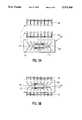
FIG. 3A & 3B are an assembly view and a plan view of a second embodiment of the present invention.
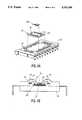
FIG. 4A & 4B provide an assembly view and a cross-sectional view of the assembly of a preferred embodiment of the present invention.
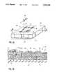
FIG. 2A is a prospective view of an example of the chip carrier of the preferred embodiment of the present invention. Thechip carrier 100 has one ormore chip locations 102 on atop surface 104 for mounting Integrated Circuit (IC) chips 106. Although thecarrier 100 in the example on FIG. 2A shows fourchip mounting locations 102, the number of mountinglocations 102 shown is exemplary and not intended to be limiting, as it is contemplated that the number of mountinglocations 102 may be more or less than four. Eachchip mounting location 102 has a plurality of signal andpower pads 108 for physically transferring power, data, control etc., between thecarrier 100 and theIC chip 106 mounted therein. Integrated Circuit chips 106 are mounted on thecarrier 100 inchip mounting locations 102 by a plurality of Controlled Collapsed Chip Connection C4's)solder balls 110.Conductive lands 112 on the top surface, and which may also be on the bottom surface, provide inter-chip wiring to wire together the mountedIC chips 106. Signals and power are provided to the carrier at a plurality of carrier pads 120 (see FIG. 2B), which also are connected toconductive lands 112. In the preferred embodiment of the present invention, theconductive lands 112 are Copper. However, any low resistance conductive material may be used in place of, or, in combination with Copper for signal and power distribution.
A cross-sectional view ofcarrier 100 at B--B is shown in FIG. 2B. Thecarrier 100 may have asingle layer 122 of insulating material with a singleconductive plane 124 on thetop surface 104 or, if required, the carrier may have a secondconductive plane 124 on itsbottom surface 114. Alternatively, the carrier may be a multi-layer structure withconductive planes 124 separated by insulatinglayers 122 as shown in the cross-sectional view of FIG. 2B. If the carrier has more than oneconductive plane 124, signals and power are distributed from the carrier'stop surface 104 through thecarrier 100 to other conductive planes, by interconnect vias orvias 128. Thecarrier 100 of this example has 5 insulatinglayers 122 and aconductive plane 124 sandwiched between each pair of insulatinglayers 122. Including thetop surface 104, thebottom surface 114 and the 4 internal planes of the carrier, there are 6conductive planes 124, each of which may include signal wiring or power distribution. Theconductive planes 124 are functionally identical to the internal layers of a multilayer printed circuit card or a multi-layer ceramic substrate.
In one embodiment of the present invention,carrier solder balls 130 provide a means for directly mounting and connecting .thecarrier 100 onto a printed-circuit board (not shown). Alternatively, Polymer Metal Conductive (PMC) paste may be substituted forsolder balls 130. Thecarrier solder balls 130 may be deposited on thecarrier 100 or on the substrate, module package or printed circuit card. Additionally, although not shown, it is contemplated that the chip signal and power pads may have deposited solder on them or chip C4's 110 may provide solder for mountingchips 106.
In the preferred embodiments of the present invention, the material making up the insulatinglayers 122 is a resin composite material of resin epoxy and fiberglass, namely Fire Retardant-4 (FR-4). FR-4 is the same material used in the printed circuit card manufacture. It will be appreciated by a person of ordinary skill in the art, that any material having sufficient insulating characteristics may be substituted for FR-4.
A second embodiment of the present invention is represented by the example of FIGS. 3A, showing an an assembly view, and 3B, showing a plan view. Since many of the features of the embodiments herein described are common to the embodiment of the example of FIGS. 2A and 2B, in order to minimize confusion, the numbering of common features is carried throughout the specification. Also, since the common features are sufficiently described in relation to FIGS. 2A and 2B, the description of common features will not be repeated.
In the embodiment of FIGS. 3A and 3B, anIC chip 106 is mounted oncarrier 100 as in the preferred embodiment of FIG. 2A and 2B. A lead-frame 140 such as typically used for a Plastic Leaded Chip Container (PLCC) package, is soldered to thecarrier 100 by depositedsolder balls 130 on thecarrier pads 120. FIG. 3B is a plan view of thecarrier 100 attached to thelead frame 140. Alternatively, the lead-frame 140 may be J lead type and solder may be deposited on the J lead lead-frame prior to mounting the carrier. Direct Chip Attach (DCA)organic polymerized encapsulent 142 deposited on thecarrier 100 passivates and protects the C4's 110 and the mountedchip 106. Such a DCA organic polymerized encapsulant is disclosed in U.S. Pat. No. 4,604,644 to Beckham et al., assigned to the assignee of the present invention and incorporated herein by reference.Carriers 100 thus mounted on lead-frame 140 have improved heat transfer and dissipation, because the chips mounted on the carrier are not enclosed in a package.
A third embodiment of the present invention is represented by the assembly view example of FIG. 4A, with FIG. 4B showing a cross-section of the assembly of FIG. 4A. Achip 106 is mounted in achip mounting location 102 on thecarrier 100. In this embodiment, thecarrier pads 108 are on thetop surface 104 and are suitable for wire bond connections. The carrier is not soldered to thepackage 150 as in the previous embodiments. Instead, the carrier is glued into asuitable package 150, such as a PLCC, with any suitable thermal-adhesive glue. Power and signals are transferred to and from the carrier through wire-bonds 152 between carrier connectpads 120 andwire bond pads 154 on thepackage 150. DCAorganic polymerized Encapsulant 156 passivates and protects thechip 106, thecarrier 100 andwire bond pads 154, as well as thewire bonds 152 themselves, which would otherwise be exposed. Alternatively, instead of DCAorganic polymerized encapsulant 156, a standard package top (not shown) may be substituted. Thus, this embodiment of the present invention provides an inexpensive package for very small chips, which might otherwise require more expensive packaging techniques.
From the disclosed embodiments, it can be seen that the present invention provides an inexpensive, flexible packaging alternative for integrated circuit chips. The carrier also provides an inexpensive means of redirecting chip signals, such that two chips with identical function, but incompatible footprints may become interchangeable. This and other variations of the preferred embodiment of the present invention will occur to a person of ordinary skill in the art without departing from the scope and spirit of this invention.
Claims (15)
1. An integrated circuit module comprising:
a carrier, said carrier comprising:
chip mounting means for fixedly mounting at least one integrated circuit chip to said carrier, and
distribution means for distributing said power and said signals to said at least one integrated circuit chip, said distribution means comprised of a plurality of carrier pads connected to a plurality of chip bonding pads by carrier wiring on at least one conductive plane, said conductive plane being on at least one layer of resin fiberglass composite material;
said carrier being selected from at least two carriers with different distribution means, whereby two chips with identical function, but incompatible footprints, become interchangeable in an integrated circuit chip;
the integrated circuit chip package; and,
bonding means for mounting and connecting the carrier to said package.
2. The integrated circuit chip module of claim 1 wherein said at least one conductive plane comprises a plurality of conductive planes, and, each adjacent pair of said conductive planes being separated by one said at least one layer.
3. The distribution means of the carrier of claim 2 wherein at least two of said plurality of conductive planes are internal conductive planes and said at least one layer is a plurality of insulating layers, whereby each said insulating layer is sandwiched between a pair of said conductive planes.
4. The integrated circuit chip module of claim 3 wherein the chip mounting means comprises a deposited solder ball on each said chip bonding pad, whereby said deposited solder balls fixedly attach and electrically connect said each chip to said carrier.
5. The integrated circuit chip module of claim 3 wherein each said integrated circuit chip has a plurality of chip pads, and the chip mounting means comprises:
glue;
a plurality of wire bonds between the chip bonding pads and the chip pads; and,
an organic encapsulant, whereby said chips are glued to said carrier and wire bonds are encased in said organic encapsulant.
6. The integrated circuit chip module of claim 3 wherein said integrated circuit chip package is a leaded chip carrier with a cavity and a plurality of package wire bond pads, and said chip mounting means comprises:
a plurality of carrier wire bond pads; and
a wire bond between each of said carrier wire bond pads and one of said package wire bond pads, whereby said carrier is fixedly mounted in said cavity.
7. The integrated circuit package of claim 3 wherein the bonding means are Polymer Metal Conductive Paste.
8. The integrated circuit chip package of claim 7 wherein the chip mounting means are Polymer Metal Conductive Paste.
9. An integrated circuit package comprising:
a carrier, said carrier comprising:
a plurality of wiring planes,
a plurality of insulating layers of resin fiberglass composite material, each said insulating layer being sandwiched between an adjacent pair of said wiring planes,
a plurality of vias, each of said vias extending from one of said wiring planes through at least one of said insulating layers to a second of said wiring planes,
a plurality of carrier pads, and
at least one chip mounting location on a surface of said carrier, said mounting location having a plurality of chip power and signal pads;
said carrier being selected from at least two different carriers, the mounting location of one said carrier having a different chip power and signal assignment than the other said carrier, whereby two chips with identical functions, but incompatible footprints, become interchangeable in said package; and
means for providing signal and power to said carrier.
10. The integrated circuit chip package of claim 9 wherein said means for providing signals and power is a lead frame fixedly mounted to said carrier at said carrier pads.
11. The integrated circuit package of claim 9 wherein said means for providing signal and power comprise:
a leaded chip carrier with a cavity, a plurality of wire bond pads, and a plurality of package leads, said carrier being fixedly mounted in said cavity; and,
a plurality of wire bonds connected between said plurality of carrier pads and said plurality wire bond pads.
12. The integrated circuit package of claim 9 wherein every integrated circuit chip mounted in said at least once chip mounting location is coated and protected by a deposited encapsulant.
13. The integrated circuit chip package of claim 11, wherein said carrier pads, said wire bond pads and said plurality of wire bonds are coated and passivated by a deposited encapsulant.
14. The integrated circuit chip package of claim 9 wherein said means for providing signals and power are Polymer Metal Conductive Paste.
15. The integrated circuit chip package of claim 14 wherein each said mounting location's chip power and signal pads have Polymer Metal Conductive Paste deposited thereon.
Priority Applications (3)
| Application Number | Priority Date | Filing Date | Title |
|---|---|---|---|
| US07/929,631US5313366A (en) | 1992-08-12 | 1992-08-12 | Direct chip attach module (DCAM) |
| JP5161625AJP2561793B2 (en) | 1992-08-12 | 1993-06-30 | Direct chip attach module |
| EP93202299AEP0592022A1 (en) | 1992-08-12 | 1993-08-04 | A direct chip attach module (DCAM) |
Applications Claiming Priority (1)
| Application Number | Priority Date | Filing Date | Title |
|---|---|---|---|
| US07/929,631US5313366A (en) | 1992-08-12 | 1992-08-12 | Direct chip attach module (DCAM) |
Publications (1)
| Publication Number | Publication Date |
|---|---|
| US5313366Atrue US5313366A (en) | 1994-05-17 |
Family
ID=25458188
Family Applications (1)
| Application Number | Title | Priority Date | Filing Date |
|---|---|---|---|
| US07/929,631Expired - LifetimeUS5313366A (en) | 1992-08-12 | 1992-08-12 | Direct chip attach module (DCAM) |
Country Status (3)
| Country | Link |
|---|---|
| US (1) | US5313366A (en) |
| EP (1) | EP0592022A1 (en) |
| JP (1) | JP2561793B2 (en) |
Cited By (55)
| Publication number | Priority date | Publication date | Assignee | Title |
|---|---|---|---|---|
| US5426263A (en)* | 1993-12-23 | 1995-06-20 | Motorola, Inc. | Electronic assembly having a double-sided leadless component |
| US5748452A (en)* | 1996-07-23 | 1998-05-05 | International Business Machines Corporation | Multi-electronic device package |
| US5926379A (en)* | 1995-12-07 | 1999-07-20 | Sagem Sa | Electronic card assembly by means of solder connections |
| US5991161A (en)* | 1997-12-19 | 1999-11-23 | Intel Corporation | Multi-chip land grid array carrier |
| US6031728A (en)* | 1997-12-23 | 2000-02-29 | Aerospatiale Societe Nationale Industrielle | Device and method for interconnection between two electronic devices |
| US6077725A (en)* | 1992-09-03 | 2000-06-20 | Lucent Technologies Inc | Method for assembling multichip modules |
| US6081429A (en)* | 1999-01-20 | 2000-06-27 | Micron Technology, Inc. | Test interposer for use with ball grid array packages assemblies and ball grid array packages including same and methods |
| US6133634A (en)* | 1998-08-05 | 2000-10-17 | Fairchild Semiconductor Corporation | High performance flip chip package |
| US6259408B1 (en) | 1999-11-19 | 2001-07-10 | Intermec Ip Corp. | RFID transponders with paste antennas and flip-chip attachment |
| US6303992B1 (en) | 1999-07-06 | 2001-10-16 | Visteon Global Technologies, Inc. | Interposer for mounting semiconductor dice on substrates |
| US6317333B1 (en)* | 1997-08-28 | 2001-11-13 | Mitsubishi Denki Kabushiki Kaisha | Package construction of semiconductor device |
| US6319829B1 (en) | 1999-08-18 | 2001-11-20 | International Business Machines Corporation | Enhanced interconnection to ceramic substrates |
| US6399892B1 (en) | 2000-09-19 | 2002-06-04 | International Business Machines Corporation | CTE compensated chip interposer |
| US6423623B1 (en) | 1998-06-09 | 2002-07-23 | Fairchild Semiconductor Corporation | Low Resistance package for semiconductor devices |
| US6429509B1 (en) | 1999-05-03 | 2002-08-06 | United Microelectronics Corporation | Integrated circuit with improved interconnect structure and process for making same |
| US20020162215A1 (en)* | 2001-03-14 | 2002-11-07 | Kledzik Kenneth J. | Method and apparatus for fabricating a circuit board with a three dimensional surface mounted array of semiconductor chips |
| US20020181216A1 (en)* | 2000-03-13 | 2002-12-05 | Kledzik Kenneth J. | Electronic module having a three dimensional array of carrier-mounted integrated circuit packages |
| WO2002101831A1 (en)* | 2001-05-14 | 2002-12-19 | Sony Corporation | Semiconductor device and its manufacturing method |
| US20030001247A1 (en)* | 2001-06-18 | 2003-01-02 | International Rectifier Corporation | High voltage semiconductor device housing with increased clearance between housing can and die for improved flux flushing |
| US20030057544A1 (en)* | 2001-09-13 | 2003-03-27 | Nathan Richard J. | Integrated assembly protocol |
| US20030059976A1 (en)* | 2001-09-24 | 2003-03-27 | Nathan Richard J. | Integrated package and methods for making same |
| US20030132531A1 (en)* | 2001-03-28 | 2003-07-17 | Martin Standing | Surface mounted package with die bottom spaced from support board |
| US20030153119A1 (en)* | 2002-02-14 | 2003-08-14 | Nathan Richard J. | Integrated circuit package and method for fabrication |
| US20030165051A1 (en)* | 2000-03-13 | 2003-09-04 | Kledzik Kenneth J. | Modular integrated circuit chip carrier |
| US20040007762A1 (en)* | 2002-07-11 | 2004-01-15 | Lameres Brock J. | Method for fabricating adaptor for aligning and electrically coupling circuit devices having dissimilar connectivity patterns |
| US20040099940A1 (en)* | 2002-11-22 | 2004-05-27 | International Rectifier Corporation | Semiconductor device having clips for connecting to external elements |
| US6768646B1 (en)* | 1998-01-23 | 2004-07-27 | Texas Instruments Incorporated | High density internal ball grid array integrated circuit package |
| US6890798B2 (en)* | 1999-06-08 | 2005-05-10 | Intel Corporation | Stacked chip packaging |
| US6903458B1 (en)* | 2002-06-20 | 2005-06-07 | Richard J. Nathan | Embedded carrier for an integrated circuit chip |
| US20050186707A1 (en)* | 2000-04-04 | 2005-08-25 | International Rectifier Corp. | Chip scale surface mounted device and process of manufacture |
| US20050250352A1 (en)* | 2002-09-25 | 2005-11-10 | Philippe Maugars | Connector for chip-card |
| US6967412B2 (en) | 2001-08-24 | 2005-11-22 | International Rectifier Corporation | Wafer level underfill and interconnect process |
| US20050269677A1 (en)* | 2004-05-28 | 2005-12-08 | Martin Standing | Preparation of front contact for surface mounting |
| US7030466B1 (en) | 1999-05-03 | 2006-04-18 | United Microelectronics Corporation | Intermediate structure for making integrated circuit device and wafer |
| US20060107524A1 (en)* | 2000-10-16 | 2006-05-25 | Jason Engle | Method and apparatus for fabricating a circuit board with a three dimensional surface mounted array of semiconductor chips |
| US20060164820A1 (en)* | 2005-01-12 | 2006-07-27 | Mecker Donald W | Radial circuit board, system, and methods |
| US7119447B2 (en) | 2001-03-28 | 2006-10-10 | International Rectifier Corporation | Direct fet device for high frequency application |
| US20060240598A1 (en)* | 2005-04-20 | 2006-10-26 | International Rectifier Corporation | Chip scale package |
| US20070012947A1 (en)* | 2002-07-15 | 2007-01-18 | International Rectifier Corporation | Direct FET device for high frequency application |
| US7179740B1 (en) | 1999-05-03 | 2007-02-20 | United Microelectronics Corporation | Integrated circuit with improved interconnect structure and process for making same |
| US20080017797A1 (en)* | 2006-07-21 | 2008-01-24 | Zhaohui Cheng | Pattern inspection and measurement apparatus |
| US20080042252A1 (en)* | 1998-06-30 | 2008-02-21 | Micron Technology, Inc. | Stackable ceramic fbga for high thermal applications |
| US7368325B2 (en) | 2005-04-21 | 2008-05-06 | International Rectifier Corporation | Semiconductor package |
| US7405471B2 (en) | 2000-10-16 | 2008-07-29 | Legacy Electronics, Inc. | Carrier-based electronic module |
| US20080192452A1 (en)* | 2007-02-12 | 2008-08-14 | Randall Michael S | Passive electronic device |
| US7579697B2 (en) | 2002-07-15 | 2009-08-25 | International Rectifier Corporation | Arrangement for high frequency application |
| US20090267171A1 (en)* | 2008-04-24 | 2009-10-29 | Micron Technology, Inc. | Pre-encapsulated cavity interposer |
| US20100061056A1 (en)* | 2008-09-08 | 2010-03-11 | Damion Searls | Mainboard assembly including a package overlying a die directly attached to the mainboard |
| USRE41559E1 (en) | 2001-10-10 | 2010-08-24 | International Rectifier Corporation | Semiconductor device package with improved cooling |
| US20110156730A1 (en)* | 2006-11-03 | 2011-06-30 | Pillai Edward R | Chip-based prober for high frequency measurements and methods of measuring |
| US20110215443A1 (en)* | 1996-12-02 | 2011-09-08 | Kabushiki Kaisha Toshiba | Multichip semiconductor device, chip therefor and method of formation thereof |
| US8466546B2 (en) | 2005-04-22 | 2013-06-18 | International Rectifier Corporation | Chip-scale package |
| US20160309592A1 (en)* | 2015-04-20 | 2016-10-20 | Rohm Co., Ltd. | Printed Wiring Board |
| US11482472B2 (en) | 2018-06-13 | 2022-10-25 | Intel Corporation | Thermal management solutions for stacked integrated circuit devices |
| US11688665B2 (en) | 2018-06-13 | 2023-06-27 | Intel Corporation | Thermal management solutions for stacked integrated circuit devices |
Families Citing this family (10)
| Publication number | Priority date | Publication date | Assignee | Title |
|---|---|---|---|---|
| US5412539A (en)* | 1993-10-18 | 1995-05-02 | Hughes Aircraft Company | Multichip module with a mandrel-produced interconnecting decal |
| GB2307334A (en)* | 1995-11-16 | 1997-05-21 | Marconi Gec Ltd | Electronic component packaging |
| FR2750798B1 (en)* | 1996-07-02 | 1998-11-06 | Sgs Thomson Microelectronics | LOW COST BOX FOR INTEGRATED CIRCUITS MADE IN SMALL QUANTITY |
| US6117759A (en)* | 1997-01-03 | 2000-09-12 | Motorola Inc. | Method for multiplexed joining of solder bumps to various substrates during assembly of an integrated circuit package |
| US6373717B1 (en) | 1999-07-02 | 2002-04-16 | International Business Machines Corporation | Electronic package with high density interconnect layer |
| US6351393B1 (en) | 1999-07-02 | 2002-02-26 | International Business Machines Corporation | Electronic package for electronic components and method of making same |
| CA2455024A1 (en) | 2003-01-30 | 2004-07-30 | Endicott Interconnect Technologies, Inc. | Stacked chip electronic package having laminate carrier and method of making same |
| US7035113B2 (en) | 2003-01-30 | 2006-04-25 | Endicott Interconnect Technologies, Inc. | Multi-chip electronic package having laminate carrier and method of making same |
| US7023707B2 (en) | 2003-01-30 | 2006-04-04 | Endicott Interconnect Technologies, Inc. | Information handling system |
| US7332818B2 (en) | 2005-05-12 | 2008-02-19 | Endicott Interconnect Technologies, Inc. | Multi-chip electronic package with reduced line skew and circuitized substrate for use therein |
Citations (13)
| Publication number | Priority date | Publication date | Assignee | Title |
|---|---|---|---|---|
| US4034468A (en)* | 1976-09-03 | 1977-07-12 | Ibm Corporation | Method for making conduction-cooled circuit package |
| US4074342A (en)* | 1974-12-20 | 1978-02-14 | International Business Machines Corporation | Electrical package for lsi devices and assembly process therefor |
| US4193082A (en)* | 1978-06-23 | 1980-03-11 | International Business Machines Corporation | Multi-layer dielectric structure |
| US4202007A (en)* | 1978-06-23 | 1980-05-06 | International Business Machines Corporation | Multi-layer dielectric planar structure having an internal conductor pattern characterized with opposite terminations disposed at a common edge surface of the layers |
| US4415025A (en)* | 1981-08-10 | 1983-11-15 | International Business Machines Corporation | Thermal conduction element for semiconductor devices |
| JPS6110263A (en)* | 1984-06-26 | 1986-01-17 | Nec Kansai Ltd | Hybrid ic |
| US4682270A (en)* | 1984-05-18 | 1987-07-21 | British Telecommunications Public Limited Company | Integrated circuit chip carrier |
| US4803595A (en)* | 1986-11-17 | 1989-02-07 | International Business Machines Corporation | Interposer chip technique for making engineering changes between interconnected semiconductor chips |
| US4821142A (en)* | 1986-06-06 | 1989-04-11 | Hitachi, Ltd. | Ceramic multilayer circuit board and semiconductor module |
| US4827328A (en)* | 1986-03-17 | 1989-05-02 | Fujitsu Limited | Hybrid IC device |
| US5048178A (en)* | 1990-10-23 | 1991-09-17 | International Business Machines Corp. | Alignment--registration tool for fabricating multi-layer electronic packages |
| US5110664A (en)* | 1989-07-10 | 1992-05-05 | Hitachi, Ltd. | Thick film and thin film composite substrate and electronic circuit apparatus using it |
| US5220489A (en)* | 1991-10-11 | 1993-06-15 | Motorola, Inc. | Multicomponent integrated circuit package |
Family Cites Families (3)
| Publication number | Priority date | Publication date | Assignee | Title |
|---|---|---|---|---|
| JPS6059756A (en)* | 1983-09-12 | 1985-04-06 | Ibiden Co Ltd | Plug-in package and manufacture thereof |
| JPS62204550A (en)* | 1986-03-05 | 1987-09-09 | Shinko Electric Ind Co Ltd | Printed substrate type semiconductor package |
| FR2666173A1 (en)* | 1990-08-21 | 1992-02-28 | Thomson Csf | HYBRID INTERCONNECTION STRUCTURE FOR INTEGRATED CIRCUITS AND MANUFACTURING METHOD. |
- 1992
- 1992-08-12USUS07/929,631patent/US5313366A/ennot_activeExpired - Lifetime
- 1993
- 1993-06-30JPJP5161625Apatent/JP2561793B2/ennot_activeExpired - Lifetime
- 1993-08-04EPEP93202299Apatent/EP0592022A1/ennot_activeWithdrawn
Patent Citations (13)
| Publication number | Priority date | Publication date | Assignee | Title |
|---|---|---|---|---|
| US4074342A (en)* | 1974-12-20 | 1978-02-14 | International Business Machines Corporation | Electrical package for lsi devices and assembly process therefor |
| US4034468A (en)* | 1976-09-03 | 1977-07-12 | Ibm Corporation | Method for making conduction-cooled circuit package |
| US4193082A (en)* | 1978-06-23 | 1980-03-11 | International Business Machines Corporation | Multi-layer dielectric structure |
| US4202007A (en)* | 1978-06-23 | 1980-05-06 | International Business Machines Corporation | Multi-layer dielectric planar structure having an internal conductor pattern characterized with opposite terminations disposed at a common edge surface of the layers |
| US4415025A (en)* | 1981-08-10 | 1983-11-15 | International Business Machines Corporation | Thermal conduction element for semiconductor devices |
| US4682270A (en)* | 1984-05-18 | 1987-07-21 | British Telecommunications Public Limited Company | Integrated circuit chip carrier |
| JPS6110263A (en)* | 1984-06-26 | 1986-01-17 | Nec Kansai Ltd | Hybrid ic |
| US4827328A (en)* | 1986-03-17 | 1989-05-02 | Fujitsu Limited | Hybrid IC device |
| US4821142A (en)* | 1986-06-06 | 1989-04-11 | Hitachi, Ltd. | Ceramic multilayer circuit board and semiconductor module |
| US4803595A (en)* | 1986-11-17 | 1989-02-07 | International Business Machines Corporation | Interposer chip technique for making engineering changes between interconnected semiconductor chips |
| US5110664A (en)* | 1989-07-10 | 1992-05-05 | Hitachi, Ltd. | Thick film and thin film composite substrate and electronic circuit apparatus using it |
| US5048178A (en)* | 1990-10-23 | 1991-09-17 | International Business Machines Corp. | Alignment--registration tool for fabricating multi-layer electronic packages |
| US5220489A (en)* | 1991-10-11 | 1993-06-15 | Motorola, Inc. | Multicomponent integrated circuit package |
Non-Patent Citations (16)
| Title |
|---|
| Disclosed Anonymously, Organic Card Device Carrier Research Disclosure, Kenneth Mason Publications, Ltd., May 1990, No. 313.* |
| E. Berndlmaier, et al., High Performance Package IBM Technical Disclosure Bulletin, vol. 20, No. 8, p. 3090 (Jan. 1978).* |
| F. Motika, "Flip-Chip on Personalization Chip Carrier Package" IBM Technical Disclosure Bulletin, vol. 23, No. 7A, Dec. 1980 pp. 2770-2773. |
| F. Motika, Flip Chip on Personalization Chip Carrier Package IBM Technical Disclosure Bulletin, vol. 23, No. 7A, Dec. 1980 pp. 2770 2773.* |
| J. A. Curtis, et al., "High-Performance Multi-Chip Carrier" IBM Technical Disclosure Bulletin, vol. 33, No. 2, pp. 15-16 (Jul. 1990). |
| J. A. Curtis, et al., High Performance Multi Chip Carrier IBM Technical Disclosure Bulletin, vol. 33, No. 2, pp. 15 16 (Jul. 1990).* |
| J. Benenati, et al., "Circuit Package" IBM Technical Disclosure Bulletin, vol. 10, No. 12, pp. 1977-1978 (May 1968). |
| J. Benenati, et al., Circuit Package IBM Technical Disclosure Bulletin, vol. 10, No. 12, pp. 1977 1978 (May 1968).* |
| M. T. McMahon, Jr., "Semiconductor Device Carrier for Modules" IBM Technical disclosure Bulletin, vol. 18, No. 5, pp. 1440-1441 (Oct. 1975). |
| M. T. McMahon, Jr., Semiconductor Device Carrier for Modules IBM Technical disclosure Bulletin, vol. 18, No. 5, pp. 1440 1441 (Oct. 1975).* |
| P. Geldermans, "Flexible Solder Connection and Method of Fabricating" IBM Technical Disclosure Bulletin, vol. 18, No. 5, pp. 1379-1380 (Oct. 1975). |
| P. Geldermans, Flexible Solder Connection and Method of Fabricating IBM Technical Disclosure Bulletin, vol. 18, No. 5, pp. 1379 1380 (Oct. 1975).* |
| R. S. Austenfeld, et al. "High Density Direct Chip Attach Substrate Manufacturing Process" IBM Technical Disclosure Bulletin, vol. 34, No. 2, Jul. 1991, pp. 85-86. |
| R. S. Austenfeld, et al. High Density Direct Chip Attach Substrate Manufacturing Process IBM Technical Disclosure Bulletin, vol. 34, No. 2, Jul. 1991, pp. 85 86.* |
| S. B. Greenspan, "C-4 Package for Programmable Read-Only Memory" IBM Technical Disclosure Bulletin, vol. 23, No. 3, pp. 879-880 (Aug. 1980). |
| S. B. Greenspan, C 4 Package for Programmable Read Only Memory IBM Technical Disclosure Bulletin, vol. 23, No. 3, pp. 879 880 (Aug. 1980).* |
Cited By (101)
| Publication number | Priority date | Publication date | Assignee | Title |
|---|---|---|---|---|
| US6077725A (en)* | 1992-09-03 | 2000-06-20 | Lucent Technologies Inc | Method for assembling multichip modules |
| US5426263A (en)* | 1993-12-23 | 1995-06-20 | Motorola, Inc. | Electronic assembly having a double-sided leadless component |
| US5926379A (en)* | 1995-12-07 | 1999-07-20 | Sagem Sa | Electronic card assembly by means of solder connections |
| US6101100A (en)* | 1996-07-23 | 2000-08-08 | International Business Machines Corporation | Multi-electronic device package |
| US5748452A (en)* | 1996-07-23 | 1998-05-05 | International Business Machines Corporation | Multi-electronic device package |
| US20110215443A1 (en)* | 1996-12-02 | 2011-09-08 | Kabushiki Kaisha Toshiba | Multichip semiconductor device, chip therefor and method of formation thereof |
| US8283755B2 (en)* | 1996-12-02 | 2012-10-09 | Kabushiki Kaisha Toshiba | Multichip semiconductor device, chip therefor and method of formation thereof |
| US6317333B1 (en)* | 1997-08-28 | 2001-11-13 | Mitsubishi Denki Kabushiki Kaisha | Package construction of semiconductor device |
| US5991161A (en)* | 1997-12-19 | 1999-11-23 | Intel Corporation | Multi-chip land grid array carrier |
| US6097611A (en)* | 1997-12-19 | 2000-08-01 | Intel Corporation | Multi-chip land grid array carrier |
| US6031728A (en)* | 1997-12-23 | 2000-02-29 | Aerospatiale Societe Nationale Industrielle | Device and method for interconnection between two electronic devices |
| US6768646B1 (en)* | 1998-01-23 | 2004-07-27 | Texas Instruments Incorporated | High density internal ball grid array integrated circuit package |
| US6423623B1 (en) | 1998-06-09 | 2002-07-23 | Fairchild Semiconductor Corporation | Low Resistance package for semiconductor devices |
| US20080042252A1 (en)* | 1998-06-30 | 2008-02-21 | Micron Technology, Inc. | Stackable ceramic fbga for high thermal applications |
| US7829991B2 (en) | 1998-06-30 | 2010-11-09 | Micron Technology, Inc. | Stackable ceramic FBGA for high thermal applications |
| US6133634A (en)* | 1998-08-05 | 2000-10-17 | Fairchild Semiconductor Corporation | High performance flip chip package |
| US7892884B2 (en) | 1998-08-05 | 2011-02-22 | Fairchild Semiconductor Corporation | High performance multi-chip flip chip package |
| US6489678B1 (en) | 1998-08-05 | 2002-12-03 | Fairchild Semiconductor Corporation | High performance multi-chip flip chip package |
| US6294403B1 (en) | 1998-08-05 | 2001-09-25 | Rajeev Joshi | High performance flip chip package |
| US20090230540A1 (en)* | 1998-08-05 | 2009-09-17 | Rajeev Joshi | High performance multi-chip flip chip package |
| US6992384B2 (en) | 1998-08-05 | 2006-01-31 | Fairchild Semiconductor Corporation | High performance multi-chip flip chip package |
| US6627991B1 (en) | 1998-08-05 | 2003-09-30 | Fairchild Semiconductor Corporation | High performance multi-chip flip package |
| US7537958B1 (en) | 1998-08-05 | 2009-05-26 | Fairchild Semiconductor Corporation | High performance multi-chip flip chip package |
| US20040159939A1 (en)* | 1998-08-05 | 2004-08-19 | Fairchild Semiconductor Corporation | High performance multi-chip flip chip package |
| US6081429A (en)* | 1999-01-20 | 2000-06-27 | Micron Technology, Inc. | Test interposer for use with ball grid array packages assemblies and ball grid array packages including same and methods |
| US6452807B1 (en) | 1999-01-20 | 2002-09-17 | Micron Technology, Inc. | Test interposer for use with ball grid array packages, assemblies and ball grid array packages including same, and methods |
| US7179740B1 (en) | 1999-05-03 | 2007-02-20 | United Microelectronics Corporation | Integrated circuit with improved interconnect structure and process for making same |
| US6838310B1 (en) | 1999-05-03 | 2005-01-04 | United Microelectronics Corporation | Integrated circuit with improved interconnect structure and process for making same |
| US7030466B1 (en) | 1999-05-03 | 2006-04-18 | United Microelectronics Corporation | Intermediate structure for making integrated circuit device and wafer |
| US6822316B1 (en) | 1999-05-03 | 2004-11-23 | United Microelectronics Corp. | Integrated circuit with improved interconnect structure and process for making same |
| US6429509B1 (en) | 1999-05-03 | 2002-08-06 | United Microelectronics Corporation | Integrated circuit with improved interconnect structure and process for making same |
| US6890798B2 (en)* | 1999-06-08 | 2005-05-10 | Intel Corporation | Stacked chip packaging |
| US6303992B1 (en) | 1999-07-06 | 2001-10-16 | Visteon Global Technologies, Inc. | Interposer for mounting semiconductor dice on substrates |
| US6319829B1 (en) | 1999-08-18 | 2001-11-20 | International Business Machines Corporation | Enhanced interconnection to ceramic substrates |
| US6259408B1 (en) | 1999-11-19 | 2001-07-10 | Intermec Ip Corp. | RFID transponders with paste antennas and flip-chip attachment |
| US20030165051A1 (en)* | 2000-03-13 | 2003-09-04 | Kledzik Kenneth J. | Modular integrated circuit chip carrier |
| US7796400B2 (en) | 2000-03-13 | 2010-09-14 | Legacy Electronics, Inc. | Modular integrated circuit chip carrier |
| US20020181216A1 (en)* | 2000-03-13 | 2002-12-05 | Kledzik Kenneth J. | Electronic module having a three dimensional array of carrier-mounted integrated circuit packages |
| US20060254809A1 (en)* | 2000-03-13 | 2006-11-16 | Kledzik Kenneth J | Modular integrated circuit chip carrier |
| US6900529B2 (en)* | 2000-03-13 | 2005-05-31 | Legacy Electronics, Inc. | Electronic module having a three dimensional array of carrier-mounted integrated circuit packages |
| US7102892B2 (en) | 2000-03-13 | 2006-09-05 | Legacy Electronics, Inc. | Modular integrated circuit chip carrier |
| US20060220123A1 (en)* | 2000-04-04 | 2006-10-05 | International Rectifier Corporation | Chip scale surface mounted device and process of manufacture |
| US7253090B2 (en) | 2000-04-04 | 2007-08-07 | International Rectifier Corporation | Chip scale surface mounted device and process of manufacture |
| US7476979B2 (en) | 2000-04-04 | 2009-01-13 | International Rectifier Corporation | Chip scale surface mounted device and process of manufacture |
| US7122887B2 (en) | 2000-04-04 | 2006-10-17 | International Rectifier Corporation | Chip scale surface mounted device and process of manufacture |
| US20050186707A1 (en)* | 2000-04-04 | 2005-08-25 | International Rectifier Corp. | Chip scale surface mounted device and process of manufacture |
| US6399892B1 (en) | 2000-09-19 | 2002-06-04 | International Business Machines Corporation | CTE compensated chip interposer |
| US6516513B2 (en) | 2000-09-19 | 2003-02-11 | International Business Machines Corporation | Method of making a CTE compensated chip interposer |
| US7405471B2 (en) | 2000-10-16 | 2008-07-29 | Legacy Electronics, Inc. | Carrier-based electronic module |
| US7337522B2 (en) | 2000-10-16 | 2008-03-04 | Legacy Electronics, Inc. | Method and apparatus for fabricating a circuit board with a three dimensional surface mounted array of semiconductor chips |
| US20060107524A1 (en)* | 2000-10-16 | 2006-05-25 | Jason Engle | Method and apparatus for fabricating a circuit board with a three dimensional surface mounted array of semiconductor chips |
| US7103970B2 (en) | 2001-03-14 | 2006-09-12 | Legacy Electronics, Inc. | Method for fabricating a circuit board with a three dimensional surface mounted array of semiconductor chips |
| US20040194301A1 (en)* | 2001-03-14 | 2004-10-07 | Kledzik Kenneth J. | Method and apparatus for fabricating a circuit board with a three dimensional surface mounted array of semiconductor chips |
| US20020162215A1 (en)* | 2001-03-14 | 2002-11-07 | Kledzik Kenneth J. | Method and apparatus for fabricating a circuit board with a three dimensional surface mounted array of semiconductor chips |
| US7316060B2 (en) | 2001-03-14 | 2008-01-08 | Legacy Electronics, Inc. | System for populating a circuit board with semiconductor chips |
| US7119447B2 (en) | 2001-03-28 | 2006-10-10 | International Rectifier Corporation | Direct fet device for high frequency application |
| US6930397B2 (en) | 2001-03-28 | 2005-08-16 | International Rectifier Corporation | Surface mounted package with die bottom spaced from support board |
| US20030132531A1 (en)* | 2001-03-28 | 2003-07-17 | Martin Standing | Surface mounted package with die bottom spaced from support board |
| US7285866B2 (en) | 2001-03-28 | 2007-10-23 | International Rectifier Corporation | Surface mounted package with die bottom spaced from support board |
| US7064005B2 (en) | 2001-05-14 | 2006-06-20 | Sony Corporation | Semiconductor apparatus and method of manufacturing same |
| WO2002101831A1 (en)* | 2001-05-14 | 2002-12-19 | Sony Corporation | Semiconductor device and its manufacturing method |
| KR100825658B1 (en) | 2001-05-14 | 2008-04-29 | 소니 가부시끼 가이샤 | Semiconductor device and manufacturing method thereof |
| US20040115919A1 (en)* | 2001-05-14 | 2004-06-17 | Yuji Takaoka | Semiconductor device and its manufacturing method |
| US7476964B2 (en) | 2001-06-18 | 2009-01-13 | International Rectifier Corporation | High voltage semiconductor device housing with increased clearance between housing can and die for improved flux flushing |
| US20030001247A1 (en)* | 2001-06-18 | 2003-01-02 | International Rectifier Corporation | High voltage semiconductor device housing with increased clearance between housing can and die for improved flux flushing |
| US6967412B2 (en) | 2001-08-24 | 2005-11-22 | International Rectifier Corporation | Wafer level underfill and interconnect process |
| US20030057544A1 (en)* | 2001-09-13 | 2003-03-27 | Nathan Richard J. | Integrated assembly protocol |
| US20030059976A1 (en)* | 2001-09-24 | 2003-03-27 | Nathan Richard J. | Integrated package and methods for making same |
| USRE41559E1 (en) | 2001-10-10 | 2010-08-24 | International Rectifier Corporation | Semiconductor device package with improved cooling |
| US20030153119A1 (en)* | 2002-02-14 | 2003-08-14 | Nathan Richard J. | Integrated circuit package and method for fabrication |
| US6903458B1 (en)* | 2002-06-20 | 2005-06-07 | Richard J. Nathan | Embedded carrier for an integrated circuit chip |
| US20040007762A1 (en)* | 2002-07-11 | 2004-01-15 | Lameres Brock J. | Method for fabricating adaptor for aligning and electrically coupling circuit devices having dissimilar connectivity patterns |
| US7397137B2 (en) | 2002-07-15 | 2008-07-08 | International Rectifier Corporation | Direct FET device for high frequency application |
| US20070012947A1 (en)* | 2002-07-15 | 2007-01-18 | International Rectifier Corporation | Direct FET device for high frequency application |
| US7579697B2 (en) | 2002-07-15 | 2009-08-25 | International Rectifier Corporation | Arrangement for high frequency application |
| US20050250352A1 (en)* | 2002-09-25 | 2005-11-10 | Philippe Maugars | Connector for chip-card |
| US6841865B2 (en) | 2002-11-22 | 2005-01-11 | International Rectifier Corporation | Semiconductor device having clips for connecting to external elements |
| US20040099940A1 (en)* | 2002-11-22 | 2004-05-27 | International Rectifier Corporation | Semiconductor device having clips for connecting to external elements |
| US20050269677A1 (en)* | 2004-05-28 | 2005-12-08 | Martin Standing | Preparation of front contact for surface mounting |
| US20060164820A1 (en)* | 2005-01-12 | 2006-07-27 | Mecker Donald W | Radial circuit board, system, and methods |
| US7435097B2 (en) | 2005-01-12 | 2008-10-14 | Legacy Electronics, Inc. | Radial circuit board, system, and methods |
| US8097938B2 (en) | 2005-04-20 | 2012-01-17 | International Rectifier Corporation | Conductive chip-scale package |
| US20060240598A1 (en)* | 2005-04-20 | 2006-10-26 | International Rectifier Corporation | Chip scale package |
| US20090174058A1 (en)* | 2005-04-20 | 2009-07-09 | International Rectifier Corporation | Chip scale package |
| US7524701B2 (en) | 2005-04-20 | 2009-04-28 | International Rectifier Corporation | Chip-scale package |
| US7368325B2 (en) | 2005-04-21 | 2008-05-06 | International Rectifier Corporation | Semiconductor package |
| US8061023B2 (en) | 2005-04-21 | 2011-11-22 | International Rectifier Corporation | Process of fabricating a semiconductor package |
| US8466546B2 (en) | 2005-04-22 | 2013-06-18 | International Rectifier Corporation | Chip-scale package |
| US20080017797A1 (en)* | 2006-07-21 | 2008-01-24 | Zhaohui Cheng | Pattern inspection and measurement apparatus |
| US20110156730A1 (en)* | 2006-11-03 | 2011-06-30 | Pillai Edward R | Chip-based prober for high frequency measurements and methods of measuring |
| US20080192452A1 (en)* | 2007-02-12 | 2008-08-14 | Randall Michael S | Passive electronic device |
| US8072082B2 (en) | 2008-04-24 | 2011-12-06 | Micron Technology, Inc. | Pre-encapsulated cavity interposer |
| US8399297B2 (en) | 2008-04-24 | 2013-03-19 | Micron Technology, Inc. | Methods of forming and assembling pre-encapsulated assemblies and of forming associated semiconductor device packages |
| US20090267171A1 (en)* | 2008-04-24 | 2009-10-29 | Micron Technology, Inc. | Pre-encapsulated cavity interposer |
| US20100061056A1 (en)* | 2008-09-08 | 2010-03-11 | Damion Searls | Mainboard assembly including a package overlying a die directly attached to the mainboard |
| US10251273B2 (en) | 2008-09-08 | 2019-04-02 | Intel Corporation | Mainboard assembly including a package overlying a die directly attached to the mainboard |
| US10555417B2 (en) | 2008-09-08 | 2020-02-04 | Intel Corporation | Mainboard assembly including a package overlying a die directly attached to the mainboard |
| US20160309592A1 (en)* | 2015-04-20 | 2016-10-20 | Rohm Co., Ltd. | Printed Wiring Board |
| US10856406B2 (en)* | 2015-04-20 | 2020-12-01 | Rohm Co., Ltd. | Printed wiring board |
| US11482472B2 (en) | 2018-06-13 | 2022-10-25 | Intel Corporation | Thermal management solutions for stacked integrated circuit devices |
| US11688665B2 (en) | 2018-06-13 | 2023-06-27 | Intel Corporation | Thermal management solutions for stacked integrated circuit devices |
Also Published As
| Publication number | Publication date |
|---|---|
| JPH06112271A (en) | 1994-04-22 |
| JP2561793B2 (en) | 1996-12-11 |
| EP0592022A1 (en) | 1994-04-13 |
Similar Documents
| Publication | Publication Date | Title |
|---|---|---|
| US5313366A (en) | Direct chip attach module (DCAM) | |
| US6396136B2 (en) | Ball grid package with multiple power/ground planes | |
| EP0559366B1 (en) | Stackable three-dimensional multiple chip semiconductor device and method for making the same | |
| EP0729180B1 (en) | Packaging multi-chip modules without wirebond interconnection | |
| US6339254B1 (en) | Stacked flip-chip integrated circuit assemblage | |
| US6738263B2 (en) | Stackable ball grid array package | |
| US5789815A (en) | Three dimensional semiconductor package having flexible appendages | |
| US5307240A (en) | Chiplid, multichip semiconductor package design concept | |
| US6326696B1 (en) | Electronic package with interconnected chips | |
| US7400032B2 (en) | Module assembly for stacked BGA packages | |
| EP0638931B1 (en) | Multi-chip module | |
| US5751063A (en) | Multi-chip module | |
| US20070102803A1 (en) | Method for making stacked integrated circuits (ICs) using prepackaged parts | |
| HK1004352B (en) | Stackable three-dimensional multiple chip semiconductor device and method for making the same | |
| JP3726318B2 (en) | Chip size package, manufacturing method thereof, and second level packaging | |
| US20030201521A1 (en) | Semiconductor packaging device and manufacture thereof | |
| JPH07263625A (en) | Vertical IC chip stack with discrete chip carrier formed from dielectric tape | |
| JPH09167813A (en) | Integrated circuit package | |
| US5872397A (en) | Semiconductor device package including a thick integrated circuit chip stack | |
| US4731700A (en) | Semiconductor connection and crossover apparatus | |
| US20020063331A1 (en) | Film carrier semiconductor device | |
| CA2202316A1 (en) | Electronic device assembly | |
| HK1002400A (en) | Packaging multi-chip modules without wirebond interconnection |
Legal Events
| Date | Code | Title | Description |
|---|---|---|---|
| AS | Assignment | Owner name:INTERNATIONAL BUSINESS MACHINES CORPORATION A COR Free format text:ASSIGNMENT OF ASSIGNORS INTEREST.;ASSIGNORS:GAUDENZI, GENE J.;NIHAL, PERWAIZ;REEL/FRAME:006226/0870;SIGNING DATES FROM 19920626 TO 19920710 | |
| STCF | Information on status: patent grant | Free format text:PATENTED CASE | |
| FPAY | Fee payment | Year of fee payment:4 | |
| FPAY | Fee payment | Year of fee payment:8 | |
| FPAY | Fee payment | Year of fee payment:12 |