US5313096A - IC chip package having chip attached to and wire bonded within an overlying substrate - Google Patents
IC chip package having chip attached to and wire bonded within an overlying substrateDownload PDFInfo
- Publication number
- US5313096A US5313096AUS07/920,763US92076392AUS5313096AUS 5313096 AUS5313096 AUS 5313096AUS 92076392 AUS92076392 AUS 92076392AUS 5313096 AUS5313096 AUS 5313096A
- Authority
- US
- United States
- Prior art keywords
- chip
- aperture
- substrate layer
- substrate
- layer
- Prior art date
- Legal status (The legal status is an assumption and is not a legal conclusion. Google has not performed a legal analysis and makes no representation as to the accuracy of the status listed.)
- Expired - Fee Related
Links
Images


Classifications
- H—ELECTRICITY
- H01—ELECTRIC ELEMENTS
- H01L—SEMICONDUCTOR DEVICES NOT COVERED BY CLASS H10
- H01L23/00—Details of semiconductor or other solid state devices
- H01L23/48—Arrangements for conducting electric current to or from the solid state body in operation, e.g. leads, terminal arrangements ; Selection of materials therefor
- H01L23/488—Arrangements for conducting electric current to or from the solid state body in operation, e.g. leads, terminal arrangements ; Selection of materials therefor consisting of soldered or bonded constructions
- H01L23/498—Leads, i.e. metallisations or lead-frames on insulating substrates, e.g. chip carriers
- H01L23/49805—Leads, i.e. metallisations or lead-frames on insulating substrates, e.g. chip carriers the leads being also applied on the sidewalls or the bottom of the substrate, e.g. leadless packages for surface mounting
- H—ELECTRICITY
- H01—ELECTRIC ELEMENTS
- H01L—SEMICONDUCTOR DEVICES NOT COVERED BY CLASS H10
- H01L23/00—Details of semiconductor or other solid state devices
- H01L23/12—Mountings, e.g. non-detachable insulating substrates
- H01L23/13—Mountings, e.g. non-detachable insulating substrates characterised by the shape
- H—ELECTRICITY
- H01—ELECTRIC ELEMENTS
- H01L—SEMICONDUCTOR DEVICES NOT COVERED BY CLASS H10
- H01L25/00—Assemblies consisting of a plurality of semiconductor or other solid state devices
- H01L25/03—Assemblies consisting of a plurality of semiconductor or other solid state devices all the devices being of a type provided for in a single subclass of subclasses H10B, H10D, H10F, H10H, H10K or H10N, e.g. assemblies of rectifier diodes
- H01L25/10—Assemblies consisting of a plurality of semiconductor or other solid state devices all the devices being of a type provided for in a single subclass of subclasses H10B, H10D, H10F, H10H, H10K or H10N, e.g. assemblies of rectifier diodes the devices having separate containers
- H01L25/105—Assemblies consisting of a plurality of semiconductor or other solid state devices all the devices being of a type provided for in a single subclass of subclasses H10B, H10D, H10F, H10H, H10K or H10N, e.g. assemblies of rectifier diodes the devices having separate containers the devices being integrated devices of class H10
- H—ELECTRICITY
- H05—ELECTRIC TECHNIQUES NOT OTHERWISE PROVIDED FOR
- H05K—PRINTED CIRCUITS; CASINGS OR CONSTRUCTIONAL DETAILS OF ELECTRIC APPARATUS; MANUFACTURE OF ASSEMBLAGES OF ELECTRICAL COMPONENTS
- H05K13/00—Apparatus or processes specially adapted for manufacturing or adjusting assemblages of electric components
- H05K13/04—Mounting of components, e.g. of leadless components
- H05K13/046—Surface mounting
- H05K13/0465—Surface mounting by soldering
- H—ELECTRICITY
- H01—ELECTRIC ELEMENTS
- H01L—SEMICONDUCTOR DEVICES NOT COVERED BY CLASS H10
- H01L2224/00—Indexing scheme for arrangements for connecting or disconnecting semiconductor or solid-state bodies and methods related thereto as covered by H01L24/00
- H01L2224/01—Means for bonding being attached to, or being formed on, the surface to be connected, e.g. chip-to-package, die-attach, "first-level" interconnects; Manufacturing methods related thereto
- H01L2224/42—Wire connectors; Manufacturing methods related thereto
- H01L2224/47—Structure, shape, material or disposition of the wire connectors after the connecting process
- H01L2224/48—Structure, shape, material or disposition of the wire connectors after the connecting process of an individual wire connector
- H01L2224/4805—Shape
- H01L2224/4809—Loop shape
- H01L2224/48091—Arched
- H—ELECTRICITY
- H01—ELECTRIC ELEMENTS
- H01L—SEMICONDUCTOR DEVICES NOT COVERED BY CLASS H10
- H01L2224/00—Indexing scheme for arrangements for connecting or disconnecting semiconductor or solid-state bodies and methods related thereto as covered by H01L24/00
- H01L2224/01—Means for bonding being attached to, or being formed on, the surface to be connected, e.g. chip-to-package, die-attach, "first-level" interconnects; Manufacturing methods related thereto
- H01L2224/42—Wire connectors; Manufacturing methods related thereto
- H01L2224/47—Structure, shape, material or disposition of the wire connectors after the connecting process
- H01L2224/48—Structure, shape, material or disposition of the wire connectors after the connecting process of an individual wire connector
- H01L2224/481—Disposition
- H01L2224/48151—Connecting between a semiconductor or solid-state body and an item not being a semiconductor or solid-state body, e.g. chip-to-substrate, chip-to-passive
- H01L2224/48221—Connecting between a semiconductor or solid-state body and an item not being a semiconductor or solid-state body, e.g. chip-to-substrate, chip-to-passive the body and the item being stacked
- H01L2224/48225—Connecting between a semiconductor or solid-state body and an item not being a semiconductor or solid-state body, e.g. chip-to-substrate, chip-to-passive the body and the item being stacked the item being non-metallic, e.g. insulating substrate with or without metallisation
- H01L2224/48237—Connecting between a semiconductor or solid-state body and an item not being a semiconductor or solid-state body, e.g. chip-to-substrate, chip-to-passive the body and the item being stacked the item being non-metallic, e.g. insulating substrate with or without metallisation connecting the wire to a die pad of the item
- H—ELECTRICITY
- H01—ELECTRIC ELEMENTS
- H01L—SEMICONDUCTOR DEVICES NOT COVERED BY CLASS H10
- H01L2224/00—Indexing scheme for arrangements for connecting or disconnecting semiconductor or solid-state bodies and methods related thereto as covered by H01L24/00
- H01L2224/01—Means for bonding being attached to, or being formed on, the surface to be connected, e.g. chip-to-package, die-attach, "first-level" interconnects; Manufacturing methods related thereto
- H01L2224/42—Wire connectors; Manufacturing methods related thereto
- H01L2224/47—Structure, shape, material or disposition of the wire connectors after the connecting process
- H01L2224/48—Structure, shape, material or disposition of the wire connectors after the connecting process of an individual wire connector
- H01L2224/481—Disposition
- H01L2224/48151—Connecting between a semiconductor or solid-state body and an item not being a semiconductor or solid-state body, e.g. chip-to-substrate, chip-to-passive
- H01L2224/48221—Connecting between a semiconductor or solid-state body and an item not being a semiconductor or solid-state body, e.g. chip-to-substrate, chip-to-passive the body and the item being stacked
- H01L2224/48225—Connecting between a semiconductor or solid-state body and an item not being a semiconductor or solid-state body, e.g. chip-to-substrate, chip-to-passive the body and the item being stacked the item being non-metallic, e.g. insulating substrate with or without metallisation
- H01L2224/4824—Connecting between the body and an opposite side of the item with respect to the body
- H—ELECTRICITY
- H01—ELECTRIC ELEMENTS
- H01L—SEMICONDUCTOR DEVICES NOT COVERED BY CLASS H10
- H01L2225/00—Details relating to assemblies covered by the group H01L25/00 but not provided for in its subgroups
- H01L2225/03—All the devices being of a type provided for in the same main group of the same subclass of class H10, e.g. assemblies of rectifier diodes
- H01L2225/10—All the devices being of a type provided for in the same main group of the same subclass of class H10, e.g. assemblies of rectifier diodes the devices having separate containers
- H01L2225/1005—All the devices being of a type provided for in the same main group of the same subclass of class H10, e.g. assemblies of rectifier diodes the devices having separate containers the devices being integrated devices of class H10
- H01L2225/1011—All the devices being of a type provided for in the same main group of the same subclass of class H10, e.g. assemblies of rectifier diodes the devices having separate containers the devices being integrated devices of class H10 the containers being in a stacked arrangement
- H01L2225/1017—All the devices being of a type provided for in the same main group of the same subclass of class H10, e.g. assemblies of rectifier diodes the devices having separate containers the devices being integrated devices of class H10 the containers being in a stacked arrangement the lowermost container comprising a device support
- H01L2225/1023—All the devices being of a type provided for in the same main group of the same subclass of class H10, e.g. assemblies of rectifier diodes the devices having separate containers the devices being integrated devices of class H10 the containers being in a stacked arrangement the lowermost container comprising a device support the support being an insulating substrate
- H—ELECTRICITY
- H01—ELECTRIC ELEMENTS
- H01L—SEMICONDUCTOR DEVICES NOT COVERED BY CLASS H10
- H01L2225/00—Details relating to assemblies covered by the group H01L25/00 but not provided for in its subgroups
- H01L2225/03—All the devices being of a type provided for in the same main group of the same subclass of class H10, e.g. assemblies of rectifier diodes
- H01L2225/10—All the devices being of a type provided for in the same main group of the same subclass of class H10, e.g. assemblies of rectifier diodes the devices having separate containers
- H01L2225/1005—All the devices being of a type provided for in the same main group of the same subclass of class H10, e.g. assemblies of rectifier diodes the devices having separate containers the devices being integrated devices of class H10
- H01L2225/1011—All the devices being of a type provided for in the same main group of the same subclass of class H10, e.g. assemblies of rectifier diodes the devices having separate containers the devices being integrated devices of class H10 the containers being in a stacked arrangement
- H01L2225/1047—Details of electrical connections between containers
- H01L2225/1064—Electrical connections provided on a side surface of one or more of the containers
- H—ELECTRICITY
- H01—ELECTRIC ELEMENTS
- H01L—SEMICONDUCTOR DEVICES NOT COVERED BY CLASS H10
- H01L24/00—Arrangements for connecting or disconnecting semiconductor or solid-state bodies; Methods or apparatus related thereto
- H01L24/01—Means for bonding being attached to, or being formed on, the surface to be connected, e.g. chip-to-package, die-attach, "first-level" interconnects; Manufacturing methods related thereto
- H01L24/42—Wire connectors; Manufacturing methods related thereto
- H01L24/47—Structure, shape, material or disposition of the wire connectors after the connecting process
- H01L24/48—Structure, shape, material or disposition of the wire connectors after the connecting process of an individual wire connector
- H—ELECTRICITY
- H01—ELECTRIC ELEMENTS
- H01L—SEMICONDUCTOR DEVICES NOT COVERED BY CLASS H10
- H01L2924/00—Indexing scheme for arrangements or methods for connecting or disconnecting semiconductor or solid-state bodies as covered by H01L24/00
- H01L2924/0001—Technical content checked by a classifier
- H01L2924/00014—Technical content checked by a classifier the subject-matter covered by the group, the symbol of which is combined with the symbol of this group, being disclosed without further technical details
- H—ELECTRICITY
- H01—ELECTRIC ELEMENTS
- H01L—SEMICONDUCTOR DEVICES NOT COVERED BY CLASS H10
- H01L2924/00—Indexing scheme for arrangements or methods for connecting or disconnecting semiconductor or solid-state bodies as covered by H01L24/00
- H01L2924/01—Chemical elements
- H01L2924/01039—Yttrium [Y]
- H—ELECTRICITY
- H01—ELECTRIC ELEMENTS
- H01L—SEMICONDUCTOR DEVICES NOT COVERED BY CLASS H10
- H01L2924/00—Indexing scheme for arrangements or methods for connecting or disconnecting semiconductor or solid-state bodies as covered by H01L24/00
- H01L2924/10—Details of semiconductor or other solid state devices to be connected
- H01L2924/11—Device type
- H01L2924/14—Integrated circuits
- H—ELECTRICITY
- H01—ELECTRIC ELEMENTS
- H01L—SEMICONDUCTOR DEVICES NOT COVERED BY CLASS H10
- H01L2924/00—Indexing scheme for arrangements or methods for connecting or disconnecting semiconductor or solid-state bodies as covered by H01L24/00
- H01L2924/15—Details of package parts other than the semiconductor or other solid state devices to be connected
- H01L2924/181—Encapsulation
Definitions
- the present inventionrelates to the high density packaging and stacking of integrated circuit chips to achieve, for example, an increased memory capacity in a memory circuit.
- CMOScomplementary metal-oxide-semiconductor
- CMOScomplementary metal-oxide-semiconductor
- the printed circuit boardsare typically arranged in a parallel relationship, with each board being disposed adjacent to and spaced from the other boards. If the chip packages are arranged in a single level on each circuit board, then a relatively large amount of space is required, particularly for large capacity memory systems. Moreover, the space between adjacent printed circuit boards is largely unused.
- the chip carriersare stacked, one above the other, such that the various conductors of the chip carriers are in alignment and are electrically connected to one another.
- the resultis a relatively dense stack of chips wired in parallel.
- each chipis connected to a different set of aligned enable signal conductors so as to be enabled independently of all of the other chips in the stack.
- the chip packages or carriers used to accomplish chip stackingcan assume various different forms.
- An example of a chip package or carrier which is externally configurableis described in a copending patent application, Ser. No. 07/552,578 of John Forthun, filed Jul. 13, 1990 and commonly assigned with the present application.
- the Forthun applicationdescribes a chip carrier having a central cavity in which the chip is encapsulated.
- a carrier terminal provided on the outside of the chip carrieris electrically coupled to a circuit terminal on the chip such that the electrical coupling has a removable external configuration link.
- the configuration of an electronic circuit formed by the chipcan be altered by removing the configuration link to break the electrical connection between the carrier terminal and the circuit terminal on the chip.
- chip packages or carriers described in the Eide patent and in the Forthun applicationprovide relatively compact chip packaging so that high density chip stacking can be accomplished on a printed circuit board, increased packaging density continues to be a desirable goal.
- additional chip packaging configurations and methods of making such chip packageswhich provide certain additional advantages not present in the prior art. For example, it would be desirable to be able to lap the chip or die to a desired thickness after being made part of a chip package, and it would be desirable to be able to program the package with a bonding wire after package test. The stacking of pre-tested partially packaged chips would also be a desirable feature.
- a chip packagein which the upper active surface of the chip is attached to the bottom of a multilayer substrate comprised of at least a lower layer and an upper layer.
- Various terminals on the active surface of the chipare wire bonded inwardly through a plurality of apertures in the lower substrate layer to bonding pads on an upper surface of the lower substrate layer.
- the bonding padsare coupled by metallized strips to conductors arranged along opposite side edges of the substrate for parallel electrical connection when a stack of the chip packages is formed. Because the chip terminals are wire bonded inwardly through apertures in the lower substrate layer, such wire bonding is confined within the outer periphery of the chip so as to confine the wire bonding within the X-Y plane of the three dimensional chip package. In this manner, the size of the chip package is minimized, and a stack of the chip packages can be formed within a very small space to provide a very high chip density.
- the substrateis comprised of lower and upper layers of relatively thin, generally planar configurations which are joined together during formation of the substrate.
- the lower substrate layerhas opposite apertures extending through the thickness thereof to receive bonding wires coupling the terminals on the upper active surface of the chip to bonding pads on an upper surface of the lower substrate layer.
- the chipis also of thin, planar configuration. Metallized strips on the upper surface of the lower substrate layer couple the bonding pads to conductive pads at the opposite outer edges of the lower substrate layer.
- the upper active layer of the chipis attached to the lower surface of the lower substrate layer.
- the upper substrate layerhas three apertures extending through the thickness thereof.
- a third aperture in the upper substrate layerprovides access to a bonding option array on the upper surface of the lower substrate layer.
- the bonding option arrayincludes a chip enable trace which is coupled via wire bond to a chip enable terminal on the active surface of the chip at one end of the substrate. By virtue of such access the chip enable trace is wire bonded to a selected one of a plurality of optional bonding pads within the bonding option array to complete connection to a selected input/output pad at the edge of the substrate during testing and programming of the chip assembly.
- the third aperture in the upper substrate layeris then filled with epoxy which is cured and then ground flat at the upper surface of the upper substrate layer.
- the chip and the multilayer substrateare provided as separate elements.
- the upper active side of the chipis attached to the lower surface of the lower substrate layer with an appropriate adhesive such as epoxy.
- the terminals on the active surface of the chipare wire bonded to the bonding pads on the upper surface of the lower substrate layer so that the bonding wires pass through the apertures adjacent the opposite ends of the lower substrate layer.
- the apertures in the lower substrate layer and the corresponding apertures in the upper substrate layerare then filled with epoxy.
- the upper surface of the upper substrate layeris ground to make the epoxy flush with such surface.
- the lower surface of the chipis lapped as necessary to provide the chip with a desired thickness.
- the chip packageis then electrically tested at various different temperatures.
- One or more input/output (I/O) pinscan be programmed by virtue of off-chip wire bonding. This is accomplished by wire bonding the chip enable trace to a selected one of the optimal bonding pads in the bonding option array. The position of the chip within a final stack assembly need not be determined until after the tests are performed and the associated yield loss determined.
- the third aperture in the upper substrate layeris filled with epoxy which is cured and then ground flush with the upper surface of the upper substrate layer.
- the chip packagesare then assembled into a stack.
- the conductive pads at the opposite edges of the substrate of each packageare formed into vertical arrays of conductors in the stack by soldering, wire bonding or other appropriate connection.
- the resultis a stack of partially packaged but fully tested chips.
- the stackitself can be tested and repaired as necessary. Thereafter, the stack is attached to a lead frame or substrate and encapsulated using transfer molding or other packaging techniques.
- the ability to lap the chip in package form after handling in a thick form as part of the assembled chip packageis advantageous. Also advantageous is the ability to post-test package programming with bonding wire, and the ability to form a stack of pretested partially packaged chips.
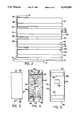
- FIG. 1is a perspective view of a portion of a chip stack employing a plurality of chip packages in accordance with the invention
- FIG. 2is a side view of a portion of the chip stack of FIG. 1;
- FIG. 3is a plan view of a chip used in each of the chip packages in the stack of FIGS. 1 and 2;
- FIG. 4is a plan view of a lower substrate layer forming a part of a multilayer substrate used in each of the chip packages of the chip stack of FIGS. 1 and 2;
- FIG. 5is a plan view of an upper substrate layer forming another part of the multilayer substrate used in each of the chip packages of the chip stack of FIGS. 1 and 2;
- FIG. 6is a perspective view, partly broken-away, of a portion of one of the chip packages of the chip stack of FIGS. 1 and 2;
- FIG. 7is a sectional view of the chip package of FIG. 6 taken along the lines 7--7 thereof;
- FIG. 8is an enlarged plan view of the lower substrate layer of FIG. 4 after the chip of FIG. 3 has been attached to the multilayer substrate and wire bonding at the opposite ends has been accomplished;
- FIG. 9is a side view of a chip and substrate illustrating a prior art wire bonding arrangement
- FIG. 10is a side view of a chip and substrate illustrating inward wire bonding in accordance with the present invention.
- FIG. 11is a diagram of the successive steps employed in a method of making a chip package and a stack thereof in accordance with the invention.
- FIG. 1shows a chip stack 10 including a plurality of chip packages 12 in accordance with the invention.
- the chip stack 10may be comprised of practically any number of the chip packages 12 that is desired, the example of FIG. 1 comprises four of the chip packages 12.
- the chip packages 12are stacked in a vertical array on top of a lead frame or substrate 14.
- Vertical strips of solder 16extend along side surfaces 18 of the individual chip packages 12 to couple conductive pads on the chip packages 12 in parallel. Such interconnections are shown in greater detail in FIG. 2, to which reference is now made.
- FIG. 2is a side view of the vertical stack of the chip packages 12 shown in FIG. 1.
- each chip package 12is comprised of an IC chip or die 20 disposed beneath a substrate 22.
- the substrate 22is multilayer in nature and is comprised of a lower substrate layer 24 disposed immediately above and attached to the chip 20, and an upper substrate layer 26 disposed over the lower substrate layer 24.
- the chip 20 of each chip package 12is disposed on top of the upper substrate layer 26 of the chip package 12 immediately below.
- the lower and upper substrate layers 24 and 26are separately shown and described herein for clarity of illustration.
- the layers 24 and 26are joined together as part of the process of forming the substrate 22, before the chip 20 is attached thereto.
- Each chip package 12has a plurality of conductive films 28 spaced along the side surface 18 thereof. As described hereafter, each conductive film 28 is in electrical contact with a different conductive pad within the substrate 22 of the chip package 12.
- the conductive film 28is attached to opposite conductive pads 30 and 32 at upper and lower surfaces respectively of the substrate 22 to form a generally U-shaped electrical contacts during formation of the substrate 22.
- the solder strips 16 of FIG. 1contact the conductive film 28 and the opposite conductive pads 30 and 32 of each chip package 12, to form a vertical conductor array, as shown in FIG. 2.
- each chip package 12is shown in FIGS. 3, 4 and 5 respectively.
- the chip 20is rectangular in shape and of relatively thin, generally planar configuration.
- An upper active surface 34 of the chip 20includes a plurality of electrical terminals 36 in conventional fashion.
- the terminals 36are concentrated at opposite ends of the chip 20, and include a chip enable terminal 37.
- the lower substrate layer 24is shown in FIG. 4 as being a rectangular element of relatively thin, generally planar configuration as is the upper substrate layer 26 of FIG. 5.
- the lower and upper substrate layers 24 and 26are of like length and width, but different in thickness, with the upper substrate layer 26 being thicker than the lower substrate layer 24.
- the lower substrate layer 24is slightly longer and wider than the chip 20, so that apertures 38 and 40 adjacent the opposite ends thereof overlie the electrical terminals 36 at the opposite ends of the chip 20 when the active surface 34 of the chip 20 is attached to a lower surface 42 at the underside of the lower substrate layer 24.
- the lower surface 42 of the lower substrate layer 24is shown in FIG. 2.
- the lower substrate layer 24has an upper surface 46 opposite the lower surface 42 thereof.
- the upper surface 46has a plurality of conductive pads 48 mounted thereon along opposite side edges 50 and 52 of the lower substrate layer 24 and forming input/output (I/O) terminals for the chip package 12.
- the conductive pads 48make electrical contact with the conductive films 28 on the side edges 18 of the chip packages 12 to couple corresponding ones of the conductive pads 48 within the different chip packages 12 in parallel.
- the upper surface 46 of the lower substrate layer 24also includes a plurality of metallized strips 54 which extend from the conductive pads 48 to the edges of the apertures 38 and 40 and to a bonding option array 55 at a central region of the lower substrate layer 24.
- the metallized strips 54which extend to the apertures 38 and 40 terminate in bonding pads 56 at the edges of the apertures. The remaining metallized strips 54 terminate at optional bonding pads 57 within the bonding option array 55.
- a metallized strip 59which-forms a main chip enable trace couples a central terminal 61 within the bonding option array 55 to a chip enable bonding pad 63 at the edge of the aperture 40.
- the chip enable bonding pad 63is wire bonded to the chip enable terminal 37 on the chip 20, as described hereafter.
- the upper substrate layer 26is provided with opposite apertures 58 and 60 and an intermediate aperture 62.
- the upper substrate layer 26has an upper surface 64 shown in FIG. 5 and an opposite lower surface 66 shown in FIG. 2.
- the apertures 58 and 60overlay the apertures 38 and 40 in the lower substrate layer 24.
- the intermediate aperture 62 in the upper substrate layer 26overlays the bonding option array 55 on the lower substrate layer 24.
- the various conductive pads 30are mounted along the upper surface 64 at opposite side edges 68 and 70 of the upper substrate layer 26.
- the conductive pads 32 shown in FIG. 2are mounted along the lower surface 42 of the lower substrate layer 24 at the opposite side edges 50 and 52 thereof, in similar fashion.
- the conductive pads 30 and 32are joined by the conductive films 28 during formation of the substrate 22.
- the lower and upper substrate layers 24 and 26are separately shown and described herein for clarity of illustration, and are joined together to form the substrate 22 before the chip 20 is attached thereto.
- the layers 24 and 26are co-fired together in the same manner as layers in a standard multilayer hybrid substrate.
- FIG. 6is a perspective, partly broken-away view of the chip package 12.
- the upper active surface 34 of the chip 20is attached to the lower surface 42 of the lower substrate layer 24.
- the terminals 36 on the active surface 34are exposed by the aperture 38 in the lower substrate layer 24 and the aperture 58 in the upper substrate layer 26.
- Each terminal 36 on the active surface 34 of the chip 20is attached by a bonding wire 72 to a bonding-pad 56 at the end of one of the metallized strips 54 on the upper surface 46 of the lower substrate layer 24.
- the chip enable terminal 37is wire bonded to the chip enable bonding pad 63 in similar fashion.
- the apertures 38 and 58are filled with a quantity of epoxy 74 which has been ground flush with the upper surface 64 of the upper substrate layer 26.
- Several of the conductive pads 30 on the upper surface 64 of the upper substrate layer 26are shown in FIG. 6.
- FIG. 7is a sectional view of the chip package 12 taken along the line 7--7 of FIG. 6. This further illustrates the manner in which each terminal 36 at the upper active surface 34 of the chip 20 is coupled by a bonding wire 72 to a bonding pad 56 at an edge of the aperture 38 in the lower substrate layer 24.
- the apertures 38 and 58are filled with the epoxy 74.
- FIG. 8is an enlarged plan view of the lower substrate layer 24.
- the chip 20 which is attached to the lower surface 42 of the lower substrate layer 24is shown in dotted outline in FIG. 8.
- FIG. 8illustrates the manner in which the various terminals 36 on the upper active surface 34 of the chip 20 are coupled through the apertures 38 and 40 to the bonding pads 56 by the bonding wires 72.
- the bonding pads 56 at the edges of the apertures 38 and 40are coupled by the metallized strips 54 to the conductive pads 48 at the opposite side edges 50 and 52 of the lower substrate layer 24.
- One of the bonding wires 72couples the chip enable terminal 37 to the chip enable bonding pad 63 at the end of the metallized strip 59.
- the aperture 62 in the upper substrate layer 26exposes the bonding option array 55 with the optional bonding pads 57 disposed adjacent and on opposite sides of the central terminal 61.
- a bonding wire 65is used to couple a selected one of the optional bonding pads 57 to the central terminal 61, as shown in FIG. 8. Thereafter, the aperture 62 is filled with epoxy which is cured and then ground flat at the upper surface 64 of the upper substrate layer 26.
- FIG. 9depicts a typical prior art arrangement in which a chip 76 is mounted on the top of a substrate 78.
- the chip 76has terminals 80 and 82 which are coupled by bonding wires 84 and 86 respectively to bonding pads 88 and 90 respectively on an upper surface 92 of the substrate 78. Because of such outward bonding, the width W 1 of the lateral space taken up by the chip 76 and the bonding wires 84 and 86 is substantial.
- the inward bonding of the electrical terminals 36 of the chip 20 through apertures 38 and 40 to the bonding pads 56 on the upper surface 46 of the lower substrate layer 24defines a width W 2 which is no greater than the width of the chip 20. It is this reduction in the X - Y plane of the chip package 12 that provides for substantially greater chip density within the chip stack 10.
- the various side edges of the chip 20lie within planes defining an outer periphery of the chip 20.
- the bonding wires 72are confined within such planar outer periphery of the chip 20.
- FIG. 11shows the successive steps of a preferred method of making the chip stack 10 and the chip packages 12 in accordance with the invention.
- the chip 20 and the substrate 22are separately formed.
- the formed substrate 22comprises the lower and upper layers 24 and 26 joined together to form the integral substrate.
- the upper active surface 34 of the chip 20is attached to the lower surface 42 of the lower substrate layer 24. This is accomplished using epoxy or other appropriate adhesive.
- the terminals 36 on the upper active surface 34 of the chip 20are wire bonded to the bonding pads 56 on the upper surface 46 of the lower substrate layer 24 using the bonding wires 72.
- the bonding wires 72extend through the apertures 38 and 40 in the lower substrate layer 24.
- the chip enable terminal 37is wire bonded to the chip enable bonding pad 63 through the aperture 38.
- the apertures 38 and 40 in the lower substrate layer 24 and the overlying apertures 58 and 60 in the upper substrate layer 26are filled with epoxy which is then cured.
- the upper surface 64 of the upper substrate layer 26is ground to remove excess epoxy. This is accomplished by grinding the surface 64 so that it is flat.
- a lower surface 108 of the chip 20 opposite the upper active surface 34 thereofis lapped to provide the chip 20 with a desired thickness.
- the chip 20is lapped to a thickness of 0.005 inches.
- the substrate 22has a thickness of approximately 0.021 inches. This results in the chip package 12 having a total thickness of less than 0.030 inches.
- the chip 20 of the present examplehas a length of approximately 0.550 inches and a width of approximately 0.225 inches.
- the substrate 22has a length of approximately 0.650 inches and a width of approximately 0.300 inches.
- a seventh step 110 of the method shown in FIG. 11the chip package 12 as so produced is electrically tested. Testing is carried out at various different temperatures, and determines whether the chip package 12 is acceptable or whether it should be rejected. The testing also determines the operating speed of the chip package 12 and other factors such as whether it should be classified as high power or low power. Later, when a chip stack is formed, chip packages with similar operating speed characteristics are assembled together.
- the chip packageis programmed by connecting a length of bonding wire, such as the bonding wire 65 shown in FIG. 8, between the central terminal 61 and a desired one of the optional bonding pads 57 within the bonding option array 55.
- the aperture 62 in the control region of the upper layer 26 of the substrate 22provides the necessary access. This has the effect of coupling the chip enable terminal 37 to a desired I/O terminal in the form of one of the conductive pads 48 on the upper surface 46 of the lower substrate layer 24.
- the aperture 62 in the upper substrate layer 26is filled with epoxy and cured.
- the upper surface 64 of the upper substrate layer 26is ground to remove excess epoxy and make the surface 64 flat.
- a stack of the chip packages 12is assembled to form the chip stack 10.
- the electrical terminals formed by the conductive film 28 together with the conductive pads 30 and 32 at the opposite edges of the substrate 22 of each chip package 12are vertically connected by soldering to form the solder strips 16 shown in FIG. 1.
- the stack of chip packages 12is secured to the lead frame 14.
- the stack of chip packages 12is thereafter encapsulated using transfer molding or other conventional packaging techniques to form the completed chip stack 10.
- Programmingmay then take place, with the main chip enable trace being wire bonded to a desired one of the optional bonding pads. This is advantageously done with the chip already encapsulated within the chip package and thereby protected.
- a stack of the pretested and partially packaged chipsis then formed, with the stack being attached to a frame and encapsulated. The stack can be later disassembled to replace a faulty chip.
Landscapes
- Engineering & Computer Science (AREA)
- Microelectronics & Electronic Packaging (AREA)
- Power Engineering (AREA)
- Physics & Mathematics (AREA)
- Condensed Matter Physics & Semiconductors (AREA)
- General Physics & Mathematics (AREA)
- Computer Hardware Design (AREA)
- Manufacturing & Machinery (AREA)
- Wire Bonding (AREA)
- Tests Of Electronic Circuits (AREA)
- Lead Frames For Integrated Circuits (AREA)
Abstract
Description
Claims (19)
Priority Applications (1)
| Application Number | Priority Date | Filing Date | Title |
|---|---|---|---|
| US07/920,763US5313096A (en) | 1992-03-16 | 1992-07-29 | IC chip package having chip attached to and wire bonded within an overlying substrate |
Applications Claiming Priority (2)
| Application Number | Priority Date | Filing Date | Title |
|---|---|---|---|
| US85175592A | 1992-03-16 | 1992-03-16 | |
| US07/920,763US5313096A (en) | 1992-03-16 | 1992-07-29 | IC chip package having chip attached to and wire bonded within an overlying substrate |
Related Parent Applications (1)
| Application Number | Title | Priority Date | Filing Date |
|---|---|---|---|
| US85175592ADivision | 1992-03-16 | 1992-03-16 |
Publications (1)
| Publication Number | Publication Date |
|---|---|
| US5313096Atrue US5313096A (en) | 1994-05-17 |
Family
ID=25311601
Family Applications (1)
| Application Number | Title | Priority Date | Filing Date |
|---|---|---|---|
| US07/920,763Expired - Fee RelatedUS5313096A (en) | 1992-03-16 | 1992-07-29 | IC chip package having chip attached to and wire bonded within an overlying substrate |
Country Status (4)
| Country | Link |
|---|---|
| US (1) | US5313096A (en) |
| EP (1) | EP0631691A4 (en) |
| JP (1) | JPH07504786A (en) |
| WO (1) | WO1993019485A1 (en) |
Cited By (104)
| Publication number | Priority date | Publication date | Assignee | Title |
|---|---|---|---|---|
| US5373189A (en)* | 1992-08-13 | 1994-12-13 | Commissariate A L'energie Atomique | Three-dimensional multichip module |
| US5432729A (en)* | 1993-04-23 | 1995-07-11 | Irvine Sensors Corporation | Electronic module comprising a stack of IC chips each interacting with an IC chip secured to the stack |
| US5517057A (en)* | 1994-12-20 | 1996-05-14 | International Business Machines Corporation | Electronic modules with interconnected surface metallization layers |
| US5561622A (en)* | 1993-09-13 | 1996-10-01 | International Business Machines Corporation | Integrated memory cube structure |
| US5612570A (en)* | 1995-04-13 | 1997-03-18 | Dense-Pac Microsystems, Inc. | Chip stack and method of making same |
| US5648684A (en)* | 1995-07-26 | 1997-07-15 | International Business Machines Corporation | Endcap chip with conductive, monolithic L-connect for multichip stack |
| US5661087A (en)* | 1994-06-23 | 1997-08-26 | Cubic Memory, Inc. | Vertical interconnect process for silicon segments |
| US5668409A (en)* | 1995-06-05 | 1997-09-16 | Harris Corporation | Integrated circuit with edge connections and method |
| US5726492A (en)* | 1995-10-27 | 1998-03-10 | Fujitsu Limited | Semiconductor module including vertically mounted semiconductor chips |
| US5798963A (en)* | 1995-03-31 | 1998-08-25 | Hyundai Electronics Industries Co., Ltd. | Integrated circuit static write--read and erase semiconductor memory |
| US5818698A (en)* | 1995-10-12 | 1998-10-06 | Micron Technology, Inc. | Method and apparatus for a chip-on-board semiconductor module |
| US5818107A (en)* | 1997-01-17 | 1998-10-06 | International Business Machines Corporation | Chip stacking by edge metallization |
| US5835396A (en)* | 1996-10-17 | 1998-11-10 | Zhang; Guobiao | Three-dimensional read-only memory |
| US5847448A (en)* | 1990-12-11 | 1998-12-08 | Thomson-Csf | Method and device for interconnecting integrated circuits in three dimensions |
| US5869353A (en)* | 1997-11-17 | 1999-02-09 | Dense-Pac Microsystems, Inc. | Modular panel stacking process |
| US5892287A (en)* | 1997-08-18 | 1999-04-06 | Texas Instruments | Semiconductor device including stacked chips having metal patterned on circuit surface and on edge side of chip |
| US5956234A (en)* | 1998-01-20 | 1999-09-21 | Integrated Device Technology, Inc. | Method and structure for a surface mountable rigid-flex printed circuit board |
| US6072233A (en)* | 1998-05-04 | 2000-06-06 | Micron Technology, Inc. | Stackable ball grid array package |
| US6121576A (en)* | 1998-09-02 | 2000-09-19 | Micron Technology, Inc. | Method and process of contact to a heat softened solder ball array |
| USRE36916E (en)* | 1995-03-21 | 2000-10-17 | Simple Technology Incorporated | Apparatus for stacking semiconductor chips |
| US6156165A (en)* | 1997-01-17 | 2000-12-05 | International Business Machines Corporation | Method of forming a metallization feature on an edge of an IC chip |
| US6180881B1 (en) | 1998-05-05 | 2001-01-30 | Harlan Ruben Isaak | Chip stack and method of making same |
| US6242285B1 (en) | 1998-07-23 | 2001-06-05 | Kyung Suk Kang | Stacked package of semiconductor package units via direct connection between leads and stacking method therefor |
| US20010005042A1 (en)* | 1992-12-11 | 2001-06-28 | Burns Carmen D. | Method of manufacturing a surface mount package |
| US6281577B1 (en)* | 1996-06-28 | 2001-08-28 | Pac Tech-Packaging Technologies Gmbh | Chips arranged in plurality of planes and electrically connected to one another |
| US6313998B1 (en) | 1999-04-02 | 2001-11-06 | Legacy Electronics, Inc. | Circuit board assembly having a three dimensional array of integrated circuit packages |
| US6323060B1 (en) | 1999-05-05 | 2001-11-27 | Dense-Pac Microsystems, Inc. | Stackable flex circuit IC package and method of making same |
| US6351029B1 (en) | 1999-05-05 | 2002-02-26 | Harlan R. Isaak | Stackable flex circuit chip package and method of making same |
| US20020047199A1 (en)* | 2000-09-11 | 2002-04-25 | Shinji Ohuchi | Semiconductor device, manufacturing method of semiconductor device, stack type semiconductor device, and manufacturing method of stack type semiconductor device |
| US6404043B1 (en) | 2000-06-21 | 2002-06-11 | Dense-Pac Microsystems, Inc. | Panel stacking of BGA devices to form three-dimensional modules |
| US20020142515A1 (en)* | 2001-03-27 | 2002-10-03 | Staktek Group, L.P. | Contact member stacking system and method |
| US6465893B1 (en) | 1990-09-24 | 2002-10-15 | Tessera, Inc. | Stacked chip assembly |
| US20030002267A1 (en)* | 2001-06-15 | 2003-01-02 | Mantz Frank E. | I/O interface structure |
| US6512303B2 (en) | 1995-12-19 | 2003-01-28 | Micron Technology, Inc. | Flip chip adaptor package for bare die |
| US20030025211A1 (en)* | 2001-07-24 | 2003-02-06 | Ted Bruce | Chip stack with differing chip package types |
| US20030051911A1 (en)* | 2001-09-20 | 2003-03-20 | Roeters Glen E. | Post in ring interconnect using 3-D stacking |
| US6573461B2 (en) | 2001-09-20 | 2003-06-03 | Dpac Technologies Corp | Retaining ring interconnect used for 3-D stacking |
| US20030107118A1 (en)* | 2001-10-09 | 2003-06-12 | Tessera, Inc. | Stacked packages |
| US6608763B1 (en) | 2000-09-15 | 2003-08-19 | Staktek Group L.P. | Stacking system and method |
| US20030192171A1 (en)* | 2002-01-16 | 2003-10-16 | Fey Kate E. | Space-saving packaging of electronic circuits |
| US6660561B2 (en) | 2000-06-15 | 2003-12-09 | Dpac Technologies Corp. | Method of assembling a stackable integrated circuit chip |
| US20030232462A1 (en)* | 2002-06-18 | 2003-12-18 | Poo Chia Yong | Semiconductor devices and semiconductor device components with peripherally located, castellated contacts, assemblies and packages including such semiconductor devices or packages and associated methods |
| US20040031972A1 (en)* | 2001-10-09 | 2004-02-19 | Tessera, Inc. | Stacked packages |
| US20040099938A1 (en)* | 2002-09-11 | 2004-05-27 | Tessera, Inc. | Assemblies having stacked semiconductor chips and methods of making same |
| US20040104470A1 (en)* | 2002-08-16 | 2004-06-03 | Tessera, Inc. | Microelectronic packages with self-aligning features |
| US20040108584A1 (en)* | 2002-12-05 | 2004-06-10 | Roeters Glen E. | Thin scale outline package |
| US20040124523A1 (en)* | 2002-06-18 | 2004-07-01 | Poo Chia Yong | Semiconductor devices including peripherally located bond pads, intermediates thereof, assemblies, and packages including the semiconductor devices, and support elements for the semiconductor devices |
| US20040201111A1 (en)* | 2003-04-09 | 2004-10-14 | Thurgood Blaine J. | Interposer substrates with multisegment interconnect slots, semiconductor die packages including same, semiconductor dice for use therewith and methods of fabrication |
| US20040207990A1 (en)* | 2003-04-21 | 2004-10-21 | Rose Andrew C. | Stair-step signal routing |
| US20040217461A1 (en)* | 2002-08-05 | 2004-11-04 | Tessera, Inc. | Microelectronic adaptors, assemblies and methods |
| US6849480B1 (en) | 1999-05-07 | 2005-02-01 | Seagate Technology Llc | Surface mount IC stacking method and device |
| FR2858912A1 (en)* | 2003-08-11 | 2005-02-18 | Wavecom | ELECTRONIC MODULE FORMED OF STACKED AND SOLIDARIZED COMPONENTS, COMPONENT, METHOD, MEANS OF ASSEMBLY AND ASSEMBLY MACHINE |
| US6861290B1 (en)* | 1995-12-19 | 2005-03-01 | Micron Technology, Inc. | Flip-chip adaptor package for bare die |
| US20050067680A1 (en)* | 2003-09-30 | 2005-03-31 | Boon Suan Jeung | Castellated chip-scale packages and methods for fabricating the same |
| US6885106B1 (en) | 2001-01-11 | 2005-04-26 | Tessera, Inc. | Stacked microelectronic assemblies and methods of making same |
| US6897090B2 (en) | 1994-12-29 | 2005-05-24 | Tessera, Inc. | Method of making a compliant integrated circuit package |
| US20050121758A1 (en)* | 2003-12-04 | 2005-06-09 | Palo Alto Research Center, Inc. | Thin package for stacking integrated circuits |
| US20050173796A1 (en)* | 2001-10-09 | 2005-08-11 | Tessera, Inc. | Microelectronic assembly having array including passive elements and interconnects |
| US20050224952A1 (en)* | 2004-04-13 | 2005-10-13 | Al Vindasius | Three dimensional six surface conformal die coating |
| US20050258530A1 (en)* | 2004-04-13 | 2005-11-24 | Al Vindasius | Micropede stacked die component assembly |
| US6979784B1 (en)* | 2003-10-17 | 2005-12-27 | Advanced Micro Devices, Inc. | Component power interface board |
| US20060001142A1 (en)* | 2002-08-28 | 2006-01-05 | Micron Technology, Inc. | Castellation wafer level packaging of integrated circuit chips |
| US7066741B2 (en) | 1999-09-24 | 2006-06-27 | Staktek Group L.P. | Flexible circuit connector for stacked chip module |
| US7081373B2 (en) | 2001-12-14 | 2006-07-25 | Staktek Group, L.P. | CSP chip stack with flex circuit |
| US20060209023A1 (en)* | 2004-12-30 | 2006-09-21 | Lg Electronics Inc. | Image navigation in a mobile station |
| US20060284286A1 (en)* | 2005-06-20 | 2006-12-21 | Texas Instrument Inc. | Flashless molding of integrated circuit devices |
| US20070075045A1 (en)* | 2005-09-29 | 2007-04-05 | Hans-Joachim Kuhrt | Electrical switch |
| US7215018B2 (en) | 2004-04-13 | 2007-05-08 | Vertical Circuits, Inc. | Stacked die BGA or LGA component assembly |
| US20070165457A1 (en)* | 2005-09-30 | 2007-07-19 | Jin-Ki Kim | Nonvolatile memory system |
| US7304382B2 (en) | 2006-01-11 | 2007-12-04 | Staktek Group L.P. | Managed memory component |
| US20080042252A1 (en)* | 1998-06-30 | 2008-02-21 | Micron Technology, Inc. | Stackable ceramic fbga for high thermal applications |
| US20080042250A1 (en)* | 2006-08-18 | 2008-02-21 | Tessera, Inc. | Stacked microelectronic assemblies and methods therefor |
| US20080042274A1 (en)* | 2002-09-06 | 2008-02-21 | Tessera, Inc. | Components, methods and assemblies for stacked packages |
| US20080067657A1 (en)* | 2006-09-19 | 2008-03-20 | Taiwan Semiconductor Manufacturing Co., Ltd. | Integrated circuit devices with multi-dimensional pad structures |
| US20080088014A1 (en)* | 2006-09-26 | 2008-04-17 | Adkisson James W | Stacked imager package |
| US20080122113A1 (en)* | 2006-08-17 | 2008-05-29 | Corisis David J | Semiconductor device assemblies and systems including at least one conductive pathway extending around a side of at least one semiconductor device and methods for forming the same |
| US7468553B2 (en) | 2006-10-20 | 2008-12-23 | Entorian Technologies, Lp | Stackable micropackages and stacked modules |
| US20090008795A1 (en)* | 2007-07-02 | 2009-01-08 | Tessera, Inc. | Stackable microelectronic device carriers, stacked device carriers and methods of making the same |
| US20090020887A1 (en)* | 2007-07-20 | 2009-01-22 | Shinko Electric Industries Co., Ltd. | Semiconductor apparatus and manufacturing method thereof |
| US7508058B2 (en) | 2006-01-11 | 2009-03-24 | Entorian Technologies, Lp | Stacked integrated circuit module |
| US7508069B2 (en) | 2006-01-11 | 2009-03-24 | Entorian Technologies, Lp | Managed memory component |
| US20090085184A1 (en)* | 2007-09-28 | 2009-04-02 | Samsung Electronics Co., Ltd. | Semiconductor package and method of fabricating the same |
| US7576995B2 (en) | 2005-11-04 | 2009-08-18 | Entorian Technologies, Lp | Flex circuit apparatus and method for adding capacitance while conserving circuit board surface area |
| US7605454B2 (en) | 2006-01-11 | 2009-10-20 | Entorian Technologies, Lp | Memory card and method for devising |
| US7608920B2 (en) | 2006-01-11 | 2009-10-27 | Entorian Technologies, Lp | Memory card and method for devising |
| US20090267171A1 (en)* | 2008-04-24 | 2009-10-29 | Micron Technology, Inc. | Pre-encapsulated cavity interposer |
| US7732905B2 (en) | 2005-07-06 | 2010-06-08 | Samsung Electronics Co., Ltd. | Stack package and semiconductor module implementing the same |
| US20100276572A1 (en)* | 2005-06-02 | 2010-11-04 | Sony Corporation | Semiconductor image sensor module and method of manufacturing the same |
| US20110013373A1 (en)* | 2009-07-14 | 2011-01-20 | Apple Inc. | Systems and methods for providing vias through a modular component |
| USRE43112E1 (en) | 1998-05-04 | 2012-01-17 | Round Rock Research, Llc | Stackable ball grid array package |
| US20120011713A1 (en)* | 2010-07-13 | 2012-01-19 | Foxconn Advanced Technology Inc. | Method for manufacturing multilayer printed circuit board |
| USD680119S1 (en)* | 2011-11-15 | 2013-04-16 | Connectblue Ab | Module |
| USD680545S1 (en)* | 2011-11-15 | 2013-04-23 | Connectblue Ab | Module |
| US8451621B2 (en) | 2010-09-15 | 2013-05-28 | Semiconductor Components Industries, Llc | Semiconductor component and method of manufacture |
| USD689053S1 (en)* | 2011-11-15 | 2013-09-03 | Connectblue Ab | Module |
| USD692896S1 (en)* | 2011-11-15 | 2013-11-05 | Connectblue Ab | Module |
| US20140027895A1 (en)* | 2011-03-31 | 2014-01-30 | Fujitsu Limited | Three-dimensional mounting semiconductor device and method of manufacturing three-dimensional mounting semiconductor device |
| US8654601B2 (en) | 2005-09-30 | 2014-02-18 | Mosaid Technologies Incorporated | Memory with output control |
| US8743610B2 (en) | 2005-09-30 | 2014-06-03 | Conversant Intellectual Property Management Inc. | Method and system for accessing a flash memory device |
| USRE45463E1 (en) | 2003-11-12 | 2015-04-14 | Tessera, Inc. | Stacked microelectronic assemblies with central contacts |
| US20150349012A1 (en)* | 2013-02-14 | 2015-12-03 | Olympus Corporation | Solid-state image pickup device and image pickup device |
| US20150380813A1 (en)* | 2014-06-30 | 2015-12-31 | International Business Machines Corporation | Wireless communication device with joined semiconductors |
| US10129986B2 (en) | 2014-09-24 | 2018-11-13 | Koninklijke Philips N.V. | Printed circuit board and printed circuit board arrangement |
| US11367709B2 (en)* | 2018-06-05 | 2022-06-21 | PAC Tech—Packaging Technologies GmbH | Semiconductor chip stack arrangement and semiconductor chip for producing such a semiconductor chip stack arrangement |
Families Citing this family (1)
| Publication number | Priority date | Publication date | Assignee | Title |
|---|---|---|---|---|
| US5387477A (en)* | 1992-07-17 | 1995-02-07 | Dreisbach Electromotive Inc. | Air manager system for metal-air battery |
Citations (9)
| Publication number | Priority date | Publication date | Assignee | Title |
|---|---|---|---|---|
| US3959579A (en)* | 1974-08-19 | 1976-05-25 | International Business Machines Corporation | Apertured semi-conductor device mounted on a substrate |
| US4379259A (en)* | 1980-03-12 | 1983-04-05 | National Semiconductor Corporation | Process of performing burn-in and parallel functional testing of integrated circuit memories in an environmental chamber |
| JPS61137335A (en)* | 1984-12-10 | 1986-06-25 | Toshiba Corp | Semiconductor device |
| US4956694A (en)* | 1988-11-04 | 1990-09-11 | Dense-Pac Microsystems, Inc. | Integrated circuit chip stacking |
| US4996587A (en)* | 1989-04-10 | 1991-02-26 | International Business Machines Corporation | Integrated semiconductor chip package |
| US5041395A (en)* | 1989-04-07 | 1991-08-20 | Sgs-Thomson Microelectronics S.A. | Method of encapsulating an integrated circuit using a punched metal grid attached to a perforated dielectric strip |
| US5086018A (en)* | 1991-05-02 | 1992-02-04 | International Business Machines Corporation | Method of making a planarized thin film covered wire bonded semiconductor package |
| US5107328A (en)* | 1991-02-13 | 1992-04-21 | Micron Technology, Inc. | Packaging means for a semiconductor die having particular shelf structure |
| US5155068A (en)* | 1989-08-31 | 1992-10-13 | Sharp Kabushiki Kaisha | Method for manufacturing an IC module for an IC card whereby an IC device and surrounding encapsulant are thinned by material removal |
Family Cites Families (4)
| Publication number | Priority date | Publication date | Assignee | Title |
|---|---|---|---|---|
| JPS58178529A (en)* | 1982-04-13 | 1983-10-19 | Mitsubishi Electric Corp | Hybrid integrated circuit device |
| JPS6159860A (en)* | 1984-08-31 | 1986-03-27 | Fujitsu Ltd | Manufacture of semiconductor integrated circuit device |
| US5148265A (en)* | 1990-09-24 | 1992-09-15 | Ist Associates, Inc. | Semiconductor chip assemblies with fan-in leads |
| JP3150446B2 (en)* | 1992-09-29 | 2001-03-26 | 富士通株式会社 | Image efficient coding method |
- 1992
- 1992-07-29USUS07/920,763patent/US5313096A/ennot_activeExpired - Fee Related
- 1993
- 1993-03-10WOPCT/US1993/002202patent/WO1993019485A1/ennot_activeApplication Discontinuation
- 1993-03-10EPEP93908306Apatent/EP0631691A4/ennot_activeWithdrawn
- 1993-03-10JPJP5516611Apatent/JPH07504786A/enactivePending
Patent Citations (9)
| Publication number | Priority date | Publication date | Assignee | Title |
|---|---|---|---|---|
| US3959579A (en)* | 1974-08-19 | 1976-05-25 | International Business Machines Corporation | Apertured semi-conductor device mounted on a substrate |
| US4379259A (en)* | 1980-03-12 | 1983-04-05 | National Semiconductor Corporation | Process of performing burn-in and parallel functional testing of integrated circuit memories in an environmental chamber |
| JPS61137335A (en)* | 1984-12-10 | 1986-06-25 | Toshiba Corp | Semiconductor device |
| US4956694A (en)* | 1988-11-04 | 1990-09-11 | Dense-Pac Microsystems, Inc. | Integrated circuit chip stacking |
| US5041395A (en)* | 1989-04-07 | 1991-08-20 | Sgs-Thomson Microelectronics S.A. | Method of encapsulating an integrated circuit using a punched metal grid attached to a perforated dielectric strip |
| US4996587A (en)* | 1989-04-10 | 1991-02-26 | International Business Machines Corporation | Integrated semiconductor chip package |
| US5155068A (en)* | 1989-08-31 | 1992-10-13 | Sharp Kabushiki Kaisha | Method for manufacturing an IC module for an IC card whereby an IC device and surrounding encapsulant are thinned by material removal |
| US5107328A (en)* | 1991-02-13 | 1992-04-21 | Micron Technology, Inc. | Packaging means for a semiconductor die having particular shelf structure |
| US5086018A (en)* | 1991-05-02 | 1992-02-04 | International Business Machines Corporation | Method of making a planarized thin film covered wire bonded semiconductor package |
Cited By (217)
| Publication number | Priority date | Publication date | Assignee | Title |
|---|---|---|---|---|
| US6465893B1 (en) | 1990-09-24 | 2002-10-15 | Tessera, Inc. | Stacked chip assembly |
| US5847448A (en)* | 1990-12-11 | 1998-12-08 | Thomson-Csf | Method and device for interconnecting integrated circuits in three dimensions |
| US5373189A (en)* | 1992-08-13 | 1994-12-13 | Commissariate A L'energie Atomique | Three-dimensional multichip module |
| US6919626B2 (en) | 1992-12-11 | 2005-07-19 | Staktek Group L.P. | High density integrated circuit module |
| US20010005042A1 (en)* | 1992-12-11 | 2001-06-28 | Burns Carmen D. | Method of manufacturing a surface mount package |
| US5432729A (en)* | 1993-04-23 | 1995-07-11 | Irvine Sensors Corporation | Electronic module comprising a stack of IC chips each interacting with an IC chip secured to the stack |
| US5561622A (en)* | 1993-09-13 | 1996-10-01 | International Business Machines Corporation | Integrated memory cube structure |
| US5661087A (en)* | 1994-06-23 | 1997-08-26 | Cubic Memory, Inc. | Vertical interconnect process for silicon segments |
| US5517057A (en)* | 1994-12-20 | 1996-05-14 | International Business Machines Corporation | Electronic modules with interconnected surface metallization layers |
| US6897090B2 (en) | 1994-12-29 | 2005-05-24 | Tessera, Inc. | Method of making a compliant integrated circuit package |
| USRE36916E (en)* | 1995-03-21 | 2000-10-17 | Simple Technology Incorporated | Apparatus for stacking semiconductor chips |
| US5798963A (en)* | 1995-03-31 | 1998-08-25 | Hyundai Electronics Industries Co., Ltd. | Integrated circuit static write--read and erase semiconductor memory |
| US5612570A (en)* | 1995-04-13 | 1997-03-18 | Dense-Pac Microsystems, Inc. | Chip stack and method of making same |
| US5668409A (en)* | 1995-06-05 | 1997-09-16 | Harris Corporation | Integrated circuit with edge connections and method |
| US5648684A (en)* | 1995-07-26 | 1997-07-15 | International Business Machines Corporation | Endcap chip with conductive, monolithic L-connect for multichip stack |
| US5818698A (en)* | 1995-10-12 | 1998-10-06 | Micron Technology, Inc. | Method and apparatus for a chip-on-board semiconductor module |
| US6198162B1 (en) | 1995-10-12 | 2001-03-06 | Micron Technology, Inc. | Method and apparatus for a chip-on-board semiconductor module |
| US5726492A (en)* | 1995-10-27 | 1998-03-10 | Fujitsu Limited | Semiconductor module including vertically mounted semiconductor chips |
| US20100148352A1 (en)* | 1995-12-19 | 2010-06-17 | Micron Technology, Inc. | Grid array packages and assemblies including the same |
| US20100155966A1 (en)* | 1995-12-19 | 2010-06-24 | Micron Technology, Inc. | Grid array packages |
| US8198138B2 (en) | 1995-12-19 | 2012-06-12 | Round Rock Research, Llc | Methods for providing and using grid array packages |
| US20050167850A1 (en)* | 1995-12-19 | 2005-08-04 | Moden Walter L. | Flip-chip adaptor package for bare die |
| US8299598B2 (en) | 1995-12-19 | 2012-10-30 | Round Rock Research, Llc | Grid array packages and assemblies including the same |
| US6861290B1 (en)* | 1995-12-19 | 2005-03-01 | Micron Technology, Inc. | Flip-chip adaptor package for bare die |
| US8164175B2 (en) | 1995-12-19 | 2012-04-24 | Round Rock Research, Llc | Stackable semiconductor device assemblies |
| US20060211174A1 (en)* | 1995-12-19 | 2006-09-21 | Moden Walter L | Flip-chip adaptor package for bare die |
| US6512303B2 (en) | 1995-12-19 | 2003-01-28 | Micron Technology, Inc. | Flip chip adaptor package for bare die |
| US7329945B2 (en) | 1995-12-19 | 2008-02-12 | Micron Technology, Inc. | Flip-chip adaptor package for bare die |
| US6667556B2 (en) | 1995-12-19 | 2003-12-23 | Micron Technology, Inc. | Flip chip adaptor package for bare die |
| US7381591B2 (en) | 1995-12-19 | 2008-06-03 | Micron Technology, Inc. | Flip-chip adaptor package for bare die |
| US8049317B2 (en) | 1995-12-19 | 2011-11-01 | Round Rock Research, Llc | Grid array packages |
| US20100155930A1 (en)* | 1995-12-19 | 2010-06-24 | Micron Technology, Inc. | Stackable semiconductor device assemblies |
| US20020009828A1 (en)* | 1996-06-28 | 2002-01-24 | Pac Tech - Packaging Technologies Gmbh | Process for the formation of a spatial chip arrangement and spatial chip arrangement |
| US6281577B1 (en)* | 1996-06-28 | 2001-08-28 | Pac Tech-Packaging Technologies Gmbh | Chips arranged in plurality of planes and electrically connected to one another |
| US7087442B2 (en) | 1996-06-28 | 2006-08-08 | Pac Tech-Packaging Technologies Gmbh | Process for the formation of a spatial chip arrangement and spatial chip arrangement |
| US5835396A (en)* | 1996-10-17 | 1998-11-10 | Zhang; Guobiao | Three-dimensional read-only memory |
| US5818107A (en)* | 1997-01-17 | 1998-10-06 | International Business Machines Corporation | Chip stacking by edge metallization |
| US6156165A (en)* | 1997-01-17 | 2000-12-05 | International Business Machines Corporation | Method of forming a metallization feature on an edge of an IC chip |
| US5892287A (en)* | 1997-08-18 | 1999-04-06 | Texas Instruments | Semiconductor device including stacked chips having metal patterned on circuit surface and on edge side of chip |
| US5869353A (en)* | 1997-11-17 | 1999-02-09 | Dense-Pac Microsystems, Inc. | Modular panel stacking process |
| US5956234A (en)* | 1998-01-20 | 1999-09-21 | Integrated Device Technology, Inc. | Method and structure for a surface mountable rigid-flex printed circuit board |
| US6455928B2 (en) | 1998-05-04 | 2002-09-24 | Micron Technology, Inc. | Stackable ball grid array package |
| US6331939B1 (en) | 1998-05-04 | 2001-12-18 | Micron Technology, Inc. | Stackable ball grid array package |
| US6072233A (en)* | 1998-05-04 | 2000-06-06 | Micron Technology, Inc. | Stackable ball grid array package |
| USRE43112E1 (en) | 1998-05-04 | 2012-01-17 | Round Rock Research, Llc | Stackable ball grid array package |
| US6268649B1 (en) | 1998-05-04 | 2001-07-31 | Micron Technology, Inc. | Stackable ball grid array package |
| US6738263B2 (en) | 1998-05-04 | 2004-05-18 | Micron Technology, Inc. | Stackable ball grid array package |
| US6549421B2 (en) | 1998-05-04 | 2003-04-15 | Micron Technology, Inc. | Stackable ball grid array package |
| US6670702B2 (en) | 1998-05-04 | 2003-12-30 | Micron Technology, Inc. | Stackable ball grid array package |
| US6180881B1 (en) | 1998-05-05 | 2001-01-30 | Harlan Ruben Isaak | Chip stack and method of making same |
| US20080042252A1 (en)* | 1998-06-30 | 2008-02-21 | Micron Technology, Inc. | Stackable ceramic fbga for high thermal applications |
| US7829991B2 (en) | 1998-06-30 | 2010-11-09 | Micron Technology, Inc. | Stackable ceramic FBGA for high thermal applications |
| US6242285B1 (en) | 1998-07-23 | 2001-06-05 | Kyung Suk Kang | Stacked package of semiconductor package units via direct connection between leads and stacking method therefor |
| US6329637B1 (en) | 1998-09-02 | 2001-12-11 | Micron Technology, Inc. | Method and process of contract to a heat softened solder ball array |
| US20040035841A1 (en)* | 1998-09-02 | 2004-02-26 | Hembree David R. | Method and process of contact to a heat softened solder ball array |
| US6121576A (en)* | 1998-09-02 | 2000-09-19 | Micron Technology, Inc. | Method and process of contact to a heat softened solder ball array |
| US6614003B2 (en) | 1998-09-02 | 2003-09-02 | Micron Technology, Inc. | Method and process of contact to a heat softened solder ball array |
| US6967307B2 (en) | 1998-09-02 | 2005-11-22 | Micron Technology, Inc. | Method and process of contact to a heat softened solder ball array |
| US20060081583A1 (en)* | 1998-09-02 | 2006-04-20 | Hembree David R | Method and process of contact to a heat softened solder ball array |
| US6420681B1 (en) | 1998-09-02 | 2002-07-16 | Micron Technology, Inc. | Method and process of contact to a heat softened solder ball array |
| US6313998B1 (en) | 1999-04-02 | 2001-11-06 | Legacy Electronics, Inc. | Circuit board assembly having a three dimensional array of integrated circuit packages |
| US6426549B1 (en) | 1999-05-05 | 2002-07-30 | Harlan R. Isaak | Stackable flex circuit IC package and method of making same |
| US6323060B1 (en) | 1999-05-05 | 2001-11-27 | Dense-Pac Microsystems, Inc. | Stackable flex circuit IC package and method of making same |
| US6426240B2 (en) | 1999-05-05 | 2002-07-30 | Harlan R. Isaak | Stackable flex circuit chip package and method of making same |
| US6351029B1 (en) | 1999-05-05 | 2002-02-26 | Harlan R. Isaak | Stackable flex circuit chip package and method of making same |
| US6514793B2 (en) | 1999-05-05 | 2003-02-04 | Dpac Technologies Corp. | Stackable flex circuit IC package and method of making same |
| US6849480B1 (en) | 1999-05-07 | 2005-02-01 | Seagate Technology Llc | Surface mount IC stacking method and device |
| US7066741B2 (en) | 1999-09-24 | 2006-06-27 | Staktek Group L.P. | Flexible circuit connector for stacked chip module |
| US6660561B2 (en) | 2000-06-15 | 2003-12-09 | Dpac Technologies Corp. | Method of assembling a stackable integrated circuit chip |
| US20030127746A1 (en)* | 2000-06-21 | 2003-07-10 | Isaak Harlan R. | Panel stacking of BGA devices to form three-dimensional modules |
| US20030064548A1 (en)* | 2000-06-21 | 2003-04-03 | Isaak Harlan R. | Panel stacking of BGA devices to form three-dimensional modules |
| US6404043B1 (en) | 2000-06-21 | 2002-06-11 | Dense-Pac Microsystems, Inc. | Panel stacking of BGA devices to form three-dimensional modules |
| US6544815B2 (en) | 2000-06-21 | 2003-04-08 | Harlan R. Isaak | Panel stacking of BGA devices to form three-dimensional modules |
| US6566746B2 (en) | 2000-06-21 | 2003-05-20 | Dpac Technologies, Corp. | Panel stacking of BGA devices to form three-dimensional modules |
| US6878571B2 (en) | 2000-06-21 | 2005-04-12 | Staktek Group L.P. | Panel stacking of BGA devices to form three-dimensional modules |
| US7405138B2 (en) | 2000-09-11 | 2008-07-29 | Oki Electric Industry Co., Ltd. | Manufacturing method of stack-type semiconductor device |
| US7019397B2 (en)* | 2000-09-11 | 2006-03-28 | Oki Electric Industry Co., Ltd. | Semiconductor device, manufacturing method of semiconductor device, stack type semiconductor device, and manufacturing method of stack type semiconductor device |
| US20060046436A1 (en)* | 2000-09-11 | 2006-03-02 | Shinji Ohuchi | Manufacturing method of stack-type semiconductor device |
| US20020047199A1 (en)* | 2000-09-11 | 2002-04-25 | Shinji Ohuchi | Semiconductor device, manufacturing method of semiconductor device, stack type semiconductor device, and manufacturing method of stack type semiconductor device |
| US6608763B1 (en) | 2000-09-15 | 2003-08-19 | Staktek Group L.P. | Stacking system and method |
| US6885106B1 (en) | 2001-01-11 | 2005-04-26 | Tessera, Inc. | Stacked microelectronic assemblies and methods of making same |
| US20020142515A1 (en)* | 2001-03-27 | 2002-10-03 | Staktek Group, L.P. | Contact member stacking system and method |
| US6462408B1 (en) | 2001-03-27 | 2002-10-08 | Staktek Group, L.P. | Contact member stacking system and method |
| US6806120B2 (en) | 2001-03-27 | 2004-10-19 | Staktek Group, L.P. | Contact member stacking system and method |
| US20030002267A1 (en)* | 2001-06-15 | 2003-01-02 | Mantz Frank E. | I/O interface structure |
| US6627984B2 (en) | 2001-07-24 | 2003-09-30 | Dense-Pac Microsystems, Inc. | Chip stack with differing chip package types |
| US6908792B2 (en) | 2001-07-24 | 2005-06-21 | Staktek Group L.P. | Chip stack with differing chip package types |
| US20030025211A1 (en)* | 2001-07-24 | 2003-02-06 | Ted Bruce | Chip stack with differing chip package types |
| US20030051911A1 (en)* | 2001-09-20 | 2003-03-20 | Roeters Glen E. | Post in ring interconnect using 3-D stacking |
| US6573460B2 (en) | 2001-09-20 | 2003-06-03 | Dpac Technologies Corp | Post in ring interconnect using for 3-D stacking |
| US6573461B2 (en) | 2001-09-20 | 2003-06-03 | Dpac Technologies Corp | Retaining ring interconnect used for 3-D stacking |
| US20050173796A1 (en)* | 2001-10-09 | 2005-08-11 | Tessera, Inc. | Microelectronic assembly having array including passive elements and interconnects |
| US7335995B2 (en) | 2001-10-09 | 2008-02-26 | Tessera, Inc. | Microelectronic assembly having array including passive elements and interconnects |
| US20040203190A1 (en)* | 2001-10-09 | 2004-10-14 | Tessera, Inc. | Stacked packages |
| US20040031972A1 (en)* | 2001-10-09 | 2004-02-19 | Tessera, Inc. | Stacked packages |
| US6913949B2 (en) | 2001-10-09 | 2005-07-05 | Tessera, Inc. | Stacked packages |
| US6977440B2 (en) | 2001-10-09 | 2005-12-20 | Tessera, Inc. | Stacked packages |
| US6897565B2 (en) | 2001-10-09 | 2005-05-24 | Tessera, Inc. | Stacked packages |
| US20060033216A1 (en)* | 2001-10-09 | 2006-02-16 | Tessera, Inc. | Stacked packages |
| US20030107118A1 (en)* | 2001-10-09 | 2003-06-12 | Tessera, Inc. | Stacked packages |
| US7081373B2 (en) | 2001-12-14 | 2006-07-25 | Staktek Group, L.P. | CSP chip stack with flex circuit |
| US7071546B2 (en) | 2002-01-16 | 2006-07-04 | Alfred E. Mann Foundation For Scientific Research | Space-saving packaging of electronic circuits |
| US20030192171A1 (en)* | 2002-01-16 | 2003-10-16 | Fey Kate E. | Space-saving packaging of electronic circuits |
| US20060208350A1 (en)* | 2002-06-18 | 2006-09-21 | Poo Chia Y | Support elements for semiconductor devices with peripherally located bond pads |
| US20060208351A1 (en)* | 2002-06-18 | 2006-09-21 | Poo Chia Y | Semiconductor devices including peripherally located bond pads, intermediates thereof, and assemblies and packages including the semiconductor devices |
| US7115984B2 (en)* | 2002-06-18 | 2006-10-03 | Micron Technology, Inc. | Semiconductor devices including peripherally located bond pads, intermediates thereof, assemblies, and packages including the semiconductor devices, and support elements for the semiconductor devices |
| US20030232462A1 (en)* | 2002-06-18 | 2003-12-18 | Poo Chia Yong | Semiconductor devices and semiconductor device components with peripherally located, castellated contacts, assemblies and packages including such semiconductor devices or packages and associated methods |
| US7285850B2 (en) | 2002-06-18 | 2007-10-23 | Micron Technology, Inc. | Support elements for semiconductor devices with peripherally located bond pads |
| US20040124523A1 (en)* | 2002-06-18 | 2004-07-01 | Poo Chia Yong | Semiconductor devices including peripherally located bond pads, intermediates thereof, assemblies, and packages including the semiconductor devices, and support elements for the semiconductor devices |
| US20040217461A1 (en)* | 2002-08-05 | 2004-11-04 | Tessera, Inc. | Microelectronic adaptors, assemblies and methods |
| US7053485B2 (en) | 2002-08-16 | 2006-05-30 | Tessera, Inc. | Microelectronic packages with self-aligning features |
| US20040104470A1 (en)* | 2002-08-16 | 2004-06-03 | Tessera, Inc. | Microelectronic packages with self-aligning features |
| US20060008946A1 (en)* | 2002-08-28 | 2006-01-12 | Micron Technology, Inc. | Castellation wafer level packaging of integrated circuit chips |
| US7304375B2 (en)* | 2002-08-28 | 2007-12-04 | Micron Technology, Inc. | Castellation wafer level packaging of integrated circuit chips |
| US7679179B2 (en) | 2002-08-28 | 2010-03-16 | Micron Technology, Inc. | Castellation wafer level packaging of integrated circuit chips |
| US20080067675A1 (en)* | 2002-08-28 | 2008-03-20 | Micron Technology, Inc. | Castellation wafer level packaging of integrated circuit chips |
| US20100068851A1 (en)* | 2002-08-28 | 2010-03-18 | Micron Technology, Inc. | Castellation wafer level packaging of integrated circuit chips |
| US7271027B2 (en) | 2002-08-28 | 2007-09-18 | Micron Technology, Inc. | Castellation wafer level packaging of integrated circuit chips |
| US7528477B2 (en) | 2002-08-28 | 2009-05-05 | Micron Technology, Inc. | Castellation wafer level packaging of integrated circuit chips |
| US20060001142A1 (en)* | 2002-08-28 | 2006-01-05 | Micron Technology, Inc. | Castellation wafer level packaging of integrated circuit chips |
| US20060014319A1 (en)* | 2002-08-28 | 2006-01-19 | Micron Technology, Inc. | Castellation wafer level packaging of integrated circuit chips |
| US7276387B2 (en) | 2002-08-28 | 2007-10-02 | Micron Technology, Inc. | Castellation wafer level packaging of integrated circuit chips |
| US8008126B2 (en) | 2002-08-28 | 2011-08-30 | Micron Technology, Inc. | Castellation wafer level packaging of integrated circuit chips |
| US7935569B2 (en) | 2002-09-06 | 2011-05-03 | Tessera, Inc. | Components, methods and assemblies for stacked packages |
| US20080042274A1 (en)* | 2002-09-06 | 2008-02-21 | Tessera, Inc. | Components, methods and assemblies for stacked packages |
| US20040099938A1 (en)* | 2002-09-11 | 2004-05-27 | Tessera, Inc. | Assemblies having stacked semiconductor chips and methods of making same |
| US7071547B2 (en) | 2002-09-11 | 2006-07-04 | Tessera, Inc. | Assemblies having stacked semiconductor chips and methods of making same |
| US20040108584A1 (en)* | 2002-12-05 | 2004-06-10 | Roeters Glen E. | Thin scale outline package |
| US6856010B2 (en) | 2002-12-05 | 2005-02-15 | Staktek Group L.P. | Thin scale outline package |
| US7102217B2 (en) | 2003-04-09 | 2006-09-05 | Micron Technology, Inc. | Interposer substrates with reinforced interconnect slots, and semiconductor die packages including same |
| US20040200063A1 (en)* | 2003-04-09 | 2004-10-14 | Thurgood Blaine J. | Interposer substrates with multi-segment interconnect slots, semiconductor die packages including same, semiconductor dice for use therewith and methods of fabrication |
| US20040201075A1 (en)* | 2003-04-09 | 2004-10-14 | Thurgood Blaine J. | Semiconductor die configured for use with interposer substrates having reinforced interconnect slots |
| US20040201111A1 (en)* | 2003-04-09 | 2004-10-14 | Thurgood Blaine J. | Interposer substrates with multisegment interconnect slots, semiconductor die packages including same, semiconductor dice for use therewith and methods of fabrication |
| US7078823B2 (en) | 2003-04-09 | 2006-07-18 | Micron Technology, Inc. | Semiconductor die configured for use with interposer substrates having reinforced interconnect slots |
| US20040207990A1 (en)* | 2003-04-21 | 2004-10-21 | Rose Andrew C. | Stair-step signal routing |
| WO2005018290A3 (en)* | 2003-08-11 | 2005-12-01 | Wavecom | Electronic module comprising stacked components which are solidly connected to one another, and corresponding component, method, assembly means and assembly machine |
| FR2858912A1 (en)* | 2003-08-11 | 2005-02-18 | Wavecom | ELECTRONIC MODULE FORMED OF STACKED AND SOLIDARIZED COMPONENTS, COMPONENT, METHOD, MEANS OF ASSEMBLY AND ASSEMBLY MACHINE |
| US7633159B2 (en) | 2003-09-30 | 2009-12-15 | Micron Technology, Inc. | Semiconductor device assemblies and packages with edge contacts and sacrificial substrates and other intermediate structures used or formed in fabricating the assemblies or packages |
| US7208335B2 (en) | 2003-09-30 | 2007-04-24 | Micron Technology, Inc. | Castellated chip-scale packages and methods for fabricating the same |
| US20050067680A1 (en)* | 2003-09-30 | 2005-03-31 | Boon Suan Jeung | Castellated chip-scale packages and methods for fabricating the same |
| US8063493B2 (en) | 2003-09-30 | 2011-11-22 | Micron Technology, Inc. | Semiconductor device assemblies and packages |
| US20060006521A1 (en)* | 2003-09-30 | 2006-01-12 | Boon Suan J | Semiconductor device assemblies and packages with edge contacts and sacrificial substrates and other intermediate structures used or formed in fabricating the assemblies or packages |
| US20100072603A1 (en)* | 2003-09-30 | 2010-03-25 | Micron Technology, Inc. | Semiconductor device assemblies and packages with edge contacts and sacrificial substrates and other intermediate structures used or formed in fabricating the assemblies or packages |
| US6979784B1 (en)* | 2003-10-17 | 2005-12-27 | Advanced Micro Devices, Inc. | Component power interface board |
| US7005586B1 (en)* | 2003-10-17 | 2006-02-28 | Advanced Micro Devices, Inc. | Supplying power/ground to a component having side power/ground pads |
| USRE45463E1 (en) | 2003-11-12 | 2015-04-14 | Tessera, Inc. | Stacked microelectronic assemblies with central contacts |
| US20050121758A1 (en)* | 2003-12-04 | 2005-06-09 | Palo Alto Research Center, Inc. | Thin package for stacking integrated circuits |
| US6998703B2 (en) | 2003-12-04 | 2006-02-14 | Palo Alto Research Center Inc. | Thin package for stacking integrated circuits |
| US20050224952A1 (en)* | 2004-04-13 | 2005-10-13 | Al Vindasius | Three dimensional six surface conformal die coating |
| US20070284716A1 (en)* | 2004-04-13 | 2007-12-13 | Vertical Circuits, Inc. | Assembly Having Stacked Die Mounted On Substrate |
| US8729690B2 (en) | 2004-04-13 | 2014-05-20 | Invensas Corporation | Assembly having stacked die mounted on substrate |
| US8357999B2 (en) | 2004-04-13 | 2013-01-22 | Vertical Circuits (Assignment For The Benefit Of Creditors), Llc | Assembly having stacked die mounted on substrate |
| US7245021B2 (en) | 2004-04-13 | 2007-07-17 | Vertical Circuits, Inc. | Micropede stacked die component assembly |
| US7535109B2 (en) | 2004-04-13 | 2009-05-19 | Vertical Circuits, Inc. | Die assembly having electrical interconnect |
| US20070252262A1 (en)* | 2004-04-13 | 2007-11-01 | Vertical Circuits, Inc. | Die Assembly Having Electrical Interconnect |
| US20050258530A1 (en)* | 2004-04-13 | 2005-11-24 | Al Vindasius | Micropede stacked die component assembly |
| US7215018B2 (en) | 2004-04-13 | 2007-05-08 | Vertical Circuits, Inc. | Stacked die BGA or LGA component assembly |
| US7705432B2 (en) | 2004-04-13 | 2010-04-27 | Vertical Circuits, Inc. | Three dimensional six surface conformal die coating |
| US20060209023A1 (en)* | 2004-12-30 | 2006-09-21 | Lg Electronics Inc. | Image navigation in a mobile station |
| US10129497B2 (en) | 2005-06-02 | 2018-11-13 | Sony Corporation | Semiconductor image sensor module and method of manufacturing the same |
| US11722800B2 (en) | 2005-06-02 | 2023-08-08 | Sony Group Corporation | Semiconductor image sensor module and method of manufacturing the same |
| US10594972B2 (en) | 2005-06-02 | 2020-03-17 | Sony Corporation | Semiconductor image sensor module and method of manufacturing the same |
| US9955097B2 (en) | 2005-06-02 | 2018-04-24 | Sony Corporation | Semiconductor image sensor module and method of manufacturing the same |
| US10645324B2 (en) | 2005-06-02 | 2020-05-05 | Sony Corporation | Semiconductor image sensor module and method of manufacturing the same |
| US11228728B2 (en) | 2005-06-02 | 2022-01-18 | Sony Group Corporation | Semiconductor image sensor module and method of manufacturing the same |
| US20100276572A1 (en)* | 2005-06-02 | 2010-11-04 | Sony Corporation | Semiconductor image sensor module and method of manufacturing the same |
| US8946610B2 (en)* | 2005-06-02 | 2015-02-03 | Sony Corporation | Semiconductor image sensor module and method of manufacturing the same |
| US20060284286A1 (en)* | 2005-06-20 | 2006-12-21 | Texas Instrument Inc. | Flashless molding of integrated circuit devices |
| US7732905B2 (en) | 2005-07-06 | 2010-06-08 | Samsung Electronics Co., Ltd. | Stack package and semiconductor module implementing the same |
| US20070075045A1 (en)* | 2005-09-29 | 2007-04-05 | Hans-Joachim Kuhrt | Electrical switch |
| US8743610B2 (en) | 2005-09-30 | 2014-06-03 | Conversant Intellectual Property Management Inc. | Method and system for accessing a flash memory device |
| US20070165457A1 (en)* | 2005-09-30 | 2007-07-19 | Jin-Ki Kim | Nonvolatile memory system |
| US20100030951A1 (en)* | 2005-09-30 | 2010-02-04 | Mosaid Technologies Incorporated | Nonvolatile memory system |
| US9230654B2 (en) | 2005-09-30 | 2016-01-05 | Conversant Intellectual Property Management Inc. | Method and system for accessing a flash memory device |
| US8654601B2 (en) | 2005-09-30 | 2014-02-18 | Mosaid Technologies Incorporated | Memory with output control |
| US7576995B2 (en) | 2005-11-04 | 2009-08-18 | Entorian Technologies, Lp | Flex circuit apparatus and method for adding capacitance while conserving circuit board surface area |
| US7608920B2 (en) | 2006-01-11 | 2009-10-27 | Entorian Technologies, Lp | Memory card and method for devising |
| US7508058B2 (en) | 2006-01-11 | 2009-03-24 | Entorian Technologies, Lp | Stacked integrated circuit module |
| US7605454B2 (en) | 2006-01-11 | 2009-10-20 | Entorian Technologies, Lp | Memory card and method for devising |
| US7304382B2 (en) | 2006-01-11 | 2007-12-04 | Staktek Group L.P. | Managed memory component |
| US7508069B2 (en) | 2006-01-11 | 2009-03-24 | Entorian Technologies, Lp | Managed memory component |
| US20080122113A1 (en)* | 2006-08-17 | 2008-05-29 | Corisis David J | Semiconductor device assemblies and systems including at least one conductive pathway extending around a side of at least one semiconductor device and methods for forming the same |
| US7888185B2 (en)* | 2006-08-17 | 2011-02-15 | Micron Technology, Inc. | Semiconductor device assemblies and systems including at least one conductive pathway extending around a side of at least one semiconductor device |
| US7545029B2 (en) | 2006-08-18 | 2009-06-09 | Tessera, Inc. | Stack microelectronic assemblies |
| US20080042250A1 (en)* | 2006-08-18 | 2008-02-21 | Tessera, Inc. | Stacked microelectronic assemblies and methods therefor |
| US20080067657A1 (en)* | 2006-09-19 | 2008-03-20 | Taiwan Semiconductor Manufacturing Co., Ltd. | Integrated circuit devices with multi-dimensional pad structures |
| US7928549B2 (en)* | 2006-09-19 | 2011-04-19 | Taiwan Semiconductor Manufacturing Co., Ltd. | Integrated circuit devices with multi-dimensional pad structures |
| US20080088014A1 (en)* | 2006-09-26 | 2008-04-17 | Adkisson James W | Stacked imager package |
| US7361989B1 (en)* | 2006-09-26 | 2008-04-22 | International Business Machines Corporation | Stacked imager package |
| US7468553B2 (en) | 2006-10-20 | 2008-12-23 | Entorian Technologies, Lp | Stackable micropackages and stacked modules |
| US7763983B2 (en) | 2007-07-02 | 2010-07-27 | Tessera, Inc. | Stackable microelectronic device carriers, stacked device carriers and methods of making the same |
| US20090008795A1 (en)* | 2007-07-02 | 2009-01-08 | Tessera, Inc. | Stackable microelectronic device carriers, stacked device carriers and methods of making the same |
| US20090020887A1 (en)* | 2007-07-20 | 2009-01-22 | Shinko Electric Industries Co., Ltd. | Semiconductor apparatus and manufacturing method thereof |
| US7843051B2 (en)* | 2007-09-28 | 2010-11-30 | Samsung Electronics Co., Ltd. | Semiconductor package and method of fabricating the same |
| US20090085184A1 (en)* | 2007-09-28 | 2009-04-02 | Samsung Electronics Co., Ltd. | Semiconductor package and method of fabricating the same |
| US8399297B2 (en) | 2008-04-24 | 2013-03-19 | Micron Technology, Inc. | Methods of forming and assembling pre-encapsulated assemblies and of forming associated semiconductor device packages |
| US20090267171A1 (en)* | 2008-04-24 | 2009-10-29 | Micron Technology, Inc. | Pre-encapsulated cavity interposer |
| US8072082B2 (en) | 2008-04-24 | 2011-12-06 | Micron Technology, Inc. | Pre-encapsulated cavity interposer |
| US20110013373A1 (en)* | 2009-07-14 | 2011-01-20 | Apple Inc. | Systems and methods for providing vias through a modular component |
| US8861217B2 (en) | 2009-07-14 | 2014-10-14 | Apple Inc. | Systems and methods for providing vias through a modular component |
| US8310835B2 (en)* | 2009-07-14 | 2012-11-13 | Apple Inc. | Systems and methods for providing vias through a modular component |
| US20120011713A1 (en)* | 2010-07-13 | 2012-01-19 | Foxconn Advanced Technology Inc. | Method for manufacturing multilayer printed circuit board |
| US9095082B2 (en)* | 2010-07-13 | 2015-07-28 | Fukui Precision Component (Shenzhen) Co., Ltd. | Method for manufacturing multilayer printed circuit board |
| US8451621B2 (en) | 2010-09-15 | 2013-05-28 | Semiconductor Components Industries, Llc | Semiconductor component and method of manufacture |
| US8449339B2 (en) | 2010-09-15 | 2013-05-28 | Semiconductor Components Industries, Llc | Connector assembly and method of manufacture |
| US9252070B2 (en)* | 2011-03-31 | 2016-02-02 | Fujitsu Limited | Three-dimensional mounting semiconductor device and method of manufacturing three-dimensional mounting semiconductor device |
| US20140027895A1 (en)* | 2011-03-31 | 2014-01-30 | Fujitsu Limited | Three-dimensional mounting semiconductor device and method of manufacturing three-dimensional mounting semiconductor device |
| USD692896S1 (en)* | 2011-11-15 | 2013-11-05 | Connectblue Ab | Module |
| USD680119S1 (en)* | 2011-11-15 | 2013-04-16 | Connectblue Ab | Module |
| USD680545S1 (en)* | 2011-11-15 | 2013-04-23 | Connectblue Ab | Module |
| USD689053S1 (en)* | 2011-11-15 | 2013-09-03 | Connectblue Ab | Module |
| US20150349012A1 (en)* | 2013-02-14 | 2015-12-03 | Olympus Corporation | Solid-state image pickup device and image pickup device |
| US20150380813A1 (en)* | 2014-06-30 | 2015-12-31 | International Business Machines Corporation | Wireless communication device with joined semiconductors |
| US10090586B2 (en) | 2014-06-30 | 2018-10-02 | International Business Machines Corporation | Wireless communication device with joined semiconductors |
| US9780442B2 (en)* | 2014-06-30 | 2017-10-03 | International Business Machines Corporation | Wireless communication device with joined semiconductors |
| US10129986B2 (en) | 2014-09-24 | 2018-11-13 | Koninklijke Philips N.V. | Printed circuit board and printed circuit board arrangement |
| US11367709B2 (en)* | 2018-06-05 | 2022-06-21 | PAC Tech—Packaging Technologies GmbH | Semiconductor chip stack arrangement and semiconductor chip for producing such a semiconductor chip stack arrangement |
Also Published As
| Publication number | Publication date |
|---|---|
| WO1993019485A1 (en) | 1993-09-30 |
| EP0631691A4 (en) | 1997-05-07 |
| JPH07504786A (en) | 1995-05-25 |
| EP0631691A1 (en) | 1995-01-04 |
Similar Documents
| Publication | Publication Date | Title |
|---|---|---|
| US5313096A (en) | IC chip package having chip attached to and wire bonded within an overlying substrate | |
| US5612570A (en) | Chip stack and method of making same | |
| US5780925A (en) | Lead frame package for electronic devices | |
| US7468551B2 (en) | Multiple chips bonded to packaging structure with low noise and multiple selectable functions | |
| KR0147259B1 (en) | Stack type semiconductor package and method for manufacturing the same | |
| KR100592786B1 (en) | Laminated package and its manufacturing method using surface-mount semiconductor package | |
| US5448511A (en) | Memory stack with an integrated interconnect and mounting structure | |
| EP1094517B1 (en) | Semiconductor device and method for producing the same | |
| US6975039B2 (en) | Method of forming a ball grid array package | |
| US6670701B2 (en) | Semiconductor module and electronic component | |
| US20010015485A1 (en) | Higher-density memory card | |
| US8653653B2 (en) | High density three dimensional semiconductor die package | |
| KR20010078712A (en) | Chip stack and method of making same | |
| US5227995A (en) | High density semiconductor memory module using split finger lead frame | |
| US4942453A (en) | IC package | |
| KR100255476B1 (en) | Ball grid array package | |
| US5526230A (en) | 3D interconnection process for electronic component packages and resulting 3D components | |
| EP0729645B1 (en) | A high density integrated circuit assembly combining leadframe leads with conductive traces | |
| KR100959957B1 (en) | Land grid array semiconductor device package, assembly and manufacturing method comprising the same | |
| US5569955A (en) | High density integrated circuit assembly combining leadframe leads with conductive traces | |
| US6791166B1 (en) | Stackable lead frame package using exposed internal lead traces | |
| JPS6356706B2 (en) | ||
| JPH08279588A (en) | Semiconductor integrated circuit device and manufacturing method therefor | |
| KR20040102414A (en) | semiconductor package | |
| KR100520409B1 (en) | Ball grid array type multi-chip package |
Legal Events
| Date | Code | Title | Description |
|---|---|---|---|
| AS | Assignment | Owner name:EUROVENTURES BENELUX II B.V., BELGIUM Free format text:SECURITY INTEREST;ASSIGNOR:DENSE-PAC MICROSYSTEMS, INC.;REEL/FRAME:007175/0946 Effective date:19941012 Owner name:TAYLOR, TRUDE C., CALIFORNIA Free format text:SECURITY INTEREST;ASSIGNOR:DENSE-PAC MICROSYSTEMS, INC.;REEL/FRAME:007175/0946 Effective date:19941012 | |
| FEPP | Fee payment procedure | Free format text:PAT HLDR NO LONGER CLAIMS SMALL ENT STAT AS INDIV INVENTOR (ORIGINAL EVENT CODE: LSM1); ENTITY STATUS OF PATENT OWNER: SMALL ENTITY Free format text:PAYOR NUMBER ASSIGNED (ORIGINAL EVENT CODE: ASPN); ENTITY STATUS OF PATENT OWNER: SMALL ENTITY | |
| FPAY | Fee payment | Year of fee payment:4 | |
| FPAY | Fee payment | Year of fee payment:8 | |
| FEPP | Fee payment procedure | Free format text:PAT HOLDER CLAIMS SMALL ENTITY STATUS, ENTITY STATUS SET TO SMALL (ORIGINAL EVENT CODE: LTOS); ENTITY STATUS OF PATENT OWNER: SMALL ENTITY | |
| REMI | Maintenance fee reminder mailed | ||
| AS | Assignment | Owner name:STAKTEK GROUP L.P., TEXAS Free format text:ASSIGNMENT OF ASSIGNORS INTEREST;ASSIGNOR:DPAC TECHNOLOGIES CORP.;REEL/FRAME:015509/0058 Effective date:20040609 | |
| REMI | Maintenance fee reminder mailed | ||
| LAPS | Lapse for failure to pay maintenance fees | ||
| LAPS | Lapse for failure to pay maintenance fees | Free format text:PATENT EXPIRED FOR FAILURE TO PAY MAINTENANCE FEES (ORIGINAL EVENT CODE: EXP.); ENTITY STATUS OF PATENT OWNER: SMALL ENTITY | |
| STCH | Information on status: patent discontinuation | Free format text:PATENT EXPIRED DUE TO NONPAYMENT OF MAINTENANCE FEES UNDER 37 CFR 1.362 | |
| FP | Lapsed due to failure to pay maintenance fee | Effective date:20060517 |