US5309321A - Thermally conductive screen mesh for encapsulated integrated circuit packages - Google Patents
Thermally conductive screen mesh for encapsulated integrated circuit packagesDownload PDFInfo
- Publication number
- US5309321A US5309321AUS07/949,300US94930092AUS5309321AUS 5309321 AUS5309321 AUS 5309321AUS 94930092 AUS94930092 AUS 94930092AUS 5309321 AUS5309321 AUS 5309321A
- Authority
- US
- United States
- Prior art keywords
- package
- screen mesh
- chip
- housing
- component
- Prior art date
- Legal status (The legal status is an assumption and is not a legal conclusion. Google has not performed a legal analysis and makes no representation as to the accuracy of the status listed.)
- Expired - Lifetime
Links
Images

Classifications
- H—ELECTRICITY
- H01—ELECTRIC ELEMENTS
- H01L—SEMICONDUCTOR DEVICES NOT COVERED BY CLASS H10
- H01L23/00—Details of semiconductor or other solid state devices
- H01L23/28—Encapsulations, e.g. encapsulating layers, coatings, e.g. for protection
- H01L23/29—Encapsulations, e.g. encapsulating layers, coatings, e.g. for protection characterised by the material, e.g. carbon
- H01L23/293—Organic, e.g. plastic
- H—ELECTRICITY
- H01—ELECTRIC ELEMENTS
- H01L—SEMICONDUCTOR DEVICES NOT COVERED BY CLASS H10
- H01L23/00—Details of semiconductor or other solid state devices
- H01L23/34—Arrangements for cooling, heating, ventilating or temperature compensation ; Temperature sensing arrangements
- H01L23/36—Selection of materials, or shaping, to facilitate cooling or heating, e.g. heatsinks
- H01L23/373—Cooling facilitated by selection of materials for the device or materials for thermal expansion adaptation, e.g. carbon
- H01L23/3733—Cooling facilitated by selection of materials for the device or materials for thermal expansion adaptation, e.g. carbon having a heterogeneous or anisotropic structure, e.g. powder or fibres in a matrix, wire mesh, porous structures
- H—ELECTRICITY
- H01—ELECTRIC ELEMENTS
- H01L—SEMICONDUCTOR DEVICES NOT COVERED BY CLASS H10
- H01L23/00—Details of semiconductor or other solid state devices
- H01L23/34—Arrangements for cooling, heating, ventilating or temperature compensation ; Temperature sensing arrangements
- H01L23/42—Fillings or auxiliary members in containers or encapsulations selected or arranged to facilitate heating or cooling
- H01L23/433—Auxiliary members in containers characterised by their shape, e.g. pistons
- H01L23/4334—Auxiliary members in encapsulations
- H—ELECTRICITY
- H01—ELECTRIC ELEMENTS
- H01L—SEMICONDUCTOR DEVICES NOT COVERED BY CLASS H10
- H01L23/00—Details of semiconductor or other solid state devices
- H01L23/552—Protection against radiation, e.g. light or electromagnetic waves
- H—ELECTRICITY
- H01—ELECTRIC ELEMENTS
- H01L—SEMICONDUCTOR DEVICES NOT COVERED BY CLASS H10
- H01L2224/00—Indexing scheme for arrangements for connecting or disconnecting semiconductor or solid-state bodies and methods related thereto as covered by H01L24/00
- H01L2224/01—Means for bonding being attached to, or being formed on, the surface to be connected, e.g. chip-to-package, die-attach, "first-level" interconnects; Manufacturing methods related thereto
- H01L2224/26—Layer connectors, e.g. plate connectors, solder or adhesive layers; Manufacturing methods related thereto
- H01L2224/31—Structure, shape, material or disposition of the layer connectors after the connecting process
- H01L2224/32—Structure, shape, material or disposition of the layer connectors after the connecting process of an individual layer connector
- H01L2224/321—Disposition
- H01L2224/32151—Disposition the layer connector connecting between a semiconductor or solid-state body and an item not being a semiconductor or solid-state body, e.g. chip-to-substrate, chip-to-passive
- H01L2224/32221—Disposition the layer connector connecting between a semiconductor or solid-state body and an item not being a semiconductor or solid-state body, e.g. chip-to-substrate, chip-to-passive the body and the item being stacked
- H01L2224/32225—Disposition the layer connector connecting between a semiconductor or solid-state body and an item not being a semiconductor or solid-state body, e.g. chip-to-substrate, chip-to-passive the body and the item being stacked the item being non-metallic, e.g. insulating substrate with or without metallisation
- H—ELECTRICITY
- H01—ELECTRIC ELEMENTS
- H01L—SEMICONDUCTOR DEVICES NOT COVERED BY CLASS H10
- H01L2224/00—Indexing scheme for arrangements for connecting or disconnecting semiconductor or solid-state bodies and methods related thereto as covered by H01L24/00
- H01L2224/01—Means for bonding being attached to, or being formed on, the surface to be connected, e.g. chip-to-package, die-attach, "first-level" interconnects; Manufacturing methods related thereto
- H01L2224/42—Wire connectors; Manufacturing methods related thereto
- H01L2224/44—Structure, shape, material or disposition of the wire connectors prior to the connecting process
- H01L2224/45—Structure, shape, material or disposition of the wire connectors prior to the connecting process of an individual wire connector
- H01L2224/45001—Core members of the connector
- H01L2224/45099—Material
- H01L2224/451—Material with a principal constituent of the material being a metal or a metalloid, e.g. boron (B), silicon (Si), germanium (Ge), arsenic (As), antimony (Sb), tellurium (Te) and polonium (Po), and alloys thereof
- H—ELECTRICITY
- H01—ELECTRIC ELEMENTS
- H01L—SEMICONDUCTOR DEVICES NOT COVERED BY CLASS H10
- H01L2224/00—Indexing scheme for arrangements for connecting or disconnecting semiconductor or solid-state bodies and methods related thereto as covered by H01L24/00
- H01L2224/01—Means for bonding being attached to, or being formed on, the surface to be connected, e.g. chip-to-package, die-attach, "first-level" interconnects; Manufacturing methods related thereto
- H01L2224/42—Wire connectors; Manufacturing methods related thereto
- H01L2224/47—Structure, shape, material or disposition of the wire connectors after the connecting process
- H01L2224/48—Structure, shape, material or disposition of the wire connectors after the connecting process of an individual wire connector
- H01L2224/481—Disposition
- H01L2224/48151—Connecting between a semiconductor or solid-state body and an item not being a semiconductor or solid-state body, e.g. chip-to-substrate, chip-to-passive
- H01L2224/48221—Connecting between a semiconductor or solid-state body and an item not being a semiconductor or solid-state body, e.g. chip-to-substrate, chip-to-passive the body and the item being stacked
- H01L2224/48225—Connecting between a semiconductor or solid-state body and an item not being a semiconductor or solid-state body, e.g. chip-to-substrate, chip-to-passive the body and the item being stacked the item being non-metallic, e.g. insulating substrate with or without metallisation
- H01L2224/48227—Connecting between a semiconductor or solid-state body and an item not being a semiconductor or solid-state body, e.g. chip-to-substrate, chip-to-passive the body and the item being stacked the item being non-metallic, e.g. insulating substrate with or without metallisation connecting the wire to a bond pad of the item
- H—ELECTRICITY
- H01—ELECTRIC ELEMENTS
- H01L—SEMICONDUCTOR DEVICES NOT COVERED BY CLASS H10
- H01L2224/00—Indexing scheme for arrangements for connecting or disconnecting semiconductor or solid-state bodies and methods related thereto as covered by H01L24/00
- H01L2224/73—Means for bonding being of different types provided for in two or more of groups H01L2224/10, H01L2224/18, H01L2224/26, H01L2224/34, H01L2224/42, H01L2224/50, H01L2224/63, H01L2224/71
- H01L2224/732—Location after the connecting process
- H01L2224/73251—Location after the connecting process on different surfaces
- H01L2224/73265—Layer and wire connectors
- H—ELECTRICITY
- H01—ELECTRIC ELEMENTS
- H01L—SEMICONDUCTOR DEVICES NOT COVERED BY CLASS H10
- H01L24/00—Arrangements for connecting or disconnecting semiconductor or solid-state bodies; Methods or apparatus related thereto
- H01L24/01—Means for bonding being attached to, or being formed on, the surface to be connected, e.g. chip-to-package, die-attach, "first-level" interconnects; Manufacturing methods related thereto
- H01L24/42—Wire connectors; Manufacturing methods related thereto
- H01L24/44—Structure, shape, material or disposition of the wire connectors prior to the connecting process
- H01L24/45—Structure, shape, material or disposition of the wire connectors prior to the connecting process of an individual wire connector
- H—ELECTRICITY
- H01—ELECTRIC ELEMENTS
- H01L—SEMICONDUCTOR DEVICES NOT COVERED BY CLASS H10
- H01L24/00—Arrangements for connecting or disconnecting semiconductor or solid-state bodies; Methods or apparatus related thereto
- H01L24/01—Means for bonding being attached to, or being formed on, the surface to be connected, e.g. chip-to-package, die-attach, "first-level" interconnects; Manufacturing methods related thereto
- H01L24/42—Wire connectors; Manufacturing methods related thereto
- H01L24/47—Structure, shape, material or disposition of the wire connectors after the connecting process
- H01L24/48—Structure, shape, material or disposition of the wire connectors after the connecting process of an individual wire connector
- H—ELECTRICITY
- H01—ELECTRIC ELEMENTS
- H01L—SEMICONDUCTOR DEVICES NOT COVERED BY CLASS H10
- H01L24/00—Arrangements for connecting or disconnecting semiconductor or solid-state bodies; Methods or apparatus related thereto
- H01L24/73—Means for bonding being of different types provided for in two or more of groups H01L24/10, H01L24/18, H01L24/26, H01L24/34, H01L24/42, H01L24/50, H01L24/63, H01L24/71
- H—ELECTRICITY
- H01—ELECTRIC ELEMENTS
- H01L—SEMICONDUCTOR DEVICES NOT COVERED BY CLASS H10
- H01L2924/00—Indexing scheme for arrangements or methods for connecting or disconnecting semiconductor or solid-state bodies as covered by H01L24/00
- H01L2924/0001—Technical content checked by a classifier
- H01L2924/00014—Technical content checked by a classifier the subject-matter covered by the group, the symbol of which is combined with the symbol of this group, being disclosed without further technical details
- H—ELECTRICITY
- H01—ELECTRIC ELEMENTS
- H01L—SEMICONDUCTOR DEVICES NOT COVERED BY CLASS H10
- H01L2924/00—Indexing scheme for arrangements or methods for connecting or disconnecting semiconductor or solid-state bodies as covered by H01L24/00
- H01L2924/10—Details of semiconductor or other solid state devices to be connected
- H01L2924/11—Device type
- H01L2924/14—Integrated circuits
- H—ELECTRICITY
- H01—ELECTRIC ELEMENTS
- H01L—SEMICONDUCTOR DEVICES NOT COVERED BY CLASS H10
- H01L2924/00—Indexing scheme for arrangements or methods for connecting or disconnecting semiconductor or solid-state bodies as covered by H01L24/00
- H01L2924/15—Details of package parts other than the semiconductor or other solid state devices to be connected
- H01L2924/181—Encapsulation
- H—ELECTRICITY
- H01—ELECTRIC ELEMENTS
- H01L—SEMICONDUCTOR DEVICES NOT COVERED BY CLASS H10
- H01L2924/00—Indexing scheme for arrangements or methods for connecting or disconnecting semiconductor or solid-state bodies as covered by H01L24/00
- H01L2924/30—Technical effects
- H01L2924/301—Electrical effects
- H01L2924/3025—Electromagnetic shielding
Definitions
- the present inventionis directed to an encapsulated integrated circuit package having a thermally conductive screen mesh molded into the package to improve the thermal performance.
- the present inventionis directed to an encapsulated integrated circuit package having at least one thermally conductive screen mesh positioned adjacent to an electronic component within the package.
- the screen meshnot only provides a large volume of high thermal conductivity structure for heat dissipation but also reduces stress due to the thermal mismatch between the high conductivity structure and the enclosure, thereby increasing the reliability of the package.
- an object of the present inventionis to provide a low cost plastic package having a thermally conductive structure molded directly into the package to improve the thermal performance while minimizing thermo-mechanically generated stresses due to temperature changes.
- a still further object of the present inventionis the provision of an encapsulated integrated circuit package having an integrated circuit chip with a plurality of electrical leads electrically connected either directly or indirectly to the chip.
- a thermally conductive screen meshis positioned adjacent to the chip, and a non-electrically conductive thermosetting or thermoplastic material forms a housing enclosing the chip and is bonded to the screen mesh.
- the leadssealably extend through the housing.
- Still a further object of the present inventionis wherein a plurality of layers of screen mesh are positioned adjacent to the chip. Preferably one of the layers is exposed to the outside of the housing for increased heat transfer.
- Still a further object of the present inventionis the provision of a substrate, such as a fine pitch leadframe on a multichip module or a die paddle on a single chip package, within the package for supporting the chip and a plurality of fasteners securing the screen mesh to the substrate.
- the screen meshmay be positioned adjacent to the chip, the substrate, or both.
- the screen meshis from a group consisting of copper, aluminum and graphite.
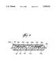
- FIG. 1is an elevational top view of the encapsulated integrated circuit package of the present invention
- FIG. 2is a cross-sectional view taken along the line 2--2 of FIG. 1, and
- FIG. 3is an enlarged fragmentary cross-sectional view taken of the insert 3 of FIG. 2, and
- FIG. 4is a cross-sectional view of another encapsulated integrated circuit package of the present invention.
- the encapsulated integrated circuit package of the present inventionmay take various forms the simplest contains a single integrated circuit die or chip. However the present package is useful for single and multi-chip modules, and for purpose of illustration only will be described in combination with a plurality of integrated circuit chips positioned on one side of a support or substrate.
- the reference numeral 10generally indicates the encapsulated integrated circuit package of the present invention and generally includes one or more integrated circuit dice or chips, here shown as four, being numbers 12, 14, 16, and 18, a housing 20, single or multiple wire screen meshes generally indicated by the reference numeral 22, and a support or substrate 24.
- Electrodes 26extend out of the housing 20.
- Leads 26are integral to a general purpose lead frame and are indirectly connected to chips 12, 14, 16 and 18, for instance by tape-automated-bonded (TAB) leads or wire bonds (not shown). Alternatively, leads 26 could be directly connected to the chips. Whichever the case, leads 26 must be in electrical communication with the chips.
- the substrate 24may also include a heat spreader 28 such as a metal copper heat spreader.
- the housing 20is a non-electrically conductive thermosetting or thermoplastic material which sealingly encloses the substrate 24 and heat spreader 28 as well as the integrated circuit chips 12, 14, 16 and 18.
- the thermoplastic materialmay be of any suitable material, such as polyphenylene sulfide, polyetherimide, polyethersulfone, liquid crystal polymers, or polyetheretherketone.
- suitable thermosetting materialsinclude epoxies such as anhydride epoxy, novalak epoxy, polyimide epoxy and the like.
- Plasticis generally the preferred housing material.
- the wire screen mesh 22comprises at least one thermally conductive screen mesh positioned near or adjacent to the chip or chips 12, 14, 16 and 18 and, preferably, comprises a plurality of flexible layers of screen mesh shown here as layers 30, 32, and 34.
- one of the layers such as 30is exposed to the outside of the housing 20 and thus provides a direct high conductivity path to the outside surface of the package while the other layers are enclosed in the housing and at least one layer, such as layer 34, conforms to the top surfaces of the chips.
- one or more fastenerssuch as hollow or solid stand-offs 36 are stacked or riveted to the substrate 24 and to the corners of the wire screen mesh 22 for securing the mesh 22 to the substrate 24.
- the wire screen meshmay be of any suitable thermally conductive material the materials of copper, aluminum and graphite are most satisfactory.
- the wire screen mesh 22has several important advantages over a conventional solid metal block slug. First, its thermal performance is very comparable to a solid slug as a plurality of screens can provide a comparable volume of thermally conductive material. In addition, and more importantly, the wire screen mesh 22 reduces the thermo-mechanical stress problems that occur with solid slugs of metal. Due to the smaller sizes of the individual strands of the screen mesh the thermo-mechanical stresses created due to the differences in the coefficient of thermal expansion between the housing 20 and the wire screen mesh 22 are minimized. Thirdly, the flexibility of the wire screen mesh 22 allows it to be conformed to and cool an integrated circuit chip structure which has an uneven top surface. As an example only, the individual screens 30, 32 and 34 may have wires 4.5 mils thick with 5.5 mil spacings therebetween to form a mesh with 100 wires per inch. Fourthly, wire screen mesh 22 provides a high degree of RF shielding for the chips.
- package 10aencapsulates chips 14a and 18a which are supported by substrate 24a and connected to leads 26a by wire bonds 38.
- Screen mesh layers 30a, 32a and 34aare positioned adjacent to but spaced from the chips to prevent them from contacting and short-circuiting wire bonds 36.
- a second screen meshcomprising layers 40, 42 and 44 (similar to 30a, 32a and 34a, respectively) is positioned adjacent to substrate 24a on the side opposite chips 14a and 18a to further enhance the package's thermal conductivity.
- second screen mesh layers 40, 42 and 44may be utilized with or without including screen mesh layers 30a, 32a and 34a on the opposite side of substrate 24a.
Landscapes
- Engineering & Computer Science (AREA)
- Physics & Mathematics (AREA)
- Power Engineering (AREA)
- General Physics & Mathematics (AREA)
- Computer Hardware Design (AREA)
- Microelectronics & Electronic Packaging (AREA)
- Condensed Matter Physics & Semiconductors (AREA)
- Health & Medical Sciences (AREA)
- Electromagnetism (AREA)
- Toxicology (AREA)
- Chemical & Material Sciences (AREA)
- Materials Engineering (AREA)
- Cooling Or The Like Of Semiconductors Or Solid State Devices (AREA)
Abstract
Description
Claims (31)
Priority Applications (1)
| Application Number | Priority Date | Filing Date | Title |
|---|---|---|---|
| US07/949,300US5309321A (en) | 1992-09-22 | 1992-09-22 | Thermally conductive screen mesh for encapsulated integrated circuit packages |
Applications Claiming Priority (1)
| Application Number | Priority Date | Filing Date | Title |
|---|---|---|---|
| US07/949,300US5309321A (en) | 1992-09-22 | 1992-09-22 | Thermally conductive screen mesh for encapsulated integrated circuit packages |
Publications (1)
| Publication Number | Publication Date |
|---|---|
| US5309321Atrue US5309321A (en) | 1994-05-03 |
Family
ID=25488874
Family Applications (1)
| Application Number | Title | Priority Date | Filing Date |
|---|---|---|---|
| US07/949,300Expired - LifetimeUS5309321A (en) | 1992-09-22 | 1992-09-22 | Thermally conductive screen mesh for encapsulated integrated circuit packages |
Country Status (1)
| Country | Link |
|---|---|
| US (1) | US5309321A (en) |
Cited By (27)
| Publication number | Priority date | Publication date | Assignee | Title |
|---|---|---|---|---|
| US5545942A (en)* | 1994-11-21 | 1996-08-13 | General Electric Company | Method and apparatus for dissipating heat from a transducer element array of an ultrasound probe |
| US5653280A (en)* | 1995-11-06 | 1997-08-05 | Ncr Corporation | Heat sink assembly and method of affixing the same to electronic devices |
| US5659203A (en)* | 1995-06-07 | 1997-08-19 | International Business Machines Corporation | Reworkable polymer chip encapsulant |
| US5694300A (en)* | 1996-04-01 | 1997-12-02 | Northrop Grumman Corporation | Electromagnetically channelized microwave integrated circuit |
| US6054766A (en)* | 1997-03-06 | 2000-04-25 | Alcatel | Package for enclosing microoptical and/or microelectronic devices so as to minimize the leakage of microwave electromagnetic radiation |
| US6054647A (en)* | 1997-11-26 | 2000-04-25 | National-Standard Company | Grid material for electromagnetic shielding |
| EP1028339A3 (en)* | 1999-02-09 | 2002-01-23 | Sumitomo Electric Industries, Ltd. | Light transmitting/receiving module |
| US6512295B2 (en)* | 2001-03-01 | 2003-01-28 | International Business Machines Corporation | Coupled-cap flip chip BGA package with improved cap design for reduced interfacial stresses |
| US6514616B1 (en) | 1998-07-08 | 2003-02-04 | Queen Mary And Westfield College, University Of London | Thermal management device and method of making such a device |
| US6614102B1 (en) | 2001-05-04 | 2003-09-02 | Amkor Technology, Inc. | Shielded semiconductor leadframe package |
| US6707168B1 (en) | 2001-05-04 | 2004-03-16 | Amkor Technology, Inc. | Shielded semiconductor package with single-sided substrate and method for making the same |
| US20040080915A1 (en)* | 2002-10-24 | 2004-04-29 | Koninklijke Philips Electronics N.V. | Thermal-conductive substrate package |
| US6757181B1 (en)* | 2000-08-22 | 2004-06-29 | Skyworks Solutions, Inc. | Molded shield structures and method for their fabrication |
| WO2005010989A1 (en)* | 2003-07-30 | 2005-02-03 | Koninklijke Philips Electronics, N.V. | Ground arch for wirebond ball grid arrays |
| US20050041394A1 (en)* | 2003-08-22 | 2005-02-24 | Liang Chen Jiunn | Heatsink device |
| EP1608026A2 (en)* | 2004-06-18 | 2005-12-21 | Infineon Technologies Fiber Optics GmbH | Optoelectronic device and method to manufacture the same |
| US20070090519A1 (en)* | 2003-05-01 | 2007-04-26 | Carter Antony A | Encased thermal management device and method of making such a device |
| US7756896B1 (en) | 2002-03-11 | 2010-07-13 | Jp Morgan Chase Bank | System and method for multi-dimensional risk analysis |
| US7890343B1 (en)* | 2005-01-11 | 2011-02-15 | Jp Morgan Chase Bank | System and method for generating risk management curves |
| CN103811472A (en)* | 2012-11-05 | 2014-05-21 | 三星电子株式会社 | Semiconductor package and manufacturing method thereof |
| US9871016B2 (en) | 2015-07-29 | 2018-01-16 | Samsung Electronics Co., Ltd. | Semiconductor package |
| WO2018152378A1 (en)* | 2017-02-15 | 2018-08-23 | Texas Instruments Incorporated | Semiconductor package with a wire bond mesh |
| DE102014112330B4 (en)* | 2013-08-28 | 2020-07-09 | Infineon Technologies Ag | Overmolded substrate-chip arrangement with heat sink, motor control module and associated manufacturing process |
| US10842043B1 (en) | 2019-11-11 | 2020-11-17 | International Business Machines Corporation | Fabricating coolant-cooled heat sinks with internal thermally-conductive fins |
| US11156409B2 (en) | 2020-01-20 | 2021-10-26 | International Business Machines Corporation | Coolant-cooled heat sinks with internal thermally-conductive fins joined to the cover |
| EP4181194A4 (en)* | 2020-09-25 | 2024-03-27 | Honor Device Co., Ltd. | Packaging body and preparation method therefor, terminal and electronic device |
| DE102023204910A1 (en)* | 2023-05-25 | 2024-11-28 | Volkswagen Aktiengesellschaft | Method for producing a power electronic device and use of such a device in a motor vehicle |
Citations (38)
| Publication number | Priority date | Publication date | Assignee | Title |
|---|---|---|---|---|
| US3694699A (en)* | 1970-03-30 | 1972-09-26 | Nat Beryllia Corp | Ceramic based substrates for electronic circuits with improved heat dissipating properties and circuits including the same |
| US4009752A (en)* | 1975-02-24 | 1977-03-01 | Honeywell Information Systems Inc. | Warp-resistant heat sink |
| US4244098A (en)* | 1978-05-26 | 1981-01-13 | General Electric Company | Method of assembling a dynamoelectric machine and an auxiliary cooling device |
| US4333102A (en)* | 1978-12-22 | 1982-06-01 | Bbc Brown, Boveri & Company, Limited | High performance semiconductor component with heat dissipating discs connected by brushlike bundles of wires |
| US4356864A (en)* | 1980-10-08 | 1982-11-02 | Clarion Co., Ltd. | Radiating device for power amplifier etc. |
| US4407006A (en)* | 1979-09-13 | 1983-09-27 | Bbc Brown, Boveri & Company Limited | Spiral strip brushlike stress buffering power semiconductor contacts |
| US4421161A (en)* | 1982-05-06 | 1983-12-20 | Burroughs Corporation | Heat exchanger for integrated circuit packages |
| US4465130A (en)* | 1982-07-06 | 1984-08-14 | Burroughs Corporation | Wire form heat exchange element |
| US4541004A (en)* | 1982-11-24 | 1985-09-10 | Burroughs Corporation | Aerodynamically enhanced heat sink |
| US4598308A (en)* | 1984-04-02 | 1986-07-01 | Burroughs Corporation | Easily repairable, low cost, high speed electromechanical assembly of integrated circuit die |
| US4611238A (en)* | 1982-05-05 | 1986-09-09 | Burroughs Corporation | Integrated circuit package incorporating low-stress omnidirectional heat sink |
| US4620216A (en)* | 1983-04-29 | 1986-10-28 | International Business Machines Corporation | Unitary slotted heat sink for semiconductor packages |
| US4624302A (en)* | 1984-07-02 | 1986-11-25 | At&T Technologies, Inc. | Apparatus for preheating printed circuit boards |
| JPS6281735A (en)* | 1985-10-04 | 1987-04-15 | Sumitomo Electric Ind Ltd | Package with integrated heat dissipation fins |
| US4682208A (en)* | 1984-01-13 | 1987-07-21 | Nissan Motor Co., Ltd. | Transistor protection device |
| US4682651A (en)* | 1986-09-08 | 1987-07-28 | Burroughs Corporation (Now Unisys Corporation) | Segmented heat sink device |
| US4715430A (en)* | 1986-10-27 | 1987-12-29 | International Business Machines Corporation | Environmentally secure and thermally efficient heat sink assembly |
| US4721996A (en)* | 1986-10-14 | 1988-01-26 | Unisys Corporation | Spring loaded module for cooling integrated circuit packages directly with a liquid |
| US4730666A (en)* | 1986-04-30 | 1988-03-15 | International Business Machines Corporation | Flexible finned heat exchanger |
| US4750031A (en)* | 1982-06-25 | 1988-06-07 | The United States Of America As Represented By The United States National Aeronautics And Space Administration | Hermetically sealable package for hybrid solid-state electronic devices and the like |
| US4764804A (en)* | 1986-02-21 | 1988-08-16 | Hitachi, Ltd. | Semiconductor device and process for producing the same |
| US4868349A (en)* | 1988-05-09 | 1989-09-19 | National Semiconductor Corporation | Plastic molded pin-grid-array power package |
| US4878108A (en)* | 1987-06-15 | 1989-10-31 | International Business Machines Corporation | Heat dissipation package for integrated circuits |
| US4888449A (en)* | 1988-01-04 | 1989-12-19 | Olin Corporation | Semiconductor package |
| US4899210A (en)* | 1988-01-20 | 1990-02-06 | Wakefield Engineering, Inc. | Heat sink |
| US4964458A (en)* | 1986-04-30 | 1990-10-23 | International Business Machines Corporation | Flexible finned heat exchanger |
| US4965660A (en)* | 1983-09-22 | 1990-10-23 | Hitachi, Ltd. | Integrated circuit package having heat sink bonded with resinous adhesive |
| US4993482A (en)* | 1990-01-09 | 1991-02-19 | Microelectronics And Computer Technology Corporation | Coiled spring heat transfer element |
| US5006924A (en)* | 1989-12-29 | 1991-04-09 | International Business Machines Corporation | Heat sink for utilization with high density integrated circuit substrates |
| US5022462A (en)* | 1986-04-30 | 1991-06-11 | International Business Machines Corp. | Flexible finned heat exchanger |
| DE4106437A1 (en)* | 1990-02-28 | 1991-08-29 | Hitachi Ltd | DEVICE FOR COOLING LSI CIRCUITS AND DEVICE FOR COOLING A COMPUTER |
| US5057903A (en)* | 1989-07-17 | 1991-10-15 | Microelectronics And Computer Technology Corporation | Thermal heat sink encapsulated integrated circuit |
| US5070936A (en)* | 1991-02-15 | 1991-12-10 | United States Of America As Represented By The Secretary Of The Air Force | High intensity heat exchanger system |
| US5083194A (en)* | 1990-01-16 | 1992-01-21 | Cray Research, Inc. | Air jet impingement on miniature pin-fin heat sinks for cooling electronic components |
| US5146314A (en)* | 1990-03-09 | 1992-09-08 | The University Of Colorado Foundation, Inc. | Apparatus for semiconductor circuit chip cooling using a diamond layer |
| US5155579A (en)* | 1991-02-05 | 1992-10-13 | Advanced Micro Devices | Molded heat sink for integrated circuit package |
| US5156923A (en)* | 1992-01-06 | 1992-10-20 | Texas Instruments Incorporated | Heat-transferring circuit substrate with limited thermal expansion and method for making |
| US5166772A (en)* | 1991-02-22 | 1992-11-24 | Motorola, Inc. | Transfer molded semiconductor device package with integral shield |
- 1992
- 1992-09-22USUS07/949,300patent/US5309321A/ennot_activeExpired - Lifetime
Patent Citations (38)
| Publication number | Priority date | Publication date | Assignee | Title |
|---|---|---|---|---|
| US3694699A (en)* | 1970-03-30 | 1972-09-26 | Nat Beryllia Corp | Ceramic based substrates for electronic circuits with improved heat dissipating properties and circuits including the same |
| US4009752A (en)* | 1975-02-24 | 1977-03-01 | Honeywell Information Systems Inc. | Warp-resistant heat sink |
| US4244098A (en)* | 1978-05-26 | 1981-01-13 | General Electric Company | Method of assembling a dynamoelectric machine and an auxiliary cooling device |
| US4333102A (en)* | 1978-12-22 | 1982-06-01 | Bbc Brown, Boveri & Company, Limited | High performance semiconductor component with heat dissipating discs connected by brushlike bundles of wires |
| US4407006A (en)* | 1979-09-13 | 1983-09-27 | Bbc Brown, Boveri & Company Limited | Spiral strip brushlike stress buffering power semiconductor contacts |
| US4356864A (en)* | 1980-10-08 | 1982-11-02 | Clarion Co., Ltd. | Radiating device for power amplifier etc. |
| US4611238A (en)* | 1982-05-05 | 1986-09-09 | Burroughs Corporation | Integrated circuit package incorporating low-stress omnidirectional heat sink |
| US4421161A (en)* | 1982-05-06 | 1983-12-20 | Burroughs Corporation | Heat exchanger for integrated circuit packages |
| US4750031A (en)* | 1982-06-25 | 1988-06-07 | The United States Of America As Represented By The United States National Aeronautics And Space Administration | Hermetically sealable package for hybrid solid-state electronic devices and the like |
| US4465130A (en)* | 1982-07-06 | 1984-08-14 | Burroughs Corporation | Wire form heat exchange element |
| US4541004A (en)* | 1982-11-24 | 1985-09-10 | Burroughs Corporation | Aerodynamically enhanced heat sink |
| US4620216A (en)* | 1983-04-29 | 1986-10-28 | International Business Machines Corporation | Unitary slotted heat sink for semiconductor packages |
| US4965660A (en)* | 1983-09-22 | 1990-10-23 | Hitachi, Ltd. | Integrated circuit package having heat sink bonded with resinous adhesive |
| US4682208A (en)* | 1984-01-13 | 1987-07-21 | Nissan Motor Co., Ltd. | Transistor protection device |
| US4598308A (en)* | 1984-04-02 | 1986-07-01 | Burroughs Corporation | Easily repairable, low cost, high speed electromechanical assembly of integrated circuit die |
| US4624302A (en)* | 1984-07-02 | 1986-11-25 | At&T Technologies, Inc. | Apparatus for preheating printed circuit boards |
| JPS6281735A (en)* | 1985-10-04 | 1987-04-15 | Sumitomo Electric Ind Ltd | Package with integrated heat dissipation fins |
| US4764804A (en)* | 1986-02-21 | 1988-08-16 | Hitachi, Ltd. | Semiconductor device and process for producing the same |
| US4730666A (en)* | 1986-04-30 | 1988-03-15 | International Business Machines Corporation | Flexible finned heat exchanger |
| US5022462A (en)* | 1986-04-30 | 1991-06-11 | International Business Machines Corp. | Flexible finned heat exchanger |
| US4964458A (en)* | 1986-04-30 | 1990-10-23 | International Business Machines Corporation | Flexible finned heat exchanger |
| US4682651A (en)* | 1986-09-08 | 1987-07-28 | Burroughs Corporation (Now Unisys Corporation) | Segmented heat sink device |
| US4721996A (en)* | 1986-10-14 | 1988-01-26 | Unisys Corporation | Spring loaded module for cooling integrated circuit packages directly with a liquid |
| US4715430A (en)* | 1986-10-27 | 1987-12-29 | International Business Machines Corporation | Environmentally secure and thermally efficient heat sink assembly |
| US4878108A (en)* | 1987-06-15 | 1989-10-31 | International Business Machines Corporation | Heat dissipation package for integrated circuits |
| US4888449A (en)* | 1988-01-04 | 1989-12-19 | Olin Corporation | Semiconductor package |
| US4899210A (en)* | 1988-01-20 | 1990-02-06 | Wakefield Engineering, Inc. | Heat sink |
| US4868349A (en)* | 1988-05-09 | 1989-09-19 | National Semiconductor Corporation | Plastic molded pin-grid-array power package |
| US5057903A (en)* | 1989-07-17 | 1991-10-15 | Microelectronics And Computer Technology Corporation | Thermal heat sink encapsulated integrated circuit |
| US5006924A (en)* | 1989-12-29 | 1991-04-09 | International Business Machines Corporation | Heat sink for utilization with high density integrated circuit substrates |
| US4993482A (en)* | 1990-01-09 | 1991-02-19 | Microelectronics And Computer Technology Corporation | Coiled spring heat transfer element |
| US5083194A (en)* | 1990-01-16 | 1992-01-21 | Cray Research, Inc. | Air jet impingement on miniature pin-fin heat sinks for cooling electronic components |
| DE4106437A1 (en)* | 1990-02-28 | 1991-08-29 | Hitachi Ltd | DEVICE FOR COOLING LSI CIRCUITS AND DEVICE FOR COOLING A COMPUTER |
| US5146314A (en)* | 1990-03-09 | 1992-09-08 | The University Of Colorado Foundation, Inc. | Apparatus for semiconductor circuit chip cooling using a diamond layer |
| US5155579A (en)* | 1991-02-05 | 1992-10-13 | Advanced Micro Devices | Molded heat sink for integrated circuit package |
| US5070936A (en)* | 1991-02-15 | 1991-12-10 | United States Of America As Represented By The Secretary Of The Air Force | High intensity heat exchanger system |
| US5166772A (en)* | 1991-02-22 | 1992-11-24 | Motorola, Inc. | Transfer molded semiconductor device package with integral shield |
| US5156923A (en)* | 1992-01-06 | 1992-10-20 | Texas Instruments Incorporated | Heat-transferring circuit substrate with limited thermal expansion and method for making |
Non-Patent Citations (4)
| Title |
|---|
| "Deltem™ Composite Heat Sinks Introduce A New Dimension to Electronics Heat Transfer", EG&G Wakefield Engineering, Product Brochure, Jun. 1989, pp. 1-4. |
| Deltem Composite Heat Sinks Introduce A New Dimension to Electronics Heat Transfer , EG&G Wakefield Engineering, Product Brochure, Jun. 1989, pp. 1 4.* |
| Dombroski et al, "Thermal Conduction Module", IBM Technical Disclosure Bulletin, vol. 20, No. 6, Nov. 1977, pp. 2214-2215. |
| Dombroski et al, Thermal Conduction Module , IBM Technical Disclosure Bulletin, vol. 20, No. 6, Nov. 1977, pp. 2214 2215.* |
Cited By (37)
| Publication number | Priority date | Publication date | Assignee | Title |
|---|---|---|---|---|
| US5545942A (en)* | 1994-11-21 | 1996-08-13 | General Electric Company | Method and apparatus for dissipating heat from a transducer element array of an ultrasound probe |
| US5659203A (en)* | 1995-06-07 | 1997-08-19 | International Business Machines Corporation | Reworkable polymer chip encapsulant |
| US5930597A (en)* | 1995-06-07 | 1999-07-27 | International Business Machines Corporation | Reworkable polymer chip encapsulant |
| US5653280A (en)* | 1995-11-06 | 1997-08-05 | Ncr Corporation | Heat sink assembly and method of affixing the same to electronic devices |
| US5694300A (en)* | 1996-04-01 | 1997-12-02 | Northrop Grumman Corporation | Electromagnetically channelized microwave integrated circuit |
| US6054766A (en)* | 1997-03-06 | 2000-04-25 | Alcatel | Package for enclosing microoptical and/or microelectronic devices so as to minimize the leakage of microwave electromagnetic radiation |
| US6054647A (en)* | 1997-11-26 | 2000-04-25 | National-Standard Company | Grid material for electromagnetic shielding |
| US6689471B2 (en) | 1998-07-08 | 2004-02-10 | Queen Mary And Westfield College | Thermal management device and method of making such a device |
| US6514616B1 (en) | 1998-07-08 | 2003-02-04 | Queen Mary And Westfield College, University Of London | Thermal management device and method of making such a device |
| EP1028339A3 (en)* | 1999-02-09 | 2002-01-23 | Sumitomo Electric Industries, Ltd. | Light transmitting/receiving module |
| US6757181B1 (en)* | 2000-08-22 | 2004-06-29 | Skyworks Solutions, Inc. | Molded shield structures and method for their fabrication |
| US6512295B2 (en)* | 2001-03-01 | 2003-01-28 | International Business Machines Corporation | Coupled-cap flip chip BGA package with improved cap design for reduced interfacial stresses |
| US6670223B2 (en) | 2001-03-01 | 2003-12-30 | International Business Machines Corporation | Coupled-cap flip chip BGA package with improved cap design for reduced interfacial stresses |
| WO2002071480A3 (en)* | 2001-03-01 | 2003-02-06 | Ibm | Electronic package with improved cap design for reduced interfacial stresses |
| US6614102B1 (en) | 2001-05-04 | 2003-09-02 | Amkor Technology, Inc. | Shielded semiconductor leadframe package |
| US6707168B1 (en) | 2001-05-04 | 2004-03-16 | Amkor Technology, Inc. | Shielded semiconductor package with single-sided substrate and method for making the same |
| US7756896B1 (en) | 2002-03-11 | 2010-07-13 | Jp Morgan Chase Bank | System and method for multi-dimensional risk analysis |
| US6778398B2 (en) | 2002-10-24 | 2004-08-17 | Koninklijke Philips Electronics N.V. | Thermal-conductive substrate package |
| WO2004038795A2 (en) | 2002-10-24 | 2004-05-06 | Koninklijke Philips Electronics N.V. | Thermal-conductive substrate package |
| US20040080915A1 (en)* | 2002-10-24 | 2004-04-29 | Koninklijke Philips Electronics N.V. | Thermal-conductive substrate package |
| US20070090519A1 (en)* | 2003-05-01 | 2007-04-26 | Carter Antony A | Encased thermal management device and method of making such a device |
| WO2005010989A1 (en)* | 2003-07-30 | 2005-02-03 | Koninklijke Philips Electronics, N.V. | Ground arch for wirebond ball grid arrays |
| US20050041394A1 (en)* | 2003-08-22 | 2005-02-24 | Liang Chen Jiunn | Heatsink device |
| US7000683B2 (en)* | 2003-08-22 | 2006-02-21 | Min-Ching Huang | Heatsink device |
| EP1608026A2 (en)* | 2004-06-18 | 2005-12-21 | Infineon Technologies Fiber Optics GmbH | Optoelectronic device and method to manufacture the same |
| US7890343B1 (en)* | 2005-01-11 | 2011-02-15 | Jp Morgan Chase Bank | System and method for generating risk management curves |
| CN103811472A (en)* | 2012-11-05 | 2014-05-21 | 三星电子株式会社 | Semiconductor package and manufacturing method thereof |
| DE102014112330B4 (en)* | 2013-08-28 | 2020-07-09 | Infineon Technologies Ag | Overmolded substrate-chip arrangement with heat sink, motor control module and associated manufacturing process |
| US9871016B2 (en) | 2015-07-29 | 2018-01-16 | Samsung Electronics Co., Ltd. | Semiconductor package |
| WO2018152378A1 (en)* | 2017-02-15 | 2018-08-23 | Texas Instruments Incorporated | Semiconductor package with a wire bond mesh |
| US10204842B2 (en) | 2017-02-15 | 2019-02-12 | Texas Instruments Incorporated | Semiconductor package with a wire bond mesh |
| US11121049B2 (en) | 2017-02-15 | 2021-09-14 | Texas Instruments Incorporated | Semiconductor package with a wire bond mesh |
| US10842043B1 (en) | 2019-11-11 | 2020-11-17 | International Business Machines Corporation | Fabricating coolant-cooled heat sinks with internal thermally-conductive fins |
| US11156409B2 (en) | 2020-01-20 | 2021-10-26 | International Business Machines Corporation | Coolant-cooled heat sinks with internal thermally-conductive fins joined to the cover |
| EP4181194A4 (en)* | 2020-09-25 | 2024-03-27 | Honor Device Co., Ltd. | Packaging body and preparation method therefor, terminal and electronic device |
| US12317464B2 (en) | 2020-09-25 | 2025-05-27 | Honor Device Co., Ltd. | Package body, preparation method thereof, terminal, and electronic device |
| DE102023204910A1 (en)* | 2023-05-25 | 2024-11-28 | Volkswagen Aktiengesellschaft | Method for producing a power electronic device and use of such a device in a motor vehicle |
Similar Documents
| Publication | Publication Date | Title |
|---|---|---|
| US5309321A (en) | Thermally conductive screen mesh for encapsulated integrated circuit packages | |
| US5155579A (en) | Molded heat sink for integrated circuit package | |
| US5254500A (en) | Method for making an integrally molded semiconductor device heat sink | |
| US5598031A (en) | Electrically and thermally enhanced package using a separate silicon substrate | |
| US5399903A (en) | Semiconductor device having an universal die size inner lead layout | |
| US5065281A (en) | Molded integrated circuit package incorporating heat sink | |
| USRE42653E1 (en) | Semiconductor package with heat dissipating structure | |
| US5838545A (en) | High performance, low cost multi-chip modle package | |
| US6723582B2 (en) | Method of making a semiconductor package having exposed metal strap | |
| US5705851A (en) | Thermal ball lead integrated package | |
| US5594234A (en) | Downset exposed die mount pad leadframe and package | |
| US5629561A (en) | Semiconductor package with integral heat dissipator | |
| US5646828A (en) | Thin packaging of multi-chip modules with enhanced thermal/power management | |
| US5067005A (en) | Semiconductor device | |
| US5567983A (en) | Semiconductor apparatus capable of cooling a semiconductor element with radiation efficiency | |
| US5525835A (en) | Semiconductor chip module having an electrically insulative thermally conductive thermal dissipator directly in contact with the semiconductor element | |
| US5168345A (en) | Semiconductor device having a universal die size inner lead layout | |
| US5019893A (en) | Single package, multiple, electrically isolated power semiconductor devices | |
| US3469017A (en) | Encapsulated semiconductor device having internal shielding | |
| EP0533067B1 (en) | Package with heat sink | |
| US20050194698A1 (en) | Integrated circuit package with keep-out zone overlapping undercut zone | |
| JPH06104309A (en) | Semiconductor device | |
| JPH041738Y2 (en) | ||
| JP2814006B2 (en) | Substrate for mounting electronic components | |
| JPS6094746A (en) | Ic mounting method |
Legal Events
| Date | Code | Title | Description |
|---|---|---|---|
| AS | Assignment | Owner name:MICROELECTRONICS AND COMPUTER TECHNOLOGY CORPORATI Free format text:ASSIGNMENT OF ASSIGNORS INTEREST.;ASSIGNORS:OLLA, MICHAEL A.;DOLBEAR, THOMAS P.;HASHEMI, SEYED H.;REEL/FRAME:006278/0257 Effective date:19920915 Owner name:MICROELECTRONICS AND COMPUTER TECHNOLOGY CORPORATI Free format text:ASSIGNMENT OF ASSIGNORS INTEREST;ASSIGNORS:OLLA, MICHAEL A.;DOLBEAR, THOMAS P.;HASHEMI, SEYED H.;REEL/FRAME:006278/0257 Effective date:19920915 | |
| FEPP | Fee payment procedure | Free format text:PAYOR NUMBER ASSIGNED (ORIGINAL EVENT CODE: ASPN); ENTITY STATUS OF PATENT OWNER: LARGE ENTITY | |
| STCF | Information on status: patent grant | Free format text:PATENTED CASE | |
| FPAY | Fee payment | Year of fee payment:4 | |
| REMI | Maintenance fee reminder mailed | ||
| FPAY | Fee payment | Year of fee payment:8 | |
| SULP | Surcharge for late payment | Year of fee payment:7 | |
| AS | Assignment | Owner name:SILICON VALLEY BANK, CALIFORNIA Free format text:SECURITY INTEREST;ASSIGNOR:ROXIO, INC.;REEL/FRAME:015232/0670 Effective date:20040325 Owner name:SILICON VALLEY BANK,CALIFORNIA Free format text:SECURITY INTEREST;ASSIGNOR:ROXIO, INC.;REEL/FRAME:015232/0670 Effective date:20040325 | |
| AS | Assignment | Owner name:STOVOKOR TECHNOLOGY LLC, CALIFORNIA Free format text:ASSIGNMENT OF ASSIGNORS INTEREST;ASSIGNOR:MICROLECTRONICS AND COMPUTER TECHNOLOGY CORPORATION;REEL/FRAME:014892/0165 Effective date:20040128 | |
| FPAY | Fee payment | Year of fee payment:12 | |
| AS | Assignment | Owner name:ROXIO, INC.,CALIFORNIA Free format text:RELEASE BY SECURED PARTY;ASSIGNOR:SILICON VALLEY BANK;REEL/FRAME:018597/0063 Effective date:20061102 Owner name:ROXIO, INC., CALIFORNIA Free format text:RELEASE BY SECURED PARTY;ASSIGNOR:SILICON VALLEY BANK;REEL/FRAME:018597/0063 Effective date:20061102 | |
| FEPP | Fee payment procedure | Free format text:PAYER NUMBER DE-ASSIGNED (ORIGINAL EVENT CODE: RMPN); ENTITY STATUS OF PATENT OWNER: LARGE ENTITY Free format text:PAYOR NUMBER ASSIGNED (ORIGINAL EVENT CODE: ASPN); ENTITY STATUS OF PATENT OWNER: LARGE ENTITY |