US5309063A - Inductive coil for inductively coupled plasma production apparatus - Google Patents
Inductive coil for inductively coupled plasma production apparatusDownload PDFInfo
- Publication number
- US5309063A US5309063AUS08/026,400US2640093AUS5309063AUS 5309063 AUS5309063 AUS 5309063AUS 2640093 AUS2640093 AUS 2640093AUS 5309063 AUS5309063 AUS 5309063A
- Authority
- US
- United States
- Prior art keywords
- coil
- flat
- chamber
- tubular
- window
- Prior art date
- Legal status (The legal status is an assumption and is not a legal conclusion. Google has not performed a legal analysis and makes no representation as to the accuracy of the status listed.)
- Expired - Fee Related
Links
Images


Classifications
- H—ELECTRICITY
- H01—ELECTRIC ELEMENTS
- H01J—ELECTRIC DISCHARGE TUBES OR DISCHARGE LAMPS
- H01J37/00—Discharge tubes with provision for introducing objects or material to be exposed to the discharge, e.g. for the purpose of examination or processing thereof
- H01J37/32—Gas-filled discharge tubes
- H01J37/32009—Arrangements for generation of plasma specially adapted for examination or treatment of objects, e.g. plasma sources
- H01J37/32082—Radio frequency generated discharge
- H01J37/321—Radio frequency generated discharge the radio frequency energy being inductively coupled to the plasma
Definitions
- the inventionrelates to an inductive coil, and, more particularly, to an inductive coil for an inductively coupled plasma production apparatus.
- Plasma systemhave come into use in the processing of semiconductor materials. Inductively coupled system are increasingly being employed for producing the plasma in such systems.
- One type of inductive coil being used in such inductively coupled systemsis a flat or pancake coil such as shown in U.S. Pat. No. 4,948,458.
- the flat coilis mounted externally of the vacuum chamber in which the plasma is generated and is inductively coupled into the plasma through an insulating window.
- this coil configurationhas a number of attractive features, including simplicity of design, it also has a number of limitations.
- One limitationis that it requires an insulating window to allow the RF. field to pass therethrough into the vacuum chamber.
- a second limitationis that the radial plasma density profile, in the plane of the coil, produced by a flat coil is relatively non-uniform.
- the inductive coupling provided by the flat coilhas two components, a capacitive (E) field component and the inductive (H or B) field component. This is undesirable since it is only the inductive component that is desired. Furthermore, with the flat coil, the plasma density drops off rapidly away from the window.
- the inventionis directed to an inductive coil having a planar coil portion and a tubular coil portion extending from the outer edge of the flat coil portion.
- the axis of the tubular coil portionis substantially perpendicular to the flat coil portion.
- the inventionis also directed to a plasma production apparatus which includes a chamber having walls and adapted to be placed under a vacuum.
- An electrodeis in the chamber, and a window extends into the chamber from a wall thereof.
- An induction coilis in the well formed by the window.
- the induction coilhas a flat portion at the bottom of the window and a tubular portion extending from the flat portion.
- FIG. 1is a schematic view of one form of a plasma generating apparatus having the inductive coil of the invention
- FIG. 2is an enlarged view of a portion of the apparatus shown in FIG. 1;
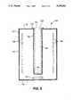
- FIG. 3is a perspective view of a form of the inductive coil of the invention.
- FIG. 4is a graph showing the density of a plasma across a vacuum chamber for a flat coil and the coil of the invention.
- FIG. 5is a schematic view of another form of a plasma generating apparatus having the induction coil of the invention.
- Plasma generating apparatus 10having the inductive coil 12 of the invention.
- Plasma generating apparatus 10comprises a chamber 14 in which there can be generated a vacuum.
- the chamber 14has top and bottom walls 16 and 18, and side walls 20.
- Within the chamber 14 and adjacent the bottom wall 18is an electrode 22.
- the electrode 22is electrically connected to an RF power supply 24 outside the chamber through a matching network circuit 26.
- On the electrode 22is a table 28 for supporting an object, such as a semiconductor wafer, which is to be treated in the plasma.
- the top wall 16has an opening 30 therethrough.
- window 32preferably cup-shaped, extends through the opening 30 and into the chamber 14.
- the window 32has a rim 34 around its upper edge which seats on and is hermetically sealed to the top wall 16 around the opening 30.
- the window 32may be of an insulating material, a conductive material or an insulating material coated on its outer surface with a layer of a conductive material.
- the coil 12is within the well formed by the window 32.
- a pipe 36extends through the bottom wall 18 of the chamber 14 and is connected to means, such as a vacuum pump, for drawing a vacuum in the chamber 14.
- a door 38is in a side wall 20 of the chamber 14 to allow objects to be inserted and removed from the chamber 14.
- An inlet pipe 39extends through a side wall 20 of the chamber 14 to allow for the admission of a plasma forming gas.
- the coil 12is electrically connected to an RF power supply 40 through a matching network circuit 42.
- the RF power supply 40 for the coilmay be the same as or separate from the RF power supply 24 for the electrode 22.
- the coil 12has a flat or pancake portion 44 and a tubular portion 46 extending substantially perpendicularly from the outer edge of the flat portion 44.
- the coil 12is formed of a solid or hollow conductor which is first wound in a spiral to form the flat portion 44 and then wound in the form of a tube to form the tubular portion 46.
- the tubular portion 46may be substantially cylindrical or can be conical. As will be explained, the tubular portion 46 is shaped to provide a desired shape of the plasma formed in the chamber 14.
- a terminal 48is provided at each end of the coil 12 whereby the coil 12 can be connected to the RF power supply 40.
- a coil 12 formed of a hollow conductoris preferred to allow cooling of the coil by flowing a cooling liquid therethrough.
- the dimensions and aspect ratio (the ratio of the size of the flat section 44 to the height of the tubular section 46) of the coil 12can vary depending on the size of the plasma apparatus 10, and in order to shape or modify the plasma profile for a specific purpose.
- a typical coil 12may be formed of 0.6 cm diameter copper tubing with the flat section 44 having between 1 to 3 full turns and an outer diameter of between about 6.3 and 8.9 cm.
- the tubular portion 24is a continuation of the last turn of the flat section 22 and thus has a diameter of between about 6.3 and 8.9 cm.
- the length or height of the tubular portioncan be approximately 8.9 cm.
- an object to be treatedsuch as a semiconductor wafer
- the chamber 14is the evacuated to a desired vacuum.
- a suitable gasis then admitted to the chamber 14.
- the power to the coil 12 and the electrode 22is turned on to create a field across the gas in the chamber 14. This results in the formation of a plasma in the chamber.
- the coil 12 of the inventionhas a number of advantages over the flat coil heretofore used.
- the coil 12has a greater inductive component than the flat coil and therefore generates a greater ion density.
- the coil 12permits a lower pressure of operation than the flat coil.
- the coil 12will produce a more intense plasma for the same RF power resulting in greater gas and electrical (ionization) efficiencies.
- the coil 12provides for greater ease of plasma ignition. Since the coil 12 provides a greater inductive component, the window 32 can be made of a conductive material or of an insulating material coated on its outer surface with a conductive material. A conductive material is less subject to being etched by the plasma in the chamber 14.
- a window formed of a conductive material or having a conductive coating on its outer surface which is subjected to the plasmais less subjected to being etched and therefore has a longer life.
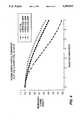
- the most important advantage of the coil 12 of the inventionis that it provides a more uniform plasma density profile across the chamber 14. Referring to FIG. 4, there is shown a graph of the plasma density across one-half of a chamber 14. The distance starts with 0 being directly under the coil. It should be understood that a similar density curve is obtained across the other half of the chamber 14. The curve having the solid dots is for a flat coil. The other three curves are for the coil 14 of the invention (indicated as a hybrid coil) at different power levels. It can be seen from FIG.
- the curves for the coil 14 of the inventionis much flatter than the curve for the flat coil. This shows a more uniform density across the chamber 14.
- the shape of the tubular portion 46 of the coil 14can be varied to alter the plasma density profile.
- the plasma density profilecan be made more uniform by varying the tubular portion 46 between cylindrical and conical.
- Plasma generating apparatus 100comprises a chamber 114 having end walls 116 and 118 and side walls 120. Within the chamber 114 and adjacent an end wall 118 is an electrode 122. The electrode is electrically connected to an RF power supply, not shown, similar to the power supply 24 of FIG. 1.
- An elongated cup-shaped window 132extends through an opening 130 in the end wall 116 and across substantially the full length of the chamber 114.
- the window 132has a rim 134 around its open edge which seats on and is hermetically sealed to the end wall 116.
- the window 132like the window 32 of the apparatus 10 of FIG. 1, may be of an insulating material, a conductive material or an insulating material coated on its outer surface with a layer of a conductive material.
- the coil 112is in the window 132.
- the coil 112like the coil 12, has a flat or pancake portion 144 and a tubular portion 146.
- the only difference between the coil 112 and the coil 12is that the tubular portion 146 of the coil 112 is much longer than the tubular portion 46 of the coil 12.
- the coil 112extends completely along the window 132 with the flat portion 144 being at the closed end of the window 132. This provides the coil 112 along the entire length of the chamber 114.
- the coil 112has terminals which are electrically connected to a RF power supply, such as the power supply 40 of FIG. 1.
- the chamber 114has a pipe which is connected to means, such as a vacuum pump, for drawing a vacuum in the chamber, 114, a door by which articles to be treated can be placed in and removed from the chamber 114, and an inlet pipe to allow for the admission of a plasma forming gas.
- the articles 150 to be treatedsuch as semiconductor wafers, are mounted in the chamber 114 around the window 132. This allows for a larger number of the objects to be treated at one time.
- the apparatus 100operates in the same manner as the apparatus 10 of FIG. 1 except that it permits a greater number of articles to be treated at one time.
- the chamber 114is shown as being vertical, it can also be in a horizontal position.
- an inductive coil 14having a flat portion 44 and a tubular portion 46 extending from the flat portion.
- this coilWhen this coil is used in a plasma generating apparatus 10, it produces greater inductive component than a flat coil and amore uniform plasma density profile across the chamber 14 of the apparatus 10.
- a magnet systemmay be used in the chamber 14 to make the plasma density profile more uniform.
- the coil 14 of the inventiondoes not necessarily need such a magnet.
- the coil 14has been described as being preferably used in a plasma generating apparatus, it can be used in other devices, such as electrodeless high efficient lamps.
Landscapes
- Physics & Mathematics (AREA)
- Engineering & Computer Science (AREA)
- Plasma & Fusion (AREA)
- Chemical & Material Sciences (AREA)
- Analytical Chemistry (AREA)
- Plasma Technology (AREA)
- Chemical Vapour Deposition (AREA)
- Drying Of Semiconductors (AREA)
Abstract
Description
The invention relates to an inductive coil, and, more particularly, to an inductive coil for an inductively coupled plasma production apparatus.
Plasma system have come into use in the processing of semiconductor materials. Inductively coupled system are increasingly being employed for producing the plasma in such systems. One type of inductive coil being used in such inductively coupled systems is a flat or pancake coil such as shown in U.S. Pat. No. 4,948,458. The flat coil is mounted externally of the vacuum chamber in which the plasma is generated and is inductively coupled into the plasma through an insulating window. Although this coil configuration has a number of attractive features, including simplicity of design, it also has a number of limitations. One limitation is that it requires an insulating window to allow the RF. field to pass therethrough into the vacuum chamber. A second limitation is that the radial plasma density profile, in the plane of the coil, produced by a flat coil is relatively non-uniform. Such a window can be expensive to manufacture and is subject to being damaged by the plasma. Also, the inductive coupling provided by the flat coil has two components, a capacitive (E) field component and the inductive (H or B) field component. This is undesirable since it is only the inductive component that is desired. Furthermore, with the flat coil, the plasma density drops off rapidly away from the window.
The invention is directed to an inductive coil having a planar coil portion and a tubular coil portion extending from the outer edge of the flat coil portion. The axis of the tubular coil portion is substantially perpendicular to the flat coil portion.
The invention is also directed to a plasma production apparatus which includes a chamber having walls and adapted to be placed under a vacuum. An electrode is in the chamber, and a window extends into the chamber from a wall thereof. An induction coil is in the well formed by the window. The induction coil has a flat portion at the bottom of the window and a tubular portion extending from the flat portion.
FIG. 1 is a schematic view of one form of a plasma generating apparatus having the inductive coil of the invention;
FIG. 2 is an enlarged view of a portion of the apparatus shown in FIG. 1;
FIG. 3 is a perspective view of a form of the inductive coil of the invention;
FIG. 4 is a graph showing the density of a plasma across a vacuum chamber for a flat coil and the coil of the invention; and
FIG. 5 is a schematic view of another form of a plasma generating apparatus having the induction coil of the invention.
Referring initially to FIG. 1, there is shown aplasma generating apparatus 10 having theinductive coil 12 of the invention.Plasma generating apparatus 10 comprises achamber 14 in which there can be generated a vacuum. Thechamber 14 has top andbottom walls side walls 20. Within thechamber 14 and adjacent thebottom wall 18 is anelectrode 22. Theelectrode 22 is electrically connected to anRF power supply 24 outside the chamber through amatching network circuit 26. On theelectrode 22 is a table 28 for supporting an object, such as a semiconductor wafer, which is to be treated in the plasma. Thetop wall 16 has an opening 30 therethrough. In FIG. 2,window 32, preferably cup-shaped, extends through theopening 30 and into thechamber 14. Thewindow 32 has arim 34 around its upper edge which seats on and is hermetically sealed to thetop wall 16 around the opening 30. Thewindow 32 may be of an insulating material, a conductive material or an insulating material coated on its outer surface with a layer of a conductive material. Thecoil 12 is within the well formed by thewindow 32.
Apipe 36 extends through thebottom wall 18 of thechamber 14 and is connected to means, such as a vacuum pump, for drawing a vacuum in thechamber 14. Adoor 38 is in aside wall 20 of thechamber 14 to allow objects to be inserted and removed from thechamber 14. Aninlet pipe 39 extends through aside wall 20 of thechamber 14 to allow for the admission of a plasma forming gas. Thecoil 12 is electrically connected to anRF power supply 40 through amatching network circuit 42. TheRF power supply 40 for the coil may be the same as or separate from theRF power supply 24 for theelectrode 22.
In FIG. 3, thecoil 12 has a flat orpancake portion 44 and atubular portion 46 extending substantially perpendicularly from the outer edge of theflat portion 44. Thecoil 12 is formed of a solid or hollow conductor which is first wound in a spiral to form theflat portion 44 and then wound in the form of a tube to form thetubular portion 46. Thetubular portion 46 may be substantially cylindrical or can be conical. As will be explained, thetubular portion 46 is shaped to provide a desired shape of the plasma formed in thechamber 14. Aterminal 48 is provided at each end of thecoil 12 whereby thecoil 12 can be connected to theRF power supply 40. Acoil 12 formed of a hollow conductor is preferred to allow cooling of the coil by flowing a cooling liquid therethrough.
The dimensions and aspect ratio (the ratio of the size of theflat section 44 to the height of the tubular section 46) of thecoil 12 can vary depending on the size of theplasma apparatus 10, and in order to shape or modify the plasma profile for a specific purpose. However, for a plasma apparatus which is between about 20 centimeters (cm) and 25 cm in diameter, atypical coil 12 may be formed of 0.6 cm diameter copper tubing with theflat section 44 having between 1 to 3 full turns and an outer diameter of between about 6.3 and 8.9 cm. Thetubular portion 24 is a continuation of the last turn of theflat section 22 and thus has a diameter of between about 6.3 and 8.9 cm. The length or height of the tubular portion can be approximately 8.9 cm.
In the operation of theplasma generating apparatus 10, an object to be treated, such as a semiconductor wafer, is placed in thechamber 14 on the table 28. Thechamber 14 is the evacuated to a desired vacuum. A suitable gas is then admitted to thechamber 14. The power to thecoil 12 and theelectrode 22 is turned on to create a field across the gas in thechamber 14. This results in the formation of a plasma in the chamber.
Thecoil 12 of the invention has a number of advantages over the flat coil heretofore used. Thecoil 12 has a greater inductive component than the flat coil and therefore generates a greater ion density. Thecoil 12 permits a lower pressure of operation than the flat coil. Thecoil 12 will produce a more intense plasma for the same RF power resulting in greater gas and electrical (ionization) efficiencies. Also, thecoil 12 provides for greater ease of plasma ignition. Since thecoil 12 provides a greater inductive component, thewindow 32 can be made of a conductive material or of an insulating material coated on its outer surface with a conductive material. A conductive material is less subject to being etched by the plasma in thechamber 14. Thus, a window formed of a conductive material or having a conductive coating on its outer surface which is subjected to the plasma, is less subjected to being etched and therefore has a longer life. However, the most important advantage of thecoil 12 of the invention is that it provides a more uniform plasma density profile across thechamber 14. Referring to FIG. 4, there is shown a graph of the plasma density across one-half of achamber 14. The distance starts with 0 being directly under the coil. It should be understood that a similar density curve is obtained across the other half of thechamber 14. The curve having the solid dots is for a flat coil. The other three curves are for thecoil 14 of the invention (indicated as a hybrid coil) at different power levels. It can be seen from FIG. 4 that the curves for thecoil 14 of the invention is much flatter than the curve for the flat coil. This shows a more uniform density across thechamber 14. The shape of thetubular portion 46 of thecoil 14 can be varied to alter the plasma density profile. Thus, the plasma density profile can be made more uniform by varying thetubular portion 46 between cylindrical and conical.
In FIG. 5, there is shown another form of aplasma generating apparatus 100 having theinduction coil 112 of the invention.Plasma generating apparatus 100 comprises achamber 114 havingend walls side walls 120. Within thechamber 114 and adjacent anend wall 118 is anelectrode 122. The electrode is electrically connected to an RF power supply, not shown, similar to thepower supply 24 of FIG. 1. An elongated cup-shapedwindow 132 extends through anopening 130 in theend wall 116 and across substantially the full length of thechamber 114. Thewindow 132 has arim 134 around its open edge which seats on and is hermetically sealed to theend wall 116. Thewindow 132, like thewindow 32 of theapparatus 10 of FIG. 1, may be of an insulating material, a conductive material or an insulating material coated on its outer surface with a layer of a conductive material.
Thecoil 112 is in thewindow 132. Thecoil 112, like thecoil 12, has a flat or pancake portion 144 and atubular portion 146. The only difference between thecoil 112 and thecoil 12 is that thetubular portion 146 of thecoil 112 is much longer than thetubular portion 46 of thecoil 12. Thus, thecoil 112 extends completely along thewindow 132 with the flat portion 144 being at the closed end of thewindow 132. This provides thecoil 112 along the entire length of thechamber 114. Although not shown, thecoil 112 has terminals which are electrically connected to a RF power supply, such as thepower supply 40 of FIG. 1.
Although not shown, thechamber 114 has a pipe which is connected to means, such as a vacuum pump, for drawing a vacuum in the chamber, 114, a door by which articles to be treated can be placed in and removed from thechamber 114, and an inlet pipe to allow for the admission of a plasma forming gas. In thechamber 114, thearticles 150 to be treated, such as semiconductor wafers, are mounted in thechamber 114 around thewindow 132. This allows for a larger number of the objects to be treated at one time. Theapparatus 100 operates in the same manner as theapparatus 10 of FIG. 1 except that it permits a greater number of articles to be treated at one time. Although thechamber 114 is shown as being vertical, it can also be in a horizontal position.
Thus, there is provided by the invention aninductive coil 14 having aflat portion 44 and atubular portion 46 extending from the flat portion. When this coil is used in aplasma generating apparatus 10, it produces greater inductive component than a flat coil and amore uniform plasma density profile across thechamber 14 of theapparatus 10. If desired, a magnet system may be used in thechamber 14 to make the plasma density profile more uniform. However, thecoil 14 of the invention does not necessarily need such a magnet. Also, although thecoil 14 has been described as being preferably used in a plasma generating apparatus, it can be used in other devices, such as electrodeless high efficient lamps.
Claims (16)
1. An induction coil comprising a flat coil portion having a plurality of turns and a tubular coil portion extending from the outer edge of the flat coil portion, the axis of the tubular coil portion being substantially perpendicular to the flat coil portion.
2. The coil of claim 1 wherein the coil is of a conductor material wound in a flat spiral to form the flat coil portion and in a tubular spiral to form the tubular coil portion.
3. The coil of claim 2 in which the coil is of a solid conductive material.
4. The coil of claim 2 in which the coil is of a hollow tube.
5. The coil of claim 2 in which the tubular coil portion is cylindrical.
6. The coil of claim 2 in which the tubular coil portion is conical.
7. The coil of claim 2 in which the coil has a pair of ends and terminals are connected to the ends of the coil.
8. A plasma production apparatus comprising:
a chamber having walls and adapted to be placed under a vacuum;
an electrode in the chamber;
a cup-shaped window extending into the chamber through one of the walls; and
an induction coil in the well formed by the window, said coil having a flat coil portion with a plurality of turns at the bottom of the well and a tubular portion extending from the flat portion.
9. The apparatus of claim 8 in which the induction coil is of a conductor material wound in a flat spiral to form the flat portion and then in a tubular spiral to form the tubular portion.
10. The apparatus of claim 9 in which the induction coil is of a solid conductive material.
11. The apparatus of claim 9 in which the induction coil is of a hollow tube.
12. The apparatus of claim 9 in which the tubular portion of the induction coil is cylindrical.
13. The apparatus of claim 9 in which the tubular portion of the induction coil is conical.
14. The apparatus of claim 9 in which the induction coil has a pair of ends and a terminal is attached to each end of the coil.
15. The apparatus of claim 8 in which the window is of a conductive material.
16. The apparatus of claim 8 in which the window is of an insulating material and is coated on its outer surface with a conductive material.
Priority Applications (2)
| Application Number | Priority Date | Filing Date | Title |
|---|---|---|---|
| US08/026,400US5309063A (en) | 1993-03-04 | 1993-03-04 | Inductive coil for inductively coupled plasma production apparatus |
| PCT/US1994/001588WO1994020972A1 (en) | 1993-03-04 | 1994-02-18 | Inductive coil for inductively coupled plasma production apparatus |
Applications Claiming Priority (1)
| Application Number | Priority Date | Filing Date | Title |
|---|---|---|---|
| US08/026,400US5309063A (en) | 1993-03-04 | 1993-03-04 | Inductive coil for inductively coupled plasma production apparatus |
Publications (1)
| Publication Number | Publication Date |
|---|---|
| US5309063Atrue US5309063A (en) | 1994-05-03 |
Family
ID=21831624
Family Applications (1)
| Application Number | Title | Priority Date | Filing Date |
|---|---|---|---|
| US08/026,400Expired - Fee RelatedUS5309063A (en) | 1993-03-04 | 1993-03-04 | Inductive coil for inductively coupled plasma production apparatus |
Country Status (2)
| Country | Link |
|---|---|
| US (1) | US5309063A (en) |
| WO (1) | WO1994020972A1 (en) |
Cited By (50)
| Publication number | Priority date | Publication date | Assignee | Title |
|---|---|---|---|---|
| US5414324A (en)* | 1993-05-28 | 1995-05-09 | The University Of Tennessee Research Corporation | One atmosphere, uniform glow discharge plasma |
| US5430355A (en)* | 1993-07-30 | 1995-07-04 | Texas Instruments Incorporated | RF induction plasma source for plasma processing |
| US5523261A (en)* | 1995-02-28 | 1996-06-04 | Micron Technology, Inc. | Method of cleaning high density inductively coupled plasma chamber using capacitive coupling |
| US5556521A (en)* | 1995-03-24 | 1996-09-17 | Sony Corporation | Sputter etching apparatus with plasma source having a dielectric pocket and contoured plasma source |
| US5589737A (en)* | 1994-12-06 | 1996-12-31 | Lam Research Corporation | Plasma processor for large workpieces |
| US5619103A (en)* | 1993-11-02 | 1997-04-08 | Wisconsin Alumni Research Foundation | Inductively coupled plasma generating devices |
| US5686050A (en)* | 1992-10-09 | 1997-11-11 | The University Of Tennessee Research Corporation | Method and apparatus for the electrostatic charging of a web or film |
| GB2317265A (en)* | 1996-09-13 | 1998-03-18 | Aea Technology Plc | Radio frequency plasma generator |
| EP0838839A3 (en)* | 1996-09-27 | 1998-05-13 | Surface Technology Systems Limited | Plasma processing apparatus |
| US5800619A (en)* | 1996-06-10 | 1998-09-01 | Lam Research Corporation | Vacuum plasma processor having coil with minimum magnetic field in its center |
| US5895558A (en)* | 1995-06-19 | 1999-04-20 | The University Of Tennessee Research Corporation | Discharge methods and electrodes for generating plasmas at one atmosphere of pressure, and materials treated therewith |
| US5938854A (en)* | 1993-05-28 | 1999-08-17 | The University Of Tennessee Research Corporation | Method and apparatus for cleaning surfaces with a glow discharge plasma at one atmosphere of pressure |
| US5955174A (en)* | 1995-03-28 | 1999-09-21 | The University Of Tennessee Research Corporation | Composite of pleated and nonwoven webs |
| US6028395A (en)* | 1997-09-16 | 2000-02-22 | Lam Research Corporation | Vacuum plasma processor having coil with added conducting segments to its peripheral part |
| US6237526B1 (en) | 1999-03-26 | 2001-05-29 | Tokyo Electron Limited | Process apparatus and method for improving plasma distribution and performance in an inductively coupled plasma |
| US6417626B1 (en) | 2001-03-01 | 2002-07-09 | Tokyo Electron Limited | Immersed inductively—coupled plasma source |
| US6474258B2 (en) | 1999-03-26 | 2002-11-05 | Tokyo Electron Limited | Apparatus and method for improving plasma distribution and performance in an inductively coupled plasma |
| US6494998B1 (en) | 2000-08-30 | 2002-12-17 | Tokyo Electron Limited | Process apparatus and method for improving plasma distribution and performance in an inductively coupled plasma using an internal inductive element |
| US6534922B2 (en)* | 1996-09-27 | 2003-03-18 | Surface Technology Systems, Plc | Plasma processing apparatus |
| US6538388B2 (en)* | 2000-10-16 | 2003-03-25 | Alps Electric Co., Ltd. | Plasma processing apparatus suitable for power supply of higher frequency |
| WO2003075965A1 (en)* | 2002-03-08 | 2003-09-18 | Rüdiger Haaga GmbH | Device for sterilizing objects |
| US20040163594A1 (en)* | 2003-02-25 | 2004-08-26 | Tokyo Electron Limited | Method and assembly for providing impedance matching network and network assembly |
| US20040163766A1 (en)* | 2003-02-04 | 2004-08-26 | Veeco Instruments Inc. | Charged particle source and operation thereof |
| US20060028145A1 (en)* | 2004-05-28 | 2006-02-09 | Mohamed Abdel-Aleam H | Method and device for creating a micro plasma jet |
| US20060156983A1 (en)* | 2005-01-19 | 2006-07-20 | Surfx Technologies Llc | Low temperature, atmospheric pressure plasma generation and applications |
| US20080011600A1 (en)* | 2006-07-14 | 2008-01-17 | Makoto Nagashima | Dual hexagonal shaped plasma source |
| US20080014445A1 (en)* | 2004-06-24 | 2008-01-17 | The Regents Of The University Of California | Chamberless Plasma Deposition of Coatings |
| US20080050292A1 (en)* | 2006-08-28 | 2008-02-28 | Valery Godyak | Plasma reactor with inductie excitation of plasma and efficient removal of heat from the excitation coil |
| US20080050537A1 (en)* | 2006-08-22 | 2008-02-28 | Valery Godyak | Inductive plasma source with high coupling efficiency |
| WO2008031321A1 (en)* | 2006-08-23 | 2008-03-20 | Beijing Nmc Co., Ltd. | Inductive coupling coil and inductive coupling plasma apparatus thereof |
| US20090004874A1 (en)* | 2007-06-29 | 2009-01-01 | Lam Research Corporation | Inductively coupled dual zone processing chamber with single planar antenna |
| US20090008239A1 (en)* | 2007-07-06 | 2009-01-08 | Sorensen Carl A | Remote inductively coupled plasma source for cvd chamber cleaning |
| US20090121638A1 (en)* | 2004-05-28 | 2009-05-14 | Price Robert O | Cold air atmospheric pressure micro plasma jet application nethod and device |
| US20100308730A1 (en)* | 2004-05-28 | 2010-12-09 | Mohamed Abdel-Aleam H | Method and device for creating a micro plasma jet |
| US20120031563A1 (en)* | 2009-03-11 | 2012-02-09 | Tokyo Electron Limited | Plasma processing device |
| DE102011013467A1 (en)* | 2011-03-09 | 2012-09-13 | Manz Ag | Apparatus and method for plasma enhanced treatment of at least two substrates |
| US8267884B1 (en) | 2005-10-07 | 2012-09-18 | Surfx Technologies Llc | Wound treatment apparatus and method |
| US8328982B1 (en) | 2005-09-16 | 2012-12-11 | Surfx Technologies Llc | Low-temperature, converging, reactive gas source and method of use |
| US20130059415A1 (en)* | 2011-09-05 | 2013-03-07 | Tokyo Electron Limited | Film deposition apparatus, film deposition method and storage medium |
| US8632651B1 (en) | 2006-06-28 | 2014-01-21 | Surfx Technologies Llc | Plasma surface treatment of composites for bonding |
| US20140150975A1 (en)* | 2010-09-06 | 2014-06-05 | Emd Corporation | Plasma processing device |
| EP2408276A4 (en)* | 2009-03-11 | 2015-10-28 | Emd Corp | Plasma processing apparatus |
| US9406485B1 (en) | 2013-12-18 | 2016-08-02 | Surfx Technologies Llc | Argon and helium plasma apparatus and methods |
| US9583312B2 (en) | 2012-12-14 | 2017-02-28 | Tokyo Electron Limited | Film formation device, substrate processing device, and film formation method |
| US9932674B2 (en) | 2011-05-12 | 2018-04-03 | Tokyo Electron Limited | Film deposition apparatus, film deposition method, and computer-readable recording medium |
| US10032609B1 (en) | 2013-12-18 | 2018-07-24 | Surfx Technologies Llc | Low temperature atmospheric pressure plasma applications |
| US10800092B1 (en) | 2013-12-18 | 2020-10-13 | Surfx Technologies Llc | Low temperature atmospheric pressure plasma for cleaning and activating metals |
| US10827601B1 (en) | 2016-05-03 | 2020-11-03 | Surfx Technologies Llc | Handheld plasma device |
| US20210183619A1 (en)* | 2018-07-26 | 2021-06-17 | Lam Research Corporation | Compact high density plasma source |
| EP3965139A1 (en) | 2020-09-03 | 2022-03-09 | Jozef Stefan Institute | Apparatus, system and method for sustaining inductively coupled plasma |
Citations (13)
| Publication number | Priority date | Publication date | Assignee | Title |
|---|---|---|---|---|
| US2015885A (en)* | 1932-04-22 | 1935-10-01 | Meaf Mach En Apparaten Fab Nv | Method of producing a source of light |
| US3384773A (en)* | 1964-03-12 | 1968-05-21 | Philips Corp | Electric incandescent lamp with levitating incandescent body |
| US3546522A (en)* | 1967-06-21 | 1970-12-08 | Humphreys Corp | Induction plasma generator with gas sheath forming chamber |
| US4206387A (en)* | 1978-09-11 | 1980-06-03 | Gte Laboratories Incorporated | Electrodeless light source having rare earth molecular continua |
| US4836140A (en)* | 1985-12-23 | 1989-06-06 | Hoshin Kagaku Sangyosho Co., Ltd. | Photo-CVD apparatus |
| US4844775A (en)* | 1986-12-11 | 1989-07-04 | Christopher David Dobson | Ion etching and chemical vapour deposition |
| US4894589A (en)* | 1988-08-08 | 1990-01-16 | General Electric Company | Starting means, with piezoelectrically-located capacitive starting electrodes, for HID lamps |
| US4948458A (en)* | 1989-08-14 | 1990-08-14 | Lam Research Corporation | Method and apparatus for producing magnetically-coupled planar plasma |
| US4982140A (en)* | 1989-10-05 | 1991-01-01 | General Electric Company | Starting aid for an electrodeless high intensity discharge lamp |
| US5007373A (en)* | 1989-05-24 | 1991-04-16 | Ionic Atlanta, Inc. | Spiral hollow cathode |
| US5047693A (en)* | 1990-05-23 | 1991-09-10 | General Electric Company | Starting aid for an electrodeless high intensity discharge lamp |
| US5140227A (en)* | 1990-12-04 | 1992-08-18 | General Electric Company | Starting aid for an electrodeless high intensity discharge lamp |
| US5162699A (en)* | 1991-10-11 | 1992-11-10 | Genus, Inc. | Ion source |
- 1993
- 1993-03-04USUS08/026,400patent/US5309063A/ennot_activeExpired - Fee Related
- 1994
- 1994-02-18WOPCT/US1994/001588patent/WO1994020972A1/enactiveApplication Filing
Patent Citations (13)
| Publication number | Priority date | Publication date | Assignee | Title |
|---|---|---|---|---|
| US2015885A (en)* | 1932-04-22 | 1935-10-01 | Meaf Mach En Apparaten Fab Nv | Method of producing a source of light |
| US3384773A (en)* | 1964-03-12 | 1968-05-21 | Philips Corp | Electric incandescent lamp with levitating incandescent body |
| US3546522A (en)* | 1967-06-21 | 1970-12-08 | Humphreys Corp | Induction plasma generator with gas sheath forming chamber |
| US4206387A (en)* | 1978-09-11 | 1980-06-03 | Gte Laboratories Incorporated | Electrodeless light source having rare earth molecular continua |
| US4836140A (en)* | 1985-12-23 | 1989-06-06 | Hoshin Kagaku Sangyosho Co., Ltd. | Photo-CVD apparatus |
| US4844775A (en)* | 1986-12-11 | 1989-07-04 | Christopher David Dobson | Ion etching and chemical vapour deposition |
| US4894589A (en)* | 1988-08-08 | 1990-01-16 | General Electric Company | Starting means, with piezoelectrically-located capacitive starting electrodes, for HID lamps |
| US5007373A (en)* | 1989-05-24 | 1991-04-16 | Ionic Atlanta, Inc. | Spiral hollow cathode |
| US4948458A (en)* | 1989-08-14 | 1990-08-14 | Lam Research Corporation | Method and apparatus for producing magnetically-coupled planar plasma |
| US4982140A (en)* | 1989-10-05 | 1991-01-01 | General Electric Company | Starting aid for an electrodeless high intensity discharge lamp |
| US5047693A (en)* | 1990-05-23 | 1991-09-10 | General Electric Company | Starting aid for an electrodeless high intensity discharge lamp |
| US5140227A (en)* | 1990-12-04 | 1992-08-18 | General Electric Company | Starting aid for an electrodeless high intensity discharge lamp |
| US5162699A (en)* | 1991-10-11 | 1992-11-10 | Genus, Inc. | Ion source |
Cited By (91)
| Publication number | Priority date | Publication date | Assignee | Title |
|---|---|---|---|---|
| US5686050A (en)* | 1992-10-09 | 1997-11-11 | The University Of Tennessee Research Corporation | Method and apparatus for the electrostatic charging of a web or film |
| US5414324A (en)* | 1993-05-28 | 1995-05-09 | The University Of Tennessee Research Corporation | One atmosphere, uniform glow discharge plasma |
| US5938854A (en)* | 1993-05-28 | 1999-08-17 | The University Of Tennessee Research Corporation | Method and apparatus for cleaning surfaces with a glow discharge plasma at one atmosphere of pressure |
| US5430355A (en)* | 1993-07-30 | 1995-07-04 | Texas Instruments Incorporated | RF induction plasma source for plasma processing |
| US5619103A (en)* | 1993-11-02 | 1997-04-08 | Wisconsin Alumni Research Foundation | Inductively coupled plasma generating devices |
| US5589737A (en)* | 1994-12-06 | 1996-12-31 | Lam Research Corporation | Plasma processor for large workpieces |
| US5523261A (en)* | 1995-02-28 | 1996-06-04 | Micron Technology, Inc. | Method of cleaning high density inductively coupled plasma chamber using capacitive coupling |
| US5599396A (en)* | 1995-02-28 | 1997-02-04 | Micron Technology, Inc. | High density inductively and capacitively coupled plasma chamber |
| GB2316530B (en)* | 1995-03-24 | 1998-12-09 | Materials Research Corp | Sputter etching apparatus with plasma source having a dielectric pocket and contoured plasma source |
| US5556521A (en)* | 1995-03-24 | 1996-09-17 | Sony Corporation | Sputter etching apparatus with plasma source having a dielectric pocket and contoured plasma source |
| WO1996030929A1 (en)* | 1995-03-24 | 1996-10-03 | Materials Research Corporation | Sputter etching apparatus with plasma source having a dielectric pocket and contoured plasma source |
| GB2316530A (en)* | 1995-03-24 | 1998-02-25 | Materials Research Corp | Sputter etching apparatus with plasma source having a dielectric pocket and contoured plasma source |
| US5955174A (en)* | 1995-03-28 | 1999-09-21 | The University Of Tennessee Research Corporation | Composite of pleated and nonwoven webs |
| US5895558A (en)* | 1995-06-19 | 1999-04-20 | The University Of Tennessee Research Corporation | Discharge methods and electrodes for generating plasmas at one atmosphere of pressure, and materials treated therewith |
| US6416633B1 (en) | 1995-06-19 | 2002-07-09 | The University Of Tennessee Research Corporation | Resonant excitation method and apparatus for generating plasmas |
| US6059935A (en)* | 1995-06-19 | 2000-05-09 | The University Of Tennessee Research Corporation | Discharge method and apparatus for generating plasmas |
| US5975013A (en)* | 1996-06-10 | 1999-11-02 | Lam Research Corporation | Vacuum plasma processor having coil with small magnetic field in its center |
| US5800619A (en)* | 1996-06-10 | 1998-09-01 | Lam Research Corporation | Vacuum plasma processor having coil with minimum magnetic field in its center |
| WO1998011764A1 (en)* | 1996-09-13 | 1998-03-19 | Aea Technology Plc | Radio frequency plasma generator |
| GB2317265A (en)* | 1996-09-13 | 1998-03-18 | Aea Technology Plc | Radio frequency plasma generator |
| US6534922B2 (en)* | 1996-09-27 | 2003-03-18 | Surface Technology Systems, Plc | Plasma processing apparatus |
| EP0838839A3 (en)* | 1996-09-27 | 1998-05-13 | Surface Technology Systems Limited | Plasma processing apparatus |
| US6259209B1 (en) | 1996-09-27 | 2001-07-10 | Surface Technology Systems Limited | Plasma processing apparatus with coils in dielectric windows |
| KR100505176B1 (en)* | 1996-09-27 | 2005-10-10 | 서페이스 테크놀로지 시스템스 피엘씨 | Plasma Processing Equipment |
| JPH10233297A (en)* | 1996-09-27 | 1998-09-02 | Surface Technol Syst Ltd | Plasma treatment device |
| EP1324371A1 (en)* | 1996-09-27 | 2003-07-02 | Surface Technology Systems Plc | Plasma processing apparatus |
| US6028395A (en)* | 1997-09-16 | 2000-02-22 | Lam Research Corporation | Vacuum plasma processor having coil with added conducting segments to its peripheral part |
| US6474258B2 (en) | 1999-03-26 | 2002-11-05 | Tokyo Electron Limited | Apparatus and method for improving plasma distribution and performance in an inductively coupled plasma |
| US6237526B1 (en) | 1999-03-26 | 2001-05-29 | Tokyo Electron Limited | Process apparatus and method for improving plasma distribution and performance in an inductively coupled plasma |
| US6494998B1 (en) | 2000-08-30 | 2002-12-17 | Tokyo Electron Limited | Process apparatus and method for improving plasma distribution and performance in an inductively coupled plasma using an internal inductive element |
| US6538388B2 (en)* | 2000-10-16 | 2003-03-25 | Alps Electric Co., Ltd. | Plasma processing apparatus suitable for power supply of higher frequency |
| US6417626B1 (en) | 2001-03-01 | 2002-07-09 | Tokyo Electron Limited | Immersed inductively—coupled plasma source |
| CN100584387C (en)* | 2002-03-08 | 2010-01-27 | 鲁迪格哈加有限责任公司 | Item sterilization device |
| WO2003075965A1 (en)* | 2002-03-08 | 2003-09-18 | Rüdiger Haaga GmbH | Device for sterilizing objects |
| US7544334B2 (en) | 2002-03-08 | 2009-06-09 | Ruediger Haaga Gmbh | Device for sterilizing objects |
| GB2401049A (en)* | 2002-03-08 | 2004-11-03 | Haaga Gmbh Rudiger | Device for sterilizing objects |
| GB2401049B (en)* | 2002-03-08 | 2005-08-24 | Haaga Gmbh Rudiger | Arrangement for sterilizing objects |
| US7183716B2 (en)* | 2003-02-04 | 2007-02-27 | Veeco Instruments, Inc. | Charged particle source and operation thereof |
| US20040163766A1 (en)* | 2003-02-04 | 2004-08-26 | Veeco Instruments Inc. | Charged particle source and operation thereof |
| US7212078B2 (en)* | 2003-02-25 | 2007-05-01 | Tokyo Electron Limited | Method and assembly for providing impedance matching network and network assembly |
| US20040163594A1 (en)* | 2003-02-25 | 2004-08-26 | Tokyo Electron Limited | Method and assembly for providing impedance matching network and network assembly |
| US20090121638A1 (en)* | 2004-05-28 | 2009-05-14 | Price Robert O | Cold air atmospheric pressure micro plasma jet application nethod and device |
| US20060028145A1 (en)* | 2004-05-28 | 2006-02-09 | Mohamed Abdel-Aleam H | Method and device for creating a micro plasma jet |
| US20100308730A1 (en)* | 2004-05-28 | 2010-12-09 | Mohamed Abdel-Aleam H | Method and device for creating a micro plasma jet |
| US7572998B2 (en) | 2004-05-28 | 2009-08-11 | Mohamed Abdel-Aleam H | Method and device for creating a micro plasma jet |
| US8502108B2 (en) | 2004-05-28 | 2013-08-06 | Old Dominion University Research Foundation | Method and device for creating a micro plasma jet |
| US8471171B2 (en) | 2004-05-28 | 2013-06-25 | Robert O. Price | Cold air atmospheric pressure micro plasma jet application method and device |
| US20080014445A1 (en)* | 2004-06-24 | 2008-01-17 | The Regents Of The University Of California | Chamberless Plasma Deposition of Coatings |
| US20060156983A1 (en)* | 2005-01-19 | 2006-07-20 | Surfx Technologies Llc | Low temperature, atmospheric pressure plasma generation and applications |
| US8328982B1 (en) | 2005-09-16 | 2012-12-11 | Surfx Technologies Llc | Low-temperature, converging, reactive gas source and method of use |
| US8267884B1 (en) | 2005-10-07 | 2012-09-18 | Surfx Technologies Llc | Wound treatment apparatus and method |
| US8764701B1 (en) | 2005-10-07 | 2014-07-01 | Surfx Technologies Llc | Wound treatment apparatus and method |
| US8632651B1 (en) | 2006-06-28 | 2014-01-21 | Surfx Technologies Llc | Plasma surface treatment of composites for bonding |
| US8454810B2 (en) | 2006-07-14 | 2013-06-04 | 4D-S Pty Ltd. | Dual hexagonal shaped plasma source |
| US20080011600A1 (en)* | 2006-07-14 | 2008-01-17 | Makoto Nagashima | Dual hexagonal shaped plasma source |
| US8444870B2 (en) | 2006-08-22 | 2013-05-21 | Mattson Technology, Inc. | Inductive plasma source with high coupling efficiency |
| US10037867B2 (en) | 2006-08-22 | 2018-07-31 | Mattson Technology, Inc. | Inductive plasma source with high coupling efficiency |
| US8920600B2 (en) | 2006-08-22 | 2014-12-30 | Mattson Technology, Inc. | Inductive plasma source with high coupling efficiency |
| US20080050537A1 (en)* | 2006-08-22 | 2008-02-28 | Valery Godyak | Inductive plasma source with high coupling efficiency |
| US20100136262A1 (en)* | 2006-08-22 | 2010-06-03 | Valery Godyak | Inductive plasma source with high coupling efficiency |
| WO2008031320A1 (en)* | 2006-08-23 | 2008-03-20 | Beijing Nmc Co., Ltd. | Inductive coupling coil and inductive coupling plasma apparatus thereof |
| CN101131893B (en)* | 2006-08-23 | 2011-12-07 | 北京北方微电子基地设备工艺研究中心有限责任公司 | Inductance coupling coil and inductance coupling plasma body device |
| WO2008031321A1 (en)* | 2006-08-23 | 2008-03-20 | Beijing Nmc Co., Ltd. | Inductive coupling coil and inductive coupling plasma apparatus thereof |
| US8992725B2 (en) | 2006-08-28 | 2015-03-31 | Mattson Technology, Inc. | Plasma reactor with inductie excitation of plasma and efficient removal of heat from the excitation coil |
| US20080050292A1 (en)* | 2006-08-28 | 2008-02-28 | Valery Godyak | Plasma reactor with inductie excitation of plasma and efficient removal of heat from the excitation coil |
| US10090134B2 (en) | 2006-08-28 | 2018-10-02 | Mattson Technology, Inc. | Plasma reactor with inductive excitation of plasma and efficient removal of heat from the excitation coil |
| TWI416623B (en)* | 2007-06-29 | 2013-11-21 | Lam Res Corp | Inductively coupled dual zone processing chamber with single planar antenna |
| US20090004874A1 (en)* | 2007-06-29 | 2009-01-01 | Lam Research Corporation | Inductively coupled dual zone processing chamber with single planar antenna |
| US20110230040A1 (en)* | 2007-06-29 | 2011-09-22 | Lam Research Corporation | Inductively coupled dual zone processing chamber with single planar antenna |
| US8119532B2 (en)* | 2007-06-29 | 2012-02-21 | Lam Research Corporation | Inductively coupled dual zone processing chamber with single planar antenna |
| US7972471B2 (en) | 2007-06-29 | 2011-07-05 | Lam Research Corporation | Inductively coupled dual zone processing chamber with single planar antenna |
| US20090008239A1 (en)* | 2007-07-06 | 2009-01-08 | Sorensen Carl A | Remote inductively coupled plasma source for cvd chamber cleaning |
| US8075734B2 (en)* | 2007-07-06 | 2011-12-13 | Applied Materials, Inc. | Remote inductively coupled plasma source for CVD chamber cleaning |
| EP2408276A4 (en)* | 2009-03-11 | 2015-10-28 | Emd Corp | Plasma processing apparatus |
| US20120031563A1 (en)* | 2009-03-11 | 2012-02-09 | Tokyo Electron Limited | Plasma processing device |
| US20140150975A1 (en)* | 2010-09-06 | 2014-06-05 | Emd Corporation | Plasma processing device |
| DE102011013467A8 (en)* | 2011-03-09 | 2012-11-22 | Manz Ag | Apparatus and method for plasma enhanced treatment of at least two substrates |
| DE102011013467A1 (en)* | 2011-03-09 | 2012-09-13 | Manz Ag | Apparatus and method for plasma enhanced treatment of at least two substrates |
| US9932674B2 (en) | 2011-05-12 | 2018-04-03 | Tokyo Electron Limited | Film deposition apparatus, film deposition method, and computer-readable recording medium |
| US9453280B2 (en)* | 2011-09-05 | 2016-09-27 | Tokyo Electron Limited | Film deposition apparatus, film deposition method and storage medium |
| US20130059415A1 (en)* | 2011-09-05 | 2013-03-07 | Tokyo Electron Limited | Film deposition apparatus, film deposition method and storage medium |
| US9583312B2 (en) | 2012-12-14 | 2017-02-28 | Tokyo Electron Limited | Film formation device, substrate processing device, and film formation method |
| US10032609B1 (en) | 2013-12-18 | 2018-07-24 | Surfx Technologies Llc | Low temperature atmospheric pressure plasma applications |
| US9406485B1 (en) | 2013-12-18 | 2016-08-02 | Surfx Technologies Llc | Argon and helium plasma apparatus and methods |
| US10800092B1 (en) | 2013-12-18 | 2020-10-13 | Surfx Technologies Llc | Low temperature atmospheric pressure plasma for cleaning and activating metals |
| US11518082B1 (en) | 2013-12-18 | 2022-12-06 | Surfx Technologies Llc | Low temperature atmospheric pressure plasma for cleaning and activating metals |
| US10827601B1 (en) | 2016-05-03 | 2020-11-03 | Surfx Technologies Llc | Handheld plasma device |
| US12120809B1 (en)* | 2016-05-03 | 2024-10-15 | Surfx Technologies Llc | Handheld plasma device process |
| US20210183619A1 (en)* | 2018-07-26 | 2021-06-17 | Lam Research Corporation | Compact high density plasma source |
| US12198896B2 (en)* | 2018-07-26 | 2025-01-14 | Lam Research Corporation | Compact high density plasma source |
| EP3965139A1 (en) | 2020-09-03 | 2022-03-09 | Jozef Stefan Institute | Apparatus, system and method for sustaining inductively coupled plasma |
Also Published As
| Publication number | Publication date |
|---|---|
| WO1994020972A1 (en) | 1994-09-15 |
Similar Documents
| Publication | Publication Date | Title |
|---|---|---|
| US5309063A (en) | Inductive coil for inductively coupled plasma production apparatus | |
| US6030667A (en) | Apparatus and method for applying RF power apparatus and method for generating plasma and apparatus and method for processing with plasma | |
| US5650032A (en) | Apparatus for producing an inductive plasma for plasma processes | |
| US5210466A (en) | VHF/UHF reactor system | |
| US6251792B1 (en) | Plasma etch processes | |
| US5556501A (en) | Silicon scavenger in an inductively coupled RF plasma reactor | |
| EP0413282B1 (en) | Method and apparatus for producing magnetically-coupled planar plasma | |
| US5767628A (en) | Helicon plasma processing tool utilizing a ferromagnetic induction coil with an internal cooling channel | |
| US5874704A (en) | Low inductance large area coil for an inductively coupled plasma source | |
| US6068784A (en) | Process used in an RF coupled plasma reactor | |
| TWI235404B (en) | Plasma processing apparatus | |
| JP5165821B2 (en) | Multi-coil antenna for inductively coupled plasma generation system | |
| US6518195B1 (en) | Plasma reactor using inductive RF coupling, and processes | |
| US6488807B1 (en) | Magnetic confinement in a plasma reactor having an RF bias electrode | |
| US6444137B1 (en) | Method for processing substrates using gaseous silicon scavenger | |
| US6028285A (en) | High density plasma source for semiconductor processing | |
| EP0553704B1 (en) | Radio frequency induction plasma processing system utilizing a uniform field coil | |
| US5685941A (en) | Inductively coupled plasma reactor with top electrode for enhancing plasma ignition | |
| US20020004309A1 (en) | Processes used in an inductively coupled plasma reactor | |
| US7520246B2 (en) | Power supply antenna and power supply method | |
| TW200405402A (en) | Plasma processing apparatus | |
| CN2726076Y (en) | Inductive comping coil and its inductive coupling plasma apparatus | |
| US20040182319A1 (en) | Inductively coupled plasma generation system with a parallel antenna array having evenly distributed power input and ground nodes | |
| FI117368B (en) | Plasma reactor for a coating or etching process | |
| US6835279B2 (en) | Plasma generation apparatus |
Legal Events
| Date | Code | Title | Description |
|---|---|---|---|
| AS | Assignment | Owner name:DAVID SARNOFF RESEARCH CENTER, INC., NEW JERSEY Free format text:ASSIGNMENT OF ASSIGNORS INTEREST.;ASSIGNOR:SINGH, BAWA;REEL/FRAME:006463/0207 Effective date:19930303 | |
| FPAY | Fee payment | Year of fee payment:4 | |
| AS | Assignment | Owner name:SARNOFF CORPORATION, NEW JERSEY Free format text:MERGER;ASSIGNOR:DAVID SARNOFF RESEARCH CENTER, INC.;REEL/FRAME:009912/0460 Effective date:19970404 | |
| FEPP | Fee payment procedure | Free format text:PAYOR NUMBER ASSIGNED (ORIGINAL EVENT CODE: ASPN); ENTITY STATUS OF PATENT OWNER: LARGE ENTITY | |
| REMI | Maintenance fee reminder mailed | ||
| LAPS | Lapse for failure to pay maintenance fees | ||
| STCH | Information on status: patent discontinuation | Free format text:PATENT EXPIRED DUE TO NONPAYMENT OF MAINTENANCE FEES UNDER 37 CFR 1.362 | |
| FP | Lapsed due to failure to pay maintenance fee | Effective date:20020503 |