US5308783A - Process for the manufacture of a high density cell array of gain memory cells - Google Patents
Process for the manufacture of a high density cell array of gain memory cellsDownload PDFInfo
- Publication number
- US5308783A US5308783AUS07/991,776US99177692AUS5308783AUS 5308783 AUS5308783 AUS 5308783AUS 99177692 AUS99177692 AUS 99177692AUS 5308783 AUS5308783 AUS 5308783A
- Authority
- US
- United States
- Prior art keywords
- layer
- gate
- forming
- depositing
- oxide
- Prior art date
- Legal status (The legal status is an assumption and is not a legal conclusion. Google has not performed a legal analysis and makes no representation as to the accuracy of the status listed.)
- Expired - Lifetime
Links
Images


Classifications
- H—ELECTRICITY
- H10—SEMICONDUCTOR DEVICES; ELECTRIC SOLID-STATE DEVICES NOT OTHERWISE PROVIDED FOR
- H10B—ELECTRONIC MEMORY DEVICES
- H10B12/00—Dynamic random access memory [DRAM] devices
- H10B12/01—Manufacture or treatment
- H—ELECTRICITY
- H10—SEMICONDUCTOR DEVICES; ELECTRIC SOLID-STATE DEVICES NOT OTHERWISE PROVIDED FOR
- H10B—ELECTRONIC MEMORY DEVICES
- H10B12/00—Dynamic random access memory [DRAM] devices
- H10B12/01—Manufacture or treatment
- H10B12/02—Manufacture or treatment for one transistor one-capacitor [1T-1C] memory cells
- H10B12/05—Making the transistor
- H—ELECTRICITY
- H10—SEMICONDUCTOR DEVICES; ELECTRIC SOLID-STATE DEVICES NOT OTHERWISE PROVIDED FOR
- H10B—ELECTRONIC MEMORY DEVICES
- H10B12/00—Dynamic random access memory [DRAM] devices
Definitions
- This inventionrelates to a process for the manufacture of gain memory cells. More particularly, this invention relates to a process for manufacturing a high density cell array of gain memory cells.
- Gain memory cellsare advantageous because they deliver high signal charge, which makes possible very short access times and a simple signal sensing scheme. They comprise a combination of two transistors, an access and a storage transistor, and a diode connecting the source and the gate of the storage transistor.
- Gain memory cellslike other devices for integrated circuits, are subject to increasing miniaturization for VLSI and ULSI circuits, e.g., down to 0.5 micron design rules and smaller.
- the processing needed to manufacture these circuitsmust take into account the minimizing of "real estate" or chip area requirements of the devices, and also the utilization of conventional processing steps and equipment already employed extensively in the semiconductor industry, to minimize the costs of manufacture.
- the process of the inventionprovides for manufacture of high density gain memory cell arrays that feature shallow trench isolation of devices using a planar process, a diode integrated into the gate of the storage transistor, an implanted V DD line to eliminate contact connections of the transistors to the power supply, a buried strap to connect the diode to the source region of the storage transistor and self-aligned device isolation techniques.
- the present processminimizes the cell area requirements of the individual gain memory cells and of the cell array and maximizes cost effectiveness of gain memory cell manufacture using self-aligned process steps and a completely planar process.
- the processcomprises six series of steps; firstly, defining active device regions in a semiconductor substrate, e.g., a silicon wafer, and forming a gate and gate conductor stack; secondly, forming a diode integral with the gate stack; thirdly, defining the gates and ion implanting the source and drain regions of the transistors; fourthly, implanting a V DD line to connect the transistors to the power supply; fifthly, forming a buried strap to connect the diode to the source region of the storage transistor; and finally restructuring the gate, passivating and planarizing the device.
- the process of the inventionuses self-aligning techniques and conventional processing steps to provide an economical process.
- FIGS. 1 to 12are cross sectional views illustrating the structures obtained after various processing steps are performed.
- the present processprovides in a first sequence of steps a planar process for defining active device regions using shallow trench isolation techniques for producing design rules in the 0.5 micron range and smaller.
- This isolation processincludes etching to form shallow trenches, filling in the trenches with nitride and oxide depositions to isolate the device regions, and planarizing the resultant layer.
- Planarizingcan be achieved in any of the subsequently described planarizing steps in known manner by any kind of back etching or by using chemical mechanical polishing as disclosed by Davari et al, IEDM Techn. Dig (1989) p 89. Although illustrated by the shallow trench isolation process, active device regions can also be defined using known LOCOS techniques or channel stopper technologies. This is followed by carrying out a thermal oxide growth to form the transistor gate, and depositing polysilicon thereon as the gate conductor. A silicide layer is formed optimized to minimize sheet resistance of the wordline. The gate stack is formed by the subsequent deposition of nitride and oxide layers.
- the diodeis integrated into the gate stack. Openings are made in the gate stack for the deposition of polysilicon of a dopant type, which is opposite to the dopant type of the polysilicon of the gate conductor, siliciding the polysilicon, filling the openings with oxide and carrying out a planarizing step.
- the first structuring of the gate conductoris carried out by RIE, and a nitride spacer is deposited.
- the source and drain regions of the transistorsare formed by ion implantation.
- an implanted V DD lineis put down to eliminate contacts connecting the storage transistors to the power supply.
- a nitride layeris deposited, openings made in this layer photolithographically, ion implanting the V DD line and siliciding.
- a buried strapis made by depositing a barrier nitride layer, depositing an oxide layer thereon, and planarizing the layers; forming openings in the oxide layer for deposition of polysilicon as the buried strap material, with a final deposition of an oxide layer and planarization thereof.
- a second isolationis carried out, the storage gate is restructured, an oxide fill is used to passivate the device, and a final planarization is carried out.
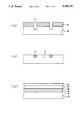
- FIG. 1the surface of a silicon wafer 10 is cleaned in known manner to remove contaminants and particles from the surface.
- photoresist 12is put down over the cleaned silicon wafer and patterned.
- the waferis then etched to form openings 13 therein using standard photo and etch techniques.
- the photoresistis then removed, oxide 14 is deposited (e.g., plasma enhanced CVD oxide or sub atmospheric CVD oxide) and the surface is planarized by etching or chemical mechanical polishing and cleaned.
- FIGS. 3-12do not detail the device isolation in the silicon wafer 10.
- a silicon oxide gate layer 16is thermally grown over the processed silicon wafer 10. For simplicity, this layer 16 is not shown on succeeding figures.
- a gate stackis next formed by sequentially depositing an n-doped polysilicon layer 18, forming a silicide layer 20 thereover, and depositing a nitride layer 22 and an oxide layer 24 over the nitride layer 22.
- the resultant gate stackis shown in FIG. 3.
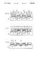
- An integrated diodecomprising a polysilicon layer of one dopant type covered by a polysilicon layer of opposite dopant type is formed in the gate stack by forming an opening 25 by etching through to the silicide layer 20 using photolithographic techniques as shown in FIG. 4. Thereafter a p+ doped polysilicon layer 26 is deposited in the opening.
- This polysilicon layer 26can be deposited as undoped silicon followed by boron-doping by either ion implantation or diffusion techniques.
- the dopant concentrationis chosen so that I(V) characteristics of the polysilicon diode is optimized with respect to the maximum signal charge and to short signal development time.
- This polysilicon depositionis followed by a siliciding step to form a second silicide layer 28. This is shown in FIG. 5.
- an oxide layer 30is deposited (e.g., plasma enhanced CVD oxide or sub-atmospheric CVD oxide) and then the surface of the wafer is planarized by etching or chemical mechanical polishing and cleaned.
- the resultant structureis shown in FIG. 6.
- the gate stacksare now structured by photolithographically patterning the nitride layer 22 and etching through the gate stack comprising the nitride layer 22, the silicide layer 20 and the polysilicon layer 18, the gate oxide layer 16 and the diode portion comprising the filled oxide 30 over the silicide layer 28 and the polysilicon layer 26 using reactive ion etching techniques.
- a spacer nitride layer 32is deposited and etched to form nitride spacers along the sides of the formed gate stack and the planarized diodes. This structure is shown in FIG. 7.
- the transistor source 34 and drain 36 regionsare next ion implanted into the silicon wafer 10. This ion implant is optimized to form dopant levels in the source and drain regions 34, 36 with respect to minimizing cell leakage current.
- the source and drain regionsare thus aligned with the edges of the integrated diode regions, achieving minimum geometric size for the gain memory cells. Further, this allows processing of the diode with a non-critical structure size that is much greater than the minimum geometry size.
- V DD lineis to be made next.
- a nitride barrier layer 38is deposited and patterned to expose the drain region 36 and then a layer of silicide 37 is deposited over the drain region 36. This structure is shown in FIG. 8.
- the dopant concentration of the drain region 36can be increased by ion implantation to achieve a low sheet resistance of the V DD line. This implanted line permits contactless connection of the drains of the storage transistors to the power supply.
- a buried strapis formed next to connect the diode to the source region of the storage transistor using a low resistive material.
- a barrier nitride layer 42is deposited and then a thick oxide layer 44 deposited thereover, see FIG. 9, for planarization and definition of the buried strap using photolithography.
- the thick oxide layer 44is planarized and openings 45 made therein for formation of the buried strap. This structure is shown in FIG. 10.
- a layer of polysilicon 46is deposited into the openings 45 which are then filled with oxide 48.
- the resultant structureis then planarized and is shown in FIG. 11.
- the buried strap to connect the integrated diode to the source region of the storage transistoris a basic feature of the present gain memory cell. Although a particular process using polysilicon has been described for making the buried strap, it will be apparent to those skilled in the art that other processes can be used to connect the diode to the source region of the storage transistor using a low resistance material.
- a second device isolationis carried out by selectively removing oxide except for leaving some oxide over the p-n contact regions and opening recesses 50 and 52 in the oxide layer 44. This can be done in a self-aligned manner using photolithographic patterning and selectively etching the polysilicon down to the oxide which covers the p-n junction. The final self-aligned structure is shown in FIG. 12.
- the cell arrayis completed by structuring the storage transistor gate using a second isolation technique, e.g., a shallow trench isolation process, passivating with an oxide fill and performing a final planarization.
- a second isolation techniquee.g., a shallow trench isolation process
Landscapes
- Engineering & Computer Science (AREA)
- Manufacturing & Machinery (AREA)
- Semiconductor Memories (AREA)
- Metal-Oxide And Bipolar Metal-Oxide Semiconductor Integrated Circuits (AREA)
Abstract
Description
Claims (6)
Priority Applications (7)
| Application Number | Priority Date | Filing Date | Title |
|---|---|---|---|
| US07/991,776US5308783A (en) | 1992-12-16 | 1992-12-16 | Process for the manufacture of a high density cell array of gain memory cells |
| KR1019930025241AKR100308076B1 (en) | 1992-12-16 | 1993-11-25 | How to manufacture a gain memory cell with a high density cell array |
| EP93119790AEP0602525B1 (en) | 1992-12-16 | 1993-12-08 | Process for the manufacture of a high density cell array of gain memory cells |
| AT93119790TATE184424T1 (en) | 1992-12-16 | 1993-12-08 | PRODUCTION METHOD FOR A HIGH DENSITY MEMORY CELL ARRANGEMENT OF THE GAIN CELL TYPE |
| DE69326312TDE69326312T2 (en) | 1992-12-16 | 1993-12-08 | Manufacturing method for a high density memory cell arrangement of the gain cell type |
| JP34132893AJP3495071B2 (en) | 1992-12-16 | 1993-12-10 | Method of manufacturing an array of gain memory cells |
| HK98102937.5AHK1003755B (en) | 1992-12-16 | 1998-04-08 | Process for the manufacture of a high density cell array of gain memory cells |
Applications Claiming Priority (1)
| Application Number | Priority Date | Filing Date | Title |
|---|---|---|---|
| US07/991,776US5308783A (en) | 1992-12-16 | 1992-12-16 | Process for the manufacture of a high density cell array of gain memory cells |
Publications (1)
| Publication Number | Publication Date |
|---|---|
| US5308783Atrue US5308783A (en) | 1994-05-03 |
Family
ID=25537551
Family Applications (1)
| Application Number | Title | Priority Date | Filing Date |
|---|---|---|---|
| US07/991,776Expired - LifetimeUS5308783A (en) | 1992-12-16 | 1992-12-16 | Process for the manufacture of a high density cell array of gain memory cells |
Country Status (6)
| Country | Link |
|---|---|
| US (1) | US5308783A (en) |
| EP (1) | EP0602525B1 (en) |
| JP (1) | JP3495071B2 (en) |
| KR (1) | KR100308076B1 (en) |
| AT (1) | ATE184424T1 (en) |
| DE (1) | DE69326312T2 (en) |
Cited By (17)
| Publication number | Priority date | Publication date | Assignee | Title |
|---|---|---|---|---|
| US5543348A (en)* | 1995-03-29 | 1996-08-06 | Kabushiki Kaisha Toshiba | Controlled recrystallization of buried strap in a semiconductor memory device |
| US5587331A (en)* | 1992-12-19 | 1996-12-24 | Goldstar Electron Co., Ltd. | Method of forming a contact hole for a metal line in a semiconductor device |
| US5677563A (en)* | 1994-05-19 | 1997-10-14 | International Business Machines Corporation | Gate stack structure of a field effect transistor |
| US5732014A (en)* | 1997-02-20 | 1998-03-24 | Micron Technology, Inc. | Merged transistor structure for gain memory cell |
| US5854500A (en)* | 1995-09-26 | 1998-12-29 | Siemens Aktiengesellschaft | DRAM cell array with dynamic gain memory cells |
| US5905279A (en)* | 1996-04-09 | 1999-05-18 | Kabushiki Kaisha Toshiba | Low resistant trench fill for a semiconductor device |
| US6025220A (en)* | 1996-06-18 | 2000-02-15 | Micron Technology, Inc. | Method of forming a polysilicon diode and devices incorporating such diode |
| US6436760B1 (en)* | 2001-04-19 | 2002-08-20 | International Business Machines Corporation | Method for reducing surface oxide in polysilicon processing |
| US20040042256A1 (en)* | 2002-08-29 | 2004-03-04 | Micron Technology, Inc. | Single transistor vertical memory gain cell |
| US20040041236A1 (en)* | 2002-08-29 | 2004-03-04 | Micron Technology, Inc. | Merged mos-bipolar capacitor memory cell |
| US20040061190A1 (en)* | 2002-09-30 | 2004-04-01 | International Business Machines Corporation | Method and structure for tungsten gate metal surface treatment while preventing oxidation |
| US20040108532A1 (en)* | 2002-12-04 | 2004-06-10 | Micron Technology, Inc. | Embedded DRAM gain memory cell |
| US6804142B2 (en) | 2002-11-12 | 2004-10-12 | Micron Technology, Inc. | 6F2 3-transistor DRAM gain cell |
| US20050024936A1 (en)* | 2003-03-04 | 2005-02-03 | Micron Technology, Inc. | Vertical gain cell |
| US6979651B1 (en)* | 2002-07-29 | 2005-12-27 | Advanced Micro Devices, Inc. | Method for forming alignment features and back-side contacts with fewer lithography and etch steps |
| US20080097189A1 (en)* | 2006-09-12 | 2008-04-24 | General Electric Company | Combined MR imaging and tracking |
| US10190390B2 (en) | 2012-10-15 | 2019-01-29 | Baker Hughes, A Ge Company, Llc | Pressure actuated ported sub for subterranean cement completions |
Families Citing this family (1)
| Publication number | Priority date | Publication date | Assignee | Title |
|---|---|---|---|---|
| US20160064285A1 (en)* | 2013-03-27 | 2016-03-03 | Ps4 Luxco S.A.R.L.) | Manufacturing method for semiconductor device |
Citations (7)
| Publication number | Priority date | Publication date | Assignee | Title |
|---|---|---|---|---|
| US4416404A (en)* | 1983-01-26 | 1983-11-22 | Daniels Fitz A S C | Belt type garment for carrying tennis balls and the like |
| US4432073A (en)* | 1980-01-25 | 1984-02-14 | Tokyo Shibaura Denki Kabushiki Kaisha | Semiconductor memory device |
| US4543595A (en)* | 1982-05-20 | 1985-09-24 | Fairchild Camera And Instrument Corporation | Bipolar memory cell |
| US4631705A (en)* | 1983-06-23 | 1986-12-23 | Nec Corporation | Semiconductor integrated circuit memory device |
| US4654825A (en)* | 1984-01-06 | 1987-03-31 | Advanced Micro Devices, Inc. | E2 prom memory cell |
| US4914740A (en)* | 1988-03-07 | 1990-04-03 | International Business Corporation | Charge amplifying trench memory cell |
| US5021849A (en)* | 1989-10-30 | 1991-06-04 | Motorola, Inc. | Compact SRAM cell with polycrystalline silicon diode load |
Family Cites Families (4)
| Publication number | Priority date | Publication date | Assignee | Title |
|---|---|---|---|---|
| CA1322250C (en)* | 1987-08-31 | 1993-09-14 | Loren Thomas Lancaster | Active dynamic memory cell |
| JPH01145850A (en)* | 1987-12-02 | 1989-06-07 | Oki Electric Ind Co Ltd | Semiconductor memory device |
| JPH01255269A (en)* | 1988-04-05 | 1989-10-12 | Oki Electric Ind Co Ltd | semiconductor storage device |
| GB2238427A (en)* | 1989-11-24 | 1991-05-29 | Philips Electronic Associated | Thin film diode devices and active matrix addressed display devices incorporating such |
- 1992
- 1992-12-16USUS07/991,776patent/US5308783A/ennot_activeExpired - Lifetime
- 1993
- 1993-11-25KRKR1019930025241Apatent/KR100308076B1/ennot_activeExpired - Fee Related
- 1993-12-08ATAT93119790Tpatent/ATE184424T1/ennot_activeIP Right Cessation
- 1993-12-08DEDE69326312Tpatent/DE69326312T2/ennot_activeExpired - Fee Related
- 1993-12-08EPEP93119790Apatent/EP0602525B1/ennot_activeExpired - Lifetime
- 1993-12-10JPJP34132893Apatent/JP3495071B2/ennot_activeExpired - Fee Related
Patent Citations (7)
| Publication number | Priority date | Publication date | Assignee | Title |
|---|---|---|---|---|
| US4432073A (en)* | 1980-01-25 | 1984-02-14 | Tokyo Shibaura Denki Kabushiki Kaisha | Semiconductor memory device |
| US4543595A (en)* | 1982-05-20 | 1985-09-24 | Fairchild Camera And Instrument Corporation | Bipolar memory cell |
| US4416404A (en)* | 1983-01-26 | 1983-11-22 | Daniels Fitz A S C | Belt type garment for carrying tennis balls and the like |
| US4631705A (en)* | 1983-06-23 | 1986-12-23 | Nec Corporation | Semiconductor integrated circuit memory device |
| US4654825A (en)* | 1984-01-06 | 1987-03-31 | Advanced Micro Devices, Inc. | E2 prom memory cell |
| US4914740A (en)* | 1988-03-07 | 1990-04-03 | International Business Corporation | Charge amplifying trench memory cell |
| US5021849A (en)* | 1989-10-30 | 1991-06-04 | Motorola, Inc. | Compact SRAM cell with polycrystalline silicon diode load |
Cited By (51)
| Publication number | Priority date | Publication date | Assignee | Title |
|---|---|---|---|---|
| US5587331A (en)* | 1992-12-19 | 1996-12-24 | Goldstar Electron Co., Ltd. | Method of forming a contact hole for a metal line in a semiconductor device |
| US5677563A (en)* | 1994-05-19 | 1997-10-14 | International Business Machines Corporation | Gate stack structure of a field effect transistor |
| US5543348A (en)* | 1995-03-29 | 1996-08-06 | Kabushiki Kaisha Toshiba | Controlled recrystallization of buried strap in a semiconductor memory device |
| US5670805A (en)* | 1995-03-29 | 1997-09-23 | Kabushiki Kaisha Toshiba | Controlled recrystallization of buried strap in a semiconductor memory device |
| US5854500A (en)* | 1995-09-26 | 1998-12-29 | Siemens Aktiengesellschaft | DRAM cell array with dynamic gain memory cells |
| US5905279A (en)* | 1996-04-09 | 1999-05-18 | Kabushiki Kaisha Toshiba | Low resistant trench fill for a semiconductor device |
| US6025220A (en)* | 1996-06-18 | 2000-02-15 | Micron Technology, Inc. | Method of forming a polysilicon diode and devices incorporating such diode |
| US6229157B1 (en) | 1996-06-18 | 2001-05-08 | Micron Technology, Inc. | Method of forming a polysilicon diode and devices incorporating such diode |
| US6392913B1 (en) | 1996-06-18 | 2002-05-21 | Micron Technology, Inc. | Method of forming a polysilicon diode and devices incorporating such diode |
| US5732014A (en)* | 1997-02-20 | 1998-03-24 | Micron Technology, Inc. | Merged transistor structure for gain memory cell |
| US5897351A (en)* | 1997-02-20 | 1999-04-27 | Micron Technology, Inc. | Method for forming merged transistor structure for gain memory cell |
| US6436760B1 (en)* | 2001-04-19 | 2002-08-20 | International Business Machines Corporation | Method for reducing surface oxide in polysilicon processing |
| US6979651B1 (en)* | 2002-07-29 | 2005-12-27 | Advanced Micro Devices, Inc. | Method for forming alignment features and back-side contacts with fewer lithography and etch steps |
| US20050094453A1 (en)* | 2002-08-29 | 2005-05-05 | Micron Technology, Inc. | Merged MOS-bipolar capacitor memory cell |
| US6943083B2 (en) | 2002-08-29 | 2005-09-13 | Micron Technology, Inc. | Merged MOS-bipolar capacitor memory cell |
| US7608876B2 (en) | 2002-08-29 | 2009-10-27 | Micron Technology, Inc. | Merged MOS-bipolar capacitor memory cell |
| US7149109B2 (en) | 2002-08-29 | 2006-12-12 | Micron Technology, Inc. | Single transistor vertical memory gain cell |
| US20060252206A1 (en)* | 2002-08-29 | 2006-11-09 | Micron Technology, Inc. | Single transistor vertical memory gain cell |
| US6838723B2 (en) | 2002-08-29 | 2005-01-04 | Micron Technology, Inc. | Merged MOS-bipolar capacitor memory cell |
| US20060231879A1 (en)* | 2002-08-29 | 2006-10-19 | Micron Technology, Inc. | Merged MOS-bipolar capacitor memory cell |
| US7564087B2 (en) | 2002-08-29 | 2009-07-21 | Micron Technology, Inc. | Merged MOS-bipolar capacitor memory cell |
| US7323380B2 (en) | 2002-08-29 | 2008-01-29 | Micron Technology, Inc. | Single transistor vertical memory gain cell |
| US20050041457A1 (en)* | 2002-08-29 | 2005-02-24 | Micron Technology, Inc. | Single transistor vertical memory gain cell |
| US20050068828A1 (en)* | 2002-08-29 | 2005-03-31 | Micron Technology, Inc. | Merged MOS-bipolar capacitor memory cell |
| US20040041236A1 (en)* | 2002-08-29 | 2004-03-04 | Micron Technology, Inc. | Merged mos-bipolar capacitor memory cell |
| US6940761B2 (en) | 2002-08-29 | 2005-09-06 | Micron Technology, Inc. | Merged MOS-bipolar capacitor memory cell |
| US7199417B2 (en) | 2002-08-29 | 2007-04-03 | Micron Technology, Inc. | Merged MOS-bipolar capacitor memory cell |
| US7224024B2 (en) | 2002-08-29 | 2007-05-29 | Micron Technology, Inc. | Single transistor vertical memory gain cell |
| US20050265069A1 (en)* | 2002-08-29 | 2005-12-01 | Micron Technology, Inc. | Merged mos-bipolar capacitor memory cell |
| US20040042256A1 (en)* | 2002-08-29 | 2004-03-04 | Micron Technology, Inc. | Single transistor vertical memory gain cell |
| US20040061190A1 (en)* | 2002-09-30 | 2004-04-01 | International Business Machines Corporation | Method and structure for tungsten gate metal surface treatment while preventing oxidation |
| US7186633B2 (en) | 2002-09-30 | 2007-03-06 | International Business Machines Corporation | Method and structure for tungsten gate metal surface treatment while preventing oxidation |
| US20040229451A1 (en)* | 2002-09-30 | 2004-11-18 | Haining Yang | Method and structure for tungsten gate metal surface treatment while preventing oxidation |
| US6975531B2 (en) | 2002-11-12 | 2005-12-13 | Micron Technology, Inc. | 6F2 3-transistor DRAM gain cell |
| US20060028859A1 (en)* | 2002-11-12 | 2006-02-09 | Micron Technology, Inc. | 6F2 3-Transistor DRAM gain cell |
| US20050012130A1 (en)* | 2002-11-12 | 2005-01-20 | Micron Technology, Inc. | 6F2 3-Transistor DRAM gain cell |
| US6804142B2 (en) | 2002-11-12 | 2004-10-12 | Micron Technology, Inc. | 6F2 3-transistor DRAM gain cell |
| US7151690B2 (en) | 2002-11-12 | 2006-12-19 | Micron Technology, Inc. | 6F2 3-Transistor DRAM gain cell |
| US7030436B2 (en) | 2002-12-04 | 2006-04-18 | Micron Technology, Inc. | Embedded DRAM gain memory cell having MOS transistor body provided with a bi-polar transistor charge injecting means |
| US20060181919A1 (en)* | 2002-12-04 | 2006-08-17 | Micron Technology, Inc. | Embedded DRAM gain memory cell |
| US20040108532A1 (en)* | 2002-12-04 | 2004-06-10 | Micron Technology, Inc. | Embedded DRAM gain memory cell |
| US6956256B2 (en) | 2003-03-04 | 2005-10-18 | Micron Technology Inc. | Vertical gain cell |
| US7241658B2 (en) | 2003-03-04 | 2007-07-10 | Micron Technology, Inc. | Vertical gain cell |
| US20070158722A1 (en)* | 2003-03-04 | 2007-07-12 | Micron Technology, Inc. | Vertical gain cell |
| US7298638B2 (en) | 2003-03-04 | 2007-11-20 | Micron Technology, Inc. | Operating an electronic device having a vertical gain cell that includes vertical MOS transistors |
| US20050032313A1 (en)* | 2003-03-04 | 2005-02-10 | Micron Technology, Inc. | Vertical gain cell |
| US7528440B2 (en) | 2003-03-04 | 2009-05-05 | Micron Technology, Inc. | Vertical gain cell |
| US20050024936A1 (en)* | 2003-03-04 | 2005-02-03 | Micron Technology, Inc. | Vertical gain cell |
| US20080097189A1 (en)* | 2006-09-12 | 2008-04-24 | General Electric Company | Combined MR imaging and tracking |
| US8583213B2 (en) | 2006-09-12 | 2013-11-12 | General Electric Company | Combined MR imaging and tracking |
| US10190390B2 (en) | 2012-10-15 | 2019-01-29 | Baker Hughes, A Ge Company, Llc | Pressure actuated ported sub for subterranean cement completions |
Also Published As
| Publication number | Publication date |
|---|---|
| KR940016777A (en) | 1994-07-25 |
| JP3495071B2 (en) | 2004-02-09 |
| ATE184424T1 (en) | 1999-09-15 |
| HK1003755A1 (en) | 1998-11-06 |
| EP0602525B1 (en) | 1999-09-08 |
| DE69326312D1 (en) | 1999-10-14 |
| KR100308076B1 (en) | 2001-12-15 |
| DE69326312T2 (en) | 2000-02-17 |
| JPH06216330A (en) | 1994-08-05 |
| EP0602525A1 (en) | 1994-06-22 |
Similar Documents
| Publication | Publication Date | Title |
|---|---|---|
| US5308783A (en) | Process for the manufacture of a high density cell array of gain memory cells | |
| US6767789B1 (en) | Method for interconnection between transfer devices and storage capacitors in memory cells and device formed thereby | |
| US5306935A (en) | Method of forming a nonvolatile stacked memory | |
| US5292677A (en) | Reduced mask CMOS process for fabricating stacked capacitor multi-megabit dynamic random access memories utilizing single etch stop layer for contacts | |
| US5627393A (en) | Vertical channel device having buried source | |
| US6395597B2 (en) | Trench DRAM cell with vertical device and buried word lines | |
| US6204112B1 (en) | Process for forming a high density semiconductor device | |
| US5482883A (en) | Method for fabricating low leakage substrate plate trench DRAM cells and devices formed thereby | |
| US5324960A (en) | Dual-transistor structure and method of formation | |
| US5716881A (en) | Process to fabricate stacked capacitor DRAM and low power thin film transistor SRAM devices on a single semiconductor chip | |
| US4656731A (en) | Method for fabricating stacked CMOS transistors with a self-aligned silicide process | |
| US5324973A (en) | Semiconductor SRAM with trench transistors | |
| US5510287A (en) | Method of making vertical channel mask ROM | |
| US5675176A (en) | Semiconductor device and a method for manufacturing the same | |
| US6312982B1 (en) | Method of fabricating a trench capacitor | |
| US5027172A (en) | Dynamic random access memory cell and method of making thereof | |
| US6444520B1 (en) | Method of forming dual conductive plugs | |
| US20060134898A1 (en) | Semiconductor damascene trench and methods thereof | |
| US6096644A (en) | Self-aligned contacts to source/drain silicon electrodes utilizing polysilicon and metal silicides | |
| US6566200B2 (en) | Flash memory array structure and method of forming | |
| JPH0691210B2 (en) | High performance trench capacitor for DRAM cell | |
| US6319840B1 (en) | For mol integration | |
| EP0513532B1 (en) | Trench DRAM cell with substrate plate | |
| HK1003755B (en) | Process for the manufacture of a high density cell array of gain memory cells | |
| US6117754A (en) | Trench free process for SRAM with buried contact structure |
Legal Events
| Date | Code | Title | Description |
|---|---|---|---|
| AS | Assignment | Owner name:SIEMENS COMPONENTS, INC., NEW JERSEY Free format text:ASSIGNMENT OF ASSIGNORS INTEREST.;ASSIGNOR:KLINGENSTEIN, WERNER M.;REEL/FRAME:006479/0078 Effective date:19930318 Owner name:SIEMENS COMPONENTS, INC., NEW JERSEY Free format text:ASSIGNMENT OF ASSIGNORS INTEREST.;ASSIGNOR:KRAUTSCHNEIDER, WOLFGANG H.;REEL/FRAME:006466/0985 Effective date:19930322 | |
| AS | Assignment | Owner name:SIEMENS AKTIENGESELLSCHAFT, GERMANY Free format text:ASSIGNMENT OF ASSIGNORS INTEREST;ASSIGNOR:SIEMENS COMPONENTS, INC.;REEL/FRAME:006752/0406 Effective date:19931008 | |
| STCF | Information on status: patent grant | Free format text:PATENTED CASE | |
| FEPP | Fee payment procedure | Free format text:PAYOR NUMBER ASSIGNED (ORIGINAL EVENT CODE: ASPN); ENTITY STATUS OF PATENT OWNER: LARGE ENTITY | |
| FPAY | Fee payment | Year of fee payment:4 | |
| FPAY | Fee payment | Year of fee payment:8 | |
| FEPP | Fee payment procedure | Free format text:PAYOR NUMBER ASSIGNED (ORIGINAL EVENT CODE: ASPN); ENTITY STATUS OF PATENT OWNER: LARGE ENTITY Free format text:PAYER NUMBER DE-ASSIGNED (ORIGINAL EVENT CODE: RMPN); ENTITY STATUS OF PATENT OWNER: LARGE ENTITY | |
| REMI | Maintenance fee reminder mailed | ||
| FPAY | Fee payment | Year of fee payment:12 | |
| SULP | Surcharge for late payment | Year of fee payment:11 | |
| AS | Assignment | Owner name:INFINEON TECHNOLOGIES AG, GERMANY Free format text:ASSIGNMENT OF ASSIGNORS INTEREST;ASSIGNOR:SIEMENS AKTIENGESELLSCHAFT;REEL/FRAME:017718/0394 Effective date:20060522 | |
| AS | Assignment | Owner name:QIMONDA AG, GERMANY Free format text:ASSIGNMENT OF ASSIGNORS INTEREST;ASSIGNOR:INFINEON TECHNOLOGIES AG;REEL/FRAME:023519/0078 Effective date:20060905 Owner name:MOSAID TECHNOLOGIES INCORPORATED, CANADA Free format text:ASSIGNMENT OF ASSIGNORS INTEREST;ASSIGNOR:QIMONDA AG;REEL/FRAME:023519/0083 Effective date:20060905 Owner name:MOSAID TECHNOLOGIES INCORPORATED, CANADA Free format text:ASSIGNMENT OF ASSIGNORS INTEREST;ASSIGNOR:MOSAID TECHNOLOGIES INCORPORATED;REEL/FRAME:023519/0090 Effective date:20090209 | |
| AS | Assignment | Owner name:ROYAL BANK OF CANADA, CANADA Free format text:U.S. INTELLECTUAL PROPERTY SECURITY AGREEMENT (FOR NON-U.S. GRANTORS) - SHORT FORM;ASSIGNORS:658276 N.B. LTD.;658868 N.B. INC.;MOSAID TECHNOLOGIES INCORPORATED;REEL/FRAME:027512/0196 Effective date:20111223 |