US5306923A - Optoelectric device with a very low series resistance - Google Patents
Optoelectric device with a very low series resistanceDownload PDFInfo
- Publication number
- US5306923A US5306923AUS07/980,263US98026392AUS5306923AUS 5306923 AUS5306923 AUS 5306923AUS 98026392 AUS98026392 AUS 98026392AUS 5306923 AUS5306923 AUS 5306923A
- Authority
- US
- United States
- Prior art keywords
- layer
- doped
- active
- confinement layer
- confinement
- Prior art date
- Legal status (The legal status is an assumption and is not a legal conclusion. Google has not performed a legal analysis and makes no representation as to the accuracy of the status listed.)
- Expired - Lifetime
Links
Images

Classifications
- H—ELECTRICITY
- H01—ELECTRIC ELEMENTS
- H01S—DEVICES USING THE PROCESS OF LIGHT AMPLIFICATION BY STIMULATED EMISSION OF RADIATION [LASER] TO AMPLIFY OR GENERATE LIGHT; DEVICES USING STIMULATED EMISSION OF ELECTROMAGNETIC RADIATION IN WAVE RANGES OTHER THAN OPTICAL
- H01S5/00—Semiconductor lasers
- H01S5/20—Structure or shape of the semiconductor body to guide the optical wave ; Confining structures perpendicular to the optical axis, e.g. index or gain guiding, stripe geometry, broad area lasers, gain tailoring, transverse or lateral reflectors, special cladding structures, MQW barrier reflection layers
- H01S5/22—Structure or shape of the semiconductor body to guide the optical wave ; Confining structures perpendicular to the optical axis, e.g. index or gain guiding, stripe geometry, broad area lasers, gain tailoring, transverse or lateral reflectors, special cladding structures, MQW barrier reflection layers having a ridge or stripe structure
- H01S5/227—Buried mesa structure ; Striped active layer
- B—PERFORMING OPERATIONS; TRANSPORTING
- B82—NANOTECHNOLOGY
- B82Y—SPECIFIC USES OR APPLICATIONS OF NANOSTRUCTURES; MEASUREMENT OR ANALYSIS OF NANOSTRUCTURES; MANUFACTURE OR TREATMENT OF NANOSTRUCTURES
- B82Y20/00—Nanooptics, e.g. quantum optics or photonic crystals
- H—ELECTRICITY
- H01—ELECTRIC ELEMENTS
- H01S—DEVICES USING THE PROCESS OF LIGHT AMPLIFICATION BY STIMULATED EMISSION OF RADIATION [LASER] TO AMPLIFY OR GENERATE LIGHT; DEVICES USING STIMULATED EMISSION OF ELECTROMAGNETIC RADIATION IN WAVE RANGES OTHER THAN OPTICAL
- H01S5/00—Semiconductor lasers
- H01S5/20—Structure or shape of the semiconductor body to guide the optical wave ; Confining structures perpendicular to the optical axis, e.g. index or gain guiding, stripe geometry, broad area lasers, gain tailoring, transverse or lateral reflectors, special cladding structures, MQW barrier reflection layers
- H01S5/22—Structure or shape of the semiconductor body to guide the optical wave ; Confining structures perpendicular to the optical axis, e.g. index or gain guiding, stripe geometry, broad area lasers, gain tailoring, transverse or lateral reflectors, special cladding structures, MQW barrier reflection layers having a ridge or stripe structure
- H01S5/227—Buried mesa structure ; Striped active layer
- H01S5/2275—Buried mesa structure ; Striped active layer mesa created by etching
- H—ELECTRICITY
- H01—ELECTRIC ELEMENTS
- H01S—DEVICES USING THE PROCESS OF LIGHT AMPLIFICATION BY STIMULATED EMISSION OF RADIATION [LASER] TO AMPLIFY OR GENERATE LIGHT; DEVICES USING STIMULATED EMISSION OF ELECTROMAGNETIC RADIATION IN WAVE RANGES OTHER THAN OPTICAL
- H01S5/00—Semiconductor lasers
- H01S5/30—Structure or shape of the active region; Materials used for the active region
- H01S5/305—Structure or shape of the active region; Materials used for the active region characterised by the doping materials used in the laser structure
- H01S5/3072—Diffusion blocking layer, i.e. a special layer blocking diffusion of dopants
- H—ELECTRICITY
- H01—ELECTRIC ELEMENTS
- H01S—DEVICES USING THE PROCESS OF LIGHT AMPLIFICATION BY STIMULATED EMISSION OF RADIATION [LASER] TO AMPLIFY OR GENERATE LIGHT; DEVICES USING STIMULATED EMISSION OF ELECTROMAGNETIC RADIATION IN WAVE RANGES OTHER THAN OPTICAL
- H01S5/00—Semiconductor lasers
- H01S5/30—Structure or shape of the active region; Materials used for the active region
- H01S5/32—Structure or shape of the active region; Materials used for the active region comprising PN junctions, e.g. hetero- or double- heterostructures
- H01S5/323—Structure or shape of the active region; Materials used for the active region comprising PN junctions, e.g. hetero- or double- heterostructures in AIIIBV compounds, e.g. AlGaAs-laser, InP-based laser
- H01S5/3235—Structure or shape of the active region; Materials used for the active region comprising PN junctions, e.g. hetero- or double- heterostructures in AIIIBV compounds, e.g. AlGaAs-laser, InP-based laser emitting light at a wavelength longer than 1000 nm, e.g. InP-based 1300 nm and 1500 nm lasers
- H01S5/32391—Structure or shape of the active region; Materials used for the active region comprising PN junctions, e.g. hetero- or double- heterostructures in AIIIBV compounds, e.g. AlGaAs-laser, InP-based laser emitting light at a wavelength longer than 1000 nm, e.g. InP-based 1300 nm and 1500 nm lasers based on In(Ga)(As)P
- H—ELECTRICITY
- H01—ELECTRIC ELEMENTS
- H01S—DEVICES USING THE PROCESS OF LIGHT AMPLIFICATION BY STIMULATED EMISSION OF RADIATION [LASER] TO AMPLIFY OR GENERATE LIGHT; DEVICES USING STIMULATED EMISSION OF ELECTROMAGNETIC RADIATION IN WAVE RANGES OTHER THAN OPTICAL
- H01S5/00—Semiconductor lasers
- H01S5/30—Structure or shape of the active region; Materials used for the active region
- H01S5/34—Structure or shape of the active region; Materials used for the active region comprising quantum well or superlattice structures, e.g. single quantum well [SQW] lasers, multiple quantum well [MQW] lasers or graded index separate confinement heterostructure [GRINSCH] lasers
- H01S5/343—Structure or shape of the active region; Materials used for the active region comprising quantum well or superlattice structures, e.g. single quantum well [SQW] lasers, multiple quantum well [MQW] lasers or graded index separate confinement heterostructure [GRINSCH] lasers in AIIIBV compounds, e.g. AlGaAs-laser, InP-based laser
- H01S5/34306—Structure or shape of the active region; Materials used for the active region comprising quantum well or superlattice structures, e.g. single quantum well [SQW] lasers, multiple quantum well [MQW] lasers or graded index separate confinement heterostructure [GRINSCH] lasers in AIIIBV compounds, e.g. AlGaAs-laser, InP-based laser emitting light at a wavelength longer than 1000nm, e.g. InP based 1300 and 1500nm lasers
- H—ELECTRICITY
- H01—ELECTRIC ELEMENTS
- H01S—DEVICES USING THE PROCESS OF LIGHT AMPLIFICATION BY STIMULATED EMISSION OF RADIATION [LASER] TO AMPLIFY OR GENERATE LIGHT; DEVICES USING STIMULATED EMISSION OF ELECTROMAGNETIC RADIATION IN WAVE RANGES OTHER THAN OPTICAL
- H01S5/00—Semiconductor lasers
- H01S5/30—Structure or shape of the active region; Materials used for the active region
- H01S5/34—Structure or shape of the active region; Materials used for the active region comprising quantum well or superlattice structures, e.g. single quantum well [SQW] lasers, multiple quantum well [MQW] lasers or graded index separate confinement heterostructure [GRINSCH] lasers
- H01S5/343—Structure or shape of the active region; Materials used for the active region comprising quantum well or superlattice structures, e.g. single quantum well [SQW] lasers, multiple quantum well [MQW] lasers or graded index separate confinement heterostructure [GRINSCH] lasers in AIIIBV compounds, e.g. AlGaAs-laser, InP-based laser
- H01S5/3434—Structure or shape of the active region; Materials used for the active region comprising quantum well or superlattice structures, e.g. single quantum well [SQW] lasers, multiple quantum well [MQW] lasers or graded index separate confinement heterostructure [GRINSCH] lasers in AIIIBV compounds, e.g. AlGaAs-laser, InP-based laser with a well layer comprising at least both As and P as V-compounds
Definitions
- the inventionrelates to a semiconductor, very low series resistance optoelectronic device. It applies to the field of lasers, modulators and other semiconductor devices having a double heterostructure for the transmission of information, which may or may not be guided by the optical fiber.
- these applicationsapply to lasers having a high power and efficiency level more particularly usable in the fields of photochemistry, telecommunications, television, data processing and telemetry.
- This deviceuses as the semiconductor material compounds based on III and V elements of the periodic classification of elements.
- a double heterostructureis constituted by a semiconductor layer having a low forbidden energy band, called the active layer, surrounded on each side by semiconductor layers having a wider forbidden energy band and which fulfil the double function of optical and electrical confinements.
- Typical examples of double heterostructuresare a GaAs layer between two Ga a Al 1-a As alloy layers with 0 ⁇ a ⁇ 1 for emission at 0.8 ⁇ m and a Ga b In 1-b As c P 1-c alloy layer with 0 ⁇ b ⁇ 1 and 0 ⁇ c ⁇ 1 between two InP layers for emission at 1.3 or 1.5 ⁇ m.
- These semiconductor material layersare deposited on GaAs or InP substrates by one of the following conventional growth methods: chemical or molecular beam, gas or liquid phase epitaxy.
- the active layerhas the geometrical shape of a ribbon, which guides the emission of light with an optical feedback due to reflections on mirrors constituted by cleaved or etched faces perpendicular to the ribbon, or by periodic networks introducing an index disturbance into the laser ribbon.
- semiconductor laser devicescan be very powerful and respond very rapidly to electrical interference and disturbances, their performance characteristics often being limited by the series resistance associated with the structure of the device. Consequently, the series resistance causes an increase in the heat losses and a reduction in the static performance characteristics of the device, such as the threshold current, the quantum electron-photon conversion efficiency, the optical power and, in the case of lasers, the source efficiency. Moreover, the dynamic performance characteristics are dependent on the series resistance by means of the RC product of the device, which limits the passband.
- the generally adopted solutionsare aimed at optimizing the optical behavior of the component, which makes it necessary to dope the semiconductor material and therefore introduces a series resistance.
- the active layeris not intentionally doped.
- one of the confinement layersis n-doped, while the other confinement layer is p-doped, in order to form a p-n junction.
- the series resistance of a double heterostructure electronic device with a p-n junction as in the BRS laser(Buried Ridge Stripe published e.g. in the article by J.C. Bouley et al in Proceedings of the 9th IEEE International Semiconductor Laser Conference "1.55 ⁇ m strip buried Schottkey laser", p.54, August 1984) is essentially limited by the series resistance between the metallization electrodes and their interfaces with the semiconductor and by the conductivity of the semiconductor layers.
- laser structures with optimized optoelectronic performance characteristicshave a series resistance between 4 and 10 ohms for an approximately 300 ⁇ m long structure, such as e.g. that of a BRS laser described by P. Devoldere et al. in IEEE Proceedings, J, Vol. 136, No. 1 (1989), pp. 76-82 "Lasers on semi-insulating InP substrate".
- the not intentionally doped InP separating or spacing layerwould appear to be the only means used in optoelectronic device structures for preventing the deterioration of the active layer by the diffusion of acceptors from a low resistivity (i.e. highly doped) layer, which is increased at the epitaxial growth temperature.
- this methoddoes not eliminate the problem of controlling or checking the position of the p-n junction, because there is still chemical diffusion from the acceptor into the separating layer.
- Another practical disadvantageis the need to adjust the thickness of the separating layer whenever there is a change in the growth method or conditions, the semiconductor material or the structure. These problems make it very difficult to use very high doping levels necessary for obtaining a low series resistance.
- the aim of the inventionis to propose an optoelectronic device structure with a modified stack of semiconductor layers making it possible to obviate the above problems.
- This devicehas a low series resistance without any deterioration of the threshold current and the quantum electron-photon conversion efficiency.
- the proposed semiconductor structurehas the advantage of a better control of the position of the p-n junction, independently of the epitaxy method and conditions and, compared with the prior art, makes it possible to control higher doping levels.
- the present inventionrelates to an optoelectronic device having a III-V substrate, a lower, n-doped III-V material semiconductor confinement layer in contact with the substrate, an active zone having at least one not intentionally doped III-V material semiconductor layer located on the lower confinement layer, an upper, p-doped III-V material semiconductor confinement layer covering the active zone, the forbidden energy band of the active layer being below that of the confinement layers, a first metal coating placed on the upper confinement layer and a second metal coating placed on the substrate, said device being characterized in that it comprises, between the active layer and the upper confinement layer, a strongly n-doped, quaternary III-V material semiconductor layer stopping the diffusion of doping ions from the upper confinement layer, said stopping layer having a thickness smaller than that of the active layer and also forming part of the active zone.
- highly dopedis understood to mean doping above 10 17 ions/cm 3 .
- the inventionis applicable to all III-V material types.
- the element IIIis chosen from among aluminum, gallium and indium and the element V from among phosphorus, arsenic or antimony.
- the semiconductor layerscan be of binary, ternary or quaternary material.
- the substrateis of GaAs or InP.
- the active layercan be made from a single material or can be constituted by a stack of layers forming an active structure known as a "quantum well structure", i.e. a structure having alternate thin layers of two material types, one having a forbidden energy band which is below that of the other.
- a quantum well structurei.e. a structure having alternate thin layers of two material types, one having a forbidden energy band which is below that of the other.
- the quaternary stopping layercan have a composition identical or different from that of the layers forming the active layer. It will generally have a composition identical to that of one of the layers forming the active layer.
- the stopping layercan be Ga 1-d Al d As 1-e P e with 0 ⁇ d ⁇ 1 and 0 ⁇ e ⁇ 1.
- the device according to the inventionis particularly suitable for BRS-type lasers, where the substrate is of InP.
- the substrateis of InP.
- x,y,z and tare chosen in such a way that the active layer has a forbidden energy band below that of the confinement layers.
- the high p-doping in the n-InP/p-InP junction of the two sides of the active zoneacts in the sense of reducing lateral leakage currents and improving the confinement of the laser current in the active layer.
- the quaternary layeris doped at a donor ion concentration equal to or above that of the acceptor ions of the upper confinement layer and in particular at a donor doping ion concentration of 5.10 17 to 5.10 18 ions/cm 3 .
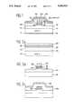
- FIG. 1diagrammatically and in cross-section, a laser structure according to the invention.
- FIG. 2a graph giving the variations of the current density, in amperes/cm 2 , as a function of the voltage in volt applied to heterojunction diodes with or without a supplementary quaternary layer.
- FIGS. 3a to 3cdiagrammatically the different stages in the production of a laser structure according to the invention.
- FIG. 1shows in cross-section, a BRS-type laser structure according to the invention.
- This structurehas a n-type (silicon doped) InP substrate 10 with a doping ion concentration of approximately 5.10 18 ions/cm 3 , an AuTi metal coating 12 on its lower surface 11 and a lower confinement layer of buffer layer 14 on its upper face 13.
- the buffer layer 14is of InP n-doped at a concentration of 5 ⁇ 10 17 to 3 ⁇ 10 18 silicon ions/cm 3 and has a thickness of 0.5 to 2.0 ⁇ m.
- This buffer layer 14supports an active layer 16.
- the layer 16is e.g. of solid, not intentionally doped, quaternary Ga 1-x In x As 1-y P y material with 0 ⁇ x ⁇ 1 and 0 ⁇ y ⁇ 1.
- the residual dopingis of type n with a concentration of approximately 10 16 ions/cm 3 .
- the layer thicknessis approximately 15 nm.
- the composition of the active layer 16can be adjusted as a function of the chosen emission wavelength and in particular so that the laser emits in the range 1.5 or 1.3 ⁇ m.
- Emission at 1.5 ⁇ mcorresponds to x approximately 0.6 and y approximately 0.1 and an emission at 1.3 ⁇ m corresponds to x of approximately 0.75 and y approximately 0.5.
- the active layer 16in the form of a "quantum well" structure constituted by a stack of not intentionally doped (residual n-type) Ga 1-u In u As/Ga 1-x In x As 1-y P y layers, with 0 ⁇ u ⁇ 1 and x and y having the values given above.
- the GaInAs layersconstitute the quantum wells.
- the GaInAsP layersserve as an optical guide and can have a constant or gradual composition.
- the layers used as an optical guidehave a forbidden band width exceeding that of the layers serving as quantum wells.
- These quantum well structuresare also known under the name grating structure.
- the laser structurecan optionally have one or more layers 18 in contact with the active layer made from Ga 1-v In v As 1-w P w with 0 ⁇ v ⁇ 1 and 0 ⁇ w ⁇ 1, which is not intentionally doped (residual n-type) and having a forbidden band width greater than that of the active layer 16, when the latter is of solid GaInAsP, said layers alternating with not intentionally doped InP layers.
- This structureconstitutes a periodic Bragg grating of distributed mirrors.
- a laser equipped with such a Bragg gratingis known as a DFB laser.
- the stack 18has a thickness of approximately 140 nm. It can e.g. consist of a 20 nm thick GaInAsP layer with a v composition in In and w composition in P of respectively 0.75 and 0.5 and two 60 nm thick InP layers.
- This Bragg grating 18optionally supports a layer 20 protecting the active zone and made from p-type InP with a thickness of 0.01 to 0.2 ⁇ m and a doping ion (zinc) concentration of 5.10 17 ions/cm 3 .
- the active layer 16, the Bragg grating layer 18 and the protective layer 20are etched in order to form a ribbon 22 of width 1 between 1 and 3 ⁇ m constituting the active zone of the laser.
- the active ribbon 22is covered by a p-type (zinc doping) InP layer 24 constituting the upper confinement layer.
- the confinement layer 24has on either side of the active zone 22, zones 25 obtained by proton implantation.
- the contact layer 26there is a p + -type Ga 1-f In f As contact layer 26 with 0 ⁇ f ⁇ 1 and a metal coating 28 supported by the contact layer 26.
- the metal coating 28is a TiPt alloy, recharged with gold and having a thickness of 150 nm.
- the contact layere.g. has an indium composition f of 0.53, a thickness of 200 nm and a p-dopant concentration of 5 ⁇ 10 18 to 2 ⁇ 10 19 ions/cm 3 and typically 1 ⁇ 10 19 ions/cm 3 .
- the laser structure shown in FIG. 1differs from those of the prior art by a supplementary quaternary material layer 30 n-doped between 5 ⁇ 10 17 ions/cm 3 and 5 ⁇ 10 18 ions/cm 3 , which is e.g. of Ga 1-z In z As 1-t P t with 0 ⁇ z ⁇ 1 and 0 ⁇ t ⁇ 1 serving as a layer for stopping the diffusion of p-dopant ions (in this case zinc) from the upper confinement layer 24.
- the layer 30protects the active layer 16.
- the layer 30e.g. has the same composition as the active layer 16 (i.e. z and t respectively equal to 0.6 and 0.1 for an emission at 1.5 ⁇ m and z and t respectively 0.75 and 0.5 for an emission at 1.3 ⁇ m) and also forms part of the active zone 22 of the laser. Under these conditions, the layer 30 is also in the form of a ribbon of width 1. Moreover, the thickness of said supplementary layer 30 is less than that of the active layer 16 and is typically 15 nm thick.
- the upper confinement layer 24is p-doped with a doping exceeding 1 ⁇ 10 18 ions/cm 3 and e.g. between 1 ⁇ 10 18 and 1 ⁇ 10 19 ions/cm 3 , said doping typically being 2 ⁇ 10 18 ions/cm 3 .
- the layer 24also has a thickness of 1500 nm.
- An evaluation of the series resistance of the BRS structure according to the inventionleads to a series resistance value below 2 ohms for a device length L, measured in a direction perpendicular to 1 of 250 ⁇ m, i.e. 2 to 5 times less than that of optimized laser structures.
- the Applicanthas carried out various tests and research to verify the essential facts of the invention on the operation of the laser structure, i.e. that of blocking the diffusion of zinc ions by a n-doped Ga 1-z In z As 1-t P t stopping layer, between the Ga 1-x In x As 1-y P y of the active layer and the p-type InP of the upper confinement layer 24.
- acceptorsis accelerated in the presence of holes (p-type material) or decelerated in the presence of electrons (n-type material) a total stoppage of diffusion occurring if the n-dopant concentration exceeds that of the p-acceptors. Moreover, this diffusion is slowed down in GaInAsP materials having a composition varying from InP towards GaInAs.
- the two phenomenaact jointly and it is possible to adjust the thickness of the blocking layer 30 to very small values, e.g. below 20 nm and typically 5 to 15 nm.
- Another important aspect of the inventionrelates to the leakage of current through the parasitic p-n InP junction as a result of the strong p-doping of the layer 24 and the BRS structure.
- the leakage currentis dependent on the direct polarization voltage variation applied to the electrodes for a given current between the active junction and the homojunction.
- a direct voltage increase for a more complex active diodecould eliminate this variation.
- FIG. 2gives the current-voltage characteristics of two heterojunction diodes with and without a supplementary quaternary layer. These diodes have an upper confinement layer p-doped at 2 ⁇ 10 18 ions/cm 3 , a lower, InP confinement layer doped to 1 ⁇ 10 18 ions/cm 3 with a n-dopant and a not intentionally doped, active Ga 1-x In x As 1-y P y layer with x 0.75 and y 0.50.
- the curves a and brespectively give the variations of the current density I, in A/cm 2 , as a function of the voltage V for a diode having a supplementary, quaternary Ga 1-z In z As 1-t P t layer with z 0.75 and t 0.50, which is n + -doped to 1.10 18 ions/cm 3 , between the active layer and the p-doped InP layer and for a diode not having said supplementary layer.
- the laser structure according to the inventionis intended to be produced in two epitaxy stages.
- the process for the production of the laser structure of FIG. 1is shown in FIGS. 3a to 3c.
- depositiontakes place in accordance with the chemical vapor deposition method, using metalorganics (MOVPE) on a n-type InP substrate 10 of a type n, InP buffer layer 14 and a layer 16, which is e.g. of Ga 1-x In x As 1-y P y , which is not intentionally doped and with x and y as given hereinbefore for emitting in the range 1.3 or 1.5 ⁇ m, the Ga 1-z In z As 1-t P t diffusion stopping layer 30 having the same composition of the layer 16, n-doped to 1 ⁇ 10 18 silicon ion/cm 3 , the Bragg grating layer 18 and the p-type, InP protective layer 20.
- MOVPEmetalorganics
- This etchingtakes place in accordance with the preferred crystallographic directions, e.g. in direction ⁇ 110> or ⁇ 110> Chemical etching processes are used and HBr:Br constitutes the etching agent.
- thisis followed by a second MOVPE epitaxy cycle in order to grow the p + -doped, InP layers 24 and the p + -doped, Ga 1-f In f As contact layer 26.
- the upper electrode 28is then produced on the layer 26 using the gold-recharged TiPt metallization deposit.
- the lower TiAu electrode 12is deposited on the face 11 of the InP substrate. This is followed by an ion implantation of protons 25 on either side of the laser ribbon 22, making the p-type, InP layer 24 semi-insulating in the regions 25, in order to electrically insulate the laser ribbon from the remainder of the structure.
- a series resistance of 1.5 ohmwas obtained with this construction having a threshold current of 15 mA and a maximum optical power exceeding 40 mW (max. 90 mW) per face for a device length of 250 ⁇ m.
- the RC product of this constructioni.e. BRS laser with a length of 250 ⁇ m and untreated mirrors
- an equivalent RC diagram of the structurewas deduced.
- the RC value of the structure according to the inventioni.e. 1.5 ohm ⁇ 5 pF
- in low and high frequencyis lower than 8 ps, which corresponds to a passband limit better than 20 GHz.
- the passbands effectively measured on the componentsexceed 16 GHz with a maximum exceeding 18 GHz. They are higher than those of the prior art BRS laser devices.
Landscapes
- Physics & Mathematics (AREA)
- Optics & Photonics (AREA)
- Nanotechnology (AREA)
- Engineering & Computer Science (AREA)
- Chemical & Material Sciences (AREA)
- General Physics & Mathematics (AREA)
- Life Sciences & Earth Sciences (AREA)
- Biophysics (AREA)
- Electromagnetism (AREA)
- Condensed Matter Physics & Semiconductors (AREA)
- Crystallography & Structural Chemistry (AREA)
- Geometry (AREA)
- Semiconductor Lasers (AREA)
Abstract
Description
Claims (8)
Applications Claiming Priority (2)
| Application Number | Priority Date | Filing Date | Title |
|---|---|---|---|
| FR9115000 | 1991-12-04 | ||
| FR9115000AFR2684805B1 (en) | 1991-12-04 | 1991-12-04 | VERY LOW RESISTANCE OPTOELECTRONIC DEVICE. |
Publications (1)
| Publication Number | Publication Date |
|---|---|
| US5306923Atrue US5306923A (en) | 1994-04-26 |
Family
ID=9419648
Family Applications (1)
| Application Number | Title | Priority Date | Filing Date |
|---|---|---|---|
| US07/980,263Expired - LifetimeUS5306923A (en) | 1991-12-04 | 1992-11-23 | Optoelectric device with a very low series resistance |
Country Status (4)
| Country | Link |
|---|---|
| US (1) | US5306923A (en) |
| EP (1) | EP0545808B1 (en) |
| DE (1) | DE69201782T2 (en) |
| FR (1) | FR2684805B1 (en) |
Cited By (33)
| Publication number | Priority date | Publication date | Assignee | Title |
|---|---|---|---|---|
| US20030138016A1 (en)* | 2001-12-07 | 2003-07-24 | The Furukawa Electric Co., Ltd. | Distributed feedback semiconductor laser device |
| US20030209771A1 (en)* | 2000-03-31 | 2003-11-13 | Akulova Yuliya A. | Dopant diffusion blocking for optoelectronic devices using InAlAs or InGaAlAs |
| US20140140653A1 (en)* | 2012-11-16 | 2014-05-22 | Rockwell Collins, Inc. | Transparent waveguide display |
| US10746989B2 (en) | 2015-05-18 | 2020-08-18 | Rockwell Collins, Inc. | Micro collimator system and method for a head up display (HUD) |
| US10795160B1 (en) | 2014-09-25 | 2020-10-06 | Rockwell Collins, Inc. | Systems for and methods of using fold gratings for dual axis expansion |
| US10859768B2 (en) | 2016-03-24 | 2020-12-08 | Digilens Inc. | Method and apparatus for providing a polarization selective holographic waveguide device |
| US10890707B2 (en) | 2016-04-11 | 2021-01-12 | Digilens Inc. | Holographic waveguide apparatus for structured light projection |
| CN112542770A (en)* | 2020-12-04 | 2021-03-23 | 苏州长光华芯光电技术股份有限公司 | Semiconductor device and preparation method thereof |
| US11194098B2 (en) | 2015-02-12 | 2021-12-07 | Digilens Inc. | Waveguide grating device |
| US11194162B2 (en) | 2017-01-05 | 2021-12-07 | Digilens Inc. | Wearable heads up displays |
| US11281013B2 (en) | 2015-10-05 | 2022-03-22 | Digilens Inc. | Apparatus for providing waveguide displays with two-dimensional pupil expansion |
| US11287666B2 (en) | 2011-08-24 | 2022-03-29 | Digilens, Inc. | Wearable data display |
| US11300795B1 (en) | 2009-09-30 | 2022-04-12 | Digilens Inc. | Systems for and methods of using fold gratings coordinated with output couplers for dual axis expansion |
| US11307432B2 (en) | 2014-08-08 | 2022-04-19 | Digilens Inc. | Waveguide laser illuminator incorporating a Despeckler |
| US11366316B2 (en) | 2015-05-18 | 2022-06-21 | Rockwell Collins, Inc. | Head up display (HUD) using a light pipe |
| US11442222B2 (en) | 2019-08-29 | 2022-09-13 | Digilens Inc. | Evacuated gratings and methods of manufacturing |
| US11448937B2 (en) | 2012-11-16 | 2022-09-20 | Digilens Inc. | Transparent waveguide display for tiling a display having plural optical powers using overlapping and offset FOV tiles |
| US11460621B2 (en) | 2012-04-25 | 2022-10-04 | Rockwell Collins, Inc. | Holographic wide angle display |
| US11487131B2 (en) | 2011-04-07 | 2022-11-01 | Digilens Inc. | Laser despeckler based on angular diversity |
| US11513350B2 (en) | 2016-12-02 | 2022-11-29 | Digilens Inc. | Waveguide device with uniform output illumination |
| US11543594B2 (en) | 2019-02-15 | 2023-01-03 | Digilens Inc. | Methods and apparatuses for providing a holographic waveguide display using integrated gratings |
| US11726323B2 (en) | 2014-09-19 | 2023-08-15 | Digilens Inc. | Method and apparatus for generating input images for holographic waveguide displays |
| US11726332B2 (en) | 2009-04-27 | 2023-08-15 | Digilens Inc. | Diffractive projection apparatus |
| US11726329B2 (en) | 2015-01-12 | 2023-08-15 | Digilens Inc. | Environmentally isolated waveguide display |
| US11747568B2 (en) | 2019-06-07 | 2023-09-05 | Digilens Inc. | Waveguides incorporating transmissive and reflective gratings and related methods of manufacturing |
| US12092914B2 (en) | 2018-01-08 | 2024-09-17 | Digilens Inc. | Systems and methods for manufacturing waveguide cells |
| US12140764B2 (en) | 2019-02-15 | 2024-11-12 | Digilens Inc. | Wide angle waveguide display |
| US12158612B2 (en) | 2021-03-05 | 2024-12-03 | Digilens Inc. | Evacuated periodic structures and methods of manufacturing |
| US12210153B2 (en) | 2019-01-14 | 2025-01-28 | Digilens Inc. | Holographic waveguide display with light control layer |
| US12306585B2 (en) | 2018-01-08 | 2025-05-20 | Digilens Inc. | Methods for fabricating optical waveguides |
| US12366823B2 (en) | 2018-01-08 | 2025-07-22 | Digilens Inc. | Systems and methods for high-throughput recording of holographic gratings in waveguide cells |
| US12399326B2 (en) | 2021-01-07 | 2025-08-26 | Digilens Inc. | Grating structures for color waveguides |
| US12397477B2 (en) | 2019-02-05 | 2025-08-26 | Digilens Inc. | Methods for compensating for optical surface nonuniformity |
Citations (10)
| Publication number | Priority date | Publication date | Assignee | Title |
|---|---|---|---|---|
| US4371967A (en)* | 1979-12-19 | 1983-02-01 | Matsushita Electric Industrial Co., Ltd. | Semiconductor laser |
| US4479222A (en)* | 1982-04-27 | 1984-10-23 | The United States Of America As Represented By The Secretary Of The Air Force | Diffusion barrier for long wavelength laser diodes |
| JPS61228684A (en)* | 1985-04-02 | 1986-10-11 | Sumitomo Electric Ind Ltd | semiconductor light emitting device |
| JPS647667A (en)* | 1987-06-30 | 1989-01-11 | Shimadzu Corp | Light-emitting diode of edge emission type |
| EP0380322A2 (en)* | 1989-01-24 | 1990-08-01 | Rohm Co., Ltd. | Semi-conductor lasers |
| JPH04100288A (en)* | 1990-08-20 | 1992-04-02 | Denki Kagaku Kogyo Kk | Semiconductor laser and its manufacture |
| US5177757A (en)* | 1990-06-18 | 1993-01-05 | Mitsubishi Denki Kabushiki Kaisha | Semiconductor laser producing visible light |
| US5189680A (en)* | 1991-04-16 | 1993-02-23 | Mitsubishi Denki Kabushiki Kaisha | Visible light laser diode |
| US5212705A (en)* | 1992-02-18 | 1993-05-18 | Eastman Kodak Company | AlAS Zn-stop diffusion layer in AlGaAs laser diodes |
| US5214663A (en)* | 1991-02-05 | 1993-05-25 | Mitsubishi Denki Kabushiki Kaisha | Semiconductor laser |
- 1991
- 1991-12-04FRFR9115000Apatent/FR2684805B1/ennot_activeExpired - Fee Related
- 1992
- 1992-11-23USUS07/980,263patent/US5306923A/ennot_activeExpired - Lifetime
- 1992-12-01DEDE69201782Tpatent/DE69201782T2/ennot_activeExpired - Fee Related
- 1992-12-01EPEP92403237Apatent/EP0545808B1/ennot_activeExpired - Lifetime
Patent Citations (10)
| Publication number | Priority date | Publication date | Assignee | Title |
|---|---|---|---|---|
| US4371967A (en)* | 1979-12-19 | 1983-02-01 | Matsushita Electric Industrial Co., Ltd. | Semiconductor laser |
| US4479222A (en)* | 1982-04-27 | 1984-10-23 | The United States Of America As Represented By The Secretary Of The Air Force | Diffusion barrier for long wavelength laser diodes |
| JPS61228684A (en)* | 1985-04-02 | 1986-10-11 | Sumitomo Electric Ind Ltd | semiconductor light emitting device |
| JPS647667A (en)* | 1987-06-30 | 1989-01-11 | Shimadzu Corp | Light-emitting diode of edge emission type |
| EP0380322A2 (en)* | 1989-01-24 | 1990-08-01 | Rohm Co., Ltd. | Semi-conductor lasers |
| US5177757A (en)* | 1990-06-18 | 1993-01-05 | Mitsubishi Denki Kabushiki Kaisha | Semiconductor laser producing visible light |
| JPH04100288A (en)* | 1990-08-20 | 1992-04-02 | Denki Kagaku Kogyo Kk | Semiconductor laser and its manufacture |
| US5214663A (en)* | 1991-02-05 | 1993-05-25 | Mitsubishi Denki Kabushiki Kaisha | Semiconductor laser |
| US5189680A (en)* | 1991-04-16 | 1993-02-23 | Mitsubishi Denki Kabushiki Kaisha | Visible light laser diode |
| US5212705A (en)* | 1992-02-18 | 1993-05-18 | Eastman Kodak Company | AlAS Zn-stop diffusion layer in AlGaAs laser diodes |
Non-Patent Citations (4)
| Title |
|---|
| IEEE Journal of Quantum Electronics, vol. 27, No. 6, Jun. 1991 pp. 1794 1797 C. Kazmierski et al.* |
| IEEE Journal of Quantum Electronics, vol. 27, No. 6, Jun. 1991 pp. 1794-1797-C. Kazmierski et al. |
| Japanese Journal of Applied Physics, vol. 25, No. 8, Aug. 1986 pp. 1169 1173 K. Kazmierski et al.* |
| Japanese Journal of Applied Physics, vol. 25, No. 8, Aug. 1986 pp. 1169-1173-K. Kazmierski et al. |
Cited By (54)
| Publication number | Priority date | Publication date | Assignee | Title |
|---|---|---|---|---|
| US20040213313A1 (en)* | 2000-03-31 | 2004-10-28 | Akulova Yuliya A. | Dopant diffusion blocking for optoelectronic devices using InAIAs or InGaAIAs |
| US20030209771A1 (en)* | 2000-03-31 | 2003-11-13 | Akulova Yuliya A. | Dopant diffusion blocking for optoelectronic devices using InAlAs or InGaAlAs |
| US6664605B1 (en)* | 2000-03-31 | 2003-12-16 | Triquint Technology Holding Co. | Dopant diffusion blocking for optoelectronic devices using InAlAs and/or InGaAlAs |
| US20030138016A1 (en)* | 2001-12-07 | 2003-07-24 | The Furukawa Electric Co., Ltd. | Distributed feedback semiconductor laser device |
| US7003013B2 (en)* | 2001-12-07 | 2006-02-21 | The Furukawa Electric Co., Ltd. | Distributed feedback semiconductor laser device |
| US11726332B2 (en) | 2009-04-27 | 2023-08-15 | Digilens Inc. | Diffractive projection apparatus |
| US11300795B1 (en) | 2009-09-30 | 2022-04-12 | Digilens Inc. | Systems for and methods of using fold gratings coordinated with output couplers for dual axis expansion |
| US11487131B2 (en) | 2011-04-07 | 2022-11-01 | Digilens Inc. | Laser despeckler based on angular diversity |
| US12306418B2 (en) | 2011-08-24 | 2025-05-20 | Rockwell Collins, Inc. | Wearable data display |
| US11287666B2 (en) | 2011-08-24 | 2022-03-29 | Digilens, Inc. | Wearable data display |
| US11460621B2 (en) | 2012-04-25 | 2022-10-04 | Rockwell Collins, Inc. | Holographic wide angle display |
| US12276895B2 (en) | 2012-11-16 | 2025-04-15 | Rockwell Collins, Inc. | Transparent waveguide display with passive expander input bragg gratings with different angular diffraction efficiencies |
| US12405507B2 (en) | 2012-11-16 | 2025-09-02 | Digilens Inc. | Transparent waveguide display with grating lamina that both couple and extract modulated light |
| US11320571B2 (en)* | 2012-11-16 | 2022-05-03 | Rockwell Collins, Inc. | Transparent waveguide display providing upper and lower fields of view with uniform light extraction |
| US11815781B2 (en) | 2012-11-16 | 2023-11-14 | Rockwell Collins, Inc. | Transparent waveguide display |
| US11448937B2 (en) | 2012-11-16 | 2022-09-20 | Digilens Inc. | Transparent waveguide display for tiling a display having plural optical powers using overlapping and offset FOV tiles |
| US20140140653A1 (en)* | 2012-11-16 | 2014-05-22 | Rockwell Collins, Inc. | Transparent waveguide display |
| US11307432B2 (en) | 2014-08-08 | 2022-04-19 | Digilens Inc. | Waveguide laser illuminator incorporating a Despeckler |
| US11709373B2 (en) | 2014-08-08 | 2023-07-25 | Digilens Inc. | Waveguide laser illuminator incorporating a despeckler |
| US11726323B2 (en) | 2014-09-19 | 2023-08-15 | Digilens Inc. | Method and apparatus for generating input images for holographic waveguide displays |
| US11579455B2 (en) | 2014-09-25 | 2023-02-14 | Rockwell Collins, Inc. | Systems for and methods of using fold gratings for dual axis expansion using polarized light for wave plates on waveguide faces |
| US10795160B1 (en) | 2014-09-25 | 2020-10-06 | Rockwell Collins, Inc. | Systems for and methods of using fold gratings for dual axis expansion |
| US11726329B2 (en) | 2015-01-12 | 2023-08-15 | Digilens Inc. | Environmentally isolated waveguide display |
| US11194098B2 (en) | 2015-02-12 | 2021-12-07 | Digilens Inc. | Waveguide grating device |
| US11703645B2 (en) | 2015-02-12 | 2023-07-18 | Digilens Inc. | Waveguide grating device |
| US12379547B2 (en) | 2015-02-12 | 2025-08-05 | Digilens Inc. | Waveguide grating device |
| US11366316B2 (en) | 2015-05-18 | 2022-06-21 | Rockwell Collins, Inc. | Head up display (HUD) using a light pipe |
| US10746989B2 (en) | 2015-05-18 | 2020-08-18 | Rockwell Collins, Inc. | Micro collimator system and method for a head up display (HUD) |
| US11754842B2 (en) | 2015-10-05 | 2023-09-12 | Digilens Inc. | Apparatus for providing waveguide displays with two-dimensional pupil expansion |
| US12405471B2 (en) | 2015-10-05 | 2025-09-02 | Digilens Inc. | Apparatus for providing waveguide displays with two-dimensional pupil expansion |
| US11281013B2 (en) | 2015-10-05 | 2022-03-22 | Digilens Inc. | Apparatus for providing waveguide displays with two-dimensional pupil expansion |
| US10859768B2 (en) | 2016-03-24 | 2020-12-08 | Digilens Inc. | Method and apparatus for providing a polarization selective holographic waveguide device |
| US11604314B2 (en) | 2016-03-24 | 2023-03-14 | Digilens Inc. | Method and apparatus for providing a polarization selective holographic waveguide device |
| US10890707B2 (en) | 2016-04-11 | 2021-01-12 | Digilens Inc. | Holographic waveguide apparatus for structured light projection |
| US12298513B2 (en) | 2016-12-02 | 2025-05-13 | Digilens Inc. | Waveguide device with uniform output illumination |
| US11513350B2 (en) | 2016-12-02 | 2022-11-29 | Digilens Inc. | Waveguide device with uniform output illumination |
| US11586046B2 (en) | 2017-01-05 | 2023-02-21 | Digilens Inc. | Wearable heads up displays |
| US11194162B2 (en) | 2017-01-05 | 2021-12-07 | Digilens Inc. | Wearable heads up displays |
| US12248150B2 (en) | 2017-01-05 | 2025-03-11 | Digilens Inc. | Wearable heads up displays |
| US12366823B2 (en) | 2018-01-08 | 2025-07-22 | Digilens Inc. | Systems and methods for high-throughput recording of holographic gratings in waveguide cells |
| US12092914B2 (en) | 2018-01-08 | 2024-09-17 | Digilens Inc. | Systems and methods for manufacturing waveguide cells |
| US12306585B2 (en) | 2018-01-08 | 2025-05-20 | Digilens Inc. | Methods for fabricating optical waveguides |
| US12210153B2 (en) | 2019-01-14 | 2025-01-28 | Digilens Inc. | Holographic waveguide display with light control layer |
| US12397477B2 (en) | 2019-02-05 | 2025-08-26 | Digilens Inc. | Methods for compensating for optical surface nonuniformity |
| US12140764B2 (en) | 2019-02-15 | 2024-11-12 | Digilens Inc. | Wide angle waveguide display |
| US11543594B2 (en) | 2019-02-15 | 2023-01-03 | Digilens Inc. | Methods and apparatuses for providing a holographic waveguide display using integrated gratings |
| US12271035B2 (en) | 2019-06-07 | 2025-04-08 | Digilens Inc. | Waveguides incorporating transmissive and reflective gratings and related methods of manufacturing |
| US11747568B2 (en) | 2019-06-07 | 2023-09-05 | Digilens Inc. | Waveguides incorporating transmissive and reflective gratings and related methods of manufacturing |
| US11592614B2 (en) | 2019-08-29 | 2023-02-28 | Digilens Inc. | Evacuated gratings and methods of manufacturing |
| US11442222B2 (en) | 2019-08-29 | 2022-09-13 | Digilens Inc. | Evacuated gratings and methods of manufacturing |
| US11899238B2 (en) | 2019-08-29 | 2024-02-13 | Digilens Inc. | Evacuated gratings and methods of manufacturing |
| CN112542770A (en)* | 2020-12-04 | 2021-03-23 | 苏州长光华芯光电技术股份有限公司 | Semiconductor device and preparation method thereof |
| US12399326B2 (en) | 2021-01-07 | 2025-08-26 | Digilens Inc. | Grating structures for color waveguides |
| US12158612B2 (en) | 2021-03-05 | 2024-12-03 | Digilens Inc. | Evacuated periodic structures and methods of manufacturing |
Also Published As
| Publication number | Publication date |
|---|---|
| EP0545808B1 (en) | 1995-03-22 |
| FR2684805A1 (en) | 1993-06-11 |
| EP0545808A1 (en) | 1993-06-09 |
| FR2684805B1 (en) | 1998-08-14 |
| DE69201782T2 (en) | 1995-10-05 |
| DE69201782D1 (en) | 1995-04-27 |
Similar Documents
| Publication | Publication Date | Title |
|---|---|---|
| US5306923A (en) | Optoelectric device with a very low series resistance | |
| US6240114B1 (en) | Multi-quantum well lasers with selectively doped barriers | |
| US5381434A (en) | High-temperature, uncooled diode laser | |
| EP1202410A2 (en) | Semiconductor laser device | |
| US6853015B2 (en) | Optical semiconductor device including InGaAlAs doped with Zn | |
| US5107514A (en) | Semiconductor optical element | |
| US8213477B2 (en) | Semiconductor laser and method of manufacturing the same | |
| US5257276A (en) | Strained layer InP/InGaAs quantum well laser | |
| Sakata et al. | All-selective MOVPE-grown 1.3-/spl mu/m strained multi-quantum-well buried-heterostructure laser diodes | |
| US6574258B2 (en) | Semiconductor laser having an active layer provided between two different conduction types of semiconductor layers, and optical modules and communication systems formed therewith | |
| US6560266B2 (en) | Distributed feedback semiconductor laser | |
| JP2677232B2 (en) | Long wavelength semiconductor laser and manufacturing method thereof | |
| Cao et al. | GaInAsP/InP single-quantum-well (SQW) laser with wire-like active region towards quantum wire laser | |
| Sekiguchi et al. | Improvement of current injection uniformity and device resistance in long-wavelength vertical-cavity surface-emitting laser using a tunnel junction | |
| US20080240195A1 (en) | Semiconductor optical device | |
| KR20010020581A (en) | A laser diode of the type having a buried heterostructure | |
| Shimizu et al. | 1.3-/spl mu/m InAsP modulation-doped MQW lasers | |
| US7042921B2 (en) | Complex coupled single mode laser with dual active region | |
| EP0708997B1 (en) | Electrical barrier structure for semiconductor device | |
| Sasaki et al. | Extremely low threshold current operation in 1.5-mu m MQW-DFB laser diodes with semi-insulating InP current blocking region | |
| US5539762A (en) | Article comprising a semiconductor laser with carrier stopper layer | |
| US5170404A (en) | Semiconductor laser device suitable for optical communications systems drive | |
| US20030062517A1 (en) | Semiconductor device with current confinement structure | |
| US4530099A (en) | Planar narrow-stripe laser with improved charge carrier confinement | |
| Jin et al. | Improved performance of 1.3 µm InGaAsP–InP lasers with an AlInAs electron stopper layer |
Legal Events
| Date | Code | Title | Description |
|---|---|---|---|
| AS | Assignment | Owner name:FRANCE TELECOM, FRANCE Free format text:ASSIGNMENT OF ASSIGNORS INTEREST.;ASSIGNORS:KAZMIERSKI, CHRISTOPHE;ROSE, BENOIT;REEL/FRAME:006328/0415 Effective date:19921113 | |
| STCF | Information on status: patent grant | Free format text:PATENTED CASE | |
| FEPP | Fee payment procedure | Free format text:PAYOR NUMBER ASSIGNED (ORIGINAL EVENT CODE: ASPN); ENTITY STATUS OF PATENT OWNER: LARGE ENTITY | |
| FPAY | Fee payment | Year of fee payment:4 | |
| FEPP | Fee payment procedure | Free format text:PAYOR NUMBER ASSIGNED (ORIGINAL EVENT CODE: ASPN); ENTITY STATUS OF PATENT OWNER: LARGE ENTITY | |
| FEPP | Fee payment procedure | Free format text:PAYER NUMBER DE-ASSIGNED (ORIGINAL EVENT CODE: RMPN); ENTITY STATUS OF PATENT OWNER: LARGE ENTITY | |
| FPAY | Fee payment | Year of fee payment:8 | |
| AS | Assignment | Owner name:AVANEX CORPORATION, CALIFORNIA Free format text:ASSIGNMENT OF ASSIGNORS INTEREST;ASSIGNOR:ALCATEL;REEL/FRAME:014083/0431 Effective date:20030731 | |
| AS | Assignment | Owner name:HBK INVESTMENTS L.P., TEXAS Free format text:SECURITY AGREEMENT;ASSIGNOR:AVANEX CORPORATION;REEL/FRAME:016079/0174 Effective date:20050519 | |
| FPAY | Fee payment | Year of fee payment:12 | |
| AS | Assignment | Owner name:AVANEX CORPORATION, CALIFORNIA Free format text:RELEASE BY SECURED PARTY;ASSIGNOR:HBK INVESTMENTS, L.P.;REEL/FRAME:019035/0342 Effective date:20070312 | |
| AS | Assignment | Owner name:WELLS FARGO CAPITAL FINANCE, INC., AS AGENT, CALIF Free format text:PATENT SECURITY AGREEMENT;ASSIGNOR:OCLARO (NORTH AMERICA), INC.;REEL/FRAME:028327/0001 Effective date:20110726 |