US5306659A - Reach-through isolation etching method for silicon-on-insulator devices - Google Patents
Reach-through isolation etching method for silicon-on-insulator devicesDownload PDFInfo
- Publication number
- US5306659A US5306659AUS08/037,855US3785593AUS5306659AUS 5306659 AUS5306659 AUS 5306659AUS 3785593 AUS3785593 AUS 3785593AUS 5306659 AUS5306659 AUS 5306659A
- Authority
- US
- United States
- Prior art keywords
- layer
- trenches
- silicon
- reach
- heavily doped
- Prior art date
- Legal status (The legal status is an assumption and is not a legal conclusion. Google has not performed a legal analysis and makes no representation as to the accuracy of the status listed.)
- Expired - Fee Related
Links
- 238000000034methodMethods0.000titleclaimsabstractdescription12
- 238000005530etchingMethods0.000titleclaimsabstractdescription9
- 238000002955isolationMethods0.000titleabstractdescription7
- 239000012212insulatorSubstances0.000titledescription3
- 229910052710siliconInorganic materials0.000claimsabstractdescription19
- 239000010703siliconSubstances0.000claimsabstractdescription19
- 239000000758substrateSubstances0.000claimsabstractdescription12
- 239000003989dielectric materialSubstances0.000claimsabstractdescription3
- VYPSYNLAJGMNEJ-UHFFFAOYSA-NSilicium dioxideChemical compoundO=[Si]=OVYPSYNLAJGMNEJ-UHFFFAOYSA-N0.000claimsdescription7
- 239000000463materialSubstances0.000claimsdescription4
- 229910021420polycrystalline siliconInorganic materials0.000claimsdescription4
- 229920005591polysiliconPolymers0.000claimsdescription4
- 239000004065semiconductorSubstances0.000claimsdescription3
- 235000012239silicon dioxideNutrition0.000claimsdescription3
- 239000000377silicon dioxideSubstances0.000claimsdescription3
- 239000005388borosilicate glassSubstances0.000claimsdescription2
- 229920000642polymerPolymers0.000claims1
- XUIMIQQOPSSXEZ-UHFFFAOYSA-NSiliconChemical compound[Si]XUIMIQQOPSSXEZ-UHFFFAOYSA-N0.000abstractdescription19
- 238000009792diffusion processMethods0.000abstract2
- 239000011810insulating materialSubstances0.000description2
- 239000004642PolyimideSubstances0.000description1
- 229910007277Si3 N4Inorganic materials0.000description1
- 230000015572biosynthetic processEffects0.000description1
- 230000007717exclusionEffects0.000description1
- 238000003780insertionMethods0.000description1
- 230000037431insertionEffects0.000description1
- 238000004519manufacturing processMethods0.000description1
- 229920001721polyimidePolymers0.000description1
- 229910052814silicon oxideInorganic materials0.000description1
- 230000008646thermal stressEffects0.000description1
Images

Classifications
- H—ELECTRICITY
- H01—ELECTRIC ELEMENTS
- H01L—SEMICONDUCTOR DEVICES NOT COVERED BY CLASS H10
- H01L21/00—Processes or apparatus adapted for the manufacture or treatment of semiconductor or solid state devices or of parts thereof
- H01L21/70—Manufacture or treatment of devices consisting of a plurality of solid state components formed in or on a common substrate or of parts thereof; Manufacture of integrated circuit devices or of parts thereof
- H01L21/71—Manufacture of specific parts of devices defined in group H01L21/70
- H01L21/76—Making of isolation regions between components
- H01L21/762—Dielectric regions, e.g. EPIC dielectric isolation, LOCOS; Trench refilling techniques, SOI technology, use of channel stoppers
- H01L21/7624—Dielectric regions, e.g. EPIC dielectric isolation, LOCOS; Trench refilling techniques, SOI technology, use of channel stoppers using semiconductor on insulator [SOI] technology
- H01L21/76264—SOI together with lateral isolation, e.g. using local oxidation of silicon, or dielectric or polycristalline material refilled trench or air gap isolation regions, e.g. completely isolated semiconductor islands
- H01L21/76286—Lateral isolation by refilling of trenches with polycristalline material
- H—ELECTRICITY
- H01—ELECTRIC ELEMENTS
- H01L—SEMICONDUCTOR DEVICES NOT COVERED BY CLASS H10
- H01L21/00—Processes or apparatus adapted for the manufacture or treatment of semiconductor or solid state devices or of parts thereof
- H01L21/70—Manufacture or treatment of devices consisting of a plurality of solid state components formed in or on a common substrate or of parts thereof; Manufacture of integrated circuit devices or of parts thereof
- H01L21/71—Manufacture of specific parts of devices defined in group H01L21/70
- H01L21/76—Making of isolation regions between components
- H01L21/762—Dielectric regions, e.g. EPIC dielectric isolation, LOCOS; Trench refilling techniques, SOI technology, use of channel stoppers
- H01L21/7624—Dielectric regions, e.g. EPIC dielectric isolation, LOCOS; Trench refilling techniques, SOI technology, use of channel stoppers using semiconductor on insulator [SOI] technology
- H01L21/76264—SOI together with lateral isolation, e.g. using local oxidation of silicon, or dielectric or polycristalline material refilled trench or air gap isolation regions, e.g. completely isolated semiconductor islands
- H01L21/76289—Lateral isolation by air gap
- Y—GENERAL TAGGING OF NEW TECHNOLOGICAL DEVELOPMENTS; GENERAL TAGGING OF CROSS-SECTIONAL TECHNOLOGIES SPANNING OVER SEVERAL SECTIONS OF THE IPC; TECHNICAL SUBJECTS COVERED BY FORMER USPC CROSS-REFERENCE ART COLLECTIONS [XRACs] AND DIGESTS
- Y10—TECHNICAL SUBJECTS COVERED BY FORMER USPC
- Y10S—TECHNICAL SUBJECTS COVERED BY FORMER USPC CROSS-REFERENCE ART COLLECTIONS [XRACs] AND DIGESTS
- Y10S148/00—Metal treatment
- Y10S148/05—Etch and refill
- Y—GENERAL TAGGING OF NEW TECHNOLOGICAL DEVELOPMENTS; GENERAL TAGGING OF CROSS-SECTIONAL TECHNOLOGIES SPANNING OVER SEVERAL SECTIONS OF THE IPC; TECHNICAL SUBJECTS COVERED BY FORMER USPC CROSS-REFERENCE ART COLLECTIONS [XRACs] AND DIGESTS
- Y10—TECHNICAL SUBJECTS COVERED BY FORMER USPC
- Y10S—TECHNICAL SUBJECTS COVERED BY FORMER USPC CROSS-REFERENCE ART COLLECTIONS [XRACs] AND DIGESTS
- Y10S148/00—Metal treatment
- Y10S148/164—Three dimensional processing
Definitions
- the present inventiongenerally relates to silicon-on-insulator semiconductor device structures and methods and, more particularly, to a simplified undercut etching method based on the use of doped reach-through regions to isolate such device structures from each other on the same chip.
- Undercut etching methods to remove selectively a buried doped semiconductive region to form submerged spaces for the insertion of insulating materialare well-known in the silicon-on-insulator (SOI) art.
- SOIsilicon-on-insulator
- the various methodsdiffer in complexity particularly as to how access is gained to each and remove the buried region and as to how the overlying region (to be isolated) is supported during the process of removing the buried region.
- U.S. Pat. No. 4,888,300issued to Gregory N. Burton on Dec. 19, 1989 for Submerged Wall Isolation of Silicon Islands, teaches the use of trenches in an epitaxial layer to provide access to a differently doped buried layer. While supporting the portion of the epitaxial layer adjacent the trench (by an oxide bridge), the underlying region of the buried layer is etched away to form a cavity under the active area. Five etching steps are disclosed to accomplish the accessing, supporting and removal steps for forming the cavity and for completely isolating the silicon islands from the substrate.
- Copending patent application, Ser. No. 07/781,429filed Oct. 23, 1991 in the names of K. D. Beyer et al.
- One object of the present inventionis to eliminate the need to etch a trench, as previously taught to access and to remove a buried region underling each island, in order to isolate each island on the same silicon chip.
- Another object of the present inventionis to eliminate the need to provide an oxide bridge to support each island while a buried region underlying each island is removed.
- a pair of spaced deep trenchesfor defining one dimension of each silicon island to be isolated from a common substrate.
- the trenchesextend from the top surface of a lightly doped silicon layer into the silicon substrate and completely through an intervening heavily doped silicon layer.
- the interior walls of the trenchesare lined with an insulating material such as thermal oxide.
- the third dimension of each islandis established by the thickness of the aforesaid lightly doped silicon layer.
- the heavily doped intervening layer and reach-through diffused areasare removed by a single anisotropic etching step which selectively attacks only the heavily doped regions to the exclusion of the lightly doped and the oxidized regions.
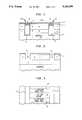
- FIG. 1is a simplified partial cross-sectional view of the partially completed structure of a preferred embodiment showing the lined deep trenches and the layered silicon structure utilized in the present invention
- FIG. 2is a simplified partial cross-sectional view taken along the plane 2--2 of FIG. 1;
- FIG. 3is a plan view of the chip structure of FIGS. 1 and 2;
- FIG. 4is a simplified cross-sectional view corresponding to FIG. 1 but after the central heavily doped region thereof has been removed;
- FIG. 5is a simplified cross-sectional view corresponding to FIG. 2 but after the contiguous heavily doped regions thereof has been removed.
- silicon substrate 1is covered by heavily doped (N + ) epitaxial layer 3 and overlying lightly doped (N - ) epi layer 4.
- the conductivity type of substrate 1is not important in that it is not utilized to form a p-n isolation junction with layer 3.
- Layer 3is replaced by dielectric material, including air, to provide isolation in a manner to be described later.
- a pair of spaced deep trenches 17 and 6define one dimension of a set of isolated silicon islands to be formed in the intervening epi layer 4 separating said trenches. Each trench extends from the top surface 7 of epi layer 4, through epi layer 3 and into substrate 1.
- the interior walls of trenches 17 and 6, as well as the top surface 7 of epi layer 4,are covered by thermal oxide 8.
- a layer 9 of Si 3 N 4covers the top surface portion of oxide 8.
- the trenchespreferably are filled with material 10, 11 such as polysilicon or borosilicate glass and covered with CVD oxide caps 12 and 13.
- a pair of heavily doped (N + ) reach-through regions 14 and 15extend from one trench (17) of FIG. 1 to the next trench (6) of FIG. 1 in a direction perpendicular thereto. Regions 14 and 15 also extend from the top surface 7 of epi layer 4 and into contact with heavily doped (N + ) epi layer 3. Accordingly, reach-through regions 14 and 15 define a second dimension of each isolated silicon island to be formed in the intervening epi layer 4. The third dimension of each island is established by the thickness of layer 4.
- each silicon islandsuch as island 18 of FIG. 3, is attached at opposite ends to the oxidized sidewalls 8 of trenches 17 and 6 and are otherwise surrounded by air dielectric 16 whereby each island is isolated from each other and from substrate 1. Formation of the air dielectric cavity is thus advantageously accomplished using only one selective etching step.
- the space occupied by the air dielectricpreferably is partially filled with a combination of CVD silicon dioxide, polysilicon and/or polymeric material such as a polyimide (not shown), if the described isolation process is done at the end of the hot processing steps for the fabrication of structures within the isolated islands. If the isolated islands are formed prior to such hot processing steps, a sufficiently thick CVD silicon oxide cap is required above the combination-filled regions 16. The presence of the buried air dielectric reduces the amount of any thermal stress that might be encountered.
Landscapes
- Engineering & Computer Science (AREA)
- Physics & Mathematics (AREA)
- Condensed Matter Physics & Semiconductors (AREA)
- General Physics & Mathematics (AREA)
- Manufacturing & Machinery (AREA)
- Computer Hardware Design (AREA)
- Microelectronics & Electronic Packaging (AREA)
- Power Engineering (AREA)
- Element Separation (AREA)
Abstract
Description
The present invention generally relates to silicon-on-insulator semiconductor device structures and methods and, more particularly, to a simplified undercut etching method based on the use of doped reach-through regions to isolate such device structures from each other on the same chip.
Undercut etching methods to remove selectively a buried doped semiconductive region to form submerged spaces for the insertion of insulating material are well-known in the silicon-on-insulator (SOI) art. The various methods differ in complexity particularly as to how access is gained to each and remove the buried region and as to how the overlying region (to be isolated) is supported during the process of removing the buried region.
For example, U.S. Pat. No. 4,888,300, issued to Gregory N. Burton on Dec. 19, 1989 for Submerged Wall Isolation of Silicon Islands, teaches the use of trenches in an epitaxial layer to provide access to a differently doped buried layer. While supporting the portion of the epitaxial layer adjacent the trench (by an oxide bridge), the underlying region of the buried layer is etched away to form a cavity under the active area. Five etching steps are disclosed to accomplish the accessing, supporting and removal steps for forming the cavity and for completely isolating the silicon islands from the substrate. Copending patent application, Ser. No. 07/781,429, filed Oct. 23, 1991 in the names of K. D. Beyer et al. for Buried Air Dielectric Isolation of Silicon Islands and assigned to the present assignee also utilizes trench and oxide bridging steps to provide for the accessing and removal of the buried region material while supporting the active area. Three etching steps are disclosed for forming completely isolated silicon islands.
One object of the present invention is to eliminate the need to etch a trench, as previously taught to access and to remove a buried region underling each island, in order to isolate each island on the same silicon chip.
Another object of the present invention is to eliminate the need to provide an oxide bridge to support each island while a buried region underlying each island is removed.
These and other objects of the invention are achieved by providing a pair of spaced deep trenches for defining one dimension of each silicon island to be isolated from a common substrate. The trenches extend from the top surface of a lightly doped silicon layer into the silicon substrate and completely through an intervening heavily doped silicon layer. The interior walls of the trenches are lined with an insulating material such as thermal oxide. A pair of heavily doped reach-through diffused areas, running fully perpendicularly between the aforesaid trenches and extending from said top surface to said intervening layer, define a second dimension of each silicon island. The third dimension of each island is established by the thickness of the aforesaid lightly doped silicon layer.
The heavily doped intervening layer and reach-through diffused areas are removed by a single anisotropic etching step which selectively attacks only the heavily doped regions to the exclusion of the lightly doped and the oxidized regions.
FIG. 1 is a simplified partial cross-sectional view of the partially completed structure of a preferred embodiment showing the lined deep trenches and the layered silicon structure utilized in the present invention;
FIG. 2 is a simplified partial cross-sectional view taken along theplane 2--2 of FIG. 1;
FIG. 3 is a plan view of the chip structure of FIGS. 1 and 2;
FIG. 4 is a simplified cross-sectional view corresponding to FIG. 1 but after the central heavily doped region thereof has been removed; and
FIG. 5 is a simplified cross-sectional view corresponding to FIG. 2 but after the contiguous heavily doped regions thereof has been removed.
Referring to FIG. 1,silicon substrate 1 is covered by heavily doped (N+)epitaxial layer 3 and overlying lightly doped (N-)epi layer 4. The conductivity type ofsubstrate 1 is not important in that it is not utilized to form a p-n isolation junction withlayer 3.Layer 3 is replaced by dielectric material, including air, to provide isolation in a manner to be described later. A pair of spaceddeep trenches epi layer 4 separating said trenches. Each trench extends from thetop surface 7 ofepi layer 4, throughepi layer 3 and intosubstrate 1. The interior walls oftrenches top surface 7 ofepi layer 4, are covered bythermal oxide 8. Alayer 9 of Si3 N4 covers the top surface portion ofoxide 8. The trenches preferably are filled withmaterial CVD oxide caps
The next feature of the present invention is best shown in the fragmentary cross-sectional view of FIG. 2, taken along theplane 2--2 of FIG. 1 and in the plan view of FIG. 3. A pair of heavily doped (N+) reach-throughregions Regions top surface 7 ofepi layer 4 and into contact with heavily doped (N+)epi layer 3. Accordingly, reach-throughregions epi layer 4. The third dimension of each island is established by the thickness oflayer 4.
The entire structure is subjected to a single selective plasma etch which preferentially attacks and removes the contiguous N+ heavily dopedregions contiguous regions island 18 of FIG. 3, is attached at opposite ends to the oxidizedsidewalls 8 oftrenches substrate 1. Formation of the air dielectric cavity is thus advantageously accomplished using only one selective etching step. The space occupied by the air dielectric preferably is partially filled with a combination of CVD silicon dioxide, polysilicon and/or polymeric material such as a polyimide (not shown), if the described isolation process is done at the end of the hot processing steps for the fabrication of structures within the isolated islands. If the isolated islands are formed prior to such hot processing steps, a sufficiently thick CVD silicon oxide cap is required above the combination-filledregions 16. The presence of the buried air dielectric reduces the amount of any thermal stress that might be encountered.
While the invention has been particularly shown and described with reference to the preferred and alternate embodiments thereof, it will be understood by those skilled in the art that various changes in form and detail may be made therein without departing from the spirit and scope of the invention.
Claims (4)
1. The method of isolating semiconductor islands from a common semiconductor chip comprising the steps of:
providing a first heavily doped epitaxial layer on said substrate;
providing a second lightly doped epitaxial layer on said first layer;
forming a pair of spaced deep trenches extending from the top surface of said second layer, through said first layer and into said substrate;
placing an insulating lining on the interior walls of said trenches;
forming a pair of heavily-doped reach-through regions extending fully between said trenches and from said top surface to said first layer; and
removing said heavily doped layer under said islands and said heavily doped reach-through regions by selective isotropic etching whereby said islands are surrounded by air except where they contact said lined trenches.
2. The method defined in claim 1 and further comprising the step of:
adding dielectric material to said air, said material being selected from the group consisting of silicon dioxide, polysilicon and polymer.
3. The method defined in claim 1 wherein said first and second layers are N+ and N- doped silicon, respectively.
4. The method defined in claim 1 and further comprising the steps of:
filling said deep trenches with one of the group consisting of polysilicon and borosilicate glass; and
capping said one of said group with silicon dioxide.
Priority Applications (4)
| Application Number | Priority Date | Filing Date | Title |
|---|---|---|---|
| US08/037,855US5306659A (en) | 1993-03-29 | 1993-03-29 | Reach-through isolation etching method for silicon-on-insulator devices |
| EP94480017AEP0622843A2 (en) | 1993-03-29 | 1994-02-22 | Reach-through isolation etching method for silicon-on-insulator devices |
| JP6040791AJP2910974B2 (en) | 1993-03-29 | 1994-03-11 | Separation etching method for silicon-on-insulator device |
| US08/231,100US5391911A (en) | 1993-03-29 | 1994-04-22 | Reach-through isolation silicon-on-insulator device |
Applications Claiming Priority (1)
| Application Number | Priority Date | Filing Date | Title |
|---|---|---|---|
| US08/037,855US5306659A (en) | 1993-03-29 | 1993-03-29 | Reach-through isolation etching method for silicon-on-insulator devices |
Related Child Applications (1)
| Application Number | Title | Priority Date | Filing Date |
|---|---|---|---|
| US08/231,100DivisionUS5391911A (en) | 1993-03-29 | 1994-04-22 | Reach-through isolation silicon-on-insulator device |
Publications (1)
| Publication Number | Publication Date |
|---|---|
| US5306659Atrue US5306659A (en) | 1994-04-26 |
Family
ID=21896737
Family Applications (2)
| Application Number | Title | Priority Date | Filing Date |
|---|---|---|---|
| US08/037,855Expired - Fee RelatedUS5306659A (en) | 1993-03-29 | 1993-03-29 | Reach-through isolation etching method for silicon-on-insulator devices |
| US08/231,100Expired - Fee RelatedUS5391911A (en) | 1993-03-29 | 1994-04-22 | Reach-through isolation silicon-on-insulator device |
Family Applications After (1)
| Application Number | Title | Priority Date | Filing Date |
|---|---|---|---|
| US08/231,100Expired - Fee RelatedUS5391911A (en) | 1993-03-29 | 1994-04-22 | Reach-through isolation silicon-on-insulator device |
Country Status (3)
| Country | Link |
|---|---|
| US (2) | US5306659A (en) |
| EP (1) | EP0622843A2 (en) |
| JP (1) | JP2910974B2 (en) |
Cited By (17)
| Publication number | Priority date | Publication date | Assignee | Title |
|---|---|---|---|---|
| US5658164A (en)* | 1995-03-24 | 1997-08-19 | The Whitaker Corporation | Flexible flat electrical cable connector with a conductive shield |
| US5770465A (en)* | 1995-06-23 | 1998-06-23 | Cornell Research Foundation, Inc. | Trench-filling etch-masking microfabrication technique |
| US5950102A (en)* | 1997-02-03 | 1999-09-07 | Industrial Technology Research Institute | Method for fabricating air-insulated multilevel metal interconnections for integrated circuits |
| US6020250A (en)* | 1994-08-11 | 2000-02-01 | International Business Machines Corporation | Stacked devices |
| US6159840A (en)* | 1999-11-12 | 2000-12-12 | United Semiconductor Corp. | Fabrication method for a dual damascene comprising an air-gap |
| US6472257B2 (en)* | 1997-10-23 | 2002-10-29 | Stmicroelectronics S.R.L. | High quality factor, integrated inductor and production method thereof |
| US6518641B2 (en) | 2001-05-18 | 2003-02-11 | International Business Machines Corporation | Deep slit isolation with controlled void |
| US20030098491A1 (en)* | 2001-11-26 | 2003-05-29 | Mitsubishi Denki Kabushiki Kaisha | Semiconductor device with trench isolation and fabrication method thereof |
| KR20040038507A (en)* | 2002-11-01 | 2004-05-08 | 한국전자통신연구원 | Semiconductor device having heat release structure using SOI substrate and method for fabricating the same |
| US20060027889A1 (en)* | 2004-08-05 | 2006-02-09 | International Business Machines Corporation | Isolated fully depleted silicon-on-insulator regions by selective etch |
| US20070222019A1 (en)* | 2004-03-31 | 2007-09-27 | Koninklijke Philips Electronics N.V. | Trench Semiconductor Device and Method of Manufacturing it |
| US20070257312A1 (en)* | 2003-11-27 | 2007-11-08 | Samsung Electronics Co., Ltd. | Semiconductor-on-insulator (soi) substrates and semiconductor devices using void spaces |
| US20090001503A1 (en)* | 2007-06-28 | 2009-01-01 | Samsung Electronics Co., Ltd. | Semiconductor device having floating body element and bulk body element and method of manufacturing the same |
| US20090121312A1 (en)* | 2005-09-01 | 2009-05-14 | Howard Hao Chen | Method and apparatus for making coplanar isolated regions of different semiconductor materials on a substrate |
| US20100117152A1 (en)* | 2007-06-28 | 2010-05-13 | Chang-Woo Oh | Semiconductor devices |
| US8685805B2 (en) | 2004-08-06 | 2014-04-01 | Samsung Electronics Co., Ltd. | Semiconductor devices with connection patterns |
| WO2018057309A1 (en)* | 2016-09-21 | 2018-03-29 | Qualcomm Incorporated | Rf device with reduced substrate coupling |
Families Citing this family (38)
| Publication number | Priority date | Publication date | Assignee | Title |
|---|---|---|---|---|
| JPH07283414A (en)* | 1994-04-05 | 1995-10-27 | Toshiba Corp | MOS semiconductor device |
| US5691230A (en) | 1996-09-04 | 1997-11-25 | Micron Technology, Inc. | Technique for producing small islands of silicon on insulator |
| US5976930A (en) | 1997-04-25 | 1999-11-02 | Micron Technology, Inc. | Method for forming gate segments for an integrated circuit |
| US6004835A (en) | 1997-04-25 | 1999-12-21 | Micron Technology, Inc. | Method of forming integrated circuitry, conductive lines, a conductive grid, a conductive network, an electrical interconnection to anode location and an electrical interconnection with a transistor source/drain region |
| US5892707A (en) | 1997-04-25 | 1999-04-06 | Micron Technology, Inc. | Memory array having a digit line buried in an isolation region and method for forming same |
| US6190960B1 (en) | 1997-04-25 | 2001-02-20 | Micron Technology, Inc. | Method for coupling to semiconductor device in an integrated circuit having edge-defined sub-lithographic conductors |
| US6150687A (en) | 1997-07-08 | 2000-11-21 | Micron Technology, Inc. | Memory cell having a vertical transistor with buried source/drain and dual gates |
| US6072209A (en) | 1997-07-08 | 2000-06-06 | Micro Technology, Inc. | Four F2 folded bit line DRAM cell structure having buried bit and word lines |
| US5936274A (en)* | 1997-07-08 | 1999-08-10 | Micron Technology, Inc. | High density flash memory |
| US6191470B1 (en) | 1997-07-08 | 2001-02-20 | Micron Technology, Inc. | Semiconductor-on-insulator memory cell with buried word and body lines |
| US5909618A (en)* | 1997-07-08 | 1999-06-01 | Micron Technology, Inc. | Method of making memory cell with vertical transistor and buried word and body lines |
| US5973356A (en)* | 1997-07-08 | 1999-10-26 | Micron Technology, Inc. | Ultra high density flash memory |
| US6528837B2 (en) | 1997-10-06 | 2003-03-04 | Micron Technology, Inc. | Circuit and method for an open bit line memory cell with a vertical transistor and trench plate trench capacitor |
| US5907170A (en)* | 1997-10-06 | 1999-05-25 | Micron Technology, Inc. | Circuit and method for an open bit line memory cell with a vertical transistor and trench plate trench capacitor |
| US5914511A (en)* | 1997-10-06 | 1999-06-22 | Micron Technology, Inc. | Circuit and method for a folded bit line memory using trench plate capacitor cells with body bias contacts |
| US6066869A (en)* | 1997-10-06 | 2000-05-23 | Micron Technology, Inc. | Circuit and method for a folded bit line memory cell with vertical transistor and trench capacitor |
| US6025225A (en)* | 1998-01-22 | 2000-02-15 | Micron Technology, Inc. | Circuits with a trench capacitor having micro-roughened semiconductor surfaces and methods for forming the same |
| US6246083B1 (en) | 1998-02-24 | 2001-06-12 | Micron Technology, Inc. | Vertical gain cell and array for a dynamic random access memory |
| US5963469A (en)* | 1998-02-24 | 1999-10-05 | Micron Technology, Inc. | Vertical bipolar read access for low voltage memory cell |
| US6242775B1 (en) | 1998-02-24 | 2001-06-05 | Micron Technology, Inc. | Circuits and methods using vertical complementary transistors |
| US6304483B1 (en) | 1998-02-24 | 2001-10-16 | Micron Technology, Inc. | Circuits and methods for a static random access memory using vertical transistors |
| US6121126A (en)* | 1998-02-25 | 2000-09-19 | Micron Technologies, Inc. | Methods and structures for metal interconnections in integrated circuits |
| US6143655A (en)* | 1998-02-25 | 2000-11-07 | Micron Technology, Inc. | Methods and structures for silver interconnections in integrated circuits |
| US5991225A (en)* | 1998-02-27 | 1999-11-23 | Micron Technology, Inc. | Programmable memory address decode array with vertical transistors |
| US6124729A (en) | 1998-02-27 | 2000-09-26 | Micron Technology, Inc. | Field programmable logic arrays with vertical transistors |
| US6492694B2 (en) | 1998-02-27 | 2002-12-10 | Micron Technology, Inc. | Highly conductive composite polysilicon gate for CMOS integrated circuits |
| US6043527A (en) | 1998-04-14 | 2000-03-28 | Micron Technology, Inc. | Circuits and methods for a memory cell with a trench plate trench capacitor and a vertical bipolar read device |
| US6815303B2 (en)* | 1998-04-29 | 2004-11-09 | Micron Technology, Inc. | Bipolar transistors with low-resistance emitter contacts |
| KR100268878B1 (en)* | 1998-05-08 | 2000-10-16 | 김영환 | Semiconductor device and method for fabricating the same |
| US6093623A (en) | 1998-08-04 | 2000-07-25 | Micron Technology, Inc. | Methods for making silicon-on-insulator structures |
| US6134175A (en) | 1998-08-04 | 2000-10-17 | Micron Technology, Inc. | Memory address decode array with vertical transistors |
| US6208164B1 (en) | 1998-08-04 | 2001-03-27 | Micron Technology, Inc. | Programmable logic array with vertical transistors |
| US6423613B1 (en) | 1998-11-10 | 2002-07-23 | Micron Technology, Inc. | Low temperature silicon wafer bond process with bulk material bond strength |
| US6852167B2 (en) | 2001-03-01 | 2005-02-08 | Micron Technology, Inc. | Methods, systems, and apparatus for uniform chemical-vapor depositions |
| US6568367B2 (en)* | 2001-07-31 | 2003-05-27 | Caterpillar Inc | Engine compression release brake system and method of operation |
| US7160577B2 (en)* | 2002-05-02 | 2007-01-09 | Micron Technology, Inc. | Methods for atomic-layer deposition of aluminum oxides in integrated circuits |
| US7589029B2 (en) | 2002-05-02 | 2009-09-15 | Micron Technology, Inc. | Atomic layer deposition and conversion |
| US7927948B2 (en) | 2005-07-20 | 2011-04-19 | Micron Technology, Inc. | Devices with nanocrystals and methods of formation |
Citations (10)
| Publication number | Priority date | Publication date | Assignee | Title |
|---|---|---|---|---|
| US4418470A (en)* | 1981-10-21 | 1983-12-06 | General Electric Company | Method for fabricating silicon-on-sapphire monolithic microwave integrated circuits |
| US4502913A (en)* | 1982-06-30 | 1985-03-05 | International Business Machines Corporation | Total dielectric isolation for integrated circuits |
| US4619000A (en)* | 1984-09-24 | 1986-10-21 | John Ma | CATV converter having improved tuning circuits |
| US4661832A (en)* | 1982-06-30 | 1987-04-28 | International Business Machines Corporation | Total dielectric isolation for integrated circuits |
| US4810667A (en)* | 1987-04-28 | 1989-03-07 | Texas Instruments Incorporated | Dielectric isolation using isolated silicon by limited anodization of an N+ epitaxially defined sublayer in the presence of a diffusion under film layer |
| US4888300A (en)* | 1985-11-07 | 1989-12-19 | Fairchild Camera And Instrument Corporation | Submerged wall isolation of silicon islands |
| US4925805A (en)* | 1988-04-05 | 1990-05-15 | U.S. Philips Corporation | Method of manufacturing a semiconductor device having an SOI structure using selectable etching |
| US5057450A (en)* | 1991-04-01 | 1991-10-15 | International Business Machines Corporation | Method for fabricating silicon-on-insulator structures |
| US5227658A (en)* | 1991-10-23 | 1993-07-13 | International Business Machines Corporation | Buried air dielectric isolation of silicon islands |
| US5232866A (en)* | 1991-10-23 | 1993-08-03 | International Business Machines Corporation | Isolated films using an air dielectric |
Family Cites Families (2)
| Publication number | Priority date | Publication date | Assignee | Title |
|---|---|---|---|---|
| US4169000A (en)* | 1976-09-02 | 1979-09-25 | International Business Machines Corporation | Method of forming an integrated circuit structure with fully-enclosed air isolation |
| US4104090A (en)* | 1977-02-24 | 1978-08-01 | International Business Machines Corporation | Total dielectric isolation utilizing a combination of reactive ion etching, anodic etching, and thermal oxidation |
- 1993
- 1993-03-29USUS08/037,855patent/US5306659A/ennot_activeExpired - Fee Related
- 1994
- 1994-02-22EPEP94480017Apatent/EP0622843A2/ennot_activeWithdrawn
- 1994-03-11JPJP6040791Apatent/JP2910974B2/ennot_activeExpired - Fee Related
- 1994-04-22USUS08/231,100patent/US5391911A/ennot_activeExpired - Fee Related
Patent Citations (10)
| Publication number | Priority date | Publication date | Assignee | Title |
|---|---|---|---|---|
| US4418470A (en)* | 1981-10-21 | 1983-12-06 | General Electric Company | Method for fabricating silicon-on-sapphire monolithic microwave integrated circuits |
| US4502913A (en)* | 1982-06-30 | 1985-03-05 | International Business Machines Corporation | Total dielectric isolation for integrated circuits |
| US4661832A (en)* | 1982-06-30 | 1987-04-28 | International Business Machines Corporation | Total dielectric isolation for integrated circuits |
| US4619000A (en)* | 1984-09-24 | 1986-10-21 | John Ma | CATV converter having improved tuning circuits |
| US4888300A (en)* | 1985-11-07 | 1989-12-19 | Fairchild Camera And Instrument Corporation | Submerged wall isolation of silicon islands |
| US4810667A (en)* | 1987-04-28 | 1989-03-07 | Texas Instruments Incorporated | Dielectric isolation using isolated silicon by limited anodization of an N+ epitaxially defined sublayer in the presence of a diffusion under film layer |
| US4925805A (en)* | 1988-04-05 | 1990-05-15 | U.S. Philips Corporation | Method of manufacturing a semiconductor device having an SOI structure using selectable etching |
| US5057450A (en)* | 1991-04-01 | 1991-10-15 | International Business Machines Corporation | Method for fabricating silicon-on-insulator structures |
| US5227658A (en)* | 1991-10-23 | 1993-07-13 | International Business Machines Corporation | Buried air dielectric isolation of silicon islands |
| US5232866A (en)* | 1991-10-23 | 1993-08-03 | International Business Machines Corporation | Isolated films using an air dielectric |
Non-Patent Citations (4)
| Title |
|---|
| H. Horie et al., "A New SOI Fabrication Technique for Ultrathin Active Layer of Less the 80nm", 1990 IEEE Symposium on VLSI Technology, pp. 93-94, 1990. |
| H. Horie et al., A New SOI Fabrication Technique for Ultrathin Active Layer of Less the 80nm , 1990 IEEE Symposium on VLSI Technology, pp. 93 94, 1990.* |
| P. E. Cade et al, "Methods of Production Single-Crystal Silicon on Silicon Dioxide", IBM Technical Disclosure Bulletin, vol. 28, No. 5, Oct. 1985, pp. 1855-1856. |
| P. E. Cade et al, Methods of Production Single Crystal Silicon on Silicon Dioxide , IBM Technical Disclosure Bulletin, vol. 28, No. 5, Oct. 1985, pp. 1855 1856.* |
Cited By (23)
| Publication number | Priority date | Publication date | Assignee | Title |
|---|---|---|---|---|
| US6020250A (en)* | 1994-08-11 | 2000-02-01 | International Business Machines Corporation | Stacked devices |
| US5658164A (en)* | 1995-03-24 | 1997-08-19 | The Whitaker Corporation | Flexible flat electrical cable connector with a conductive shield |
| US5770465A (en)* | 1995-06-23 | 1998-06-23 | Cornell Research Foundation, Inc. | Trench-filling etch-masking microfabrication technique |
| US5950102A (en)* | 1997-02-03 | 1999-09-07 | Industrial Technology Research Institute | Method for fabricating air-insulated multilevel metal interconnections for integrated circuits |
| US6472257B2 (en)* | 1997-10-23 | 2002-10-29 | Stmicroelectronics S.R.L. | High quality factor, integrated inductor and production method thereof |
| US6159840A (en)* | 1999-11-12 | 2000-12-12 | United Semiconductor Corp. | Fabrication method for a dual damascene comprising an air-gap |
| US6518641B2 (en) | 2001-05-18 | 2003-02-11 | International Business Machines Corporation | Deep slit isolation with controlled void |
| US20030098491A1 (en)* | 2001-11-26 | 2003-05-29 | Mitsubishi Denki Kabushiki Kaisha | Semiconductor device with trench isolation and fabrication method thereof |
| KR20040038507A (en)* | 2002-11-01 | 2004-05-08 | 한국전자통신연구원 | Semiconductor device having heat release structure using SOI substrate and method for fabricating the same |
| US20100127328A1 (en)* | 2003-11-27 | 2010-05-27 | Samsung Electronics Co., Ltd | Semiconductor-on-insulator (soi) devices using void spaces |
| US20070257312A1 (en)* | 2003-11-27 | 2007-11-08 | Samsung Electronics Co., Ltd. | Semiconductor-on-insulator (soi) substrates and semiconductor devices using void spaces |
| US7394144B2 (en)* | 2004-03-31 | 2008-07-01 | Nxp B.V. | Trench semiconductor device and method of manufacturing it |
| US20070222019A1 (en)* | 2004-03-31 | 2007-09-27 | Koninklijke Philips Electronics N.V. | Trench Semiconductor Device and Method of Manufacturing it |
| US7190007B2 (en) | 2004-08-05 | 2007-03-13 | International Business Machines Corporation | Isolated fully depleted silicon-on-insulator regions by selective etch |
| US20070128776A1 (en)* | 2004-08-05 | 2007-06-07 | International Business Machines Corporation | Isolated fully depleted silicon-on-insulator regions by selective etch |
| US20060027889A1 (en)* | 2004-08-05 | 2006-02-09 | International Business Machines Corporation | Isolated fully depleted silicon-on-insulator regions by selective etch |
| US8685805B2 (en) | 2004-08-06 | 2014-04-01 | Samsung Electronics Co., Ltd. | Semiconductor devices with connection patterns |
| US20090121312A1 (en)* | 2005-09-01 | 2009-05-14 | Howard Hao Chen | Method and apparatus for making coplanar isolated regions of different semiconductor materials on a substrate |
| US7947566B2 (en)* | 2005-09-01 | 2011-05-24 | International Business Machines Corporation | Method and apparatus for making coplanar isolated regions of different semiconductor materials on a substrate |
| US20090001503A1 (en)* | 2007-06-28 | 2009-01-01 | Samsung Electronics Co., Ltd. | Semiconductor device having floating body element and bulk body element and method of manufacturing the same |
| US20100117152A1 (en)* | 2007-06-28 | 2010-05-13 | Chang-Woo Oh | Semiconductor devices |
| US8178924B2 (en) | 2007-06-28 | 2012-05-15 | Samsung Electronic Co., Ltd. | Semiconductor device having floating body element and bulk body element |
| WO2018057309A1 (en)* | 2016-09-21 | 2018-03-29 | Qualcomm Incorporated | Rf device with reduced substrate coupling |
Also Published As
| Publication number | Publication date |
|---|---|
| JPH077075A (en) | 1995-01-10 |
| US5391911A (en) | 1995-02-21 |
| EP0622843A2 (en) | 1994-11-02 |
| JP2910974B2 (en) | 1999-06-23 |
Similar Documents
| Publication | Publication Date | Title |
|---|---|---|
| US5306659A (en) | Reach-through isolation etching method for silicon-on-insulator devices | |
| US5098856A (en) | Air-filled isolation trench with chemically vapor deposited silicon dioxide cap | |
| US5227658A (en) | Buried air dielectric isolation of silicon islands | |
| US6348366B2 (en) | Method of forming conductive lines | |
| US6809368B2 (en) | TTO nitride liner for improved collar protection and TTO reliability | |
| US4785337A (en) | Dynamic ram cell having shared trench storage capacitor with sidewall-defined bridge contacts and gate electrodes | |
| US4888300A (en) | Submerged wall isolation of silicon islands | |
| US4833094A (en) | Method of making a dynamic ram cell having shared trench storage capacitor with sidewall-defined bridge contacts and gate electrodes | |
| US6077740A (en) | Method for forming a semiconductor device contact structure comprising a contour | |
| US5888864A (en) | Manufacturing method of DRAM Cell formed on an insulating layer having a vertical channel | |
| EP0539312A2 (en) | Isolated films using an air dielectric | |
| US6504200B2 (en) | DRAM cell configuration and fabrication method | |
| US4876214A (en) | Method for fabricating an isolation region in a semiconductor substrate | |
| US6399449B1 (en) | Semiconductor circuit using trench isolation and method of fabrication a trench isolator | |
| US5953607A (en) | Buried strap for trench storage capacitors in dram trench cells | |
| KR19980071857A (en) | Bipolar transistor on insulator semiconductor substrate and manufacturing method thereof | |
| US4897702A (en) | Semiconductor memory device and manufacturing method for the same | |
| KR0151040B1 (en) | Device Separation Method of Semiconductor Device | |
| KR940006685B1 (en) | Method of manufacturing semiconductor device having SOI structure | |
| KR0140734B1 (en) | Manufacturing method of semiconductor device | |
| JP2661357B2 (en) | Method for manufacturing semiconductor device | |
| JPH04264765A (en) | Manufacture of semiconductor device | |
| JPH02210848A (en) | Manufacturing method of semiconductor device |
Legal Events
| Date | Code | Title | Description |
|---|---|---|---|
| AS | Assignment | Owner name:INTERNATIONAL BUSINESS MACHINES CORPORATION, NEW Y Free format text:ASSIGNMENT OF ASSIGNORS INTEREST.;ASSIGNORS:BEYER, KLAUS D.;YAPSIR, ANDRIE S.;REEL/FRAME:006503/0266 Effective date:19930324 | |
| FPAY | Fee payment | Year of fee payment:4 | |
| FPAY | Fee payment | Year of fee payment:8 | |
| REMI | Maintenance fee reminder mailed | ||
| LAPS | Lapse for failure to pay maintenance fees | ||
| STCH | Information on status: patent discontinuation | Free format text:PATENT EXPIRED DUE TO NONPAYMENT OF MAINTENANCE FEES UNDER 37 CFR 1.362 | |
| FP | Lapsed due to failure to pay maintenance fee | Effective date:20060426 |