US5302024A - Monolithic microwave power sensor using a heat sensing diode junction - Google Patents
Monolithic microwave power sensor using a heat sensing diode junctionDownload PDFInfo
- Publication number
- US5302024A US5302024AUS08/024,927US2492793AUS5302024AUS 5302024 AUS5302024 AUS 5302024AUS 2492793 AUS2492793 AUS 2492793AUS 5302024 AUS5302024 AUS 5302024A
- Authority
- US
- United States
- Prior art keywords
- substrate
- diode junction
- conversion means
- conductivity
- integrated circuit
- Prior art date
- Legal status (The legal status is an assumption and is not a legal conclusion. Google has not performed a legal analysis and makes no representation as to the accuracy of the status listed.)
- Expired - Lifetime
Links
- 239000000758substrateSubstances0.000claimsabstractdescription40
- 238000006243chemical reactionMethods0.000claimsabstractdescription15
- 229910052751metalInorganic materials0.000claimsdescription17
- 239000002184metalSubstances0.000claimsdescription17
- 230000005540biological transmissionEffects0.000claimsdescription15
- 230000008878couplingEffects0.000claimsdescription3
- 238000010168coupling processMethods0.000claimsdescription3
- 238000005859coupling reactionMethods0.000claimsdescription3
- 238000005468ion implantationMethods0.000claimsdescription3
- 229920002120photoresistant polymerPolymers0.000description12
- 239000004065semiconductorSubstances0.000description6
- JBRZTFJDHDCESZ-UHFFFAOYSA-NAsGaChemical compound[As]#[Ga]JBRZTFJDHDCESZ-UHFFFAOYSA-N0.000description5
- 229910001218Gallium arsenideInorganic materials0.000description5
- 238000010276constructionMethods0.000description5
- PCHJSUWPFVWCPO-UHFFFAOYSA-NgoldChemical compound[Au]PCHJSUWPFVWCPO-UHFFFAOYSA-N0.000description5
- 239000010931goldSubstances0.000description5
- 229910052737goldInorganic materials0.000description5
- 238000000034methodMethods0.000description5
- 230000035945sensitivityEffects0.000description4
- RTAQQCXQSZGOHL-UHFFFAOYSA-NTitaniumChemical compound[Ti]RTAQQCXQSZGOHL-UHFFFAOYSA-N0.000description3
- 238000013461designMethods0.000description3
- 238000005259measurementMethods0.000description3
- 229910052719titaniumInorganic materials0.000description3
- 239000010936titaniumSubstances0.000description3
- PXHVJJICTQNCMI-UHFFFAOYSA-NNickelChemical compound[Ni]PXHVJJICTQNCMI-UHFFFAOYSA-N0.000description2
- 230000008859changeEffects0.000description2
- 230000001419dependent effectEffects0.000description2
- 238000010438heat treatmentMethods0.000description2
- 238000002161passivationMethods0.000description2
- BASFCYQUMIYNBI-UHFFFAOYSA-NplatinumChemical compound[Pt]BASFCYQUMIYNBI-UHFFFAOYSA-N0.000description2
- 230000008569processEffects0.000description2
- 238000012545processingMethods0.000description2
- 239000002904solventSubstances0.000description2
- ZOXJGFHDIHLPTG-UHFFFAOYSA-NBoronChemical compound[B]ZOXJGFHDIHLPTG-UHFFFAOYSA-N0.000description1
- 229910052581Si3N4Inorganic materials0.000description1
- XUIMIQQOPSSXEZ-UHFFFAOYSA-NSiliconChemical group[Si]XUIMIQQOPSSXEZ-UHFFFAOYSA-N0.000description1
- 238000010521absorption reactionMethods0.000description1
- 230000004913activationEffects0.000description1
- 230000015572biosynthetic processEffects0.000description1
- 229910052796boronInorganic materials0.000description1
- 238000004891communicationMethods0.000description1
- 239000013078crystalSubstances0.000description1
- 238000005566electron beam evaporationMethods0.000description1
- 229910052732germaniumInorganic materials0.000description1
- GNPVGFCGXDBREM-UHFFFAOYSA-Ngermanium atomChemical compound[Ge]GNPVGFCGXDBREM-UHFFFAOYSA-N0.000description1
- 238000000227grindingMethods0.000description1
- 238000002955isolationMethods0.000description1
- 239000000463materialSubstances0.000description1
- 238000001465metallisationMethods0.000description1
- 238000012986modificationMethods0.000description1
- 230000004048modificationEffects0.000description1
- 229910052759nickelInorganic materials0.000description1
- 238000001020plasma etchingMethods0.000description1
- 238000007747platingMethods0.000description1
- 229910052697platinumInorganic materials0.000description1
- 230000008439repair processEffects0.000description1
- 238000012827research and developmentMethods0.000description1
- 230000004044responseEffects0.000description1
- HQVNEWCFYHHQES-UHFFFAOYSA-Nsilicon nitrideChemical compoundN12[Si]34N5[Si]62N3[Si]51N64HQVNEWCFYHHQES-UHFFFAOYSA-N0.000description1
- 238000012360testing methodMethods0.000description1
- WFKWXMTUELFFGS-UHFFFAOYSA-NtungstenChemical compound[W]WFKWXMTUELFFGS-UHFFFAOYSA-N0.000description1
- 229910052721tungstenInorganic materials0.000description1
- 239000010937tungstenSubstances0.000description1
Images


Classifications
- G—PHYSICS
- G01—MEASURING; TESTING
- G01R—MEASURING ELECTRIC VARIABLES; MEASURING MAGNETIC VARIABLES
- G01R21/00—Arrangements for measuring electric power or power factor
- G01R21/02—Arrangements for measuring electric power or power factor by thermal methods, e.g. calorimetric
- G01R21/04—Arrangements for measuring electric power or power factor by thermal methods, e.g. calorimetric in circuits having distributed constants
Definitions
- This inventiongenerally relates to microwave power sensors and, in particular, to such sensors which are constructed integrally with a monolithic circuit substrate.
- Various deviceshave been used for sensing microwave power. Such devices typically use one of a variety of sensors for converting microwave energy into heat and measuring the resulting temperature.
- Known devicesinclude Wallaston wires, thermistors and thermocouples mounted in waveguides and coaxial transmission lines.
- the sensing elementis used as a microwave termination requiring that the microwave characteristics of the sensing element be matched to the circuitry or vice versa. For this reason, the sensing elements must be designed to have a low VSWR within the waveguide or coaxial mounting and must also have a temperature dependent electrical characteristic. Because of these requirements, power sensors which are operable over very broad frequency bands have not previously been developed.
- the minimum size of such sensorsis often limited by the need to obtain sufficient temperature sensitivity.
- the various sensorshave a measurable electrical sensitivity to temperature changes.
- Wires and thermistorsvary in conductivity and thermocouples vary in output voltage. If the length of a wire or thermistor is small or the area of dissimilar metal junction of a thermocouple is small, the amount of change in the respective measurable electrical characteristic will also be small. This results in less sensitivity for determining temperature as the size of the sensing element is reduced, and an inherent limitation on the minimum size of such sensors.
- the present inventionto provide a monolithic microwave power sensor operable over wide frequency ranges and having electrically separated microwave and heat sensing components for allowing optimal design and improved temperature sensitivity.
- the deviceprovides a monolithic integrated circuit substrate conversion means formed either on or in the substrate for converting microwave energy into heat, and a thermally sensitive diode junction formed in sufficiently close proximity to the conversion means to be thermally coupled thereto.
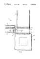
- FIG. 1is an enlarged top plan view of a portion of an integrated circuit including a microwave power sensor constructed in accordance with one embodiment of the present invention
- FIG. 2is a further enlarged top plan view of the portion of FIG. 1 appearing in phantom box 2--2;
- FIG. 3is a sectional view of the components of FIG. 2 taken along view lines 3-3;
- FIG. 4is a schematic of a circuit for producing a signal representing microwave power in response to the sensor of FIGS. 1-3.
- FIG. 1shows a monolithic substrate 10 on which is formed a power sensor 12 constructed in accordance with the present invention.
- a transmission line 14for delivering microwave signals to the device 12, a temperature sensor 16, identical to one included in the device 12, to act as a reference therefor, and a plurality of connector pads 18-21 for making non-microwave electrical connection with the device 12 and temperature sensor 16.
- temperature sensor 16will be discussed with respect to an identical component located within the boundaries of phantom box 2--2.
- the configuration of contacts 18-21is chosen for the present embodiment simply for the convenience of testing purposes. Any variety of circuitry may be used in conformance with known design parameters in adapting the present embodiment for various applications.
- FIG. 2shows details of the power sensing element 12 located at the end of transmission line 14.
- Members of the power sensing element 12generally include a resistor 24, a ground connecting via 26 and a heat sensing diode junction 28.
- Resistor 24is a bulk gallium arsenide construction located at the very end of transmission line 14. It is designed to have the same characteristic impedance and the same width as transmission line 14 for the purposes of acting as a termination thereof and reducing step discontinuities therewith.
- Via 26is constructed at the other end of resistor 24 and passes through the substrate 10 to a ground plane on the other side thereof. This construction provides a well matched termination of transmission line 14 which minimizes the reflection of microwave energy back into the line 14. This insures that substantially all of the microwave energy delivered to transmission line 14 is converted to heat by resistor 24, thus providing greater accuracy to the power measurement.
- Diode junction 28is constructed on and within the substrate 10 in very close proximity to resistor 24 in order to be tightly, thermally coupled thereto.
- Diode junction 28is essentially composed of an ion implanted semiconductor portion 30 formed right in the substrate 10 and a Schottky metal gate structure 32 formed on the surface of substrate 10 and extending over the portion 30.
- FIG. 3shows a sectional view of a portion of the power sensor 12 of FIG. 2 taken along view lines 3--3.
- the substrate 10Generally shown are the substrate 10, a ground plane 34, diode junction 28, and a portion of electrical contact 19.
- the details of FIG. 3are described below in conjunction with the general construction method of the monolithic substrate 10.
- the basic principles of the monolithic construction processare well known as evidenced by the book Monolithic Microwave Integrated Circuits, edited by Robert A. Pucel, 1985, IEEE Press.
- the top surface of the GaAs substrate 10is first polished and cleaned.
- substrate 10is then subjected to ion implantation of silicon atoms to reduce the intrinsic resistivity of the gallium arsenide to a value more suitable for the formation of bulk gallium arsenide resistors and active devices.
- the substrate 10is then thermally annealed to repair crystal lattice damage and to achieve the appropriate activation of the implanted material.
- the heatingis controlled to yield the desired sheet resistance which will provide a (50) ohm resistance from the design specifications of resistor 24. This resistance is also used for active semiconductor device region 30.
- a layer of photoresistis applied to the surface and then patterned and developed to cover the areas which will become resistor 24 and active semiconductor device 30 and to expose the remainder of the surface.
- the exposed areais subjected to ion implantation of boron which raises the resistivity of the exposed substrate back to almost its intrinsic level and thereby isolates resistor 24 and active semiconductor device 30.
- the photoresistis then cleaned off.
- Another layer of photoresistis applied and then patterned and developed to expose the areas which will become ohmic contacts 40,41,42 for resistor 24 and active semiconductor device 30.
- Ohmic contacts 40,41,42are formed on the exposed substrate using gold, germanium and nickel and a suitable metal deposition technique such as electron beam evaporation.
- the photoresistis removed, and the ohmic contacts are suitably sintered to form low resistance electrical connections to the bulk gallium arsenide termination resistor 24 and active semiconductor device 30.
- the substrateis cleaned, and another layer of photoresist is applied and suitably patterned and developed in the shape of the diode junction gate 32.
- the gate patternis then etched to form a slight recess 46 in the surface of substrate 10 and into which recess diode junction gate 32 will be formed.
- Gate 32may then be formed by any suitable process such as inverting the substrate 10 and condensing evaporated titanium, platinum and gold onto the downwardly facing surface.
- Another layer of photoresistis applied to the surface and then patterned and developed to expose the areas which are to become the input transmission line 14, metal bonding pads 18-21, and the topside catch pad 44 for the via 26.
- First metal layers of titanium, tungsten, and goldare deposited on the entire substrate including the photoresist and areas not covered by the photoresist.
- the first metal layersare then removed using a metal liftoff technique in which a solvent is employed to float off the metal on top of the photoresist and leave metal adhered to the substrate forming the basis for transmission line 14, metal bonding pads 18-21, gate connector 39 and the topside catch pad 44.
- the surfaceis cleaned, and a layer of silicon nitride dielectric 48 is applied to serve as a passivation layer for the gate 32.
- a layer of photoresistis applied and patterned and developed to expose areas of the dielectric 48 where no passivation layer is desired. These areas include metal bonding pads 18-21, transmission line 14, and catch pad 44.
- the dielectric layer 48is then removed from undesired areas using reactive ion etching techniques.
- a layer of photoresistis then applied and suitably patterned and developed to expose all areas where thick plated metal is desired, in particular transmission line 14, metal bonding pads 18-21 and catch pad 44.
- a plating interconnect layer of metalis applied and the wafer is electroplated with gold to form thick layers required for transmission line 14, metal bonding pads 18-21 and catch pad 44.
- the substrate 10is next thinned by precision grinding of the backside 50 while the topside of the wafer is protected from damage.
- the backside 50is then patterned and developed to expose an area for via 26, which area is then etched to create a hole 52 extending through to the topside catch pad 44.
- the processing of the waferis completed by applying titanium and gold to form the ground plane layer 34 on the backside of the substrate 10. This layer 34 connects to the topside catch pad 44 to complete the ground connection of via 26.
- microwave signals entering the power sensor 12 through transmission line 14are converted to heat energy which causes the temperature of resistor 24 to rise.
- the tight thermal coupling between diode junction 28 and resistor 24enables the heat from resistor 24 to change the conductivity of diode junction 28.
- FIG. 4shows a circuit 60 for converting the temperature dependent resistance variations of the diode junction 28 into an indication of the amount of microwave energy absorbed by the resistor 24.
- the circuit 60is a bridge network having an operational amplifier 61 to detect the difference between the two branches of the bridge.
- Junction 28is represented as a variable resistance which is matched to the other temperature sensitive diode junction 16.
- Junction 16is constructed on the monolithic substrate 10 to be identical to junction 28. It is constructed during the same processing steps and designed to have the same configuration. Like the junction 28, it is thermally coupled to the substrate 10 in the same manner as junction 28, except for the proximity of resistor 24. Junction 16 is not thermally coupled to resistor 24 but is located in the same general area so that it can act as a reference representing the ambient temperature of substrate 10.
- the bridge circuitalso includes a pair of matched resistors 64,65.
- the difference between the voltages from junctions 28 and 16represent the difference in heating caused by the absorption of microwave energy by resistor 24.
- This voltage differencemay be appropriately scaled in amplifier 61 to provide a measurement of microwave power.
- the present inventionprovides a monolithic microwave power sensor having a very broad frequency range and a very high degree of isolation between microwave and measurement elements.
Landscapes
- Engineering & Computer Science (AREA)
- Power Engineering (AREA)
- Physics & Mathematics (AREA)
- General Physics & Mathematics (AREA)
- Semiconductor Integrated Circuits (AREA)
Abstract
Description
Claims (4)
Priority Applications (1)
| Application Number | Priority Date | Filing Date | Title |
|---|---|---|---|
| US08/024,927US5302024A (en) | 1990-10-09 | 1993-02-26 | Monolithic microwave power sensor using a heat sensing diode junction |
Applications Claiming Priority (3)
| Application Number | Priority Date | Filing Date | Title |
|---|---|---|---|
| US59506690A | 1990-10-09 | 1990-10-09 | |
| US81872392A | 1992-01-06 | 1992-01-06 | |
| US08/024,927US5302024A (en) | 1990-10-09 | 1993-02-26 | Monolithic microwave power sensor using a heat sensing diode junction |
Related Parent Applications (1)
| Application Number | Title | Priority Date | Filing Date |
|---|---|---|---|
| US81872392AContinuation | 1990-10-09 | 1992-01-06 |
Publications (1)
| Publication Number | Publication Date |
|---|---|
| US5302024Atrue US5302024A (en) | 1994-04-12 |
Family
ID=27082144
Family Applications (1)
| Application Number | Title | Priority Date | Filing Date |
|---|---|---|---|
| US08/024,927Expired - LifetimeUS5302024A (en) | 1990-10-09 | 1993-02-26 | Monolithic microwave power sensor using a heat sensing diode junction |
Country Status (1)
| Country | Link |
|---|---|
| US (1) | US5302024A (en) |
Cited By (20)
| Publication number | Priority date | Publication date | Assignee | Title |
|---|---|---|---|---|
| EP0720022A1 (en)* | 1994-12-27 | 1996-07-03 | AT&T Corp. | Thermal detection elements |
| US5713667A (en)* | 1995-06-07 | 1998-02-03 | Advanced Micro Devices, Inc. | Temperature sensing probe for microthermometry |
| WO2001031349A1 (en)* | 1999-10-28 | 2001-05-03 | Centre National De La Recherche Scientifique (Cnrs) | Electromagnetic wave sensor |
| US6361207B1 (en)* | 1999-06-04 | 2002-03-26 | Florida Rf Labs, Inc. | Temperature sensing termination |
| GB2374942A (en)* | 2001-04-26 | 2002-10-30 | Marconi Caswell Ltd | RF sensor using Seebeck effect |
| US20030113644A1 (en)* | 2001-11-02 | 2003-06-19 | Samsung Electronics Co., Ltd. | Electrophotographic organophotoreceptors with novel charge transport compounds |
| US20040057495A1 (en)* | 2002-09-03 | 2004-03-25 | Korea Electonics Technology Institute | Microwave power sensor and method for manufacturing the same |
| US6753807B1 (en)* | 2002-07-30 | 2004-06-22 | The United States Of America As Represented By The Secretary Of Commerce | Combination N-way power divider/combiner and noninvasive reflected power detection |
| US20050116701A1 (en)* | 2002-02-08 | 2005-06-02 | Rohde& Schwarz Gmbh & Co. Kg | Power detector with constant voltage decoupling |
| US6931333B2 (en)* | 2002-05-17 | 2005-08-16 | Bookham Technology Plc | Electrical power sensing |
| US20050279398A1 (en)* | 2004-06-18 | 2005-12-22 | Herrick Katherine J | Microstrip power sensor |
| US20070262359A1 (en)* | 2004-09-02 | 2007-11-15 | International Business Machines Corporation | SELF HEATING MONITOR FOR SiGe AND SOI CMOS DEVICES |
| US20080309488A1 (en)* | 2007-06-15 | 2008-12-18 | Icove David J | Passive microwave fire and intrusion detection system |
| US20100079282A1 (en)* | 2007-06-15 | 2010-04-01 | Icove David J | Passive microwave speed and intrusion detection system |
| CN1885047B (en)* | 2006-06-09 | 2010-04-21 | 东南大学 | Piezoresistive microwave power sensor and microwave power sensing method thereof |
| US20110155397A1 (en)* | 2007-06-15 | 2011-06-30 | Icove And Associates, Llc | Passive microwave system and method for protecting a structure from fire threats |
| CN103149423A (en)* | 2013-03-01 | 2013-06-12 | 东南大学 | Low-temperature double-layer isolating micro-electromechanical system (MEMS) microwave power sensor |
| CN105336757A (en)* | 2015-11-06 | 2016-02-17 | 中国计量学院 | Organic Diode Based Flexible Microwave Energy Converter |
| RU191197U1 (en)* | 2019-05-15 | 2019-07-29 | Федеральное Государственное Унитарное Предприятие "Всероссийский Научно-Исследовательский Институт Физико-Технических И Радиотехнических Измерений" (Фгуп "Вниифтри") | TERMINAL MULTI-PROBE CONVERTER OF TERMINAL TYPE |
| US11422172B2 (en)* | 2018-09-17 | 2022-08-23 | Tegam, Inc. | RF coaxial thermal power sensor |
Citations (13)
| Publication number | Priority date | Publication date | Assignee | Title |
|---|---|---|---|---|
| US3081430A (en)* | 1960-06-06 | 1963-03-12 | Prd Electronics Inc | Microwave power meter of the calorimeter type |
| US3694746A (en)* | 1970-02-09 | 1972-09-26 | Gen Microwave Corp | Thin-film thermoelectric calorimeter for measuring large values of microwave power |
| US3760271A (en)* | 1971-06-07 | 1973-09-18 | Holaday Ind Inc | Microwave survey meter |
| US4044371A (en)* | 1976-09-29 | 1977-08-23 | Honeywell Inc. | Plurality of precise temperature resistors formed in monolithic integrated circuits |
| US4047436A (en)* | 1971-01-28 | 1977-09-13 | Commissariat A L'energie Atomique | Measuring detector and a method of fabrication of said detector |
| SU808950A1 (en)* | 1978-07-07 | 1981-02-28 | Ордена Трудового Красного Знамениинститут Физики Полупроводникован Литовской Ccp | Device for monitoring microwave power |
| SU559130A1 (en)* | 1974-12-02 | 1981-12-23 | Предприятие П/Я Г-4367 | Superhigh frequency power film gauge |
| US4456919A (en)* | 1980-12-30 | 1984-06-26 | Horiba, Ltd. | Thermopile type detector with temperature sensor for cold junction |
| US4733170A (en)* | 1985-05-28 | 1988-03-22 | Marconi Instruments Limited | Microwave power sensors |
| US4789823A (en)* | 1985-11-07 | 1988-12-06 | Rohde & Schwarz Gmbh & Co. Kg | Power sensor for RF power measurements |
| US4854731A (en)* | 1986-08-18 | 1989-08-08 | Siliconix Limited | Temperature sensing apparatus |
| US4968150A (en)* | 1988-03-02 | 1990-11-06 | Asea Brown Boveri Ltd. | Process and arrangement for measuring the energy of a microwave pulse |
| US5100829A (en)* | 1989-08-22 | 1992-03-31 | Motorola, Inc. | Process for forming a semiconductor structure with closely coupled substrate temperature sense element |
- 1993
- 1993-02-26USUS08/024,927patent/US5302024A/ennot_activeExpired - Lifetime
Patent Citations (13)
| Publication number | Priority date | Publication date | Assignee | Title |
|---|---|---|---|---|
| US3081430A (en)* | 1960-06-06 | 1963-03-12 | Prd Electronics Inc | Microwave power meter of the calorimeter type |
| US3694746A (en)* | 1970-02-09 | 1972-09-26 | Gen Microwave Corp | Thin-film thermoelectric calorimeter for measuring large values of microwave power |
| US4047436A (en)* | 1971-01-28 | 1977-09-13 | Commissariat A L'energie Atomique | Measuring detector and a method of fabrication of said detector |
| US3760271A (en)* | 1971-06-07 | 1973-09-18 | Holaday Ind Inc | Microwave survey meter |
| SU559130A1 (en)* | 1974-12-02 | 1981-12-23 | Предприятие П/Я Г-4367 | Superhigh frequency power film gauge |
| US4044371A (en)* | 1976-09-29 | 1977-08-23 | Honeywell Inc. | Plurality of precise temperature resistors formed in monolithic integrated circuits |
| SU808950A1 (en)* | 1978-07-07 | 1981-02-28 | Ордена Трудового Красного Знамениинститут Физики Полупроводникован Литовской Ccp | Device for monitoring microwave power |
| US4456919A (en)* | 1980-12-30 | 1984-06-26 | Horiba, Ltd. | Thermopile type detector with temperature sensor for cold junction |
| US4733170A (en)* | 1985-05-28 | 1988-03-22 | Marconi Instruments Limited | Microwave power sensors |
| US4789823A (en)* | 1985-11-07 | 1988-12-06 | Rohde & Schwarz Gmbh & Co. Kg | Power sensor for RF power measurements |
| US4854731A (en)* | 1986-08-18 | 1989-08-08 | Siliconix Limited | Temperature sensing apparatus |
| US4968150A (en)* | 1988-03-02 | 1990-11-06 | Asea Brown Boveri Ltd. | Process and arrangement for measuring the energy of a microwave pulse |
| US5100829A (en)* | 1989-08-22 | 1992-03-31 | Motorola, Inc. | Process for forming a semiconductor structure with closely coupled substrate temperature sense element |
Non-Patent Citations (1)
| Title |
|---|
| DC to 40 GHz MMIC Power Sensor, Oct. 7, 1990, 1990 IEEE GaAs IC Symposium.* |
Cited By (40)
| Publication number | Priority date | Publication date | Assignee | Title |
|---|---|---|---|---|
| EP0720022A1 (en)* | 1994-12-27 | 1996-07-03 | AT&T Corp. | Thermal detection elements |
| US5713667A (en)* | 1995-06-07 | 1998-02-03 | Advanced Micro Devices, Inc. | Temperature sensing probe for microthermometry |
| US6361207B1 (en)* | 1999-06-04 | 2002-03-26 | Florida Rf Labs, Inc. | Temperature sensing termination |
| US6767128B1 (en) | 1999-10-28 | 2004-07-27 | Centre National De La Recherche Scientifique (Cnrs) | Electromagnetic wave sensor |
| FR2800470A1 (en)* | 1999-10-28 | 2001-05-04 | Centre Nat Rech Scient | ELECTROMAGNETIC WAVE SENSOR. |
| WO2001031349A1 (en)* | 1999-10-28 | 2001-05-03 | Centre National De La Recherche Scientifique (Cnrs) | Electromagnetic wave sensor |
| GB2374942A (en)* | 2001-04-26 | 2002-10-30 | Marconi Caswell Ltd | RF sensor using Seebeck effect |
| GB2374942B (en)* | 2001-04-26 | 2004-07-28 | Marconi Caswell Ltd | Electrical power sensing |
| US20030113644A1 (en)* | 2001-11-02 | 2003-06-19 | Samsung Electronics Co., Ltd. | Electrophotographic organophotoreceptors with novel charge transport compounds |
| US7088089B2 (en)* | 2002-02-08 | 2006-08-08 | Rohde & Schware Gmbh & Co. Kg | Power detector with constant voltage decoupling |
| US20050116701A1 (en)* | 2002-02-08 | 2005-06-02 | Rohde& Schwarz Gmbh & Co. Kg | Power detector with constant voltage decoupling |
| US6931333B2 (en)* | 2002-05-17 | 2005-08-16 | Bookham Technology Plc | Electrical power sensing |
| US6753807B1 (en)* | 2002-07-30 | 2004-06-22 | The United States Of America As Represented By The Secretary Of Commerce | Combination N-way power divider/combiner and noninvasive reflected power detection |
| US6767129B2 (en) | 2002-09-03 | 2004-07-27 | Korea Electronics Technology Institute | Microwave power sensor and method for manufacturing the same |
| US20040057495A1 (en)* | 2002-09-03 | 2004-03-25 | Korea Electonics Technology Institute | Microwave power sensor and method for manufacturing the same |
| US20050279398A1 (en)* | 2004-06-18 | 2005-12-22 | Herrick Katherine J | Microstrip power sensor |
| WO2006007140A1 (en) | 2004-06-18 | 2006-01-19 | Raytheon Company | Microstrip power sensor |
| US7670045B2 (en) | 2004-06-18 | 2010-03-02 | Raytheon Company | Microstrip power sensor |
| US7862233B2 (en)* | 2004-09-02 | 2011-01-04 | International Business Machines Corporation | Self heating monitor for SiGe and SOI CMOS devices |
| US20070262359A1 (en)* | 2004-09-02 | 2007-11-15 | International Business Machines Corporation | SELF HEATING MONITOR FOR SiGe AND SOI CMOS DEVICES |
| US8412487B2 (en) | 2004-09-02 | 2013-04-02 | International Business Machines Corporation | Self heating monitor for SiGe and SOI CMOS devices |
| US20110029274A1 (en)* | 2004-09-02 | 2011-02-03 | International Business Machines Corporation | SELF HEATING MONITOR FOR SiGe AND SOI CMOS DEVICES |
| CN1885047B (en)* | 2006-06-09 | 2010-04-21 | 东南大学 | Piezoresistive microwave power sensor and microwave power sensing method thereof |
| US20100079282A1 (en)* | 2007-06-15 | 2010-04-01 | Icove David J | Passive microwave speed and intrusion detection system |
| US9123220B2 (en) | 2007-06-15 | 2015-09-01 | Icove And Associates, Llc | Passive microwave system and method for protecting a structure from fire threats |
| US7724134B2 (en) | 2007-06-15 | 2010-05-25 | Icove And Associates, Llc | Passive microwave fire and intrusion detection system |
| US7884717B2 (en) | 2007-06-15 | 2011-02-08 | Icove & Associates, Llc | Passive microwave fire and intrusion detection system |
| US20110156721A1 (en)* | 2007-06-15 | 2011-06-30 | Icove And Associates, Llc | Passive microwave fire and intrusion detection system |
| US20110155397A1 (en)* | 2007-06-15 | 2011-06-30 | Icove And Associates, Llc | Passive microwave system and method for protecting a structure from fire threats |
| US8044798B2 (en) | 2007-06-15 | 2011-10-25 | Icove And Associates, Llc | Passive microwave speed and intrusion detection system |
| US8212671B2 (en) | 2007-06-15 | 2012-07-03 | Icove And Associates, Llc | Passive microwave fire and intrusion detection system |
| US20080309488A1 (en)* | 2007-06-15 | 2008-12-18 | Icove David J | Passive microwave fire and intrusion detection system |
| US20100214099A1 (en)* | 2007-06-15 | 2010-08-26 | Icove And Associates, Llc | Passive Microwave Fire and Intrusion Detection System |
| US8493212B2 (en) | 2007-06-15 | 2013-07-23 | Icore and Associates, LLC | Passive microwave system and method for protecting a structure from fire threats |
| CN103149423A (en)* | 2013-03-01 | 2013-06-12 | 东南大学 | Low-temperature double-layer isolating micro-electromechanical system (MEMS) microwave power sensor |
| CN103149423B (en)* | 2013-03-01 | 2015-09-16 | 东南大学 | A kind of low temperature double-layer isolated type MEMS microwave power detector |
| CN105336757A (en)* | 2015-11-06 | 2016-02-17 | 中国计量学院 | Organic Diode Based Flexible Microwave Energy Converter |
| CN105336757B (en)* | 2015-11-06 | 2018-05-15 | 中国计量学院 | Flexible microwave energy converter based on organic diode |
| US11422172B2 (en)* | 2018-09-17 | 2022-08-23 | Tegam, Inc. | RF coaxial thermal power sensor |
| RU191197U1 (en)* | 2019-05-15 | 2019-07-29 | Федеральное Государственное Унитарное Предприятие "Всероссийский Научно-Исследовательский Институт Физико-Технических И Радиотехнических Измерений" (Фгуп "Вниифтри") | TERMINAL MULTI-PROBE CONVERTER OF TERMINAL TYPE |
Similar Documents
| Publication | Publication Date | Title |
|---|---|---|
| US5302024A (en) | Monolithic microwave power sensor using a heat sensing diode junction | |
| US5370458A (en) | Monolithic microwave power sensor | |
| US3758830A (en) | Transducer formed in peripherally supported thin semiconductor web | |
| Klonz et al. | Accurate thin film multijunction thermal converter on a silicon chip (AC-DC standard) | |
| US5450053A (en) | Use of vanadium oxide in microbolometer sensors | |
| US6292140B1 (en) | Antenna for millimeter-wave imaging and bolometer employing the antenna | |
| EP0001707A1 (en) | A thermally isolated monolithic semiconductor die and a process for producing such a die | |
| US6767129B2 (en) | Microwave power sensor and method for manufacturing the same | |
| US4963195A (en) | Electric resistor and a power detector both comprising a thin film conductor | |
| Li et al. | A new RF MEMS power sensor based on double-deck thermocouples with high sensitivity and large dynamic range | |
| US4789823A (en) | Power sensor for RF power measurements | |
| EP0645001B1 (en) | Use of vanadium oxide in microbolometer sensors | |
| US7030453B1 (en) | Bolometric detector with an antenna | |
| US4034313A (en) | Microstrip gunn oscillator with varactor tuning | |
| Deyong et al. | A microstructure semiconductor thermocouple for microwave power sensors | |
| US5148124A (en) | Monolithic microwave integrated circuit noise generator and variable resistance device | |
| US6186661B1 (en) | Schmidt-Boelter gage | |
| Ling et al. | A wide-band monolithic quasi-optical power meter for millimeter-and submillimeter-wave applications | |
| US6767128B1 (en) | Electromagnetic wave sensor | |
| US4272731A (en) | Thin film resistor microwave noise generator | |
| US6259331B1 (en) | YIG oscillator and method of manufacturing the same | |
| US3341785A (en) | Integrated wide-band amplifier system using negative feedback means including a thermally-coupled low-pass thermal filter | |
| US6304229B1 (en) | Electromagnetic wave detecting device incorporating therein a thermocouple | |
| CN1128366C (en) | Microbridge structured thermalcouple type microwave power sensor | |
| Wang et al. | Development research of thermocouple-based microwave power sensors using AC/DC substitution method |
Legal Events
| Date | Code | Title | Description |
|---|---|---|---|
| AS | Assignment | Owner name:LOCKHEED CORPORATION, MARYLAND Free format text:MERGER;ASSIGNOR:SANDERS, LOCKHEED;REEL/FRAME:009463/0029 Effective date:19960125 | |
| FP | Lapsed due to failure to pay maintenance fee | Effective date:19980412 | |
| FEPP | Fee payment procedure | Free format text:PETITION RELATED TO MAINTENANCE FEES FILED (ORIGINAL EVENT CODE: PMFP); ENTITY STATUS OF PATENT OWNER: LARGE ENTITY | |
| FEPP | Fee payment procedure | Free format text:PETITION RELATED TO MAINTENANCE FEES GRANTED (ORIGINAL EVENT CODE: PMFG); ENTITY STATUS OF PATENT OWNER: LARGE ENTITY | |
| FPAY | Fee payment | Year of fee payment:4 | |
| SULP | Surcharge for late payment | ||
| AS | Assignment | Owner name:LOCKHEED MARTIN CORPORATION, MARYLAND Free format text:MERGER;ASSIGNOR:LOCKHEED CORPORATION;REEL/FRAME:010881/0042 Effective date:19960125 | |
| STCF | Information on status: patent grant | Free format text:PATENTED CASE | |
| PRDP | Patent reinstated due to the acceptance of a late maintenance fee | Effective date:20000526 | |
| FEPP | Fee payment procedure | Free format text:PAYOR NUMBER ASSIGNED (ORIGINAL EVENT CODE: ASPN); ENTITY STATUS OF PATENT OWNER: LARGE ENTITY | |
| REMI | Maintenance fee reminder mailed | ||
| FPAY | Fee payment | Year of fee payment:8 | |
| SULP | Surcharge for late payment | Year of fee payment:7 | |
| FPAY | Fee payment | Year of fee payment:12 |