US5301156A - Configurable self-test for embedded RAMs - Google Patents
Configurable self-test for embedded RAMsDownload PDFInfo
- Publication number
- US5301156A US5301156AUS07/732,538US73253891AUS5301156AUS 5301156 AUS5301156 AUS 5301156AUS 73253891 AUS73253891 AUS 73253891AUS 5301156 AUS5301156 AUS 5301156A
- Authority
- US
- United States
- Prior art keywords
- ram
- test
- address
- register
- write
- Prior art date
- Legal status (The legal status is an assumption and is not a legal conclusion. Google has not performed a legal analysis and makes no representation as to the accuracy of the status listed.)
- Expired - Lifetime
Links
- 238000012360testing methodMethods0.000titleclaimsabstractdescription175
- 239000013598vectorSubstances0.000claimsabstractdescription13
- 238000000034methodMethods0.000claimsdescription12
- 238000011990functional testingMethods0.000abstractdescription4
- 238000013459approachMethods0.000description12
- 238000010586diagramMethods0.000description12
- 230000015654memoryEffects0.000description6
- 230000003071parasitic effectEffects0.000description5
- 230000008901benefitEffects0.000description4
- 230000003068static effectEffects0.000description3
- 239000003990capacitorSubstances0.000description2
- 238000004891communicationMethods0.000description2
- 230000008878couplingEffects0.000description2
- 238000010168coupling processMethods0.000description2
- 238000005859coupling reactionMethods0.000description2
- 230000002950deficientEffects0.000description2
- 230000006870functionEffects0.000description2
- 238000004519manufacturing processMethods0.000description2
- 230000007246mechanismEffects0.000description2
- 238000012986modificationMethods0.000description2
- 230000004048modificationEffects0.000description2
- 230000008569processEffects0.000description2
- 238000010998test methodMethods0.000description2
- 101001022148Homo sapiens FurinProteins0.000description1
- 101000701936Homo sapiens Signal peptidase complex subunit 1Proteins0.000description1
- 102100030313Signal peptidase complex subunit 1Human genes0.000description1
- XUIMIQQOPSSXEZ-UHFFFAOYSA-NSiliconChemical compound[Si]XUIMIQQOPSSXEZ-UHFFFAOYSA-N0.000description1
- 239000007795chemical reaction productSubstances0.000description1
- 230000000295complement effectEffects0.000description1
- 230000007812deficiencyEffects0.000description1
- 238000013461designMethods0.000description1
- 238000001514detection methodMethods0.000description1
- 238000011161developmentMethods0.000description1
- 230000000694effectsEffects0.000description1
- 230000005669field effectEffects0.000description1
- 230000010354integrationEffects0.000description1
- 238000001558permutation testMethods0.000description1
- 229910052710siliconInorganic materials0.000description1
- 239000010703siliconSubstances0.000description1
Images


Classifications
- G—PHYSICS
- G01—MEASURING; TESTING
- G01R—MEASURING ELECTRIC VARIABLES; MEASURING MAGNETIC VARIABLES
- G01R31/00—Arrangements for testing electric properties; Arrangements for locating electric faults; Arrangements for electrical testing characterised by what is being tested not provided for elsewhere
- G01R31/28—Testing of electronic circuits, e.g. by signal tracer
- G01R31/317—Testing of digital circuits
- G01R31/3181—Functional testing
- G01R31/3185—Reconfiguring for testing, e.g. LSSD, partitioning
- G01R31/318533—Reconfiguring for testing, e.g. LSSD, partitioning using scanning techniques, e.g. LSSD, Boundary Scan, JTAG
- G01R31/318555—Control logic
- G—PHYSICS
- G11—INFORMATION STORAGE
- G11C—STATIC STORES
- G11C29/00—Checking stores for correct operation ; Subsequent repair; Testing stores during standby or offline operation
- G11C29/04—Detection or location of defective memory elements, e.g. cell constructio details, timing of test signals
- G11C29/08—Functional testing, e.g. testing during refresh, power-on self testing [POST] or distributed testing
- G11C29/12—Built-in arrangements for testing, e.g. built-in self testing [BIST] or interconnection details
- G11C29/18—Address generation devices; Devices for accessing memories, e.g. details of addressing circuits
- G11C29/20—Address generation devices; Devices for accessing memories, e.g. details of addressing circuits using counters or linear-feedback shift registers [LFSR]
- G—PHYSICS
- G11—INFORMATION STORAGE
- G11C—STATIC STORES
- G11C29/00—Checking stores for correct operation ; Subsequent repair; Testing stores during standby or offline operation
- G11C29/04—Detection or location of defective memory elements, e.g. cell constructio details, timing of test signals
- G11C29/08—Functional testing, e.g. testing during refresh, power-on self testing [POST] or distributed testing
- G11C29/48—Arrangements in static stores specially adapted for testing by means external to the store, e.g. using direct memory access [DMA] or using auxiliary access paths
Definitions
- This inventionrelates generally to the art of in-circuit testing of RAMs. More specifically, the invention relates to scanpath testing of RAMs embedded on VLSI chips.
- VLSIdense integration
- Small embedded RAMscan be tested using normal scanpath testing.
- Scanpath testinginvolves interfacing the chip with a RAM tester, and then serially shifting an address, data, and control information into and out of the chip for each RAM address to be tested. Each address requires a shift in, shift out operation.
- This conventional scanpath approachis straightforward and very flexible. Test patterns are easily changed in the tester prior to being shifted into the RAM, and when unexpected failure mechanisms are discovered, the scanpath can be used to access specific RAM addresses such that special tests can be performed to provide detailed diagnostics. Also, a minimal amount of additional chip hardware is required if a scanpath and diagnostic interface port (DIP) are already resident on the chip.
- DIPdiagnostic interface port
- a second test approach for the embedded RAMis to make all RAM signals (i.e., all address lines and data lines) available at the pads of the microchip. This allows the tester to have complete and direct control over the RAM.
- test equipmentmust directly create all test patterns. This requires a special test pattern generator or a tester with a very large amount of vector memory.
- a third test approachis the self-test.
- Conventional (hardware-based) self-testsgenerally use a dedicated controller (i.e., a dedicated state machine such as a programmable logic array) and a data pattern generator which together generate test patterns and then cycle the RAM through a predefined sequence of operations.
- a dedicated controlleri.e., a dedicated state machine such as a programmable logic array
- a data pattern generatorwhich together generate test patterns and then cycle the RAM through a predefined sequence of operations.
- Such a testhas the advantage that it can be run at full speed with a minimum of special hardware or software in the tester.
- the self-testsuffers from the disadvantage that a large amount of on-chip hardware may be required to create the dedicated controller and the data pattern generator. Further, conventional self-tests provide only pass/fail results such that it may not be possible to obtain more detailed diagnostics. In addition, since the test sequence is fixed in hardware, the sequence cannot be modified without modifying the chip. This inflexibility poses a significant problem when unexpected failure mechanisms, which require new tests, are discovered after manufacture of the chip.
- a further shortcoming of self-testis that the dedicated controller normally supplies its control signals to the RAM over a distinct control path such that the regular control path is not tested.
- a configurable self-test circuit and method for testing a RAM embedded in an integrated circuit chipmerges the speed of a conventional self-test with the flexibility of direct scanpath testing to produce a superior RAM test.
- the dedicated state machine of the conventional self-test circuitis replaced with a controller that can be configured through a scanpath.
- the data generator of the self-test circuitis replaced with a scannable write register.
- a signature generatoris used to compile the test results.
- the configurable self-test circuitcomprises an incrementable address register, a configurable control circuit, a write register, a signature generator, and a scanpath.
- the address registerstores the current RAM address to be accessed and is adapted to automatically increment the RAM address by an address increment upon receiving a clock signal.
- the control circuithas a normal operation mode and three test modes wherein all writes, all reads or alternating writes and reads may be performed.
- the write registerstores data patterns which are to be written to the RAM under test.
- the signature generatorreceives data read from the RAM and produces a unique signature. A scanpath through the address register, control circuit, write register, and signature generator allows data to be serially shifted in or out of these devices. A full functional test is performed on the RAM.
- a special testchecks the functioning of the pull-up FETs in each RAM cell. To perform the test, a leak FET is added to each bit and NOT-bit line of the RAM to discharge parasitic capacitances so that false HIGH's can be eliminated.
- FIG. 1is a block diagram of a typical RAM circuit with associated registers.
- FIG. 2is a block diagram of a conventional scannable RAM test circuit.
- FIG. 3is a block diagram of a conventional RAM self-test circuit.
- FIG. 4is a block diagram of the configurable self-test circuit according to the present invention.
- FIG. 5is a state diagram for configurable control circuit 406.
- FIG. 6is a block diagram of incrementable address register 404.
- FIG. 7is a schematic diagram of signature generator 412.
- FIG. 8is a schematic diagram of D flip-flop 702 of signature generator 412 illustrating the scanpath therethrough.
- FIG. 9is a schematic diagram of a static RAM cell configured for the novel pull-up FET test of the present invention.
- a logical HIGHis a TRUE signal and may refer to either a binary "1” or a binary “0” depending on whether the logic used is negative true logic or positive true logic.
- a logical LOWis a FALSE signal and may refer to either a binary "1” or a binary "0” depending on whether the logic used is negative true logic or positive true logic.
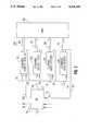
- FIG. 1A block diagram of an embedded RAM (Random Access Memory) circuit 100 is shown in FIG. 1.
- Embedded RAM 100includes RAM 102, an address register 104, a control circuit 106, a write register 108, and a read register 110.
- RAM 102includes read and write latches, and address and control logic, in addition to the RAM memory cells.
- Address register 105is a register somewhere in the data path of the chip which provides address information to RAM 102 via an address bus 105.
- Control circuit 106provides control information to the internal logic of RAM 102 via control bus 107.
- control circuit 106controls address register 104, write register 108, and read register 110.
- Control circuit 106is the controller for the VLSI chip and is normally a programmable logic array (PLA).
- Write register 108provides data which is to be written to RAM 102 via a write bus 109.
- Read register 110accepts data from RAM 102 over a read bus 111.
- Address register 104, write register 108, and read register 110are each connected to a global bus 112.
- RAM 102If a functional test is to be performed on RAM 102, then it must be isolated from its environment, and the test equipment must have access to address bus 105, control bus 107, write bus 109, and read bus 111.
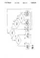
- FIG. 2shows a conventional scannable RAM circuit 200 required to implement normal scanpath testing.
- Scannable RAM circuit 200gains test access to RAM 102 using scannable register cells.
- address register 104is replaced with a scannable address register 204.
- Control circuit 106is replaced with a scannable control circuit 206.
- Write register 108is replaced with a scannable write register 208.
- Read register 110is replaced with a scannable read register 210.
- a "scannable" deviceis a device which can be serially loaded. More specifically, the scannable device is designed with shift registers placed between input/output terminals and the internal logic such that any desired bit pattern can be caused to appear at the normal outputs of the device. When these shift registers are connected together, they form a data register chain known as a scanpath. Scanpaths are well known in the art.
- scannablealso refers to a device which is not inherently scannable, but is connected to a scannable register such that the contents of the scannable register can be dumped into the non-scannable device. This allows any device to be included in a scanpath so long as it is associated with a scannable register.
- Scannable address register 204, scannable control circuit 206, scannable write register 208, and scannable read register 210are connected together to form a scanpath 202.
- a diagnostic interface port (DIP) 214allows communication with scanpath 202.
- DIP 214is also known as a debug port.
- DIP 214is a serial communication port which includes multiplexers and control logic which allow a user to selectively shift data into any one of a plurality of scanpaths.
- the heads 214 and tails 216 of various scanpaths(e.g., scanpath 202) are shown interfacing with DIP 212.
- DIP 212provides a control signal to scannable control circuit 206 over mode line 218.
- the control signalenables alternately selecting either normal operation or test mode for circuit 200.
- Scannable RAM circuit 200operates as follows. RAM test mode is selected via mode line 218. A test vector is then serially shifted in from a tester and into scanpath 202 through DIP 212. Each test vector contains a RAM address (for address register 204) and control information (for control circuit 206). If a write operation is to be performed, then the test vector will also contain a test pattern (for write register 208) which is to be written to the selected RAM address.
- test vectoris shifted into position via scanpath 202, then a clock pulse is supplied to the chip from the tester, and control circuit 206 is cycled. If a read is performed, then the contents of the selected address of RAM 102 will be loaded into read register 210. Similarly, if a write is performed, then the contents of write register 208 will be written to the selected address of RAM 102.
- the contents of the read registermay be shifted out for comparison to an expected value in the tester.
- a next test vectoris then shifted in and the cycle is repeated.
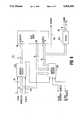
- a conventional RAM self-test circuit 300includes address register 104, control circuit 106, write register 108, and read register 110 as in RAM circuit 100.
- RAM self-test circuit 300includes an address generator 304, a test controller 306, and a data generator 308 which are used to control and sequence RAM 102 through a test.
- Address register 104 and address generator 304are connected to MUX (multiplexer) 305.
- MUX 305is adapted to selectively connect either address register 104 or address generator 304 to RAM 102 via address bus 105.
- Control circuit 106 and test controller 306are connected to MUX (multiplexer) 307.
- MUX 307is adapted to selectively connect either control circuit 106 or test controller 306 to RAM 102 via control bus 107.
- Write register 108 and data generator 308are connected to MUX (multiplexer) 307.
- MUX 309is adapted to selectively connect either write register 108 or data generator 308 to RAM 102 via write bus 109.
- circuit 300Operation of circuit 300 is as follows. MUX's 305, 307, and 309 are controlled by a mode line 302. Mode line 302 is used to select either normal operation of circuit 300 or test mode. During normal operation, address register 104, control circuit 106, and write register 108 are connected to RAM 102, and the VLSI chip operates normally. If test mode is selected, however, MUX 305 will connect address generator 304 to RAM 102, MUX 307 will connect test controller 306 to RAM 102, and MUX 309 will connect data generator 308 to RAM 102.
- Address generator 304, test controller 306, and data generator 308form a dedicated state machine which generates test patterns and cycles RAM 102 through a predefined sequence of read/write operations.
- a data receptor 312is connected to read bus 111. Data receptor 312 accepts the data produced by RAM 102 during read operations and either compares the data to expected results or stores the data for later comparison.
- this self-test approachsuffers from the disadvantage that a large amount of on-chip hardware is required to create dedicated test controller 306 and data generator 308. Further, this test approach will provide only pass/fail results, and the test sequence is fixed in hardware such that it cannot be modified without modifying the chip. Also, note that the normal control path is not tested.
- the present inventionbenefits from the advantages of both scanpath testing and self-test by providing for a configurable self-test.
- the configurable self-testcombines the flexibility of a direct scanpath test with the speed of a conventional self-test by:
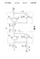
- Configurable self-test circuit 400 of the present inventionis now described with reference to FIG. 4.
- Configurable self-test circuit 400is similar to scannable RAM circuit 200. Note, however, that address register 204 is replaced with an incrementable address register 404.
- Scannable control circuit 206is replaced with a configurable control circuit 406.
- Read register 210is replaced with read register 410.
- a signature generator 412is connected to read bus 111.
- a scanpath 402 through (or allowing access to) incrementable address register 404, configurable control circuit 406, write register 208, and signature generator 412is connected to DIP 212.
- DIP 212further provides a two-bit control signal to configurable control circuit 406 via a mode bus 418.
- the control signalenables selecting either normal operation or one of several test modes for circuit 400.
- configurable control circuit 406is configured via two mode bits (i.e., mode bit [0] and mode bit [1]) from the two control lines of mode bus 418. These two lines allow the tester to select from among four modes of operation: (1) normal operation, (2) test-read on every clock cycle, (3) test-write on every clock cycle, and (4) test-alternating reads and writes.
- configurable control circuit 406is the chip's normal controller.
- the preferred controlleris a PLA.
- the logic for configurable control circuit 406may be any state machine which can do the following for a specified number of cycles:
- a state diagram for control circuit 406is shown in FIG. 5.
- mode bit [0]is checked.
- mode bit [1]is checked. If mode bit [0] is LOW and mode bit [1] is LOW, then control circuit 406 operates normally (i.e., not test mode) at step 508. If mode bit [0] is LOW and mode bit [1] is HIGH, then control circuit 406 outputs write signals at step 510.
- mode bit [0]is HIGH and mode bit [1] is LOW, then control circuit 406 outputs read signals at step 512. If mode bit [0] is HIGH and mode bit [1] is HIGH, then a CYCLE flag is checked at step 514. If the CYCLE flag is LOW, then control circuit 406 outputs write signals at step 516 and sets the CYCLE flag HIGH. If the CYCLE flag is HIGH, then control circuit 406 outputs read signals at step 518 and sets the CYCLE flag LOW.
- Incrementable address register 404is a scannable register.
- register 404is incrementable. That is, register 404 can be automatically incremented by a predetermined amount in either the positive or negative direction. Further, the increment can occur on every clock cycle or every other clock cycle depending on the control pattern loaded into control circuit 406.
- Incrementable address register 404is shown in greater detail in FIG. 6.
- Register 605includes an increment register 602, an adder 604, an address register 606, and a buffer 608.
- Increment register 602is provided to store the address increment.
- Increment register 602has a scanpath input, an address input from global bus 112, and a SETINC (Set Increment) input. A logical HIGH on the SETINC input will cause an address increment on global bus 112 to be loaded into increment register 602. Similarly, increment register 602 may be loaded serially via scanpath 402.
- Increment register 402provides an address increment to a first input of adder 604.
- a second input of adder 604is connected to an output of address register 606.
- Adder 604adds these two addresses to produce an incremented address.
- Address register 606has a scanpath input, an address input from global bus 112, an address input from adder 604, an INCADD (Increment Address) input, and a SETADD (Set Address) input.
- INCADDInc increment Address
- SETADDSet Address
- a logical HIGH on the INCADD inputcauses the incremented address from adder 604 to be loaded as the present address.
- a logical HIGH on the SETADD inputcauses the address from global bus 112 to be loaded into address register 606.
- Address register 606outputs its current address to RAM 102 over address bus 105.
- a buffer 608drives address bus 105.
- incrementable address register 404may be decremented by addition with a two's complement increment such that a dedicated decrement (i.e., count down) feature is not required.
- RAM 102has an 8-bit address word size.
- increment register 602, adder 604, and address register 606are 10-bit devices.
- the 10-bit address word sizeis used to allow configurable self-test circuit 400 to address more than one RAM 102.
- the two most significant bits of the 10-bit address wordmay be used as control bits to select between several RAMs.
- Write register 208is a standard scannable register as is known for scanpath testing.
- read register 410is a simple register located in a data path on the chip. It is not required to be scannable and is not included in scanpath 402. However, it may be scannable and may further be included in scanpath 402 if so desired.
- Signature generator 412is the only piece of hardware which has been added to the integrated circuit which is dedicated entirely to test.
- signature generator 412is a parallel input polynomial signature analyzer which uses a series of linear feedback shift registers to produces a test signature. It should be understood, however, that any device which produces a single number (i.e., a signature) which is statistically related to the correctness of a stream of data may be used for signature generator 412.
- a parity generatoris one such alternate device.
- Polynomial signature analysisis a scheme of logically combining a series of bits in such a manner that statistically there is a very high probability that the logical combination will produce a unique test signature or end product. Since each data term input to the signature generator will effect the unique test signature, comparison with a predetermined, expected signature will indicate whether any data errors have occurred.
- Signature generator 412is a 32-bit shift register which includes thirty-two D flip-flops 702, thirty-two exclusive-OR gates 704, and four inverters 706 connected as shown. Each D flip-flop 702 is a master-slave flip-flop which is scannable. This embodiment of signature generator 412 would be used with a 32-bit word size RAM.
- D flip-flop 702includes a master latch 802, a slave latch 804, and gating transistors 803, 806, 808, and 810.
- Transistor 803is controlled by a CLOCK signal.
- Transistor 806is controlled by a SHIFT signal. The SHIFT signal enables shifting data through signature generator 412 via scanpath 402.
- Transistor 808is controlled by an inverted clock signal, NCLOCK.
- Transistor 810is controlled by an inverted shift signal, NSHIFT. Note that a shift can only occur when CLOCK is LOW and NCLOCK is HIGH.
- signature generator 412may be replaced with other data compilation devices such as an odd/even counter.
- DIP 212No modifications are necessary to DIP 212, as it already contains the hardware necessary to provide control bits and to control the duration (in clock cycles) of a test.
- DIP 212does not have a diagnostic interface port (i.e., DIP 212 is not present)
- four padsmay be added to the chip for the configurable self-test. These include two pads for scanpath 402 and two pads for mode bus 418.
- test modeis selected by the tester via DIP 212 and mode bus 418.
- a test vectoris then serially shifted in from the tester and into scanpath 402 through DIP 212.
- Each test vectorcontains a RAM address (for incrementable address register 404), a control pattern (for configurable control circuit 406), a test pattern (for write register 208), and an initializing signature (i.e., a zero pattern) to be written to polynomial signature generator 412. If desired, each test vector may also include an address increment.
- test vectoris shifted into position via scanpath 402
- a clock signalis supplied to the chip from the tester and configurable control circuit 406 cycles through the entire RAM 102 performing a sequence of reads and writes as specified by the control pattern.
- polynomial signature generator 412monitors and processes the data which is read back from RAM 102. Thereafter, a resulting test signature from signature generator 412 is scanned out via scanpath 402 and compared with an expected signature.
- FIG. 9A schematic diagram of a typical static RAM cell 900 is shown in FIG. 9.
- Cell 900includes FETs 906 and 908, pull-up FETs 902 and 904, and row select FETs 914 and 916.
- Bit line 920is connected to the source side of row select FET 914.
- Nbit (NOT-bit) line 922is connected to the source side of FET 916.
- Row select line 918is connected to the gates of row select FETs 914 and 916.
- Parasitic capacitors 910 and 912are shown (in phantom) connected from the drain side of FETs 914 and 916 respectively.
- a defective or missing pull-up FET (902 or 904)can be difficult to detect. This occurs because parasitic capacitors 910 and 912 may cause the cell to hold a HIGH value from the pre-charge cycle even in the absence of a properly functioning pull-up.
- the present inventionprovides a novel test for the pull-up FETs.
- a leak FET 924is added between bit line 920 and ground.
- a leak FET 926is added between Nbit line 922 and ground.
- a leak FET control line 928is connected to the bases of leak FETs 924 and 926.
- leak FETs 924 and 926are turned ON by either configurable control circuit 406 or DIP 212 via control line 928. Thereby, parasitic capacitances 910 and 912 may be rapidly discharged to avoid a false HIGH condition in the presence of a missing or defective pull-up FET 902 or 904.
- the pull-up FET testmay be performed as follows. A leak FET is connected to each bit line and each NOT-bit line of the RAM. All of the leak FET's are controlled by a single line such that they may be turned ON simultaneously. Prior to the pull-up FET test, all leak FET's are turned ON. A logical HIGH is then written to the RAM address to be tested. The RAM address is then read back, with a HIGH expected. A logical LOW is then written to the RAM cell. Again, the RAM address is read back, with a LOW expected. After the test is completed for all desired addresses, the leak FET's are turned OFF.
- the pull-up FET testis performed along with the other RAM functional tests (e.g., test for shorts, opens, bad prechargers, etc.), and the results may be scanned out (e.g., as a polynomial signature) in the same fashion.
- RAM functional testse.g., test for shorts, opens, bad prechargers, etc.
- test sequenceis now provided to illustrate operation of the invention.
- This test sequencecould be used for a 32-bit word by 512 word RAM which is four words wide (row) and 128 bits high (column).
- This RAMwould have thirty-two bit lines and thirty-two Nbit lines such that sixty-four leak FETs would have to added for the pull-up FET test.
- the RAM addressis stepped by four. This accounts for the fact that the RAM is four words wide and that every fourth address points to an adjacent cell in the next row. Stepping by four allows the tester to test for capacitive coupling, shorts, and other faults which can occur between adjacent memory cells.
- LOADINCREMENTloads an increment value into incrementable address register 404.
- LOADADDRESSloads a starting address into incrementable address register 404.
- LOADWRITELATCHloads a data pattern into write register 208.
- READSIGis the signature which is expected to be shifted out of signature generator 412 at the end of the test.
- WRITEREADis a write to RAM 102 followed by an increment to the address in incrementable address register 404 and a read from RAM 102. The number following the WRITEREAD indicates the number of times the WRITEREAD (i.e., write-increment-read) is to be repeated.
- CLEARSIGclears or resets the signature generator.
- the signature registeris cleared prior to beginning each test. When this is done, the test signature will be a function of the test sequence, and not of any clocking done to load the other registers. As discussed above, this reset may be accomplished through a special function of the signature generator. If the reset is done in this manner, the scan to clear the signature generator may be eliminated.
- test controluses the same output drivers as are used during normal operation, and conventional scanpath testing can be used when required for diagnostics.
- the preferred embodiment described aboveis for application with a single-port RAM.
- the inventionhas equal application to a multi-port RAM, although the exact test will depend on how the ports are used in the chip.
- two signature generatorswould be used.
- the test sequence provided above for the single-port RAMcould be used for the read-write port of the two-port RAM.
- the second signature generatorcould be coupled with the read-only port.
- the read-only portcould then read the same addresses as the read-write port, however, it would be done one half clock cycle behind the read-write port (i.e., the read-only port could be clocked by a clock inverted to the read-write clock).
- the half-cycle delaywould eliminate the potential of receiving an ambiguous read caused by reading during a write.
Landscapes
- Engineering & Computer Science (AREA)
- General Engineering & Computer Science (AREA)
- Physics & Mathematics (AREA)
- General Physics & Mathematics (AREA)
- Techniques For Improving Reliability Of Storages (AREA)
- Tests Of Electronic Circuits (AREA)
- For Increasing The Reliability Of Semiconductor Memories (AREA)
- Static Random-Access Memory (AREA)
Abstract
Description
Claims (12)
Priority Applications (4)
| Application Number | Priority Date | Filing Date | Title |
|---|---|---|---|
| US07/732,538US5301156A (en) | 1991-07-18 | 1991-07-18 | Configurable self-test for embedded RAMs |
| EP92306471AEP0523973B1 (en) | 1991-07-18 | 1992-07-15 | A configurable self-test for embedded RAMs |
| DE69223461TDE69223461T2 (en) | 1991-07-18 | 1992-07-15 | Configurable self-test for integrated RAMs |
| JP19125792AJP3262593B2 (en) | 1991-07-18 | 1992-07-20 | Configurable self-test method and circuit for embedded RAM |
Applications Claiming Priority (1)
| Application Number | Priority Date | Filing Date | Title |
|---|---|---|---|
| US07/732,538US5301156A (en) | 1991-07-18 | 1991-07-18 | Configurable self-test for embedded RAMs |
Publications (1)
| Publication Number | Publication Date |
|---|---|
| US5301156Atrue US5301156A (en) | 1994-04-05 |
Family
ID=24943918
Family Applications (1)
| Application Number | Title | Priority Date | Filing Date |
|---|---|---|---|
| US07/732,538Expired - LifetimeUS5301156A (en) | 1991-07-18 | 1991-07-18 | Configurable self-test for embedded RAMs |
Country Status (4)
| Country | Link |
|---|---|
| US (1) | US5301156A (en) |
| EP (1) | EP0523973B1 (en) |
| JP (1) | JP3262593B2 (en) |
| DE (1) | DE69223461T2 (en) |
Cited By (52)
| Publication number | Priority date | Publication date | Assignee | Title |
|---|---|---|---|---|
| US5428623A (en)* | 1993-07-01 | 1995-06-27 | Tandem Computers Incorporated | Scannable interface to nonscannable microprocessor |
| US5442642A (en)* | 1992-12-11 | 1995-08-15 | Micron Semiconductor, Inc. | Test signal generator on substrate to test |
| US5450455A (en)* | 1993-06-28 | 1995-09-12 | Tandem Computers Incorporated | Method and apparatus for including the states of nonscannable parts in a scan chain |
| US5457781A (en)* | 1993-01-04 | 1995-10-10 | Amdahl Corporation | System having main unit for shutting off clocks to memory upon completion of writing data into memory and information supervising unit to read the data |
| US5515382A (en)* | 1992-07-08 | 1996-05-07 | Sgs-Thomson Microelectronics S.A. | Process for testing the operation of an application specific integrated circuit and application specific integrated circuit relating thereto |
| US5535164A (en)* | 1995-03-03 | 1996-07-09 | International Business Machines Corporation | BIST tester for multiple memories |
| WO1996024135A1 (en)* | 1995-01-30 | 1996-08-08 | Nexcom Technology, Inc. | Memory having adjustable operating characteristics and methods therefor |
| US5617531A (en)* | 1993-11-02 | 1997-04-01 | Motorola, Inc. | Data Processor having a built-in internal self test controller for testing a plurality of memories internal to the data processor |
| US5721863A (en)* | 1996-01-29 | 1998-02-24 | International Business Machines Corporation | Method and structure for accessing semi-associative cache memory using multiple memories to store different components of the address |
| US5768288A (en)* | 1996-03-28 | 1998-06-16 | Cypress Semiconductor Corp. | Method and apparatus for programming a programmable logic device having verify logic for comparing verify data read from a memory location with program data |
| US5771242A (en)* | 1995-06-07 | 1998-06-23 | International Business Machines Corporation | Memory array built-in self-test circuit having a programmable pattern generator for allowing unique read/write operations to adjacent memory cells, and method therefor |
| US5796745A (en)* | 1996-07-19 | 1998-08-18 | International Business Machines Corporation | Memory array built-in self test circuit for testing multi-port memory arrays |
| US5805794A (en)* | 1996-03-28 | 1998-09-08 | Cypress Semiconductor Corp. | CPLD serial programming with extra read register |
| US5815510A (en)* | 1996-03-28 | 1998-09-29 | Cypress Semiconductor Corp. | Serial programming of instruction codes in different numbers of clock cycles |
| US5825785A (en)* | 1996-05-24 | 1998-10-20 | Internaitonal Business Machines Corporation | Serial input shift register built-in self test circuit for embedded circuits |
| US5835503A (en)* | 1996-03-28 | 1998-11-10 | Cypress Semiconductor Corp. | Method and apparatus for serially programming a programmable logic device |
| US5867507A (en)* | 1995-12-12 | 1999-02-02 | International Business Machines Corporation | Testable programmable gate array and associated LSSD/deterministic test methodology |
| US5870410A (en)* | 1996-04-29 | 1999-02-09 | Altera Corporation | Diagnostic interface system for programmable logic system development |
| US5912901A (en)* | 1995-09-18 | 1999-06-15 | International Business Machines Corporation | Method and built-in self-test apparatus for testing an integrated circuit which capture failure information for a selected failure |
| US5918003A (en)* | 1995-06-07 | 1999-06-29 | International Business Machines Corporation | Enhanced built-in self-test circuit and method |
| US5936976A (en)* | 1997-07-25 | 1999-08-10 | Vlsi Technology, Inc. | Selecting a test data input bus to supply test data to logical blocks within an integrated circuit |
| US6001662A (en)* | 1997-12-02 | 1999-12-14 | International Business Machines Corporation | Method and system for providing a reusable configurable self-test controller for manufactured integrated circuits |
| US6061811A (en)* | 1997-10-31 | 2000-05-09 | Texas Instruments Incorporated | Circuits, systems, and methods for external evaluation of microprocessor built-in self-test |
| US6173425B1 (en) | 1998-04-15 | 2001-01-09 | Integrated Device Technology, Inc. | Methods of testing integrated circuits to include data traversal path identification information and related status information in test data streams |
| KR100308621B1 (en)* | 1998-11-19 | 2001-12-17 | 윤종용 | Embedded Programmable Magnetic Test System for Semiconductor Memory Devices |
| US6353903B1 (en) | 1994-10-28 | 2002-03-05 | International Business Machines Corporation | Method and apparatus for testing differential signals |
| US6363501B1 (en)* | 1998-12-10 | 2002-03-26 | Advanced Micro Devices, Inc. | Method and apparatus for saving and loading peripheral device states of a microcontroller via a scan path |
| US6367044B1 (en)* | 1997-11-20 | 2002-04-02 | Mitsubishi Denki Kabushiki Kaisha | Semiconductor integrated circuit device |
| US6459638B1 (en)* | 2001-04-02 | 2002-10-01 | Faraday Technology Corp. | Built-in programmable self-diagnostic circuit for SRAM unit |
| US20030105999A1 (en)* | 2001-12-05 | 2003-06-05 | Koss Louise A. | Apparatus for random access memory array self-test |
| US20030221149A1 (en)* | 2002-05-03 | 2003-11-27 | Jorg Vollrath | Test configuration with automatic test machine and integrated circuit and method for determining the time behavior of an integrated circuit |
| US6670802B2 (en)* | 2000-10-20 | 2003-12-30 | Infineon Technologies Ag | Integrated circuit having a test operating mode and method for testing a multiplicity of such circuits |
| US6678707B1 (en) | 2000-10-30 | 2004-01-13 | Hewlett-Packard Development Company, L.P. | Generation of cryptographically strong random numbers using MISRs |
| DE10232178B3 (en)* | 2002-07-16 | 2004-02-26 | Infineon Technologies Ag | Checking device for address generator for testing device within IC, such as semiconductor memory IC, using storage of values of address signals provided by address generator |
| US6701484B1 (en)* | 2000-08-11 | 2004-03-02 | International Business Machines Corporation | Register file with delayed parity check |
| US6766468B2 (en) | 2001-07-11 | 2004-07-20 | International Business Machines Corporation | Memory BIST and repair |
| US20050024977A1 (en)* | 2000-09-21 | 2005-02-03 | Ong Adrian E. | Multiple power levels for a chip within a multi-chip semiconductor package |
| US20050076279A1 (en)* | 2003-10-07 | 2005-04-07 | International Business Machines Corporation | Method and system for using statistical signatures for testing high-speed circuits |
| US20050162182A1 (en)* | 2002-07-25 | 2005-07-28 | Ong Adrian E. | Internally generating patterns for testing in an integrated circuit device |
| US20050193253A1 (en)* | 2004-02-13 | 2005-09-01 | International Business Machines Corporation | A Command Multiplier for Built-In-Self-Test |
| US20050204223A1 (en)* | 2002-11-27 | 2005-09-15 | Ong Adrian E. | Bonding pads for testing of a semiconductor device |
| US6954879B1 (en) | 1998-12-10 | 2005-10-11 | Advanced Micro Devices, Inc. | Method and apparatus for communicating configuration data for a peripheral device of a microcontroller via a scan path |
| US20050289428A1 (en)* | 2000-09-21 | 2005-12-29 | Sidley Austin Brown & Wood Llp | Architecture and method for testing of an integrated circuit device |
| US20060039211A1 (en)* | 2004-08-20 | 2006-02-23 | Rearick Jeffrey R | Method and apparatus for enabling a user to determine whether a defective location in a memory device has been remapped to a redundant memory portion |
| US20060080584A1 (en)* | 2004-10-07 | 2006-04-13 | Fred Hartnett | Built-in self-test system and method for an integrated circuit |
| US20060107142A1 (en)* | 2004-10-15 | 2006-05-18 | Sony Corporation | Semiconductor integrated circuit |
| US7131043B1 (en)* | 2003-09-25 | 2006-10-31 | Altera Corporation | Automatic testing for programmable networks of control signals |
| US20070067687A1 (en)* | 2001-09-28 | 2007-03-22 | Ong Adrian E | Integrated Circuit Testing Module Configured for Set-up and Hold Time Testing |
| US20070079204A1 (en)* | 2001-09-28 | 2007-04-05 | Ong Adrian E | Integrated Circuit Testing Module Including Signal Shaping Interface |
| US20080148007A1 (en)* | 2006-12-15 | 2008-06-19 | Joo-Sang Lee | Method and apparatus for selectively utilizing information within a semiconductor device |
| US8063650B2 (en) | 2002-11-27 | 2011-11-22 | Rambus Inc. | Testing fuse configurations in semiconductor devices |
| US8286046B2 (en) | 2001-09-28 | 2012-10-09 | Rambus Inc. | Integrated circuit testing module including signal shaping interface |
Families Citing this family (5)
| Publication number | Priority date | Publication date | Assignee | Title |
|---|---|---|---|---|
| US5668815A (en)* | 1996-08-14 | 1997-09-16 | Advanced Micro Devices, Inc. | Method for testing integrated memory using an integrated DMA controller |
| US7073100B2 (en) | 2002-11-11 | 2006-07-04 | International Business Machines Corporation | Method for testing embedded DRAM arrays |
| US6959256B2 (en)* | 2003-05-16 | 2005-10-25 | Analog Devices, Inc. | Universally accessible fully programmable memory built-in self-test (MBIST) system and method |
| CN103680639B (en)* | 2013-11-29 | 2016-08-24 | 西安空间无线电技术研究所 | The periodicity of a kind of random access memory is from error detection restoration methods |
| CN104932954B (en)* | 2015-07-01 | 2017-10-24 | 西北工业大学 | Microsatellite FPGA critical data guard methods |
Citations (4)
| Publication number | Priority date | Publication date | Assignee | Title |
|---|---|---|---|---|
| US4601034A (en)* | 1984-03-30 | 1986-07-15 | Texas Instruments Incorporated | Method and apparatus for testing very large scale integrated memory circuits |
| US4827476A (en)* | 1987-04-16 | 1989-05-02 | Tandem Computers Incorporated | Scan test apparatus for digital systems having dynamic random access memory |
| US4918378A (en)* | 1989-06-12 | 1990-04-17 | Unisys Corporation | Method and circuitry for enabling internal test operations in a VLSI chip |
| US5006787A (en)* | 1989-06-12 | 1991-04-09 | Unisys Corporation | Self-testing circuitry for VLSI units |
Family Cites Families (3)
| Publication number | Priority date | Publication date | Assignee | Title |
|---|---|---|---|---|
| JPS62140299A (en)* | 1985-12-13 | 1987-06-23 | Advantest Corp | Pattern generating device |
| US4879690A (en)* | 1987-09-07 | 1989-11-07 | Mitsubishi Denki Kabushiki Kaisha | Static random access memory with reduced soft error rate |
| JPH0820967B2 (en)* | 1987-09-25 | 1996-03-04 | 三菱電機株式会社 | Integrated circuit |
- 1991
- 1991-07-18USUS07/732,538patent/US5301156A/ennot_activeExpired - Lifetime
- 1992
- 1992-07-15DEDE69223461Tpatent/DE69223461T2/ennot_activeExpired - Fee Related
- 1992-07-15EPEP92306471Apatent/EP0523973B1/ennot_activeExpired - Lifetime
- 1992-07-20JPJP19125792Apatent/JP3262593B2/ennot_activeExpired - Fee Related
Patent Citations (4)
| Publication number | Priority date | Publication date | Assignee | Title |
|---|---|---|---|---|
| US4601034A (en)* | 1984-03-30 | 1986-07-15 | Texas Instruments Incorporated | Method and apparatus for testing very large scale integrated memory circuits |
| US4827476A (en)* | 1987-04-16 | 1989-05-02 | Tandem Computers Incorporated | Scan test apparatus for digital systems having dynamic random access memory |
| US4918378A (en)* | 1989-06-12 | 1990-04-17 | Unisys Corporation | Method and circuitry for enabling internal test operations in a VLSI chip |
| US5006787A (en)* | 1989-06-12 | 1991-04-09 | Unisys Corporation | Self-testing circuitry for VLSI units |
Non-Patent Citations (8)
| Title |
|---|
| Dekker, R., et al. "Fault Modeling and Test Algorighm Development for Static Random Access Memories," Proc. IEEE Int'l Test Conf., Sep. 1988, pp. 343-352 (IEEE Order No. CH2610-45/88/0000/0343$01.00). |
| Dekker, R., et al. "Realistic Built-in Self-test for Static RAMs," IEEE Design & Test of Computers, Feb. 1989, pp. 26-354, (IEEE Order No. 0740-7475/89/002-26$1.00). |
| Dekker, R., et al. Fault Modeling and Test Algorighm Development for Static Random Access Memories, Proc. IEEE Int l Test Conf., Sep. 1988, pp. 343 352 (IEEE Order No. CH2610 45/88/0000/0343$01.00).* |
| Dekker, R., et al. Realistic Built in Self test for Static RAMs, IEEE Design & Test of Computers, Feb. 1989, pp. 26 354, (IEEE Order No. 0740 7475/89/002 26$1.00).* |
| Frowerk, R., "Signature Analysis: A New Digital Field Service Method," Hewlett Packard Journal, 1977. |
| Frowerk, R., Signature Analysis: A New Digital Field Service Method, Hewlett Packard Journal, 1977.* |
| Hassan, S., et al., "Parallel Signature Analyzers-Detection Capability and Extensions," Apr. 1983, (IEEE order number 4/83/0000-0440$1.00). |
| Hassan, S., et al., Parallel Signature Analyzers Detection Capability and Extensions, Apr. 1983, (IEEE order number 4/83/0000 0440$1.00).* |
Cited By (85)
| Publication number | Priority date | Publication date | Assignee | Title |
|---|---|---|---|---|
| US5515382A (en)* | 1992-07-08 | 1996-05-07 | Sgs-Thomson Microelectronics S.A. | Process for testing the operation of an application specific integrated circuit and application specific integrated circuit relating thereto |
| US5499250A (en)* | 1992-12-11 | 1996-03-12 | Micron Technology Inc. | System having multiple subsystems and test signal source resident upon common substrate |
| US5442642A (en)* | 1992-12-11 | 1995-08-15 | Micron Semiconductor, Inc. | Test signal generator on substrate to test |
| US5648974A (en)* | 1992-12-11 | 1997-07-15 | Micron Technology, Inc. | System having multiple subsystems and test signal source resident upon common substrate |
| US5457781A (en)* | 1993-01-04 | 1995-10-10 | Amdahl Corporation | System having main unit for shutting off clocks to memory upon completion of writing data into memory and information supervising unit to read the data |
| US5450455A (en)* | 1993-06-28 | 1995-09-12 | Tandem Computers Incorporated | Method and apparatus for including the states of nonscannable parts in a scan chain |
| US5428623A (en)* | 1993-07-01 | 1995-06-27 | Tandem Computers Incorporated | Scannable interface to nonscannable microprocessor |
| US5617531A (en)* | 1993-11-02 | 1997-04-01 | Motorola, Inc. | Data Processor having a built-in internal self test controller for testing a plurality of memories internal to the data processor |
| US6353903B1 (en) | 1994-10-28 | 2002-03-05 | International Business Machines Corporation | Method and apparatus for testing differential signals |
| WO1996024135A1 (en)* | 1995-01-30 | 1996-08-08 | Nexcom Technology, Inc. | Memory having adjustable operating characteristics and methods therefor |
| US5535164A (en)* | 1995-03-03 | 1996-07-09 | International Business Machines Corporation | BIST tester for multiple memories |
| US5745498A (en)* | 1995-03-03 | 1998-04-28 | International Business Machines Corporation | Rapid compare of two binary numbers |
| US5761213A (en)* | 1995-03-03 | 1998-06-02 | International Business Machines Corporation | Method and apparatus to determine erroneous value in memory cells using data compression |
| US5790564A (en)* | 1995-06-07 | 1998-08-04 | International Business Machines Corporation | Memory array built-in self-test circuit having a programmable pattern generator for allowing unique read/write operations to adjacent memory cells, and method therefor |
| US5771242A (en)* | 1995-06-07 | 1998-06-23 | International Business Machines Corporation | Memory array built-in self-test circuit having a programmable pattern generator for allowing unique read/write operations to adjacent memory cells, and method therefor |
| US5918003A (en)* | 1995-06-07 | 1999-06-29 | International Business Machines Corporation | Enhanced built-in self-test circuit and method |
| US5912901A (en)* | 1995-09-18 | 1999-06-15 | International Business Machines Corporation | Method and built-in self-test apparatus for testing an integrated circuit which capture failure information for a selected failure |
| US5867507A (en)* | 1995-12-12 | 1999-02-02 | International Business Machines Corporation | Testable programmable gate array and associated LSSD/deterministic test methodology |
| US6021513A (en)* | 1995-12-12 | 2000-02-01 | International Business Machines Corporation | Testable programmable gate array and associated LSSD/deterministic test methodology |
| US5721863A (en)* | 1996-01-29 | 1998-02-24 | International Business Machines Corporation | Method and structure for accessing semi-associative cache memory using multiple memories to store different components of the address |
| US5835503A (en)* | 1996-03-28 | 1998-11-10 | Cypress Semiconductor Corp. | Method and apparatus for serially programming a programmable logic device |
| US5815510A (en)* | 1996-03-28 | 1998-09-29 | Cypress Semiconductor Corp. | Serial programming of instruction codes in different numbers of clock cycles |
| US5996091A (en)* | 1996-03-28 | 1999-11-30 | Cypress Semiconductor Corp. | CPLD serial programming with extra read register |
| US5805794A (en)* | 1996-03-28 | 1998-09-08 | Cypress Semiconductor Corp. | CPLD serial programming with extra read register |
| US5768288A (en)* | 1996-03-28 | 1998-06-16 | Cypress Semiconductor Corp. | Method and apparatus for programming a programmable logic device having verify logic for comparing verify data read from a memory location with program data |
| US5870410A (en)* | 1996-04-29 | 1999-02-09 | Altera Corporation | Diagnostic interface system for programmable logic system development |
| US5825785A (en)* | 1996-05-24 | 1998-10-20 | Internaitonal Business Machines Corporation | Serial input shift register built-in self test circuit for embedded circuits |
| US5796745A (en)* | 1996-07-19 | 1998-08-18 | International Business Machines Corporation | Memory array built-in self test circuit for testing multi-port memory arrays |
| US5936976A (en)* | 1997-07-25 | 1999-08-10 | Vlsi Technology, Inc. | Selecting a test data input bus to supply test data to logical blocks within an integrated circuit |
| US6061811A (en)* | 1997-10-31 | 2000-05-09 | Texas Instruments Incorporated | Circuits, systems, and methods for external evaluation of microprocessor built-in self-test |
| US6367044B1 (en)* | 1997-11-20 | 2002-04-02 | Mitsubishi Denki Kabushiki Kaisha | Semiconductor integrated circuit device |
| US6001662A (en)* | 1997-12-02 | 1999-12-14 | International Business Machines Corporation | Method and system for providing a reusable configurable self-test controller for manufactured integrated circuits |
| US6173425B1 (en) | 1998-04-15 | 2001-01-09 | Integrated Device Technology, Inc. | Methods of testing integrated circuits to include data traversal path identification information and related status information in test data streams |
| KR100308621B1 (en)* | 1998-11-19 | 2001-12-17 | 윤종용 | Embedded Programmable Magnetic Test System for Semiconductor Memory Devices |
| US6658611B1 (en) | 1998-11-19 | 2003-12-02 | Samsung Electronics Co., Ltd. | Programmable built-in self-test system for semiconductor memory device |
| US6363501B1 (en)* | 1998-12-10 | 2002-03-26 | Advanced Micro Devices, Inc. | Method and apparatus for saving and loading peripheral device states of a microcontroller via a scan path |
| US6954879B1 (en) | 1998-12-10 | 2005-10-11 | Advanced Micro Devices, Inc. | Method and apparatus for communicating configuration data for a peripheral device of a microcontroller via a scan path |
| US6701484B1 (en)* | 2000-08-11 | 2004-03-02 | International Business Machines Corporation | Register file with delayed parity check |
| US7444575B2 (en) | 2000-09-21 | 2008-10-28 | Inapac Technology, Inc. | Architecture and method for testing of an integrated circuit device |
| US7240254B2 (en) | 2000-09-21 | 2007-07-03 | Inapac Technology, Inc | Multiple power levels for a chip within a multi-chip semiconductor package |
| US20050289428A1 (en)* | 2000-09-21 | 2005-12-29 | Sidley Austin Brown & Wood Llp | Architecture and method for testing of an integrated circuit device |
| US20050024977A1 (en)* | 2000-09-21 | 2005-02-03 | Ong Adrian E. | Multiple power levels for a chip within a multi-chip semiconductor package |
| US6670802B2 (en)* | 2000-10-20 | 2003-12-30 | Infineon Technologies Ag | Integrated circuit having a test operating mode and method for testing a multiplicity of such circuits |
| US6678707B1 (en) | 2000-10-30 | 2004-01-13 | Hewlett-Packard Development Company, L.P. | Generation of cryptographically strong random numbers using MISRs |
| US7412468B2 (en) | 2000-10-30 | 2008-08-12 | Hewlett-Packard Development Company, L.P. | Generation of cryptographically strong random numbers using MISRS |
| US6529430B2 (en)* | 2001-04-02 | 2003-03-04 | Faraday Technology Corp. | Built-in programmable self-diagnostic circuit for SRAM unit |
| US6459638B1 (en)* | 2001-04-02 | 2002-10-01 | Faraday Technology Corp. | Built-in programmable self-diagnostic circuit for SRAM unit |
| US6766468B2 (en) | 2001-07-11 | 2004-07-20 | International Business Machines Corporation | Memory BIST and repair |
| US8001439B2 (en) | 2001-09-28 | 2011-08-16 | Rambus Inc. | Integrated circuit testing module including signal shaping interface |
| US20070067687A1 (en)* | 2001-09-28 | 2007-03-22 | Ong Adrian E | Integrated Circuit Testing Module Configured for Set-up and Hold Time Testing |
| US10114073B2 (en) | 2001-09-28 | 2018-10-30 | Rambus Inc. | Integrated circuit testing |
| US9116210B2 (en) | 2001-09-28 | 2015-08-25 | Rambus Inc. | Integrated circuit testing module including signal shaping interface |
| US8286046B2 (en) | 2001-09-28 | 2012-10-09 | Rambus Inc. | Integrated circuit testing module including signal shaping interface |
| US8166361B2 (en) | 2001-09-28 | 2012-04-24 | Rambus Inc. | Integrated circuit testing module configured for set-up and hold time testing |
| US20070079204A1 (en)* | 2001-09-28 | 2007-04-05 | Ong Adrian E | Integrated Circuit Testing Module Including Signal Shaping Interface |
| US7055075B2 (en)* | 2001-12-05 | 2006-05-30 | Avago Techologies General Ip Pte. Ltd. | Apparatus for random access memory array self-test |
| US20030105999A1 (en)* | 2001-12-05 | 2003-06-05 | Koss Louise A. | Apparatus for random access memory array self-test |
| US6876219B2 (en)* | 2002-05-03 | 2005-04-05 | Infineon Technologies Ag | Test configuration with automatic test machine and integrated circuit and method for determining the time behavior of an integrated circuit |
| US20030221149A1 (en)* | 2002-05-03 | 2003-11-27 | Jorg Vollrath | Test configuration with automatic test machine and integrated circuit and method for determining the time behavior of an integrated circuit |
| US20040080994A1 (en)* | 2002-07-16 | 2004-04-29 | Markus Rohleder | Configuration and method for checking an address generator |
| DE10232178B3 (en)* | 2002-07-16 | 2004-02-26 | Infineon Technologies Ag | Checking device for address generator for testing device within IC, such as semiconductor memory IC, using storage of values of address signals provided by address generator |
| US6870787B2 (en) | 2002-07-16 | 2005-03-22 | Infineon Technologies Ag | Configuration and method for checking an address generator |
| US20050162182A1 (en)* | 2002-07-25 | 2005-07-28 | Ong Adrian E. | Internally generating patterns for testing in an integrated circuit device |
| US7313740B2 (en)* | 2002-07-25 | 2007-12-25 | Inapac Technology, Inc. | Internally generating patterns for testing in an integrated circuit device |
| US20050204223A1 (en)* | 2002-11-27 | 2005-09-15 | Ong Adrian E. | Bonding pads for testing of a semiconductor device |
| US8063650B2 (en) | 2002-11-27 | 2011-11-22 | Rambus Inc. | Testing fuse configurations in semiconductor devices |
| US11009548B2 (en) | 2002-11-27 | 2021-05-18 | Rambus Inc. | Testing fuse configurations in semiconductor devices |
| US10302696B2 (en) | 2002-11-27 | 2019-05-28 | Rambus Inc. | Testing fuse configurations in semiconductor devices |
| US7259582B2 (en) | 2002-11-27 | 2007-08-21 | Inapac Technology, Inc. | Bonding pads for testing of a semiconductor device |
| US9568544B2 (en) | 2002-11-27 | 2017-02-14 | Rambus Inc. | Testing fuse configurations in semiconductor devices |
| US8717052B2 (en) | 2002-11-27 | 2014-05-06 | Rambus Inc. | Testing fuse configurations in semiconductor devices |
| US7131043B1 (en)* | 2003-09-25 | 2006-10-31 | Altera Corporation | Automatic testing for programmable networks of control signals |
| US20050076279A1 (en)* | 2003-10-07 | 2005-04-07 | International Business Machines Corporation | Method and system for using statistical signatures for testing high-speed circuits |
| US7340660B2 (en)* | 2003-10-07 | 2008-03-04 | International Business Machines Corporation | Method and system for using statistical signatures for testing high-speed circuits |
| US7661052B2 (en) | 2003-10-07 | 2010-02-09 | International Business Machines Corporation | Using statistical signatures for testing high-speed circuits |
| US7194670B2 (en)* | 2004-02-13 | 2007-03-20 | International Business Machines Corp. | Command multiplier for built-in-self-test |
| US20050193253A1 (en)* | 2004-02-13 | 2005-09-01 | International Business Machines Corporation | A Command Multiplier for Built-In-Self-Test |
| US7519875B2 (en) | 2004-08-20 | 2009-04-14 | Avago Technologies General Ip (Singapore) Pte. Ltd. | Method and apparatus for enabling a user to determine whether a defective location in a memory device has been remapped to a redundant memory portion |
| US20060039211A1 (en)* | 2004-08-20 | 2006-02-23 | Rearick Jeffrey R | Method and apparatus for enabling a user to determine whether a defective location in a memory device has been remapped to a redundant memory portion |
| US20060080584A1 (en)* | 2004-10-07 | 2006-04-13 | Fred Hartnett | Built-in self-test system and method for an integrated circuit |
| US8621304B2 (en)* | 2004-10-07 | 2013-12-31 | Hewlett-Packard Development Company, L.P. | Built-in self-test system and method for an integrated circuit |
| US20060107142A1 (en)* | 2004-10-15 | 2006-05-18 | Sony Corporation | Semiconductor integrated circuit |
| US7230861B2 (en)* | 2004-10-15 | 2007-06-12 | Sony Corporation | Semiconductor integrated circuit |
| US20080148007A1 (en)* | 2006-12-15 | 2008-06-19 | Joo-Sang Lee | Method and apparatus for selectively utilizing information within a semiconductor device |
| US7917825B2 (en)* | 2006-12-15 | 2011-03-29 | Joo-Sang Lee | Method and apparatus for selectively utilizing information within a semiconductor device |
Also Published As
| Publication number | Publication date |
|---|---|
| DE69223461D1 (en) | 1998-01-22 |
| EP0523973A2 (en) | 1993-01-20 |
| EP0523973A3 (en) | 1993-11-10 |
| JPH05205499A (en) | 1993-08-13 |
| DE69223461T2 (en) | 1998-05-14 |
| EP0523973B1 (en) | 1997-12-10 |
| JP3262593B2 (en) | 2002-03-04 |
Similar Documents
| Publication | Publication Date | Title |
|---|---|---|
| US5301156A (en) | Configurable self-test for embedded RAMs | |
| JP3076185B2 (en) | Semiconductor memory device and inspection method thereof | |
| US8156391B2 (en) | Data controlling in the MBIST chain architecture | |
| US5173904A (en) | Logic circuits systems, and methods having individually testable logic modules | |
| US6256760B1 (en) | Automatic test equipment scan test enhancement | |
| US4860290A (en) | Logic circuit having individually testable logic modules | |
| JP3354384B2 (en) | Self-testing system and method for built-in logic circuitry at the output of a memory array | |
| EP0350538B1 (en) | Memory device containing a static RAM memory that is adapted for executing a self-test, and integrated circuit containing such a device as an embedded static RAM memory | |
| US7676709B2 (en) | Self-test output for high-density BIST | |
| US5796745A (en) | Memory array built-in self test circuit for testing multi-port memory arrays | |
| JPS63102098A (en) | Integrated circuit | |
| TW509798B (en) | Apparatus and method for self testing programmable logic arrays | |
| US6510530B1 (en) | At-speed built-in self testing of multi-port compact sRAMs | |
| US4912395A (en) | Testable LSI device incorporating latch/shift registers and method of testing the same | |
| US5912899A (en) | Merged data memory testing circuits and related methods which provide different data values on merged data lines | |
| Ratiu et al. | Pseudorandom built-in self-test methodology and implementation for the IBM RISC System/6000 processor | |
| US20030093735A1 (en) | Apparatus and method for random pattern built in self-test | |
| JP2002203399A (en) | Memory tester with enhanced post decode | |
| US7134058B2 (en) | Memory circuit scan arrangement | |
| US10998075B2 (en) | Built-in self-test for bit-write enabled memory arrays | |
| US6904551B1 (en) | Method and circuit for setup and hold detect pass-fail test mode | |
| JP2004512630A (en) | Built-in self-test of multi-port CsRAM at-speed | |
| Illman et al. | Built-in self-test of the MACROLAN chip | |
| JPH06102327A (en) | Memory built-in type semiconductor integrated circuit and logical design method therefor | |
| US6629275B1 (en) | Reinstate apparatus and method to recreate data background for testing SRAM |
Legal Events
| Date | Code | Title | Description |
|---|---|---|---|
| AS | Assignment | Owner name:HEWLETT-PACKARD COMPANY A CORP. OF CA, CALIFORN Free format text:ASSIGNMENT OF ASSIGNORS INTEREST.;ASSIGNOR:TALLEY, HARLAN A.;REEL/FRAME:005816/0430 Effective date:19910718 | |
| STCF | Information on status: patent grant | Free format text:PATENTED CASE | |
| FEPP | Fee payment procedure | Free format text:PAYOR NUMBER ASSIGNED (ORIGINAL EVENT CODE: ASPN); ENTITY STATUS OF PATENT OWNER: LARGE ENTITY | |
| FPAY | Fee payment | Year of fee payment:4 | |
| CC | Certificate of correction | ||
| AS | Assignment | Owner name:HEWLETT-PACKARD COMPANY, A DELAWARE CORPORATION, C Free format text:MERGER;ASSIGNOR:HEWLETT-PACKARD COMPANY, A CALIFORNIA CORPORATION;REEL/FRAME:010841/0649 Effective date:19980520 | |
| AS | Assignment | Owner name:AGILENT TECHNOLOGIES INC., CALIFORNIA Free format text:ASSIGNMENT OF ASSIGNORS INTEREST;ASSIGNOR:HEWLETT-PACKARD COMPANY, A DELAWARE CORPORATION;REEL/FRAME:010901/0336 Effective date:20000520 | |
| FPAY | Fee payment | Year of fee payment:8 | |
| FPAY | Fee payment | Year of fee payment:12 | |
| AS | Assignment | Owner name:AVAGO TECHNOLOGIES GENERAL IP PTE. LTD., SINGAPORE Free format text:ASSIGNMENT OF ASSIGNORS INTEREST;ASSIGNOR:AGILENT TECHNOLOGIES, INC.;REEL/FRAME:017207/0020 Effective date:20051201 | |
| AS | Assignment | Owner name:AVAGO TECHNOLOGIES GENERAL IP (SINGAPORE) PTE. LTD Free format text:CORRECTIVE ASSIGNMENT TO CORRECT THE NAME OF THE ASSIGNEE PREVIOUSLY RECORDED ON REEL 017207 FRAME 0020. ASSIGNOR(S) HEREBY CONFIRMS THE ASSIGNMENT;ASSIGNOR:AGILENT TECHNOLOGIES, INC.;REEL/FRAME:038633/0001 Effective date:20051201 |