US5300813A - Refractory metal capped low resistivity metal conductor lines and vias - Google Patents
Refractory metal capped low resistivity metal conductor lines and viasDownload PDFInfo
- Publication number
- US5300813A US5300813AUS07/841,967US84196792AUS5300813AUS 5300813 AUS5300813 AUS 5300813AUS 84196792 AUS84196792 AUS 84196792AUS 5300813 AUS5300813 AUS 5300813A
- Authority
- US
- United States
- Prior art keywords
- refractory metal
- low resistivity
- layer
- tungsten
- alloy
- Prior art date
- Legal status (The legal status is an assumption and is not a legal conclusion. Google has not performed a legal analysis and makes no representation as to the accuracy of the status listed.)
- Expired - Lifetime
Links
- 239000003870refractory metalSubstances0.000titleclaimsabstractdescription61
- 229910052751metalInorganic materials0.000titleclaimsdescription35
- 239000002184metalSubstances0.000titleclaimsdescription35
- 239000004020conductorSubstances0.000titledescription10
- 229910052721tungstenInorganic materials0.000claimsabstractdescription53
- WFKWXMTUELFFGS-UHFFFAOYSA-NtungstenChemical compound[W]WFKWXMTUELFFGS-UHFFFAOYSA-N0.000claimsabstractdescription51
- 239000010937tungstenSubstances0.000claimsabstractdescription51
- 239000010936titaniumSubstances0.000claimsabstractdescription49
- 229910045601alloyInorganic materials0.000claimsabstractdescription39
- 239000000956alloySubstances0.000claimsabstractdescription39
- 238000001465metallisationMethods0.000claimsabstractdescription36
- 229910052719titaniumInorganic materials0.000claimsabstractdescription19
- 239000004065semiconductorSubstances0.000claimsabstractdescription16
- RTAQQCXQSZGOHL-UHFFFAOYSA-NTitaniumChemical compound[Ti]RTAQQCXQSZGOHL-UHFFFAOYSA-N0.000claimsabstractdescription12
- XUIMIQQOPSSXEZ-UHFFFAOYSA-NSiliconChemical compound[Si]XUIMIQQOPSSXEZ-UHFFFAOYSA-N0.000claimsabstractdescription11
- 229910052710siliconInorganic materials0.000claimsabstractdescription11
- 239000010703siliconSubstances0.000claimsabstractdescription11
- 229910052715tantalumInorganic materials0.000claimsabstractdescription8
- 239000011651chromiumSubstances0.000claimsabstractdescription7
- GUVRBAGPIYLISA-UHFFFAOYSA-Ntantalum atomChemical compound[Ta]GUVRBAGPIYLISA-UHFFFAOYSA-N0.000claimsabstractdescription6
- 229910052804chromiumInorganic materials0.000claimsabstractdescription5
- 229910002058ternary alloyInorganic materials0.000claimsabstractdescription5
- VYZAMTAEIAYCRO-UHFFFAOYSA-NChromiumChemical compound[Cr]VYZAMTAEIAYCRO-UHFFFAOYSA-N0.000claimsabstractdescription4
- 239000000203mixtureSubstances0.000claimsabstractdescription3
- 239000010410layerSubstances0.000claimsdescription62
- 239000000758substrateSubstances0.000claimsdescription38
- 239000010949copperSubstances0.000claimsdescription37
- 229910052802copperInorganic materials0.000claimsdescription30
- RYGMFSIKBFXOCR-UHFFFAOYSA-NCopperChemical compound[Cu]RYGMFSIKBFXOCR-UHFFFAOYSA-N0.000claimsdescription29
- XAGFODPZIPBFFR-UHFFFAOYSA-NaluminiumChemical compound[Al]XAGFODPZIPBFFR-UHFFFAOYSA-N0.000claimsdescription13
- 229910052782aluminiumInorganic materials0.000claimsdescription11
- 239000012044organic layerSubstances0.000claimsdescription3
- 229910002056binary alloyInorganic materials0.000claimsdescription2
- 150000004767nitridesChemical class0.000claims1
- 229910021332silicideInorganic materials0.000claims1
- 238000000034methodMethods0.000abstractdescription47
- 238000004544sputter depositionMethods0.000abstractdescription28
- 238000005240physical vapour depositionMethods0.000abstractdescription18
- 238000001704evaporationMethods0.000abstractdescription12
- 230000008020evaporationEffects0.000abstractdescription12
- 150000001875compoundsChemical class0.000abstractdescription9
- 239000000463materialSubstances0.000abstractdescription9
- ZOKXTWBITQBERF-UHFFFAOYSA-NMolybdenumChemical compound[Mo]ZOKXTWBITQBERF-UHFFFAOYSA-N0.000abstractdescription4
- PXHVJJICTQNCMI-UHFFFAOYSA-NNickelChemical compound[Ni]PXHVJJICTQNCMI-UHFFFAOYSA-N0.000abstractdescription4
- 229910052750molybdenumInorganic materials0.000abstractdescription4
- 239000011733molybdenumSubstances0.000abstractdescription4
- 229910002668Pd-CuInorganic materials0.000abstractdescription3
- 229910001069Ti alloyInorganic materials0.000abstractdescription3
- -1Ti/TiNChemical class0.000abstractdescription3
- 229910017052cobaltInorganic materials0.000abstractdescription2
- 239000010941cobaltSubstances0.000abstractdescription2
- GUTLYIVDDKVIGB-UHFFFAOYSA-Ncobalt atomChemical compound[Co]GUTLYIVDDKVIGB-UHFFFAOYSA-N0.000abstractdescription2
- 229910052759nickelInorganic materials0.000abstractdescription2
- 238000005229chemical vapour depositionMethods0.000description37
- NRTOMJZYCJJWKI-UHFFFAOYSA-NTitanium nitrideChemical compound[Ti]#NNRTOMJZYCJJWKI-UHFFFAOYSA-N0.000description33
- 238000005498polishingMethods0.000description30
- 229910018182Al—CuInorganic materials0.000description27
- 238000001020plasma etchingMethods0.000description23
- 238000000151depositionMethods0.000description19
- VYPSYNLAJGMNEJ-UHFFFAOYSA-NSilicium dioxideChemical compoundO=[Si]=OVYPSYNLAJGMNEJ-UHFFFAOYSA-N0.000description16
- 230000008021depositionEffects0.000description15
- BLRPTPMANUNPDV-UHFFFAOYSA-NSilaneChemical compound[SiH4]BLRPTPMANUNPDV-UHFFFAOYSA-N0.000description11
- 238000009792diffusion processMethods0.000description11
- 230000004888barrier functionEffects0.000description10
- 239000012212insulatorSubstances0.000description10
- 239000002002slurrySubstances0.000description10
- 239000004642PolyimideSubstances0.000description8
- 238000011049fillingMethods0.000description8
- VCJMYUPGQJHHFU-UHFFFAOYSA-Niron(3+);trinitrateChemical compound[Fe+3].[O-][N+]([O-])=O.[O-][N+]([O-])=O.[O-][N+]([O-])=OVCJMYUPGQJHHFU-UHFFFAOYSA-N0.000description8
- 229920001721polyimidePolymers0.000description8
- 230000008569processEffects0.000description8
- 230000009467reductionEffects0.000description8
- 239000000377silicon dioxideSubstances0.000description8
- 238000000576coating methodMethods0.000description7
- 239000002131composite materialSubstances0.000description7
- PNEYBMLMFCGWSK-UHFFFAOYSA-Naluminium oxideInorganic materials[O-2].[O-2].[O-2].[Al+3].[Al+3]PNEYBMLMFCGWSK-UHFFFAOYSA-N0.000description6
- 230000015572biosynthetic processEffects0.000description6
- 238000004519manufacturing processMethods0.000description6
- 238000012545processingMethods0.000description6
- 238000001878scanning electron micrographMethods0.000description6
- 239000011248coating agentSubstances0.000description5
- 238000005530etchingMethods0.000description5
- 239000010408filmSubstances0.000description5
- 238000002161passivationMethods0.000description5
- 229910000881Cu alloyInorganic materials0.000description4
- 230000007797corrosionEffects0.000description4
- 238000005260corrosionMethods0.000description4
- 150000002739metalsChemical class0.000description4
- 229920002120photoresistant polymerPolymers0.000description4
- YCKRFDGAMUMZLT-UHFFFAOYSA-NFluorine atomChemical compound[F]YCKRFDGAMUMZLT-UHFFFAOYSA-N0.000description3
- 239000005380borophosphosilicate glassSubstances0.000description3
- 238000006243chemical reactionMethods0.000description3
- 239000011737fluorineSubstances0.000description3
- 229910052731fluorineInorganic materials0.000description3
- 238000010348incorporationMethods0.000description3
- 238000000059patterningMethods0.000description3
- 239000005360phosphosilicate glassSubstances0.000description3
- 238000000623plasma-assisted chemical vapour depositionMethods0.000description3
- 238000001039wet etchingMethods0.000description3
- 229910000838Al alloyInorganic materials0.000description2
- XKRFYHLGVUSROY-UHFFFAOYSA-NArgonChemical compound[Ar]XKRFYHLGVUSROY-UHFFFAOYSA-N0.000description2
- UFHFLCQGNIYNRP-UHFFFAOYSA-NHydrogenChemical compound[H][H]UFHFLCQGNIYNRP-UHFFFAOYSA-N0.000description2
- 229910007277Si3 N4Inorganic materials0.000description2
- 229910010039TiAl3Inorganic materials0.000description2
- 239000002318adhesion promoterSubstances0.000description2
- WPPDFTBPZNZZRP-UHFFFAOYSA-Naluminum copperChemical compound[Al].[Cu]WPPDFTBPZNZZRP-UHFFFAOYSA-N0.000description2
- 230000008901benefitEffects0.000description2
- 235000012489doughnutsNutrition0.000description2
- 238000005538encapsulationMethods0.000description2
- 238000002474experimental methodMethods0.000description2
- 239000011521glassSubstances0.000description2
- 239000001257hydrogenSubstances0.000description2
- 229910052739hydrogenInorganic materials0.000description2
- 238000011065in-situ storageMethods0.000description2
- 238000007521mechanical polishing techniqueMethods0.000description2
- 239000011295pitchSubstances0.000description2
- 230000001737promoting effectEffects0.000description2
- 239000002356single layerSubstances0.000description2
- 238000012360testing methodMethods0.000description2
- 239000010409thin filmSubstances0.000description2
- IRPGOXJVTQTAAN-UHFFFAOYSA-N2,2,3,3,3-pentafluoropropanalChemical compoundFC(F)(F)C(F)(F)C=OIRPGOXJVTQTAAN-UHFFFAOYSA-N0.000description1
- KLZUFWVZNOTSEM-UHFFFAOYSA-KAluminum fluorideInorganic materialsF[Al](F)FKLZUFWVZNOTSEM-UHFFFAOYSA-K0.000description1
- JBRZTFJDHDCESZ-UHFFFAOYSA-NAsGaChemical compound[As]#[Ga]JBRZTFJDHDCESZ-UHFFFAOYSA-N0.000description1
- 229910017758Cu-SiInorganic materials0.000description1
- 229910017931Cu—SiInorganic materials0.000description1
- XPDWGBQVDMORPB-UHFFFAOYSA-NFluoroformChemical compoundFC(F)FXPDWGBQVDMORPB-UHFFFAOYSA-N0.000description1
- 229910001218Gallium arsenideInorganic materials0.000description1
- MHAJPDPJQMAIIY-UHFFFAOYSA-NHydrogen peroxideChemical compoundOOMHAJPDPJQMAIIY-UHFFFAOYSA-N0.000description1
- GRYLNZFGIOXLOG-UHFFFAOYSA-NNitric acidChemical compoundO[N+]([O-])=OGRYLNZFGIOXLOG-UHFFFAOYSA-N0.000description1
- 229910052581Si3N4Inorganic materials0.000description1
- JUZTWRXHHZRLED-UHFFFAOYSA-N[Si].[Cu].[Cu].[Cu].[Cu].[Cu]Chemical compound[Si].[Cu].[Cu].[Cu].[Cu].[Cu]JUZTWRXHHZRLED-UHFFFAOYSA-N0.000description1
- 238000010521absorption reactionMethods0.000description1
- 230000003466anti-cipated effectEffects0.000description1
- 238000013459approachMethods0.000description1
- 229910052786argonInorganic materials0.000description1
- 230000009286beneficial effectEffects0.000description1
- 239000006227byproductSubstances0.000description1
- 239000000919ceramicSubstances0.000description1
- 229910021360copper silicideInorganic materials0.000description1
- 230000007547defectEffects0.000description1
- 230000001419dependent effectEffects0.000description1
- 238000005516engineering processMethods0.000description1
- 230000005669field effectEffects0.000description1
- 238000003384imaging methodMethods0.000description1
- 238000011835investigationMethods0.000description1
- 150000002500ionsChemical class0.000description1
- 230000001788irregularEffects0.000description1
- 238000002955isolationMethods0.000description1
- 238000001459lithographyMethods0.000description1
- 238000001755magnetron sputter depositionMethods0.000description1
- 229910001092metal group alloyInorganic materials0.000description1
- 238000012986modificationMethods0.000description1
- 230000004048modificationEffects0.000description1
- 229910052758niobiumInorganic materials0.000description1
- 229910017604nitric acidInorganic materials0.000description1
- 238000010943off-gassingMethods0.000description1
- 230000001590oxidative effectEffects0.000description1
- 238000004806packaging method and processMethods0.000description1
- 239000002245particleSubstances0.000description1
- 238000000206photolithographyMethods0.000description1
- 229920000193polymethacrylatePolymers0.000description1
- 239000011819refractory materialSubstances0.000description1
- 235000012239silicon dioxideNutrition0.000description1
- HQVNEWCFYHHQES-UHFFFAOYSA-Nsilicon nitrideChemical compoundN12[Si]34N5[Si]62N3[Si]51N64HQVNEWCFYHHQES-UHFFFAOYSA-N0.000description1
- 239000007779soft materialSubstances0.000description1
- 239000007787solidSubstances0.000description1
- 239000012815thermoplastic materialSubstances0.000description1
Images

Classifications
- H—ELECTRICITY
- H01—ELECTRIC ELEMENTS
- H01L—SEMICONDUCTOR DEVICES NOT COVERED BY CLASS H10
- H01L23/00—Details of semiconductor or other solid state devices
- H01L23/52—Arrangements for conducting electric current within the device in operation from one component to another, i.e. interconnections, e.g. wires, lead frames
- H01L23/522—Arrangements for conducting electric current within the device in operation from one component to another, i.e. interconnections, e.g. wires, lead frames including external interconnections consisting of a multilayer structure of conductive and insulating layers inseparably formed on the semiconductor body
- H—ELECTRICITY
- H01—ELECTRIC ELEMENTS
- H01L—SEMICONDUCTOR DEVICES NOT COVERED BY CLASS H10
- H01L21/00—Processes or apparatus adapted for the manufacture or treatment of semiconductor or solid state devices or of parts thereof
- H01L21/70—Manufacture or treatment of devices consisting of a plurality of solid state components formed in or on a common substrate or of parts thereof; Manufacture of integrated circuit devices or of parts thereof
- H01L21/71—Manufacture of specific parts of devices defined in group H01L21/70
- H01L21/768—Applying interconnections to be used for carrying current between separate components within a device comprising conductors and dielectrics
- H01L21/76838—Applying interconnections to be used for carrying current between separate components within a device comprising conductors and dielectrics characterised by the formation and the after-treatment of the conductors
- H01L21/76841—Barrier, adhesion or liner layers
- H01L21/76843—Barrier, adhesion or liner layers formed in openings in a dielectric
- H—ELECTRICITY
- H01—ELECTRIC ELEMENTS
- H01L—SEMICONDUCTOR DEVICES NOT COVERED BY CLASS H10
- H01L21/00—Processes or apparatus adapted for the manufacture or treatment of semiconductor or solid state devices or of parts thereof
- H01L21/70—Manufacture or treatment of devices consisting of a plurality of solid state components formed in or on a common substrate or of parts thereof; Manufacture of integrated circuit devices or of parts thereof
- H01L21/71—Manufacture of specific parts of devices defined in group H01L21/70
- H01L21/768—Applying interconnections to be used for carrying current between separate components within a device comprising conductors and dielectrics
- H01L21/76801—Applying interconnections to be used for carrying current between separate components within a device comprising conductors and dielectrics characterised by the formation and the after-treatment of the dielectrics, e.g. smoothing
- H—ELECTRICITY
- H01—ELECTRIC ELEMENTS
- H01L—SEMICONDUCTOR DEVICES NOT COVERED BY CLASS H10
- H01L21/00—Processes or apparatus adapted for the manufacture or treatment of semiconductor or solid state devices or of parts thereof
- H01L21/70—Manufacture or treatment of devices consisting of a plurality of solid state components formed in or on a common substrate or of parts thereof; Manufacture of integrated circuit devices or of parts thereof
- H01L21/71—Manufacture of specific parts of devices defined in group H01L21/70
- H01L21/768—Applying interconnections to be used for carrying current between separate components within a device comprising conductors and dielectrics
- H01L21/76838—Applying interconnections to be used for carrying current between separate components within a device comprising conductors and dielectrics characterised by the formation and the after-treatment of the conductors
- H01L21/7684—Smoothing; Planarisation
- H—ELECTRICITY
- H01—ELECTRIC ELEMENTS
- H01L—SEMICONDUCTOR DEVICES NOT COVERED BY CLASS H10
- H01L21/00—Processes or apparatus adapted for the manufacture or treatment of semiconductor or solid state devices or of parts thereof
- H01L21/70—Manufacture or treatment of devices consisting of a plurality of solid state components formed in or on a common substrate or of parts thereof; Manufacture of integrated circuit devices or of parts thereof
- H01L21/71—Manufacture of specific parts of devices defined in group H01L21/70
- H01L21/768—Applying interconnections to be used for carrying current between separate components within a device comprising conductors and dielectrics
- H01L21/76838—Applying interconnections to be used for carrying current between separate components within a device comprising conductors and dielectrics characterised by the formation and the after-treatment of the conductors
- H01L21/76841—Barrier, adhesion or liner layers
- H01L21/76843—Barrier, adhesion or liner layers formed in openings in a dielectric
- H01L21/76847—Barrier, adhesion or liner layers formed in openings in a dielectric the layer being positioned within the main fill metal
- H—ELECTRICITY
- H01—ELECTRIC ELEMENTS
- H01L—SEMICONDUCTOR DEVICES NOT COVERED BY CLASS H10
- H01L21/00—Processes or apparatus adapted for the manufacture or treatment of semiconductor or solid state devices or of parts thereof
- H01L21/70—Manufacture or treatment of devices consisting of a plurality of solid state components formed in or on a common substrate or of parts thereof; Manufacture of integrated circuit devices or of parts thereof
- H01L21/71—Manufacture of specific parts of devices defined in group H01L21/70
- H01L21/768—Applying interconnections to be used for carrying current between separate components within a device comprising conductors and dielectrics
- H01L21/76838—Applying interconnections to be used for carrying current between separate components within a device comprising conductors and dielectrics characterised by the formation and the after-treatment of the conductors
- H01L21/76841—Barrier, adhesion or liner layers
- H01L21/76843—Barrier, adhesion or liner layers formed in openings in a dielectric
- H01L21/76849—Barrier, adhesion or liner layers formed in openings in a dielectric the layer being positioned on top of the main fill metal
- H—ELECTRICITY
- H01—ELECTRIC ELEMENTS
- H01L—SEMICONDUCTOR DEVICES NOT COVERED BY CLASS H10
- H01L21/00—Processes or apparatus adapted for the manufacture or treatment of semiconductor or solid state devices or of parts thereof
- H01L21/70—Manufacture or treatment of devices consisting of a plurality of solid state components formed in or on a common substrate or of parts thereof; Manufacture of integrated circuit devices or of parts thereof
- H01L21/71—Manufacture of specific parts of devices defined in group H01L21/70
- H01L21/768—Applying interconnections to be used for carrying current between separate components within a device comprising conductors and dielectrics
- H01L21/76838—Applying interconnections to be used for carrying current between separate components within a device comprising conductors and dielectrics characterised by the formation and the after-treatment of the conductors
- H01L21/76841—Barrier, adhesion or liner layers
- H01L21/7685—Barrier, adhesion or liner layers the layer covering a conductive structure
- H01L21/76852—Barrier, adhesion or liner layers the layer covering a conductive structure the layer also covering the sidewalls of the conductive structure
- H—ELECTRICITY
- H01—ELECTRIC ELEMENTS
- H01L—SEMICONDUCTOR DEVICES NOT COVERED BY CLASS H10
- H01L21/00—Processes or apparatus adapted for the manufacture or treatment of semiconductor or solid state devices or of parts thereof
- H01L21/70—Manufacture or treatment of devices consisting of a plurality of solid state components formed in or on a common substrate or of parts thereof; Manufacture of integrated circuit devices or of parts thereof
- H01L21/71—Manufacture of specific parts of devices defined in group H01L21/70
- H01L21/768—Applying interconnections to be used for carrying current between separate components within a device comprising conductors and dielectrics
- H01L21/76838—Applying interconnections to be used for carrying current between separate components within a device comprising conductors and dielectrics characterised by the formation and the after-treatment of the conductors
- H01L21/76877—Filling of holes, grooves or trenches, e.g. vias, with conductive material
- H—ELECTRICITY
- H01—ELECTRIC ELEMENTS
- H01L—SEMICONDUCTOR DEVICES NOT COVERED BY CLASS H10
- H01L23/00—Details of semiconductor or other solid state devices
- H01L23/48—Arrangements for conducting electric current to or from the solid state body in operation, e.g. leads, terminal arrangements ; Selection of materials therefor
- H01L23/488—Arrangements for conducting electric current to or from the solid state body in operation, e.g. leads, terminal arrangements ; Selection of materials therefor consisting of soldered or bonded constructions
- H01L23/498—Leads, i.e. metallisations or lead-frames on insulating substrates, e.g. chip carriers
- H01L23/49866—Leads, i.e. metallisations or lead-frames on insulating substrates, e.g. chip carriers characterised by the materials
- H—ELECTRICITY
- H01—ELECTRIC ELEMENTS
- H01L—SEMICONDUCTOR DEVICES NOT COVERED BY CLASS H10
- H01L23/00—Details of semiconductor or other solid state devices
- H01L23/52—Arrangements for conducting electric current within the device in operation from one component to another, i.e. interconnections, e.g. wires, lead frames
- H01L23/522—Arrangements for conducting electric current within the device in operation from one component to another, i.e. interconnections, e.g. wires, lead frames including external interconnections consisting of a multilayer structure of conductive and insulating layers inseparably formed on the semiconductor body
- H01L23/532—Arrangements for conducting electric current within the device in operation from one component to another, i.e. interconnections, e.g. wires, lead frames including external interconnections consisting of a multilayer structure of conductive and insulating layers inseparably formed on the semiconductor body characterised by the materials
- H01L23/53204—Conductive materials
- H01L23/53209—Conductive materials based on metals, e.g. alloys, metal silicides
- H01L23/53214—Conductive materials based on metals, e.g. alloys, metal silicides the principal metal being aluminium
- H01L23/53223—Additional layers associated with aluminium layers, e.g. adhesion, barrier, cladding layers
- H—ELECTRICITY
- H01—ELECTRIC ELEMENTS
- H01L—SEMICONDUCTOR DEVICES NOT COVERED BY CLASS H10
- H01L23/00—Details of semiconductor or other solid state devices
- H01L23/52—Arrangements for conducting electric current within the device in operation from one component to another, i.e. interconnections, e.g. wires, lead frames
- H01L23/522—Arrangements for conducting electric current within the device in operation from one component to another, i.e. interconnections, e.g. wires, lead frames including external interconnections consisting of a multilayer structure of conductive and insulating layers inseparably formed on the semiconductor body
- H01L23/532—Arrangements for conducting electric current within the device in operation from one component to another, i.e. interconnections, e.g. wires, lead frames including external interconnections consisting of a multilayer structure of conductive and insulating layers inseparably formed on the semiconductor body characterised by the materials
- H01L23/53204—Conductive materials
- H01L23/53209—Conductive materials based on metals, e.g. alloys, metal silicides
- H01L23/53228—Conductive materials based on metals, e.g. alloys, metal silicides the principal metal being copper
- H01L23/53233—Copper alloys
- H—ELECTRICITY
- H01—ELECTRIC ELEMENTS
- H01L—SEMICONDUCTOR DEVICES NOT COVERED BY CLASS H10
- H01L23/00—Details of semiconductor or other solid state devices
- H01L23/52—Arrangements for conducting electric current within the device in operation from one component to another, i.e. interconnections, e.g. wires, lead frames
- H01L23/522—Arrangements for conducting electric current within the device in operation from one component to another, i.e. interconnections, e.g. wires, lead frames including external interconnections consisting of a multilayer structure of conductive and insulating layers inseparably formed on the semiconductor body
- H01L23/532—Arrangements for conducting electric current within the device in operation from one component to another, i.e. interconnections, e.g. wires, lead frames including external interconnections consisting of a multilayer structure of conductive and insulating layers inseparably formed on the semiconductor body characterised by the materials
- H01L23/53204—Conductive materials
- H01L23/53209—Conductive materials based on metals, e.g. alloys, metal silicides
- H01L23/53228—Conductive materials based on metals, e.g. alloys, metal silicides the principal metal being copper
- H01L23/53238—Additional layers associated with copper layers, e.g. adhesion, barrier, cladding layers
- H—ELECTRICITY
- H01—ELECTRIC ELEMENTS
- H01L—SEMICONDUCTOR DEVICES NOT COVERED BY CLASS H10
- H01L2924/00—Indexing scheme for arrangements or methods for connecting or disconnecting semiconductor or solid-state bodies as covered by H01L24/00
- H01L2924/0001—Technical content checked by a classifier
- H01L2924/0002—Not covered by any one of groups H01L24/00, H01L24/00 and H01L2224/00
- H—ELECTRICITY
- H01—ELECTRIC ELEMENTS
- H01L—SEMICONDUCTOR DEVICES NOT COVERED BY CLASS H10
- H01L2924/00—Indexing scheme for arrangements or methods for connecting or disconnecting semiconductor or solid-state bodies as covered by H01L24/00
- H01L2924/095—Indexing scheme for arrangements or methods for connecting or disconnecting semiconductor or solid-state bodies as covered by H01L24/00 with a principal constituent of the material being a combination of two or more materials provided in the groups H01L2924/013 - H01L2924/0715
- H01L2924/097—Glass-ceramics, e.g. devitrified glass
- H01L2924/09701—Low temperature co-fired ceramic [LTCC]
- Y—GENERAL TAGGING OF NEW TECHNOLOGICAL DEVELOPMENTS; GENERAL TAGGING OF CROSS-SECTIONAL TECHNOLOGIES SPANNING OVER SEVERAL SECTIONS OF THE IPC; TECHNICAL SUBJECTS COVERED BY FORMER USPC CROSS-REFERENCE ART COLLECTIONS [XRACs] AND DIGESTS
- Y10—TECHNICAL SUBJECTS COVERED BY FORMER USPC
- Y10S—TECHNICAL SUBJECTS COVERED BY FORMER USPC CROSS-REFERENCE ART COLLECTIONS [XRACs] AND DIGESTS
- Y10S148/00—Metal treatment
- Y10S148/015—Capping layer
- Y—GENERAL TAGGING OF NEW TECHNOLOGICAL DEVELOPMENTS; GENERAL TAGGING OF CROSS-SECTIONAL TECHNOLOGIES SPANNING OVER SEVERAL SECTIONS OF THE IPC; TECHNICAL SUBJECTS COVERED BY FORMER USPC CROSS-REFERENCE ART COLLECTIONS [XRACs] AND DIGESTS
- Y10—TECHNICAL SUBJECTS COVERED BY FORMER USPC
- Y10S—TECHNICAL SUBJECTS COVERED BY FORMER USPC CROSS-REFERENCE ART COLLECTIONS [XRACs] AND DIGESTS
- Y10S257/00—Active solid-state devices, e.g. transistors, solid-state diodes
- Y10S257/915—Active solid-state devices, e.g. transistors, solid-state diodes with titanium nitride portion or region
- Y—GENERAL TAGGING OF NEW TECHNOLOGICAL DEVELOPMENTS; GENERAL TAGGING OF CROSS-SECTIONAL TECHNOLOGIES SPANNING OVER SEVERAL SECTIONS OF THE IPC; TECHNICAL SUBJECTS COVERED BY FORMER USPC CROSS-REFERENCE ART COLLECTIONS [XRACs] AND DIGESTS
- Y10—TECHNICAL SUBJECTS COVERED BY FORMER USPC
- Y10S—TECHNICAL SUBJECTS COVERED BY FORMER USPC CROSS-REFERENCE ART COLLECTIONS [XRACs] AND DIGESTS
- Y10S438/00—Semiconductor device manufacturing: process
- Y10S438/959—Mechanical polishing of wafer
Definitions
- the present inventiongenerally relates to the manufacture of electrical conductor lines and vias that interconnect circuits on substrates such as semiconductors and related packages and, more particularly, to a low cost method of filling seams or holes in substrates using a combination of a low resistivity metal deposited by physical vapor deposition (PVD) and a refractory metal deposited by chemical vapor deposition (CVD).
- PVDphysical vapor deposition
- CVDchemical vapor deposition
- Fine line interconnect metalssuch as aluminum and copper and their binary and ternary alloys have been widely explored as fine line interconnects in semiconductor manufacturing.
- Typical examples of fine line interconnect metalsinclude Al x Cu y , where the sum of x and y is equal to one and both x and y are greater than or equal to zero and less than or equal to one, ternary alloys such as Al-Pd-Cu and Al-Pd-Nb, Al-Cu-Si, and other similar low resistivity metal based alloys.
- VLSIvery large scale integrated
- the thin layer of aluminum fluoridewill increase the series contact resistance of Metal 1 to Metal 2 vias. Dalton reported that sputtering TiW film on top of the aluminum prior to tungsten encapsulation using CVD eliminates the problem of fluorine absorption.
- Daltondiscloses a traditional scheme for interconnect formation wherein aluminum is first deposited on a planar surface, it is overcoated with the sputtered TiW layer (the only difference from traditional processing), the aluminum is then patterned using photoresist imaging and developing followed by reactive ion etching (RIE). The resulting structure is then overcoated with a passivation dielectric such as SiO 2 or polyimide which itself is subsequently patterned, subjected to RIE, and metallized to create a multilayered structure.
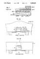
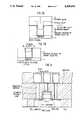
- FIG. 1is taken from Dalton and shows that multilayer devices produced by traditional processing schemes have seams in the dielectric layers at the location of the metal conductor lines and have a very irregular top surface.
- Planarityis in part dependent on the pattern density, and non-planar surfaces result in puddling problems during subsequent metalization. If an RIE technique is used on polyimide, an etch stop is needed for removal of photoresist on top of aluminum or copper based lines when the lines are etched down to the polyimide surface because the photoresist removal process would also remove polyimide. RIE of any high copper content, aluminum or copper alloy is extremely difficult. A serious drawback of traditional processes which include metal RIE is that a large number of metal shorts tend to develop with fine geometry due to particle defects.
- U.S. Pat. No. 4,824,802 to Brown et al.discloses a method for filling interlevel dielectric vias or contact holes in multilevel VLSI metalization structures.
- an intermediary metalsuch as tungsten or molybdenum is either selectively deposited in openings in an insulator or non-selectively deposited over the entire surface and in the openings of the insulator by CVD, then a planarization resist, such as azoquinonenovolac-type resists, polymethacrylates, polyimides, or other thermoplastic materials, is applied over the top of the intermediary metal.
- a planarized structureis then obtained by etching to a level where the intermediary metal is even with the resist.
- U.S. Pat. No. 4,944,836 to Beyer et al.discloses a chemical-mechanical polishing technique which can be used to produce coplanar metal/insulator films on a substrate.
- Beyer et al.contemplate patterning an underlying insulating layer, depositing an Al-Cu film, and then using a chemical-mechanical polishing technique wherein an alumina slurry in dilute nitric acid is mechanically rubbed on the surface to remove Al-Cu.
- the polishing compoundtends to have a significantly higher removal rate for Al-Cu than the underlying insulator.
- the resulting structureincludes Al-Cu lines planarized with the insulating layer, and subsequent layers can easily be added in the fabrication of multilayer structures.
- U.S. Pat. No. 4,956,313 to Cote et al.discloses a via filling and planarization technique wherein Al-Cu alloy lines are patterned on top of a first passivation layer on a substrate, the lines are overcoated with a second passivation layer which is preferably a doped glass such as phosphosilicate glass (PSG) or borophosphosilicate glass (BPSG) which conforms over the contours of the Al-Cu alloy lines, vias are then formed in the second passivation layer to expose the lines, and tungsten is applied over the surface of the second passivation layer and in the vias by CVD. It is reported in Cote et al. that CVD tungsten is conformal in character and can fill the vias without creating voids. The structure is then planarized by polishing with an abrasive slurry.
- a second passivation layerwhich is preferably a doped glass such as phosphosilicate glass (PSG) or borophosphos
- Rossnagel et al. J. Vac. Sci. Technol. 2:261discloses a collimated magnetron sputter deposition technique for depositing films that are compatible with lift-off patterning techniques and hole filling.
- the techniqueis also presented in U.S. Pat. No. 4,824,544 which is herein incorporated by reference.
- Shiozaki et al.Abstracts of the 19th Conference on Solid State Devices and Materials, discloses the use of selective tungsten deposition for hole filling on top of a high resistivity hard metal such as MoSi x and is unrelated to encapsulation of a soft metal.
- It is still another object of this invention to provide a method for promoting adhesion of CVD tungsten in high aspect ratio vias or interconnect lineswhich includes providing a liner in the vias or interconnect lines formed from a refractory metal, or alloys or compounds thereof, prior to CVD tungsten.
- a simple and cost effective techniquewhich results in electrical conductors that are corrosion-free and exhibit resistance to wear and electromigration, and has demonstrated high process yield.
- this techniqueavoids cumbersome dielectric planarization steps completely as the deposition takes place only on the planar surfaces to start with.
- the techniqueuses ordinary batch or single wafer PVD processes such as evaporation, sputtering or collimated sputtering followed by a conformal deposition of refractory metal.
- FIG. 1is a cross-sectional side view of a prior art semiconductor substrate showing an uneven top surface
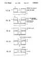
- FIGS. 2A through 2Eare sequential cross-sectional side views of a semiconductor substrate illustrating one variation of the invention.
- FIGS. 3A and 3Bare sequential cross-sectional side views of a substrate with a device thereon overcoated by an insulator being planarized prior to patterning the insulator;
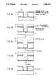
- FIGS. 4A through 4Eare sequential cross-sectional side views of a semiconductor substrate illustrating another variation of the invention.
- FIG. 5A through 5Eare sequential cross-sectional side views of a semiconductor substrate illustrating still another variation of the invention.
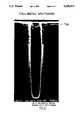
- FIG. 6is a scanning electron micrograph (SEM) of a liner deposited in a via using PVD
- FIGS. 7A and 7Bare sequential cross-sectional side views of a semiconductor substrate illustrating yet another variation of the invention.
- FIG. 8is a cross-sectional view of an exemplary, multilevel, damascene structure wherein PVD Al x Cu y alloy is capped with CVD tungsten;
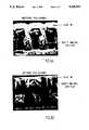
- FIGS. 9A and 9Bare cross-sectional SEM micrographs of structures with tungsten capped Al-Cu alloy lines prior to and after chemical-mechanical polishing, respectively.
- the inventionis generally related to methods for forming metal filled vias and conductor lines on a substrate where the vias and conductor lines include a soft, low resistivity metal which is capped with a relatively hard, refractory metal which is resistant to corrosion, wear, and electromigration, and where the vias and conductor lines are planar with a dielectric layer coated on the substrate.
- the vias and conductor linesinclude a soft, low resistivity metal which is capped with a relatively hard, refractory metal which is resistant to corrosion, wear, and electromigration, and where the vias and conductor lines are planar with a dielectric layer coated on the substrate.
- 2A-E and 5A-Ecan be used as well as single layers of inorganic or organic insulator materials).
- the inventionis not restricted to any particular metal combinations; rather, an objective of the invention is to overlay a soft, low resistance metal or metal alloy with a hard refractory metal which can withstand wear, corrosion and electromigration.
- the inventionhas particular relevance to electrical systems which use aluminum and copper alloys since it has been discovered that uniform, conformal coatings of a refractory metal liner material can be deposited in submicron vias and trenches with reliable high aspect ratio filling using PVD collimated sputtering.
- the refractory metal linerwill serve as an effective diffusion barrier to copper for subsequent processing.
- a substrate 10is first overcoated with a dielectric which is subsequently patterned.
- the substrate 10is preferably silicon, gallium arsenide, or some other material which is suitable for making integrated circuits.
- the substrate 10may be a ceramic, glass, or composite material commonly used for packaging semiconductors and for making thin film interconnections.
- the substrate 10preferably has a plurality of semiconductor devices formed therein which may include field effect transistors (FETs), bipolar transistors, resistors, Schottky diodes, or the like.
- FETsfield effect transistors
- bipolar transistorsbipolar transistors
- resistorsresistors
- Schottky diodesSchottky diodes
- the dielectric composite shown in FIG. 2Aincludes top and bottom inorganic dielectric layers 13 and 11, respectively, which may be silicon dioxide (SiO 2 ), silicon nitride (Si 3 N 4 ), or the like.
- the inorganic layers 11 and 13are both preferably deposited using plasma enhanced chemical vapor deposition (PECVD) where SiO 2 is first deposited at 90 Torr on the conducting substrate 10 and Si 3 N 4 (0.075 to 0.1 ⁇ m) is provided as a barrier against mobile ion diffusion.
- PECVDplasma enhanced chemical vapor deposition
- a thicker organic dielectric layer 12such as a polyimide, is deposited between the inorganic layers 11 and 13.
- a single layer of an inorganic dielectricsuch as SiO 2 , PSG, or BPSG, or an organic dielectric, such as polyimide, may also be employed and may be deposited by any of a number of well known techniques such as by growing in an oxidative atmosphere, sputtering, or PECVD. While FIGS. 2A-E and 5A-E show the use of the composite structure and FIGS.
- 3A-B, 4A-E, and 7A-Bshow the use of a single inorganic or dielectric layer, it should be understood that the dielectric layer is not limiting to the practice of this invention and that any dielectric (e.g., inorganic or organic) used by itself or in combination could be employed in the practice of this invention.
- any dielectrice.g., inorganic or organic
- FIG. 2Ashows an opening 14 formed in the dielectric composite, and this opening may be a via or a trench for a conductive line.
- the substrate 10is likely to have several hundred to thousands of openings 14 like that shown in FIG. 2A where the resulting dense, complex pattern will ultimately interconnect circuits on or in the substrate.
- the openings 14are preferably formed using contrast enhanced lithography (CEL) followed by trench or hole etching with a multiwafer tool using CHF 3 and O 2 with an optimum overetch to ensure that the opening 14 has the desired dimensions and extends to a contact on the surface of the substrate 10 for a via stud pattern.
- the dielectric layersare preferably partially etched to a depth about 10% higher than the metal thickness to be employed.
- the insulator 20 coated over the device 18should first be planarized before an opening 22 is created. Planarization can be achieved by RIE, chemical-mechanical polishing, a combination of both RIE and chemical-mechanical polishing, or by other means.
- FIGS. 2B-2Eillustrate a first variation of the present invention wherein a planar patterned structure, which can be either the one shown in FIG. 2A or the one shown in FIG. 3B or any other structure which has an opening 14 formed in an overcoated dielectric, then has a refractory metal layer 15 deposited over the inorganic dielectric layer 13 and on the exposed substrate 10 at the bottom of gap 14.
- a planar patterned structurewhich can be either the one shown in FIG. 2A or the one shown in FIG. 3B or any other structure which has an opening 14 formed in an overcoated dielectric
- a refractory metal layer 15deposited over the inorganic dielectric layer 13 and on the exposed substrate 10 at the bottom of gap 14.
- PVD collimated sputteringsimilar to that described in U.S. Pat. No. 4,824,544, can be used in the practice of the invention, but that collimated sputtering produces a conformal layer which would coat the side walls of opening 14, contrary to that which is shown in FIG. 2B.
- the use of collimated sputtering to create a refractory metal lineris discussed in more detail below.
- the refractory metalmay be titanium (Ti), titanium alloys or compounds such as Ti/TiN, tungsten (W), titanium/tungsten (Ti/W) alloys, or chromium (Cr) or tantalum (Ta) and their alloys, or some other suitable material. If copper based lines or vias are to be formed, a refractory metal should be used which can act as a diffusion barrier to copper such that diffusion during subsequent processing of deposited copper in the opening 14 into the substrate 10 is prevented.
- a single, binary or ternary metalization 16is deposited over the refractory metal 15 by PVD using evaporation. Again, since evaporation is used, the side walls of opening 14 are not coated. However, it should be understood that the metalization 16 could be applied by collimated sputtering, in which case a conformal coating of the metalization within the opening 14 and on top of the dielectric stack.
- the metalizationis Al x Cu y , where the sum of x and y is equal to one and both x and y are greater than or equal to zero and less than or equal to one; however, ternary alloys such as Al-Pd-Cu and multicomponent alloys such as Al-Pd-Nb-Au would also be suitable.
- the principal characteristic of the metalization 16is that it is a low resistivity and soft material compared to the refractory metal 15.
- the opening 14, which represents the line pattern or interlevel via patternis filled with the metalization 16 to a depth of 100 to 400 nm below the surface of the line or via. It should be understood that the metalization 16 shown in FIGS. 4A-E, 5A-E, and 7A-B would be of the same sort described above.
- FIG. 2Cshows a refractory metal 17, such as tungsten, cobalt, nickel, molybdenum, or alloys/compounds such as Ti/TiN, deposited over the structure.
- Deposition of the refractory metal 17may be by one step CVD or by a two step process, as is best explained in FIGS. 4a-e, wherein the first step involves collimated sputtering or the like of an adhesion promoting compound such as titanium or titanium nitride to create a conformal blanket coating, and the second step includes depositing a thin CVD layer of tungsten to achieve a higher degree of conformality.
- CVD deposition of the refractory metalis preferably achieved with SiH 4 or H 2 reduction of WF 6 .
- a particularly preferred CVD procedureinvolves SiH 4 reduction of WF 6 followed by H 2 reduction of WF 6 because, on top of a TiN layer, CVD of tungsten proceeds smoothly with SiH 4 reduction of WF 6 , but not with H 2 reduction.
- the refractory metal 17provides a wear resistant, corrosion resistant, and electromigration resistant coating to the underlying soft, low resistivity metalization 16 in opening 14.
- a particularly good advantage to using CVD with SiH 4 reduction of WF 6is that the ratio of SiH 4 to WF 6 can be varied to incorporate different amounts of silicon into the tungsten to achieve beneficial properties.
- the refractory metal 17it would be preferable to deposit the refractory metal 17 at a 0.5 SiH 4 to WF 6 ratio while the opening 14 in the dielectric is being filled since so doing will result in a lower resistance refractory metal; however, towards the top surface of the dielectric to deposit at a 2.0 SiH 4 to WF 6 ratio is preferable since this will result in more silicon incorporation which has greater wear resistance.
- the silicon doped tungstencan be used as a wear resistant coating or a polishing stop (e.g., it will be more resistant to an alumina slurry in ferric nitrate used in chemical-mechanical polishing).
- the CVD applied refractory metal 17creates tapering side walls around the metalization 16 and the metalization 16 becomes completely encapsulated in refractory metal 17 and underlying refractory metal 15.
- FIGS. 2D and 2Eshow that the structure is planarized after the CVD application of the refractory metal 17 to yield a structure wherein a two part conductive via or line, which includes a central, soft, low resistivity metalization 16, encapsulated in a hard, wear resistant refractory metal 17, has a top surface which is even with the top surface of the dielectric composite on substrate 10.
- Planarizationcan be accomplished in one or two steps by chemical-mechanical polishing with a slurry such as alumina in dilute ferric nitrate or by RIE in the presence of SF 6 or Cl 2 based chemistry. If chemical-mechanical polishing is employed, slurries can be selected to remove different metal layers on the stack.
- Ti/TiN/W on top of coppercan be removed using the alumina in dilute ferric nitrate slurry, and then the remaining copper can be removed by switching to a slurry without alumina.
- Combinations of RIE removal of the refractory metal layer 17 followed by chemical-mechanical polishing of the remaining metalization 16 and remaining refractory metal 17 above the top organic or inorganic layer 13are also contemplated.
- a particular planarization procedure contemplatedincludes removing tungsten refractory metal 17 by either chemical-mechanical polishing or RIE with SF 6 or Cl 2 based chemistry down to an Al-Cu alloy metalization 16 surface as shown in FIG.
- the Al-Cu CVD layeris etched down to the inorganic layer 13 surface, and finally, the remaining tungsten 17 on the dielectric surface is either polished, wet etched or RIE etched in Cl 2 to yield the structure shown in FIG. 2E.
- FIGS. 4A through 4Eshow another variation on the invention where like elements to those identified above are indicated by the same numerals in each of the Figures.
- copper metalization 16is deposited in an opening 14 created in an inorganic or organic dielectric 15 formed on substrate 10.
- a thin layer of refractory metal 24such as titanium, titanium nitride (TiN), tungsten, tantalum, or alloys and compounds thereof, is deposited over the inorganic or organic dielectric 15 surface and inside the opening 14 via collimated sputtering.
- collimated sputteringis generally described in U.S. Pat. No. 4,824,544 to Rossnagel et al. where a lift-off procedure is discussed.
- the aspect ratiogenerally refers to the ratio of the height of a trench or via relative to its width in the case of a trench or its diameter in the case of a via.
- Trenches and vias with aspect ratios greater than twoare generally considered to have a high aspect ratio.
- scatteringtends to dominate above pressures of 1 mTorr (preferably around 3 mTorr), while directional deposition dominates below 1 mTorr.
- Collimated sputteringis described in more detail below in conjunction with FIGS. 5A-E and 6.
- Completely coating the bottom surface and side walls of opening 14 with a refractory metal layer 24, as shown in FIG. 4a,is especially important when a copper based alloy metalization 16 is used since copper will diffuse into the substrate 10 during subsequent high temperature processing and ruin the device if no diffusion barrier is provided.
- the copper metalization 16can be deposited by PVD using either evaporation or collimated sputtering or by other techniques. When submicron, high aspect ratio holes are to be filled, prior art CVD techniques have been unsuccessful for filling the holes with aluminum and copper based alloys; therefore, the preferred method for filling is by PVD techniques.
- a thin layer 26 of titanium, Ti/TiN, tantalum or chromiumis then applied over the copper metalization 16 surface to promote adhesion.
- a refractory metalsuch as tungsten is then deposited by CVD by SiH 4 or H 2 reduction of WF 6 to yield the structure shown in FIG. 4B.
- varying the SiH 4 to WF 6 ratio during CVDcan advantageously be used to make a harder, more wear resistant, tungsten with incorporated silicon layer near the top surface of the dielectric 15.
- the interfacial thin layer 26should be chosen so that it does not attack the underlying copper metalization 16.
- FIG. 4cshows that first tungsten is planarized by polishing or by RIE and FIG. 4d shows that copper is selectively removed by wet etching.
- a wet etch solutionbased on hydrogen peroxide (H 2 O 2 ) and hydrogen tetroxide (H 2 O 4 ) to planarize the copper.
- H 2 O 2hydrogen peroxide
- H 2 O 4hydrogen tetroxide
- the tungsten 17can be selectively removed by RIE, polishing or other techniques.
- a preferred method for removing the tungsten refractory metal 17 which projects above the dielectric 15 surfaceis by chemical-mechanical polishing using an alumina in ferric nitrate slurry or the like. Because tungsten is a relatively hard material, it does not scratch or corrode when subjected to chemical-mechanical polishing. Rather than the three step approach discussed above, it may be preferable to remove the tungsten refractory metal 17, the thin layer 26 adhesion promoter, and the copper metalization 16 located above the surface of the insulator 15 in one step using chemical-mechanical polishing.
- FIGS. 5A through 5Eshow yet another variation on the invention where like numerals indicate like elements.
- FIG. 5Ashows a refractory metal liner 28 is deposited in the opening 14 prior to metalization in a fully or partially conformal manner using collimated sputtering like that described in Rossnagel et al. J. Vac. Sci. Technol. 2:261 (March/April 1991) and U.S. Pat. No. 4,824,544 to Rossnagel et al. which are herein incorporated by reference.
- collimated sputteringrefractory metal atoms are passed through a honeycomb like structure with an aspect ratio of depth to area of greater than one at pressures greater than 0.5 mTorr. Table 1 presents conditions which have been used for liner deposition.
- providing a conformal layer of TiN or other suitable materialswill provide an effective diffusion barrier for copper based alloys.
- scattering depositiondominates (e.g., above 1 mTorr) rather than at lower pressures where directional deposition dominates.
- FIG. 6presents an SEM micrograph of a refractory metal liner in a via created by PVD collimated sputtering as described above.
- FIG. 6shows that complete coverage of the bottom and sidewalls of the via can be obtained.
- N 2 plasmawas used along with argon in the presence of a titanium target.
- the linercan improve adhesion and prevent any attack of CVD tungsten on the underlying substrate.
- the conformality of a linerincrease when the aspect ratio of the collimator increases.
- a robust liner which can serve as a diffusion barrieris required.
- Low pressure collimation of a refractory linere.g., Ta, Ti/TiN, or Ti/W, etc.
- a two step collimation processwas employed. Specifically, in the first step, a thin liner was deposited using a pressure below 0.8 mT to get bottom coverage of more than 60%, and in the second step, the pressure was increased in-situ to 3 to 4 mT to get a dense microstructure on the sidewall using the same collimator.
- FIGS. 5B-Eshow similar steps to those shown in FIGS. 2B-E and FIGS. 4A-E are performed in another variation on the invention.
- FIG. 5Bshows that an adhesion promoter layer 26, such as Ti, Cr, Ta, Ti/W, or the like, is deposited by PVD evaporation over the top of the refractory metal liner and in the bottom of the gap 14.
- FIG. 5Bshows Al-Cu alloy or other metalization 16 being deposited by PVD evaporation techniques to a level 100 to 400 nm below the surface of the dielectric.
- 5C-Erespectively show deposition of a conformal layer of tungsten or other refractory material to cap the low resistivity metalization 16, planarizing the tungsten by RIE or polishing, or the like, and planarizing the structure using the two step wet etching of the aluminum-copper alloy with H 2 O 2 followed by chemical-mechanical polishing of tungsten as shown in FIGS. 4c and 4d or simply planarizing by one step RIE or chemical-mechanical polishing.
- a slurry similar to that used for tungsten polishingcan be used.
- the structure shown in FIG. 5Ehas a CVD refractory metal 17 encapsulating a low resistivity metalization 16 where there is a tapered refractory metal 17 region.
- FIGS. 7A and 7Bshow yet another variation on the invention where like elements are indicated by like numerals.
- both a conformal, preferably refractory metal, liner/diffusion barrier 28 and a conformal Al x Cu y or other suitable, low resistivity alloy or metalization 16 layerare deposited in the opening in the organic or inorganic dielectric 15 on substrate 10 using PVD collimated sputtering procedures.
- a refractory metal 17 capping layersuch as tungsten, titanium, tantalum, or the like, is deposited by CVD to blanket coat the structure.
- FIG. 7Bshows that the structure is then planarized using RIE, chemical-mechanical polishing, or by other techniques.
- FIG. 8shows an example of one multilevel semiconductor device which includes a top surface having tungsten capped Al x Cu y alloy lines flush with the top most insulator layer.
- the vias or trenches with CVD tungstenpreferably include a TiN liner formed by collimated sputtering to promote adhesion.
- Many other semiconductor devicescan be fabricated within the practice of this invention.
- FIGS. 9a and 9bare SEM micrographs of a cross-section of a semiconductor device.
- FIG. 9ashows separated SiO 2 portions projecting up from a silicon surface with Al-Cu alloy between and on top of the SiO 2 . Between and on top of the Al-Cu alloy is a CVD tungsten layer.
- FIG. 9arepresents a structure with capped lines prior to polishing.
- FIG. 9bshows an SEM micrograph of the cross-section of a multilayer structure after chemical-mechanical polishing has removed the tungsten and Al-Cu alloy above the top surface of the SiO 2 projections.
Landscapes
- Engineering & Computer Science (AREA)
- Physics & Mathematics (AREA)
- Condensed Matter Physics & Semiconductors (AREA)
- General Physics & Mathematics (AREA)
- Computer Hardware Design (AREA)
- Microelectronics & Electronic Packaging (AREA)
- Power Engineering (AREA)
- Manufacturing & Machinery (AREA)
- Internal Circuitry In Semiconductor Integrated Circuit Devices (AREA)
- Physical Vapour Deposition (AREA)
- Electrodes Of Semiconductors (AREA)
Abstract
Description
WF.sub.6 +2Al→2AlF.sub.3 +W Eq. 1
TABLE 1 ______________________________________ DEPOSITION OF LINER BY COLLIMATION BOTTOM/ STEP COVERAGE TOP ASPECT RATIO SIDEWALL/TOP (%) (%) ______________________________________ 1:1 38 60 1:2 39 70 1:4 42 100 NO COLLIMATION 0 10 12 ______________________________________
TABLE 2 ______________________________________ LINE RESISTANCE OF TUNGSTEN CAPPED LOW RESISTIVITY METAL AFTER POLISHING.sup.a Resistance Resistance Structure before W dep. after W dep. Yield ______________________________________ (A) CREATED USING EVAPORATION.sup.b Ti(20nm)/TiN(35nm)/ 0.042 0.04 95% Al-Cu(800nm)/ W(200nm) Ti(20nm)/Al-Cu(800nm)/ 0.042 0.052 95% W(200nm) Ti(20nm)/Al-Cu(800nm)/ 0.042 0.054 94% Ti(20nm)/W(200nm) Ti(20nm)/TiN(25nm)/ 0.025 0.023 97% CVD W(30nm)/ Al-Cu(1300nm)/ W(200nm) Ti(50nm)/TiN(25nm)/ 0.025 0.032 96% Ti(20nm)/Al-Cu(1300nm)/ Ti(20nm)/TiN(20nm)/ W(200nm) Ti(50nm)/TiN(50nm)/ 0.023 0.021 100% Ti(50nm)/Al-Cu(600nm)/ Ti(20nm)/Cu(700nm)/ Ti(20nm)/TiN(20nm)/ CVD W(200nm) (B) CREATED USING COLLIMATED SPUTTERING.sup.c Ti(20nm)/TiN(35nm)/ 0.042 0.04 84% Al-Cu(800nm)/ CVD W(200nm) Ti(20nm)/Al-Cu(800nm)/ 0.042 0.05 81% CVD W(200nm) Ti(20nm)/W(20nm)/ 0.040 0.039 85% Al-Cu(800nm)/ CVD W(200nm) Ti(20nm)/TiN(75nm)/ 0.024 0.022 80% Cu(800nm)/Ti(20nm)/ TiN(25nm)/ CVD W(200nm) (C) CREATED USING SPUTTERING WITHOUT COLLIMATION.sup.d Ti(20nm)/TiN(35nm)/ 0.040 0.04 86% Al-Cu(800nm)/ CVD W(200nm) ______________________________________ .sup.a In all the exeriments, the line lengths varied from 13.5 to 50 cm with an area of the chip close to 1.6 mm.sup.2. The metal pitches varied from 1 μm to 2 μm The aspect ratio of the holes filled were from 2 to 8 and for lines, 2 to 4. .sup.b In the Evaporation Experiments, Ti/TiN bilayers were deposited by collimation sputtering. .sup.c Colimation aspect ratio of 1:1. .sup.d Sputtering pressure ranged between 0.5 to 0.8mTorr.
Claims (9)
Priority Applications (33)
| Application Number | Priority Date | Filing Date | Title |
|---|---|---|---|
| US07/841,967US5300813A (en) | 1992-02-26 | 1992-02-26 | Refractory metal capped low resistivity metal conductor lines and vias |
| US07/928,335US5403779A (en) | 1992-02-26 | 1992-08-12 | Refractory metal capped low resistivity metal conductor lines and vias formed using PVD and CVD |
| KR1019930000764AKR0128264B1 (en) | 1992-02-26 | 1993-01-21 | Method of forming semiconductor devices, liners and metal wires and vias |
| EP93101519AEP0561132B1 (en) | 1992-02-26 | 1993-02-01 | Method of forming a conformal refractory metal layer in a submicron opening |
| DE69332917TDE69332917T2 (en) | 1992-02-26 | 1993-02-01 | Metal conductor tracks and through lines of low resistance covered with fire-resistant metal made of PVD and CVD |
| SG1997004072ASG70045A1 (en) | 1992-02-26 | 1993-02-01 | Refractory metal capped low resistivity metal conductor lines and vias formed using pvd and cvd |
| SG1997004069ASG70043A1 (en) | 1992-02-26 | 1993-02-01 | Refractory metal capped low resistivity metal conductor lines and vias formed using pvd and cvd |
| SG200105658ASG115407A1 (en) | 1992-02-26 | 1993-02-01 | Refractory metal capped low resistivity metal conductor lines and vias using pvd and cvd |
| DE69333604TDE69333604T2 (en) | 1992-02-26 | 1993-02-01 | PVD and DVD formed refractory metal covered metal traces and low resistivity through holes |
| EP97105003AEP0788156B1 (en) | 1992-02-26 | 1993-02-01 | Refractory metal capped low resistivity metal conductor lines and vias formed using PVD and CVD |
| SG1997004071ASG70044A1 (en) | 1992-02-26 | 1993-02-01 | Refractory metal capped low resistivity metal conductor lines and vias formed using pvd and cvd |
| DE69329663TDE69329663T2 (en) | 1992-02-26 | 1993-02-01 | Process for making a compliant refractory metal layer in a submicron opening |
| SG200105657ASG105511A1 (en) | 1992-02-26 | 1993-02-01 | Refractory metal capped low resistivity metal conductor lines and vias formed using pvd and cvd |
| EP99112665AEP0966037B1 (en) | 1992-02-26 | 1993-02-01 | Refractory metal capped low resistivity metal conductor lines and vias formed using PVD and CVD |
| SG1997004075ASG70046A1 (en) | 1992-02-26 | 1993-02-01 | Refractory metal capped low resistivity metal conductor lines and vias formed using pvd and cvd |
| SG200201110ASG111047A1 (en) | 1992-02-26 | 1993-02-01 | Refractory metal capped low resistivity metal conductor lines and vias formed using pvd and cvd |
| SG1996000500ASG44450A1 (en) | 1992-02-26 | 1993-02-01 | Refractory metal capped low resistivity metal conductor lines and vias formed using pvd and cvd |
| JP5028812AJP2516307B2 (en) | 1992-02-26 | 1993-02-18 | Low-resistivity conductor structure capped with refractory metal and method of forming the same |
| CN93101333ACN1044649C (en) | 1992-02-26 | 1993-02-24 | Refractory metal covered low resistance metal conductor lines and vias and method of manufacture |
| TW082103470ATW291576B (en) | 1992-02-26 | 1993-05-04 | |
| US08/125,107US5426330A (en) | 1992-02-26 | 1993-09-21 | Refractory metal capped low resistivity metal conductor lines and vias |
| CN94115341ACN1081390C (en) | 1992-02-26 | 1994-09-15 | Refractory metal capped low resistivity metal conductor lines and vias formed using PVD and CVD |
| US08/346,208US5585673A (en) | 1992-02-26 | 1994-11-22 | Refractory metal capped low resistivity metal conductor lines and vias |
| US08/753,991US5889328A (en) | 1992-02-26 | 1996-12-03 | Refractory metal capped low resistivity metal conductor lines and vias |
| KR1019970002511AKR0134121B1 (en) | 1992-02-26 | 1997-01-28 | Semiconductor device |
| KR1019970002512AKR0134120B1 (en) | 1992-02-26 | 1997-01-28 | Semiconductor device |
| KR1019970002510AKR0134122B1 (en) | 1992-02-26 | 1997-01-28 | Semiconductor devices |
| CN97119556ACN1112730C (en) | 1992-02-26 | 1997-09-25 | Refractory metal capped low resistivity metal conductor lines and vias formed using PVD and CVD |
| CN97119558ACN1111908C (en) | 1992-02-26 | 1997-09-25 | Semiconductor device |
| CNB971195579ACN1150597C (en) | 1992-02-26 | 1997-09-25 | Method for forming liners in submicron holes and lines with large aspect ratios |
| US09/113,917US5976975A (en) | 1992-02-26 | 1998-07-10 | Refractory metal capped low resistivity metal conductor lines and vias |
| US09/113,918US6147402A (en) | 1992-02-26 | 1998-07-10 | Refractory metal capped low resistivity metal conductor lines and vias |
| US09/113,916US6323554B1 (en) | 1992-02-26 | 1998-07-10 | Refractory metal capped low resistivity metal conductor lines and vias formed using PVD and CVD |
Applications Claiming Priority (1)
| Application Number | Priority Date | Filing Date | Title |
|---|---|---|---|
| US07/841,967US5300813A (en) | 1992-02-26 | 1992-02-26 | Refractory metal capped low resistivity metal conductor lines and vias |
Related Parent Applications (1)
| Application Number | Title | Priority Date | Filing Date |
|---|---|---|---|
| US07/928,335DivisionUS5403779A (en) | 1992-02-26 | 1992-08-12 | Refractory metal capped low resistivity metal conductor lines and vias formed using PVD and CVD |
Related Child Applications (2)
| Application Number | Title | Priority Date | Filing Date |
|---|---|---|---|
| US07/928,335DivisionUS5403779A (en) | 1992-02-26 | 1992-08-12 | Refractory metal capped low resistivity metal conductor lines and vias formed using PVD and CVD |
| US08/125,107ContinuationUS5426330A (en) | 1992-02-26 | 1993-09-21 | Refractory metal capped low resistivity metal conductor lines and vias |
Publications (1)
| Publication Number | Publication Date |
|---|---|
| US5300813Atrue US5300813A (en) | 1994-04-05 |
Family
ID=25286205
Family Applications (8)
| Application Number | Title | Priority Date | Filing Date |
|---|---|---|---|
| US07/841,967Expired - LifetimeUS5300813A (en) | 1992-02-26 | 1992-02-26 | Refractory metal capped low resistivity metal conductor lines and vias |
| US07/928,335Expired - LifetimeUS5403779A (en) | 1992-02-26 | 1992-08-12 | Refractory metal capped low resistivity metal conductor lines and vias formed using PVD and CVD |
| US08/125,107Expired - LifetimeUS5426330A (en) | 1992-02-26 | 1993-09-21 | Refractory metal capped low resistivity metal conductor lines and vias |
| US08/346,208Expired - LifetimeUS5585673A (en) | 1992-02-26 | 1994-11-22 | Refractory metal capped low resistivity metal conductor lines and vias |
| US08/753,991Expired - LifetimeUS5889328A (en) | 1992-02-26 | 1996-12-03 | Refractory metal capped low resistivity metal conductor lines and vias |
| US09/113,918Expired - Fee RelatedUS6147402A (en) | 1992-02-26 | 1998-07-10 | Refractory metal capped low resistivity metal conductor lines and vias |
| US09/113,916Expired - LifetimeUS6323554B1 (en) | 1992-02-26 | 1998-07-10 | Refractory metal capped low resistivity metal conductor lines and vias formed using PVD and CVD |
| US09/113,917Expired - LifetimeUS5976975A (en) | 1992-02-26 | 1998-07-10 | Refractory metal capped low resistivity metal conductor lines and vias |
Family Applications After (7)
| Application Number | Title | Priority Date | Filing Date |
|---|---|---|---|
| US07/928,335Expired - LifetimeUS5403779A (en) | 1992-02-26 | 1992-08-12 | Refractory metal capped low resistivity metal conductor lines and vias formed using PVD and CVD |
| US08/125,107Expired - LifetimeUS5426330A (en) | 1992-02-26 | 1993-09-21 | Refractory metal capped low resistivity metal conductor lines and vias |
| US08/346,208Expired - LifetimeUS5585673A (en) | 1992-02-26 | 1994-11-22 | Refractory metal capped low resistivity metal conductor lines and vias |
| US08/753,991Expired - LifetimeUS5889328A (en) | 1992-02-26 | 1996-12-03 | Refractory metal capped low resistivity metal conductor lines and vias |
| US09/113,918Expired - Fee RelatedUS6147402A (en) | 1992-02-26 | 1998-07-10 | Refractory metal capped low resistivity metal conductor lines and vias |
| US09/113,916Expired - LifetimeUS6323554B1 (en) | 1992-02-26 | 1998-07-10 | Refractory metal capped low resistivity metal conductor lines and vias formed using PVD and CVD |
| US09/113,917Expired - LifetimeUS5976975A (en) | 1992-02-26 | 1998-07-10 | Refractory metal capped low resistivity metal conductor lines and vias |
Country Status (8)
| Country | Link |
|---|---|
| US (8) | US5300813A (en) |
| EP (3) | EP0966037B1 (en) |
| JP (1) | JP2516307B2 (en) |
| KR (4) | KR0128264B1 (en) |
| CN (5) | CN1044649C (en) |
| DE (3) | DE69332917T2 (en) |
| SG (8) | SG115407A1 (en) |
| TW (1) | TW291576B (en) |
Cited By (103)
| Publication number | Priority date | Publication date | Assignee | Title |
|---|---|---|---|---|
| US5412250A (en)* | 1993-09-24 | 1995-05-02 | Vlsi Technology, Inc. | Barrier enhancement at the salicide layer |
| US5426330A (en)* | 1992-02-26 | 1995-06-20 | International Business Machines Corporation | Refractory metal capped low resistivity metal conductor lines and vias |
| US5430328A (en)* | 1994-05-31 | 1995-07-04 | United Microelectronics Corporation | Process for self-align contact |
| US5565383A (en)* | 1993-12-03 | 1996-10-15 | Nec Corporation | Method for selective formation of silicide films without formation on vertical gate sidewalls using collimated sputtering |
| US5592024A (en)* | 1993-10-29 | 1997-01-07 | Kabushiki Kaisha Toshiba | Semiconductor device having a wiring layer with a barrier layer |
| US5602423A (en)* | 1994-11-01 | 1997-02-11 | Texas Instruments Incorporated | Damascene conductors with embedded pillars |
| US5612254A (en)* | 1992-06-29 | 1997-03-18 | Intel Corporation | Methods of forming an interconnect on a semiconductor substrate |
| US5731634A (en)* | 1992-07-31 | 1998-03-24 | Kabushiki Kaisha Toshiba | Semiconductor device having a metal film formed in a groove in an insulating film |
| US5731245A (en)* | 1994-08-05 | 1998-03-24 | International Business Machines Corp. | High aspect ratio low resistivity lines/vias with a tungsten-germanium alloy hard cap |
| US5739579A (en)* | 1992-06-29 | 1998-04-14 | Intel Corporation | Method for forming interconnections for semiconductor fabrication and semiconductor device having such interconnections |
| US5747879A (en)* | 1995-09-29 | 1998-05-05 | Intel Corporation | Interface between titanium and aluminum-alloy in metal stack for integrated circuit |
| US5849367A (en)* | 1996-12-11 | 1998-12-15 | Texas Instruments Incorporated | Elemental titanium-free liner and fabrication process for inter-metal connections |
| US5942767A (en)* | 1995-11-21 | 1999-08-24 | Samsung Electronics Co., Ltd. | Thin film transistors including silicide layer and multilayer conductive electrodes |
| US5952874A (en)* | 1994-12-30 | 1999-09-14 | Consorzio Per La Ricerca Sulla Microeletrronica Nel Mezzogiorno | Threshold extracting method and circuit using the same |
| US5965459A (en)* | 1996-10-11 | 1999-10-12 | International Business Machines Corporation | Method for removing crevices induced by chemical-mechanical polishing |
| US5990011A (en)* | 1997-09-18 | 1999-11-23 | Micron Technology, Inc. | Titanium aluminum alloy wetting layer for improved aluminum filling of damescene trenches |
| US5993686A (en)* | 1996-06-06 | 1999-11-30 | Cabot Corporation | Fluoride additive containing chemical mechanical polishing slurry and method for use of same |
| US6048787A (en)* | 1998-09-08 | 2000-04-11 | Winbond Electronics Corp. | Borderless contacts for dual-damascene interconnect process |
| US6069068A (en)* | 1997-05-30 | 2000-05-30 | International Business Machines Corporation | Sub-quarter-micron copper interconnections with improved electromigration resistance and reduced defect sensitivity |
| US6080655A (en)* | 1997-08-21 | 2000-06-27 | Micron Technology, Inc. | Method for fabricating conductive components in microelectronic devices and substrate structures thereof |
| US6096576A (en)* | 1997-09-02 | 2000-08-01 | Silicon Light Machines | Method of producing an electrical interface to an integrated circuit device having high density I/O count |
| US6096632A (en)* | 1997-04-11 | 2000-08-01 | Nec Corporation | Fabrication method of semiconductor device using CMP process |
| US6111301A (en)* | 1998-04-24 | 2000-08-29 | International Business Machines Corporation | Interconnection with integrated corrosion stop |
| US6114243A (en)* | 1999-11-15 | 2000-09-05 | Chartered Semiconductor Manufacturing Ltd | Method to avoid copper contamination on the sidewall of a via or a dual damascene structure |
| US6127276A (en)* | 1998-06-02 | 2000-10-03 | United Microelectronics Corp | Method of formation for a via opening |
| US6130161A (en)* | 1997-05-30 | 2000-10-10 | International Business Machines Corporation | Method of forming copper interconnections with enhanced electromigration resistance and reduced defect sensitivity |
| US6153521A (en)* | 1998-06-04 | 2000-11-28 | Advanced Micro Devices, Inc. | Metallized interconnection structure and method of making the same |
| US6157081A (en)* | 1999-03-10 | 2000-12-05 | Advanced Micro Devices, Inc. | High-reliability damascene interconnect formation for semiconductor fabrication |
| US6162729A (en)* | 1996-12-12 | 2000-12-19 | Asahi Kasei Kogyo Kabushiki Kaisha | Method of manufacturing multiple aluminum layer in a semiconductor device |
| US6174803B1 (en) | 1998-09-16 | 2001-01-16 | Vsli Technology | Integrated circuit device interconnection techniques |
| US6274404B1 (en)* | 1998-09-25 | 2001-08-14 | Nec Corporation | Multilayered wiring structure and method of manufacturing the same |
| US6287436B1 (en) | 1998-02-27 | 2001-09-11 | Innovent, Inc. | Brazed honeycomb collimator |
| US6335569B1 (en) | 1995-01-03 | 2002-01-01 | International Business Machines Corporation | Soft metal conductor and method of making |
| US20020056914A1 (en)* | 1999-09-01 | 2002-05-16 | Salman Akram | Metallization structures for semiconductor device interconnects, methods for making same, and semiconductor devices including same |
| US6448649B1 (en)* | 1996-05-06 | 2002-09-10 | Taiwan Semiconductor Manufacturing Company | Multi-layer wiring structure having conductive sidewall etch stoppers and a stacked plug interconnect |
| US6495907B1 (en) | 1994-09-30 | 2002-12-17 | Texas Instruments Incorporated | Conductor reticulation for improved device planarity |
| US20040053434A1 (en)* | 2001-09-13 | 2004-03-18 | Silicon Light Machines | Microelectronic mechanical system and methods |
| US6714337B1 (en) | 2002-06-28 | 2004-03-30 | Silicon Light Machines | Method and device for modulating a light beam and having an improved gamma response |
| US6712480B1 (en) | 2002-09-27 | 2004-03-30 | Silicon Light Machines | Controlled curvature of stressed micro-structures |
| US6734559B1 (en) | 1999-09-17 | 2004-05-11 | Advanced Micro Devices, Inc. | Self-aligned semiconductor interconnect barrier and manufacturing method therefor |
| US6747781B2 (en) | 2001-06-25 | 2004-06-08 | Silicon Light Machines, Inc. | Method, apparatus, and diffuser for reducing laser speckle |
| US6764875B2 (en) | 1998-07-29 | 2004-07-20 | Silicon Light Machines | Method of and apparatus for sealing an hermetic lid to a semiconductor die |
| US6767751B2 (en) | 2002-05-28 | 2004-07-27 | Silicon Light Machines, Inc. | Integrated driver process flow |
| US6770566B1 (en) | 2002-03-06 | 2004-08-03 | Cypress Semiconductor Corporation | Methods of forming semiconductor structures, and articles and devices formed thereby |
| US6782205B2 (en) | 2001-06-25 | 2004-08-24 | Silicon Light Machines | Method and apparatus for dynamic equalization in wavelength division multiplexing |
| US6800238B1 (en) | 2002-01-15 | 2004-10-05 | Silicon Light Machines, Inc. | Method for domain patterning in low coercive field ferroelectrics |
| US6801354B1 (en) | 2002-08-20 | 2004-10-05 | Silicon Light Machines, Inc. | 2-D diffraction grating for substantially eliminating polarization dependent losses |
| US6802985B1 (en)* | 1999-08-26 | 2004-10-12 | Sharp Kabushiki Kaisha | Method for fabricating metal wirings |
| US6806997B1 (en) | 2003-02-28 | 2004-10-19 | Silicon Light Machines, Inc. | Patterned diffractive light modulator ribbon for PDL reduction |
| US6813059B2 (en) | 2002-06-28 | 2004-11-02 | Silicon Light Machines, Inc. | Reduced formation of asperities in contact micro-structures |
| US6822797B1 (en) | 2002-05-31 | 2004-11-23 | Silicon Light Machines, Inc. | Light modulator structure for producing high-contrast operation using zero-order light |
| US6829077B1 (en) | 2003-02-28 | 2004-12-07 | Silicon Light Machines, Inc. | Diffractive light modulator with dynamically rotatable diffraction plane |
| US6829258B1 (en) | 2002-06-26 | 2004-12-07 | Silicon Light Machines, Inc. | Rapidly tunable external cavity laser |
| US6829092B2 (en) | 2001-08-15 | 2004-12-07 | Silicon Light Machines, Inc. | Blazed grating light valve |
| US6865346B1 (en) | 2001-06-05 | 2005-03-08 | Silicon Light Machines Corporation | Fiber optic transceiver |
| US6872984B1 (en) | 1998-07-29 | 2005-03-29 | Silicon Light Machines Corporation | Method of sealing a hermetic lid to a semiconductor die at an angle |
| US6908201B2 (en) | 2002-06-28 | 2005-06-21 | Silicon Light Machines Corporation | Micro-support structures |
| US6922273B1 (en) | 2003-02-28 | 2005-07-26 | Silicon Light Machines Corporation | PDL mitigation structure for diffractive MEMS and gratings |
| US6922272B1 (en) | 2003-02-14 | 2005-07-26 | Silicon Light Machines Corporation | Method and apparatus for leveling thermal stress variations in multi-layer MEMS devices |
| US6928207B1 (en) | 2002-12-12 | 2005-08-09 | Silicon Light Machines Corporation | Apparatus for selectively blocking WDM channels |
| US6927891B1 (en) | 2002-12-23 | 2005-08-09 | Silicon Light Machines Corporation | Tilt-able grating plane for improved crosstalk in 1×N blaze switches |
| US6934070B1 (en) | 2002-12-18 | 2005-08-23 | Silicon Light Machines Corporation | Chirped optical MEM device |
| US6947613B1 (en) | 2003-02-11 | 2005-09-20 | Silicon Light Machines Corporation | Wavelength selective switch and equalizer |
| US6956878B1 (en) | 2000-02-07 | 2005-10-18 | Silicon Light Machines Corporation | Method and apparatus for reducing laser speckle using polarization averaging |
| US6956995B1 (en) | 2001-11-09 | 2005-10-18 | Silicon Light Machines Corporation | Optical communication arrangement |
| US20050242870A1 (en)* | 2004-03-30 | 2005-11-03 | Hideyuki Aota | Reference voltage generating circuit |
| US6987600B1 (en) | 2002-12-17 | 2006-01-17 | Silicon Light Machines Corporation | Arbitrary phase profile for better equalization in dynamic gain equalizer |
| US20060016275A1 (en)* | 2002-12-12 | 2006-01-26 | Danfoss A/S | Tactile sensor element and sensor array |
| US7027202B1 (en) | 2003-02-28 | 2006-04-11 | Silicon Light Machines Corp | Silicon substrate as a light modulator sacrificial layer |
| US7042611B1 (en) | 2003-03-03 | 2006-05-09 | Silicon Light Machines Corporation | Pre-deflected bias ribbons |
| US7054515B1 (en) | 2002-05-30 | 2006-05-30 | Silicon Light Machines Corporation | Diffractive light modulator-based dynamic equalizer with integrated spectral monitor |
| US7057795B2 (en) | 2002-08-20 | 2006-06-06 | Silicon Light Machines Corporation | Micro-structures with individually addressable ribbon pairs |
| US7057819B1 (en) | 2002-12-17 | 2006-06-06 | Silicon Light Machines Corporation | High contrast tilting ribbon blazed grating |
| US7068372B1 (en) | 2003-01-28 | 2006-06-27 | Silicon Light Machines Corporation | MEMS interferometer-based reconfigurable optical add-and-drop multiplexor |
| US7177081B2 (en) | 2001-03-08 | 2007-02-13 | Silicon Light Machines Corporation | High contrast grating light valve type device |
| US20070114885A1 (en)* | 2000-11-02 | 2007-05-24 | Danfoss A/S | Multilayer composite and a method of making such |
| US20070116858A1 (en)* | 2000-11-02 | 2007-05-24 | Danfoss A/S | Multilayer composite and a method of making such |
| US20070172983A1 (en)* | 2006-01-25 | 2007-07-26 | Min-Lung Huang | Three-dimensional package and method of making the same |
| US20070172985A1 (en)* | 2006-01-25 | 2007-07-26 | Min-Lung Huang | Three-dimensional package and method of making the same |
| US7286764B1 (en) | 2003-02-03 | 2007-10-23 | Silicon Light Machines Corporation | Reconfigurable modulator-based optical add-and-drop multiplexer |
| US20070269585A1 (en)* | 2000-11-02 | 2007-11-22 | Danfoss A/S | Actuating member and method for producing the same |
| US20070277356A1 (en)* | 2002-09-20 | 2007-12-06 | Danfoss A/S | Elastomer actuator and a method of making an actuator |
| US20080038860A1 (en)* | 2001-12-21 | 2008-02-14 | Danfoss A/S | Dielectric actuator or sensor structure and method of making it |
| US7391973B1 (en) | 2003-02-28 | 2008-06-24 | Silicon Light Machines Corporation | Two-stage gain equalizer |
| US20080226878A1 (en)* | 2006-11-03 | 2008-09-18 | Danfoss A/S | Dielectric composite and a method of manufacturing a dielectric composite |
| US20080265709A1 (en)* | 2006-11-03 | 2008-10-30 | Danfoss A/S | Direct acting capacitive transducer |
| US20080286915A1 (en)* | 2007-05-16 | 2008-11-20 | Thomas Edward Dungan | Metal-Oxide-Semiconductor High Electron Mobility Transistors and Methods of Fabrication |
| US20080296591A1 (en)* | 2007-05-30 | 2008-12-04 | Au Optronics Corp. | Conductor Structure, Pixel Structure, and Methods of Forming the Same |
| US20090072658A1 (en)* | 2000-11-02 | 2009-03-19 | Danfoss A/S | Dielectric composite and a method of manufacturing a dielectric composite |
| US7868221B2 (en) | 2003-02-24 | 2011-01-11 | Danfoss A/S | Electro active elastic compression bandage |
| US20110189027A1 (en)* | 2008-04-30 | 2011-08-04 | Morten Kjaer Hansen | Pump powered by a polymer transducer |
| US20110186759A1 (en)* | 2008-04-30 | 2011-08-04 | Danfoss Polypower A/S | Power actuated valve |
| US20110297873A1 (en)* | 2009-02-23 | 2011-12-08 | Kanto Kagaku Kabushiki Kaisha | Etching solution compositions for metal laminate films |
| US20130049053A1 (en)* | 2011-08-31 | 2013-02-28 | Nichia Corporation | Semiconductor light emitting device including metal reflecting layer |
| US20130164928A1 (en)* | 2009-09-03 | 2013-06-27 | Samsung Electronics Co., Ltd. | Semiconductor Device and Method for Forming the Same |
| US8692442B2 (en) | 2012-02-14 | 2014-04-08 | Danfoss Polypower A/S | Polymer transducer and a connector for a transducer |
| US8891222B2 (en) | 2012-02-14 | 2014-11-18 | Danfoss A/S | Capacitive transducer and a method for manufacturing a transducer |
| US9171801B2 (en) | 2013-05-09 | 2015-10-27 | Globalfoundries U.S. 2 Llc | E-fuse with hybrid metallization |
| US9305879B2 (en) | 2013-05-09 | 2016-04-05 | Globalfoundries Inc. | E-fuse with hybrid metallization |
| DE102011053259B4 (en)* | 2010-09-28 | 2016-05-12 | Infineon Technologies Ag | METHOD FOR PRODUCING A SEMICONDUCTOR STRUCTURE |
| WO2016197030A1 (en) | 2015-06-04 | 2016-12-08 | Coriant Advanced Technology, LLC | Edge coupler |
| US9536830B2 (en) | 2013-05-09 | 2017-01-03 | Globalfoundries Inc. | High performance refractory metal / copper interconnects to eliminate electromigration |
| US20180301350A1 (en)* | 2017-04-13 | 2018-10-18 | Invensas Corporation | Fan-Out Wafer Level Package with Resist Vias |
Families Citing this family (248)
| Publication number | Priority date | Publication date | Assignee | Title |
|---|---|---|---|---|
| DE69327600T2 (en)* | 1992-02-28 | 2000-06-21 | Stmicroelectronics, Inc. | Manufacturing process of submicron contacts |
| US5596172A (en)* | 1993-05-07 | 1997-01-21 | Motorola, Inc. | Planar encapsulation process |
| KR0179677B1 (en)* | 1993-12-28 | 1999-04-15 | 사토 후미오 | Semiconductor device wiring or electrode |
| US5472913A (en)* | 1994-08-05 | 1995-12-05 | Texas Instruments Incorporated | Method of fabricating porous dielectric material with a passivation layer for electronics applications |
| KR0171069B1 (en)* | 1994-10-27 | 1999-03-30 | 문정환 | Method of forming metal contact of semiconductor device |
| WO1996016436A1 (en)* | 1994-11-18 | 1996-05-30 | Advanced Micro Devices, Inc. | Method of making a chemical-mechanical polishing slurry and the polishing slurry |
| US5580823A (en)* | 1994-12-15 | 1996-12-03 | Motorola, Inc. | Process for fabricating a collimated metal layer and contact structure in a semiconductor device |
| US5550405A (en)* | 1994-12-21 | 1996-08-27 | Advanced Micro Devices, Incorporated | Processing techniques for achieving production-worthy, low dielectric, low interconnect resistance and high performance ICS |
| EP0720228B1 (en)* | 1994-12-29 | 2002-07-10 | STMicroelectronics, Inc. | Method of making a semiconductor connection structure |
| US5920296A (en)* | 1995-02-01 | 1999-07-06 | Pixel International | Flat screen having individually dipole-protected microdots |
| US5545592A (en)* | 1995-02-24 | 1996-08-13 | Advanced Micro Devices, Inc. | Nitrogen treatment for metal-silicide contact |
| TW290731B (en)* | 1995-03-30 | 1996-11-11 | Siemens Ag | |
| US6348708B1 (en)* | 1995-04-10 | 2002-02-19 | Lg Semicon Co., Ltd. | Semiconductor device utilizing a rugged tungsten film |
| TW298674B (en)* | 1995-07-07 | 1997-02-21 | At & T Corp | |
| CN1198252A (en)* | 1995-09-29 | 1998-11-04 | 英特尔公司 | Metal stack for integrated circuit having two thin layers of titanium with dedicated chamber depositions |
| US5573633A (en)* | 1995-11-14 | 1996-11-12 | International Business Machines Corporation | Method of chemically mechanically polishing an electronic component |
| US6077781A (en)* | 1995-11-21 | 2000-06-20 | Applied Materials, Inc. | Single step process for blanket-selective CVD aluminum deposition |
| US6726776B1 (en) | 1995-11-21 | 2004-04-27 | Applied Materials, Inc. | Low temperature integrated metallization process and apparatus |
| JPH09148431A (en)* | 1995-11-21 | 1997-06-06 | Nec Corp | Manufacture of semiconductor device |
| US6066358A (en)* | 1995-11-21 | 2000-05-23 | Applied Materials, Inc. | Blanket-selective chemical vapor deposition using an ultra-thin nucleation layer |
| US5877087A (en) | 1995-11-21 | 1999-03-02 | Applied Materials, Inc. | Low temperature integrated metallization process and apparatus |
| US5776836A (en)* | 1996-02-29 | 1998-07-07 | Micron Technology, Inc. | Self aligned method to define features smaller than the resolution limit of a photolithography system |
| US5950099A (en)* | 1996-04-09 | 1999-09-07 | Kabushiki Kaisha Toshiba | Method of forming an interconnect |
| US5654234A (en)* | 1996-04-29 | 1997-08-05 | Taiwan Semiconductor Manufacturing Company, Ltd. | Method for forming a void-free tungsten-plug contact in the presence of a contact opening overhang |
| US6429120B1 (en) | 2000-01-18 | 2002-08-06 | Micron Technology, Inc. | Methods and apparatus for making integrated-circuit wiring from copper, silver, gold, and other metals |
| JPH1064902A (en)* | 1996-07-12 | 1998-03-06 | Applied Materials Inc | Aluminum film forming method and film forming apparatus |
| US6077768A (en)* | 1996-07-19 | 2000-06-20 | Motorola, Inc. | Process for fabricating a multilevel interconnect |
| US5783485A (en)* | 1996-07-19 | 1998-07-21 | Motorola, Inc. | Process for fabricating a metallized interconnect |
| US6001420A (en) | 1996-09-23 | 1999-12-14 | Applied Materials, Inc. | Semi-selective chemical vapor deposition |
| US6020263A (en)* | 1996-10-31 | 2000-02-01 | Taiwan Semiconductor Manufacturing Company, Ltd. | Method of recovering alignment marks after chemical mechanical polishing of tungsten |
| US6537905B1 (en) | 1996-12-30 | 2003-03-25 | Applied Materials, Inc. | Fully planarized dual damascene metallization using copper line interconnect and selective CVD aluminum plug |
| US6110828A (en)* | 1996-12-30 | 2000-08-29 | Applied Materials, Inc. | In-situ capped aluminum plug (CAP) process using selective CVD AL for integrated plug/interconnect metallization |
| JPH10209279A (en)* | 1997-01-27 | 1998-08-07 | Matsushita Electron Corp | Forming method of metal plug |
| US6139697A (en)* | 1997-01-31 | 2000-10-31 | Applied Materials, Inc. | Low temperature integrated via and trench fill process and apparatus |
| US6268661B1 (en)* | 1999-08-31 | 2001-07-31 | Nec Corporation | Semiconductor device and method of its fabrication |
| US5916855A (en)* | 1997-03-26 | 1999-06-29 | Advanced Micro Devices, Inc. | Chemical-mechanical polishing slurry formulation and method for tungsten and titanium thin films |
| US6139905A (en)* | 1997-04-11 | 2000-10-31 | Applied Materials, Inc. | Integrated CVD/PVD Al planarization using ultra-thin nucleation layers |
| US6080665A (en)* | 1997-04-11 | 2000-06-27 | Applied Materials, Inc. | Integrated nitrogen-treated titanium layer to prevent interaction of titanium and aluminum |
| US5981374A (en)* | 1997-04-29 | 1999-11-09 | International Business Machines Corporation | Sub-half-micron multi-level interconnection structure and process thereof |
| US6849557B1 (en)* | 1997-04-30 | 2005-02-01 | Micron Technology, Inc. | Undoped silicon dioxide as etch stop for selective etch of doped silicon dioxide |
| US6149974A (en)* | 1997-05-05 | 2000-11-21 | Applied Materials, Inc. | Method for elimination of TEOS/ozone silicon oxide surface sensitivity |
| US6605197B1 (en) | 1997-05-13 | 2003-08-12 | Applied Materials, Inc. | Method of sputtering copper to fill trenches and vias |
| US5904565A (en)* | 1997-07-17 | 1999-05-18 | Sharp Microelectronics Technology, Inc. | Low resistance contact between integrated circuit metal levels and method for same |
| US6240199B1 (en) | 1997-07-24 | 2001-05-29 | Agere Systems Guardian Corp. | Electronic apparatus having improved scratch and mechanical resistance |
| US5989623A (en) | 1997-08-19 | 1999-11-23 | Applied Materials, Inc. | Dual damascene metallization |
| US5994775A (en)* | 1997-09-17 | 1999-11-30 | Lsi Logic Corporation | Metal-filled via/contact opening with thin barrier layers in integrated circuit structure for fast response, and process for making same |
| JP3545177B2 (en)* | 1997-09-18 | 2004-07-21 | 株式会社荏原製作所 | Method for forming multilayer embedded Cu wiring |
| SG70654A1 (en) | 1997-09-30 | 2000-02-22 | Ibm | Copper stud structure with refractory metal liner |
| US6133139A (en) | 1997-10-08 | 2000-10-17 | International Business Machines Corporation | Self-aligned composite insulator with sub-half-micron multilevel high density electrical interconnections and process thereof |
| US6060388A (en)* | 1997-10-29 | 2000-05-09 | International Business Machines Corporation | Conductors for microelectronic circuits and method of manufacture |
| WO1999027579A1 (en) | 1997-11-26 | 1999-06-03 | Applied Materials, Inc. | Damage-free sculptured coating deposition |
| US7253109B2 (en) | 1997-11-26 | 2007-08-07 | Applied Materials, Inc. | Method of depositing a tantalum nitride/tantalum diffusion barrier layer system |
| TW374946B (en)* | 1997-12-03 | 1999-11-21 | United Microelectronics Corp | Definition of structure of dielectric layer patterns and the manufacturing method |
| US6129613A (en)* | 1998-01-30 | 2000-10-10 | Philips Electronics North America Corp. | Semiconductor manufacturing apparatus and method for measuring in-situ pressure across a wafer |
| US6424040B1 (en)* | 1998-02-04 | 2002-07-23 | Texas Instruments Incorporated | Integration of fluorinated dielectrics in multi-level metallizations |
| KR100275728B1 (en) | 1998-02-24 | 2001-01-15 | 윤종용 | Method for manufacturing barrier metal layer of semiconductor device and manufacturing method of metal interconnect using the same |
| US6211073B1 (en) | 1998-02-27 | 2001-04-03 | Micron Technology, Inc. | Methods for making copper and other metal interconnections in integrated circuits |
| US6281121B1 (en)* | 1998-03-06 | 2001-08-28 | Advanced Micro Devices, Inc. | Damascene metal interconnects using highly directional deposition of barrier and/or seed layers including (III) filling metal |
| JP3116897B2 (en)* | 1998-03-18 | 2000-12-11 | 日本電気株式会社 | Fine wiring formation method |
| US6303881B1 (en) | 1998-03-20 | 2001-10-16 | Viasystems, Inc. | Via connector and method of making same |
| US6455937B1 (en)* | 1998-03-20 | 2002-09-24 | James A. Cunningham | Arrangement and method for improved downward scaling of higher conductivity metal-based interconnects |
| US6598291B2 (en) | 1998-03-20 | 2003-07-29 | Viasystems, Inc. | Via connector and method of making same |
| US6140236A (en)* | 1998-04-21 | 2000-10-31 | Kabushiki Kaisha Toshiba | High throughput A1-Cu thin film sputtering process on small contact via for manufacturable beol wiring |
| US6218306B1 (en)* | 1998-04-22 | 2001-04-17 | Applied Materials, Inc. | Method of chemical mechanical polishing a metal layer |
| US6022800A (en)* | 1998-04-29 | 2000-02-08 | Worldwide Semiconductor Manufacturing Corporation | Method of forming barrier layer for tungsten plugs in interlayer dielectrics |
| US6015749A (en)* | 1998-05-04 | 2000-01-18 | Taiwan Semiconductor Manufacturing Company | Method to improve adhesion between copper and titanium nitride, for copper interconnect structures, via the use of an ion implantation procedure |
| US6218288B1 (en) | 1998-05-11 | 2001-04-17 | Micron Technology, Inc. | Multiple step methods for forming conformal layers |
| US6056869A (en)* | 1998-06-04 | 2000-05-02 | International Business Machines Corporation | Wafer edge deplater for chemical mechanical polishing of substrates |
| JPH11354637A (en)* | 1998-06-11 | 1999-12-24 | Oki Electric Ind Co Ltd | Connection structure for wiring and formation of connection part of the wiring |
| US6211087B1 (en)* | 1998-06-29 | 2001-04-03 | Vlsi Technology, Inc. | Chemical wet etch removal of underlayer material after performing chemical mechanical polishing on a primary layer |
| US6391771B1 (en)* | 1998-07-23 | 2002-05-21 | Applied Materials, Inc. | Integrated circuit interconnect lines having sidewall layers |
| US6287977B1 (en) | 1998-07-31 | 2001-09-11 | Applied Materials, Inc. | Method and apparatus for forming improved metal interconnects |
| US6284656B1 (en) | 1998-08-04 | 2001-09-04 | Micron Technology, Inc. | Copper metallurgy in integrated circuits |
| US6060383A (en)* | 1998-08-10 | 2000-05-09 | Nogami; Takeshi | Method for making multilayered coaxial interconnect structure |
| TW436366B (en)* | 1998-08-21 | 2001-05-28 | United Microelectronics Corp | Method of fabricating a plug |
| US6288442B1 (en) | 1998-09-10 | 2001-09-11 | Micron Technology, Inc. | Integrated circuit with oxidation-resistant polymeric layer |
| US6150269A (en)* | 1998-09-11 | 2000-11-21 | Chartered Semiconductor Manufacturing Company, Ltd. | Copper interconnect patterning |
| US6180506B1 (en) | 1998-09-14 | 2001-01-30 | International Business Machines Corporation | Upper redundant layer for damascene metallization |
| US6057230A (en)* | 1998-09-17 | 2000-05-02 | Taiwan Semiconductor Manufacturing Company, Ltd. | Dry etching procedure and recipe for patterning of thin film copper layers |
| US6245668B1 (en)* | 1998-09-18 | 2001-06-12 | International Business Machines Corporation | Sputtered tungsten diffusion barrier for improved interconnect robustness |
| US6221775B1 (en)* | 1998-09-24 | 2001-04-24 | International Business Machines Corp. | Combined chemical mechanical polishing and reactive ion etching process |
| US6069082A (en)* | 1998-10-13 | 2000-05-30 | Chartered Semiconductor Manufacturing Ltd. | Method to prevent dishing in damascene CMP process |
| US6149776A (en)* | 1998-11-12 | 2000-11-21 | Applied Materials, Inc. | Copper sputtering target |
| US6909114B1 (en) | 1998-11-17 | 2005-06-21 | Semiconductor Energy Laboratory Co., Ltd. | Semiconductor device having LDD regions |
| US6184137B1 (en) | 1998-11-25 | 2001-02-06 | Applied Materials, Inc. | Structure and method for improving low temperature copper reflow in semiconductor features |
| KR100493013B1 (en)* | 1998-11-30 | 2005-08-01 | 삼성전자주식회사 | Metal wiring layer formation method of semiconductor device_ |
| US6140240A (en)* | 1999-01-07 | 2000-10-31 | Vanguard International Semiconductor Corporation | Method for eliminating CMP induced microscratches |
| US6114246A (en)* | 1999-01-07 | 2000-09-05 | Vlsi Technology, Inc. | Method of using a polish stop film to control dishing during copper chemical mechanical polishing |
| US6323537B1 (en)* | 1999-01-13 | 2001-11-27 | Agere Systems Guardian Corp. | Capacitor for an integrated circuit |
| US6358790B1 (en) | 1999-01-13 | 2002-03-19 | Agere Systems Guardian Corp. | Method of making a capacitor |
| US20020127845A1 (en)* | 1999-03-01 | 2002-09-12 | Paul A. Farrar | Conductive structures in integrated circuits |
| US6350690B1 (en)* | 1999-04-09 | 2002-02-26 | Advanced Micro Devices, Inc. | Process for achieving full global planarization during CMP of damascene semiconductor structures |
| US6235633B1 (en) | 1999-04-12 | 2001-05-22 | Taiwan Semiconductor Manufacturing Company | Method for making tungsten metal plugs in a polymer low-K intermetal dielectric layer using an improved two-step chemical/mechanical polishing process |
| US6329280B1 (en) | 1999-05-13 | 2001-12-11 | International Business Machines Corporation | Interim oxidation of silsesquioxane dielectric for dual damascene process |
| US6071808A (en)* | 1999-06-23 | 2000-06-06 | Lucent Technologies Inc. | Method of passivating copper interconnects in a semiconductor |
| US6046108A (en)* | 1999-06-25 | 2000-04-04 | Taiwan Semiconductor Manufacturing Company | Method for selective growth of Cu3 Ge or Cu5 Si for passivation of damascene copper structures and device manufactured thereby |
| US6130157A (en)* | 1999-07-16 | 2000-10-10 | Taiwan Semiconductor Manufacturing Company | Method to form an encapsulation layer over copper interconnects |
| US6521532B1 (en) | 1999-07-22 | 2003-02-18 | James A. Cunningham | Method for making integrated circuit including interconnects with enhanced electromigration resistance |
| US6551872B1 (en) | 1999-07-22 | 2003-04-22 | James A. Cunningham | Method for making integrated circuit including interconnects with enhanced electromigration resistance using doped seed layer and integrated circuits produced thereby |
| JP2001036080A (en) | 1999-07-26 | 2001-02-09 | Mitsubishi Electric Corp | Semiconductor device and manufacturing method thereof |
| US6413854B1 (en) | 1999-08-24 | 2002-07-02 | International Business Machines Corp. | Method to build multi level structure |
| US6433429B1 (en)* | 1999-09-01 | 2002-08-13 | International Business Machines Corporation | Copper conductive line with redundant liner and method of making |
| US6441492B1 (en) | 1999-09-10 | 2002-08-27 | James A. Cunningham | Diffusion barriers for copper interconnect systems |
| US6207558B1 (en)* | 1999-10-21 | 2001-03-27 | Applied Materials, Inc. | Barrier applications for aluminum planarization |
| US6348736B1 (en) | 1999-10-29 | 2002-02-19 | International Business Machines Corporation | In situ formation of protective layer on silsesquioxane dielectric for dual damascene process |
| US6417106B1 (en) | 1999-11-01 | 2002-07-09 | Taiwan Semiconductor Manufacturing Company | Underlayer liner for copper damascene in low k dielectric |
| JP4236778B2 (en)* | 1999-11-01 | 2009-03-11 | 株式会社ルネサステクノロジ | Semiconductor device |
| US6551924B1 (en) | 1999-11-02 | 2003-04-22 | International Business Machines Corporation | Post metalization chem-mech polishing dielectric etch |
| US6344419B1 (en) | 1999-12-03 | 2002-02-05 | Applied Materials, Inc. | Pulsed-mode RF bias for sidewall coverage improvement |
| US6403465B1 (en) | 1999-12-28 | 2002-06-11 | Taiwan Semiconductor Manufacturing Company | Method to improve copper barrier properties |
| US7211512B1 (en) | 2000-01-18 | 2007-05-01 | Micron Technology, Inc. | Selective electroless-plated copper metallization |
| US6376370B1 (en) | 2000-01-18 | 2002-04-23 | Micron Technology, Inc. | Process for providing seed layers for using aluminum, copper, gold and silver metallurgy process for providing seed layers for using aluminum, copper, gold and silver metallurgy |
| US6420262B1 (en) | 2000-01-18 | 2002-07-16 | Micron Technology, Inc. | Structures and methods to enhance copper metallization |
| US7262130B1 (en)* | 2000-01-18 | 2007-08-28 | Micron Technology, Inc. | Methods for making integrated-circuit wiring from copper, silver, gold, and other metals |
| JP2001223460A (en)* | 2000-02-08 | 2001-08-17 | Fujitsu Ltd | Mounting circuit board and method of manufacturing the same |
| US6633083B2 (en)* | 2000-02-28 | 2003-10-14 | Advanced Micro Devices Inc. | Barrier layer integrity test |
| EP1143506A3 (en)* | 2000-04-04 | 2004-02-25 | Nippon Telegraph and Telephone Corporation | Pattern forming method |
| JP2001319928A (en)* | 2000-05-08 | 2001-11-16 | Hitachi Ltd | Semiconductor integrated circuit device and method of manufacturing the same |
| US6423629B1 (en)* | 2000-05-31 | 2002-07-23 | Kie Y. Ahn | Multilevel copper interconnects with low-k dielectrics and air gaps |
| US6674167B1 (en)* | 2000-05-31 | 2004-01-06 | Micron Technology, Inc. | Multilevel copper interconnect with double passivation |
| US6554979B2 (en) | 2000-06-05 | 2003-04-29 | Applied Materials, Inc. | Method and apparatus for bias deposition in a modulating electric field |
| US6501180B1 (en)* | 2000-07-19 | 2002-12-31 | National Semiconductor Corporation | Structure and method for controlling copper diffusion and for utilizing low K materials for copper interconnects in integrated circuit structures |
| US6218301B1 (en) | 2000-07-31 | 2001-04-17 | Applied Materials, Inc. | Deposition of tungsten films from W(CO)6 |
| JP2002050767A (en)* | 2000-08-04 | 2002-02-15 | Mitsubishi Electric Corp | Semiconductor device and manufacturing method thereof |
| JP2002050595A (en)* | 2000-08-04 | 2002-02-15 | Hitachi Ltd | Polishing method, wiring forming method, and semiconductor device manufacturing method |
| US6617689B1 (en)* | 2000-08-31 | 2003-09-09 | Micron Technology, Inc. | Metal line and method of suppressing void formation therein |
| US6436814B1 (en)* | 2000-11-21 | 2002-08-20 | International Business Machines Corporation | Interconnection structure and method for fabricating same |
| US6503641B2 (en)* | 2000-12-18 | 2003-01-07 | International Business Machines Corporation | Interconnects with Ti-containing liners |
| US6680514B1 (en)* | 2000-12-20 | 2004-01-20 | International Business Machines Corporation | Contact capping local interconnect |
| US6388327B1 (en) | 2001-01-09 | 2002-05-14 | International Business Machines Corporation | Capping layer for improved silicide formation in narrow semiconductor structures |
| JP2002208633A (en)* | 2001-01-10 | 2002-07-26 | Matsushita Electric Ind Co Ltd | Semiconductor device and method of manufacturing the same |
| JP2002217292A (en)* | 2001-01-23 | 2002-08-02 | Hitachi Ltd | Semiconductor integrated circuit device and method of manufacturing semiconductor integrated circuit device |
| US6524929B1 (en) | 2001-02-26 | 2003-02-25 | Advanced Micro Devices, Inc. | Method for shallow trench isolation using passivation material for trench bottom liner |
| US7087997B2 (en) | 2001-03-12 | 2006-08-08 | International Business Machines Corporation | Copper to aluminum interlayer interconnect using stud and via liner |
| US6486038B1 (en) | 2001-03-12 | 2002-11-26 | Advanced Micro Devices | Method for and device having STI using partial etch trench bottom liner |
| US6521510B1 (en) | 2001-03-23 | 2003-02-18 | Advanced Micro Devices, Inc. | Method for shallow trench isolation with removal of strained island edges |
| US6534379B1 (en) | 2001-03-26 | 2003-03-18 | Advanced Micro Devices, Inc. | Linerless shallow trench isolation method |
| US6504225B1 (en)* | 2001-04-18 | 2003-01-07 | Advanced Micro Devices, Inc. | Teos seaming scribe line monitor |
| US6743666B1 (en)* | 2001-04-27 | 2004-06-01 | Advanced Micro Devices, Inc. | Selective thickening of the source-drain and gate areas of field effect transistors |
| JP4350337B2 (en)* | 2001-04-27 | 2009-10-21 | 富士通マイクロエレクトロニクス株式会社 | Semiconductor device |
| US7372160B2 (en)* | 2001-05-31 | 2008-05-13 | Stmicroelectronics, Inc. | Barrier film deposition over metal for reduction in metal dishing after CMP |
| JP2002367998A (en)* | 2001-06-11 | 2002-12-20 | Ebara Corp | Semiconductor device and manufacturing method therefor |
| US6521523B2 (en) | 2001-06-15 | 2003-02-18 | Silicon Integrated Systems Corp. | Method for forming selective protection layers on copper interconnects |
| TW591089B (en)* | 2001-08-09 | 2004-06-11 | Cheil Ind Inc | Slurry composition for use in chemical mechanical polishing of metal wiring |
| US6953389B2 (en)* | 2001-08-09 | 2005-10-11 | Cheil Industries, Inc. | Metal CMP slurry compositions that favor mechanical removal of oxides with reduced susceptibility to micro-scratching |
| JP2003068848A (en)* | 2001-08-29 | 2003-03-07 | Fujitsu Ltd | Semiconductor device and manufacturing method thereof |
| US6989108B2 (en)* | 2001-08-30 | 2006-01-24 | Micron Technology, Inc. | Etchant gas composition |
| US6746591B2 (en) | 2001-10-16 | 2004-06-08 | Applied Materials Inc. | ECP gap fill by modulating the voltate on the seed layer to increase copper concentration inside feature |
| JP4198906B2 (en) | 2001-11-15 | 2008-12-17 | 株式会社ルネサステクノロジ | Semiconductor device and manufacturing method of semiconductor device |
| US6815342B1 (en)* | 2001-11-27 | 2004-11-09 | Lsi Logic Corporation | Low resistance metal interconnect lines and a process for fabricating them |
| KR100435784B1 (en)* | 2001-12-21 | 2004-06-12 | 동부전자 주식회사 | Fabricating method of metal wire in semiconductor device |
| US7294567B2 (en)* | 2002-03-11 | 2007-11-13 | Micron Technology, Inc. | Semiconductor contact device and method |
| US6797620B2 (en) | 2002-04-16 | 2004-09-28 | Applied Materials, Inc. | Method and apparatus for improved electroplating fill of an aperture |
| US6713873B1 (en)* | 2002-11-27 | 2004-03-30 | Intel Corporation | Adhesion between dielectric materials |
| US6975032B2 (en) | 2002-12-16 | 2005-12-13 | International Business Machines Corporation | Copper recess process with application to selective capping and electroless plating |
| US20040248405A1 (en)* | 2003-06-02 | 2004-12-09 | Akira Fukunaga | Method of and apparatus for manufacturing semiconductor device |
| US20040245636A1 (en)* | 2003-06-06 | 2004-12-09 | International Business Machines Corporation | Full removal of dual damascene metal level |
| US7220665B2 (en) | 2003-08-05 | 2007-05-22 | Micron Technology, Inc. | H2 plasma treatment |
| KR100528069B1 (en)* | 2003-09-02 | 2005-11-15 | 동부아남반도체 주식회사 | Semiconductor Device And Method For Manufacturing The Same |
| JP4130621B2 (en)* | 2003-10-30 | 2008-08-06 | 株式会社東芝 | Semiconductor device and manufacturing method thereof |
| KR100561523B1 (en)* | 2003-12-31 | 2006-03-16 | 동부아남반도체 주식회사 | How to Form Aluminum Wiring |
| KR100590205B1 (en)* | 2004-01-12 | 2006-06-15 | 삼성전자주식회사 | Wiring structure of semiconductor device and method of forming the same |
| US7090516B2 (en)* | 2004-02-09 | 2006-08-15 | Adc Telecommunications, Inc. | Protective boot and universal cap |
| JP2005235860A (en)* | 2004-02-17 | 2005-09-02 | Sanyo Electric Co Ltd | Semiconductor device and manufacturing method thereof |
| US7067409B2 (en)* | 2004-05-10 | 2006-06-27 | Taiwan Semiconductor Manufacturing Company, Ltd. | Plasma treatment at film layer to reduce sheet resistance and to improve via contact resistance |
| US7378744B2 (en)* | 2004-05-10 | 2008-05-27 | Taiwan Semiconductor Manufacturing Company, Ltd. | Plasma treatment at film layer to reduce sheet resistance and to improve via contact resistance |
| KR20050114784A (en)* | 2004-06-01 | 2005-12-07 | 동부아남반도체 주식회사 | Method for forming cu interconnection of semiconductor device |
| KR100628242B1 (en)* | 2004-06-24 | 2006-09-26 | 동부일렉트로닉스 주식회사 | Barrier layer formation method of semiconductor device |
| KR100602087B1 (en)* | 2004-07-09 | 2006-07-14 | 동부일렉트로닉스 주식회사 | Semiconductor device and manufacturing method |
| KR101101192B1 (en)* | 2004-08-26 | 2012-01-03 | 동부일렉트로닉스 주식회사 | Metal wiring formation method of semiconductor device |
| JP4503401B2 (en)* | 2004-09-08 | 2010-07-14 | 株式会社荏原製作所 | Method for forming metal film and method for forming wiring |
| KR100552857B1 (en)* | 2004-10-25 | 2006-02-22 | 동부아남반도체 주식회사 | Contact formation method of semiconductor device |
| US20060113675A1 (en)* | 2004-12-01 | 2006-06-01 | Chung-Liang Chang | Barrier material and process for Cu interconnect |
| US7105445B2 (en)* | 2005-01-14 | 2006-09-12 | International Business Machines Corporation | Interconnect structures with encasing cap and methods of making thereof |
| US7335588B2 (en)* | 2005-04-15 | 2008-02-26 | International Business Machines Corporation | Interconnect structure and method of fabrication of same |
| US7323410B2 (en) | 2005-08-08 | 2008-01-29 | International Business Machines Corporation | Dry etchback of interconnect contacts |
| US7563704B2 (en)* | 2005-09-19 | 2009-07-21 | International Business Machines Corporation | Method of forming an interconnect including a dielectric cap having a tensile stress |
| US20070080455A1 (en)* | 2005-10-11 | 2007-04-12 | International Business Machines Corporation | Semiconductors and methods of making |
| US7253100B2 (en)* | 2005-11-17 | 2007-08-07 | International Business Machines Corporation | Reducing damage to ulk dielectric during cross-linked polymer removal |
| US7863183B2 (en)* | 2006-01-18 | 2011-01-04 | International Business Machines Corporation | Method for fabricating last level copper-to-C4 connection with interfacial cap structure |
| US8193087B2 (en) | 2006-05-18 | 2012-06-05 | Taiwan Semiconductor Manufacturing Co., Ltd. | Process for improving copper line cap formation |
| US20080077436A1 (en)* | 2006-06-01 | 2008-03-27 | Igeacare Systems Inc. | Home based healthcare system and method |
| US20080076973A1 (en)* | 2006-06-01 | 2008-03-27 | Igeacare Systems Inc. | Remote health care system with treatment verification |
| US20080091470A1 (en)* | 2006-06-01 | 2008-04-17 | Igeacare Systems Inc. | Remote health care diagnostic tool |
| WO2008035211A2 (en)* | 2006-06-01 | 2008-03-27 | Rajiv Muradia | Remote health care system with stethoscope |
| KR101064144B1 (en)* | 2006-08-10 | 2011-09-15 | 울박, 인크 | A method of forming a conductive film, a thin film transistor, a panel having a thin film transistor, and a manufacturing method of a thin film transistor |
| US7569475B2 (en)* | 2006-11-15 | 2009-08-04 | International Business Machines Corporation | Interconnect structure having enhanced electromigration reliability and a method of fabricating same |
| US7576003B2 (en)* | 2006-11-29 | 2009-08-18 | International Business Machines Corporation | Dual liner capping layer interconnect structure and method |
| DE102007004884A1 (en)* | 2007-01-31 | 2008-08-14 | Advanced Micro Devices, Inc., Sunnyvale | A method of forming a metal layer over a patterned dielectric by electroless deposition using a selectively provided activation layer |
| US7859113B2 (en)* | 2007-02-27 | 2010-12-28 | International Business Machines Corporation | Structure including via having refractory metal collar at copper wire and dielectric layer liner-less interface and related method |
| US7655556B2 (en) | 2007-03-23 | 2010-02-02 | Taiwan Semiconductor Manufacturing Company, Ltd. | Interconnect structures for semiconductor devices |
| US7790599B2 (en)* | 2007-04-13 | 2010-09-07 | International Business Machines Corporation | Metal cap for interconnect structures |
| JP4637872B2 (en)* | 2007-06-12 | 2011-02-23 | シャープ株式会社 | Wiring structure and manufacturing method thereof |
| US7732924B2 (en) | 2007-06-12 | 2010-06-08 | International Business Machines Corporation | Semiconductor wiring structures including dielectric cap within metal cap layer |
| US8138604B2 (en)* | 2007-06-21 | 2012-03-20 | International Business Machines Corporation | Metal cap with ultra-low k dielectric material for circuit interconnect applications |
| US7884018B2 (en)* | 2007-06-21 | 2011-02-08 | International Business Machines Corporation | Method for improving the selectivity of a CVD process |
| US7927990B2 (en)* | 2007-06-29 | 2011-04-19 | Sandisk Corporation | Forming complimentary metal features using conformal insulator layer |
| KR100905872B1 (en)* | 2007-08-24 | 2009-07-03 | 주식회사 하이닉스반도체 | Metal wiring formation method of semiconductor device |
| US7615831B2 (en)* | 2007-10-26 | 2009-11-10 | International Business Machines Corporation | Structure and method for fabricating self-aligned metal contacts |
| US7964923B2 (en)* | 2008-01-07 | 2011-06-21 | International Business Machines Corporation | Structure and method of creating entirely self-aligned metallic contacts |
| US7998864B2 (en)* | 2008-01-29 | 2011-08-16 | International Business Machines Corporation | Noble metal cap for interconnect structures |
| US7834457B2 (en)* | 2008-02-28 | 2010-11-16 | International Business Machines Corporation | Bilayer metal capping layer for interconnect applications |
| US7830010B2 (en) | 2008-04-03 | 2010-11-09 | International Business Machines Corporation | Surface treatment for selective metal cap applications |
| US7956466B2 (en) | 2008-05-09 | 2011-06-07 | International Business Machines Corporation | Structure for interconnect structure containing various capping materials for electrical fuse and other related applications |
| US8772156B2 (en)* | 2008-05-09 | 2014-07-08 | International Business Machines Corporation | Methods of fabricating interconnect structures containing various capping materials for electrical fuse and other related applications |
| US8354751B2 (en)* | 2008-06-16 | 2013-01-15 | International Business Machines Corporation | Interconnect structure for electromigration enhancement |
| US8013446B2 (en)* | 2008-08-12 | 2011-09-06 | International Business Machines Corporation | Nitrogen-containing metal cap for interconnect structures |
| US8232645B2 (en) | 2008-08-14 | 2012-07-31 | International Business Machines Corporation | Interconnect structures, design structure and method of manufacture |
| US7939911B2 (en)* | 2008-08-14 | 2011-05-10 | International Business Machines Corporation | Back-end-of-line resistive semiconductor structures |
| US7977201B2 (en)* | 2008-08-14 | 2011-07-12 | International Business Machines Corporation | Methods for forming back-end-of-line resistive semiconductor structures |
| US8823176B2 (en)* | 2008-10-08 | 2014-09-02 | International Business Machines Corporation | Discontinuous/non-uniform metal cap structure and process for interconnect integration |
| US20100276764A1 (en)* | 2009-05-04 | 2010-11-04 | Yi-Jen Lo | Semiconductor structure with selectively deposited tungsten film and method for making the same |
| TWI459507B (en)* | 2009-06-18 | 2014-11-01 | United Microelectronics Corp | Method for fabricating through-silicon via structure |
| US8039966B2 (en)* | 2009-09-03 | 2011-10-18 | International Business Machines Corporation | Structures of and methods and tools for forming in-situ metallic/dielectric caps for interconnects |
| US8411970B2 (en)* | 2010-03-16 | 2013-04-02 | Pixia Corp. | Method and system for determining statistical data for image pixels having a higher bit depth per band |
| US8124525B1 (en)* | 2010-10-27 | 2012-02-28 | International Business Machines Corporation | Method of forming self-aligned local interconnect and structure formed thereby |
| DE102010063294B4 (en)* | 2010-12-16 | 2019-07-11 | Globalfoundries Dresden Module One Limited Liability Company & Co. Kg | A method of manufacturing metallization systems of semiconductor devices comprising a copper / silicon compound as a barrier material |
| KR20140021628A (en)* | 2011-03-30 | 2014-02-20 | 도쿄엘렉트론가부시키가이샤 | Method for forming copper wire |
| EP2535441A1 (en)* | 2011-06-14 | 2012-12-19 | Atotech Deutschland GmbH | Copper filled opening with a cap layer |
| US8877645B2 (en) | 2011-09-15 | 2014-11-04 | International Business Machines Corporation | Integrated circuit structure having selectively formed metal cap |
| US8492274B2 (en) | 2011-11-07 | 2013-07-23 | International Business Machines Corporation | Metal alloy cap integration |
| US8796853B2 (en)* | 2012-02-24 | 2014-08-05 | International Business Machines Corporation | Metallic capped interconnect structure with high electromigration resistance and low resistivity |
| KR101907694B1 (en)* | 2012-03-06 | 2018-10-12 | 에스케이하이닉스 주식회사 | Semiconductor device and manufacturing method of the same |
| CN103390647A (en)* | 2012-05-10 | 2013-11-13 | 无锡华润上华半导体有限公司 | Power MOS device structure |
| US9034664B2 (en)* | 2012-05-16 | 2015-05-19 | International Business Machines Corporation | Method to resolve hollow metal defects in interconnects |
| KR101992352B1 (en) | 2012-09-25 | 2019-06-24 | 삼성전자주식회사 | Semicondctor devices |
| US9312203B2 (en) | 2013-01-02 | 2016-04-12 | Globalfoundries Inc. | Dual damascene structure with liner |
| US8883020B2 (en)* | 2013-01-30 | 2014-11-11 | GlobalFoundries, Inc. | Achieving greater planarity between upper surfaces of a layer and a conductive structure residing therein |
| US8962479B2 (en) | 2013-05-10 | 2015-02-24 | International Business Machines Corporation | Interconnect structures containing nitrided metallic residues |
| US9558999B2 (en) | 2013-09-12 | 2017-01-31 | Globalfoundries Inc. | Ultra-thin metal wires formed through selective deposition |
| US9202749B2 (en) | 2014-02-06 | 2015-12-01 | International Business Machines Corporation | Process methods for advanced interconnect patterning |
| US9281211B2 (en) | 2014-02-10 | 2016-03-08 | International Business Machines Corporation | Nanoscale interconnect structure |
| US10079174B2 (en) | 2014-04-30 | 2018-09-18 | Taiwan Semiconductor Manufacturing Company, Ltd. | Composite contact plug structure and method of making same |
| US9379221B1 (en) | 2015-01-08 | 2016-06-28 | International Business Machines Corporation | Bottom-up metal gate formation on replacement metal gate finFET devices |
| US9913382B2 (en)* | 2015-04-23 | 2018-03-06 | Viasystems Technologies Corp. L.L.C. | Method for anchoring a conductive cap on a filled via in a printed circuit board and printed circuit board with an anchored conductive cap |
| US9595473B2 (en) | 2015-06-01 | 2017-03-14 | International Business Machines Corporation | Critical dimension shrink through selective metal growth on metal hardmask sidewalls |
| JP6738556B2 (en)* | 2015-06-26 | 2020-08-12 | 三菱マテリアル株式会社 | Surface coated cutting tool |
| US9748169B1 (en) | 2016-04-04 | 2017-08-29 | International Business Machines Corporation | Treating copper interconnects |
| CN107564850B (en)* | 2016-07-01 | 2020-07-07 | 中芯国际集成电路制造(北京)有限公司 | Interconnect structure and method of making the same |
| KR102777131B1 (en)* | 2016-12-14 | 2025-03-05 | 삼성전자주식회사 | Semiconductor device |
| JP7134095B2 (en)* | 2017-05-17 | 2022-09-09 | イマジン・コーポレイション | Precision shadow mask deposition system and method |
| CN107170788A (en)* | 2017-06-06 | 2017-09-15 | 武汉华星光电技术有限公司 | A kind of display screen |
| DE102017216937A1 (en)* | 2017-09-25 | 2019-03-28 | Robert Bosch Gmbh | Method for producing at least one via in a wafer |
| US10886225B2 (en) | 2018-03-05 | 2021-01-05 | International Business Machines Corporation | BEOL alternative metal interconnects: integration and process |
| US11018087B2 (en) | 2018-04-25 | 2021-05-25 | International Business Machines Corporation | Metal interconnects |
| CN109003767B (en)* | 2018-07-18 | 2023-11-28 | 昆山万盛电子有限公司 | Piezoresistor horizontally mounted and preparation method thereof |
| US11081493B2 (en)* | 2019-05-16 | 2021-08-03 | Taiwan Semiconductor Manufacturing Co., Ltd. | Method for forming semiconductor memory device with sacrificial via |
| CN116013853B (en)* | 2023-03-27 | 2023-06-02 | 合肥晶合集成电路股份有限公司 | Method for preparing interconnection structure |
Citations (13)
| Publication number | Priority date | Publication date | Assignee | Title |
|---|---|---|---|---|
| US4339305A (en)* | 1981-02-05 | 1982-07-13 | Rockwell International Corporation | Planar circuit fabrication by plating and liftoff |
| US4526631A (en)* | 1984-06-25 | 1985-07-02 | International Business Machines Corporation | Method for forming a void free isolation pattern utilizing etch and refill techniques |
| JPS60173857A (en)* | 1984-02-20 | 1985-09-07 | Toshiba Corp | Manufacturing method of semiconductor device |
| US4720908A (en)* | 1984-07-11 | 1988-01-26 | Texas Instruments Incorporated | Process for making contacts and interconnects for holes having vertical sidewalls |
| JPS63269546A (en)* | 1987-04-27 | 1988-11-07 | Nec Corp | Manufacture of semiconductor device |
| US4789648A (en)* | 1985-10-28 | 1988-12-06 | International Business Machines Corporation | Method for producing coplanar multi-level metal/insulator films on a substrate and for forming patterned conductive lines simultaneously with stud vias |
| US4822753A (en)* | 1988-05-09 | 1989-04-18 | Motorola, Inc. | Method for making a w/tin contact |
| US4824802A (en)* | 1986-02-28 | 1989-04-25 | General Electric Company | Method of filling interlevel dielectric via or contact holes in multilevel VLSI metallization structures |
| US4944836A (en)* | 1985-10-28 | 1990-07-31 | International Business Machines Corporation | Chem-mech polishing method for producing coplanar metal/insulator films on a substrate |
| US4956313A (en)* | 1987-08-17 | 1990-09-11 | International Business Machines Corporation | Via-filling and planarization technique |
| US4992135A (en)* | 1990-07-24 | 1991-02-12 | Micron Technology, Inc. | Method of etching back of tungsten layers on semiconductor wafers, and solution therefore |
| US5055906A (en)* | 1987-11-30 | 1991-10-08 | Kabushiki Kaisha Toshiba | Semiconductor device having a composite insulating interlayer |
| US5148259A (en)* | 1986-08-19 | 1992-09-15 | Fujitsu Limited | Semiconductor device having thin film wiring layer of aluminum containing carbon |
Family Cites Families (101)
| Publication number | Priority date | Publication date | Assignee | Title |
|---|---|---|---|---|
| GB1399163A (en)* | 1972-11-08 | 1975-06-25 | Ferranti Ltd | Methods of manufacturing semiconductor devices |
| US3911562A (en)* | 1974-01-14 | 1975-10-14 | Signetics Corp | Method of chemical polishing of planar silicon structures having filled grooves therein |
| CH611938A5 (en)* | 1976-05-19 | 1979-06-29 | Battelle Memorial Institute | |
| DE2705225C2 (en)* | 1976-06-07 | 1983-03-24 | Nobuo Tokyo Nishida | Ornamental part for clocks etc. |
| JPS5425178A (en)* | 1977-07-27 | 1979-02-24 | Fujitsu Ltd | Manufacture for semiconductor device |
| US4244775A (en)* | 1979-04-30 | 1981-01-13 | Bell Telephone Laboratories, Incorporated | Process for the chemical etch polishing of semiconductors |
| US4293374A (en)* | 1980-03-10 | 1981-10-06 | International Business Machines Corporation | High aspect ratio, high resolution mask fabrication |
| US4367119A (en)* | 1980-08-18 | 1983-01-04 | International Business Machines Corporation | Planar multi-level metal process with built-in etch stop |
| JPS5815250A (en)* | 1981-07-21 | 1983-01-28 | Fujitsu Ltd | Manufacturing method of semiconductor device |
| JPS5821844A (en)* | 1981-07-31 | 1983-02-08 | Nippon Telegr & Teleph Corp <Ntt> | Manufacture of wiring structure |
| JPS5830147A (en) | 1981-08-18 | 1983-02-22 | Toshiba Corp | Semiconductor device |
| DE3141567C2 (en)* | 1981-10-20 | 1986-02-06 | Siemens AG, 1000 Berlin und 8000 München | Process for producing layers consisting of tantalum, tungsten or molybdenum at low temperatures and using these layers |
| US4386116A (en)* | 1981-12-24 | 1983-05-31 | International Business Machines Corporation | Process for making multilayer integrated circuit substrate |
| JPS58210634A (en)* | 1982-05-31 | 1983-12-07 | Toshiba Corp | Manufacturing method of semiconductor device |
| JPS5982746A (en)* | 1982-11-04 | 1984-05-12 | Toshiba Corp | Electrode wiring method of semiconductor device |
| JPS59121835A (en)* | 1982-12-28 | 1984-07-14 | Fujitsu Ltd | Semiconductor device and manufacture thereof |
| JPS59175763A (en)* | 1983-03-25 | 1984-10-04 | Fujitsu Ltd | semiconductor equipment |
| US4565157A (en)* | 1983-03-29 | 1986-01-21 | Genus, Inc. | Method and apparatus for deposition of tungsten silicides |
| KR910006249B1 (en)* | 1983-04-01 | 1991-08-17 | 가부시기가이샤 히다찌세이사꾸쇼 | Semiconductor devices |
| GB2137808A (en)* | 1983-04-06 | 1984-10-10 | Plessey Co Plc | Integrated circuit processing method |
| US4486946A (en)* | 1983-07-12 | 1984-12-11 | Control Data Corporation | Method for using titanium-tungsten alloy as a barrier metal in silicon semiconductor processing |
| US4600624A (en)* | 1983-09-20 | 1986-07-15 | International Business Machines Corporation | Composite insulator structure |
| US4532702A (en)* | 1983-11-04 | 1985-08-06 | Westinghouse Electric Corp. | Method of forming conductive interconnection between vertically spaced levels in VLSI devices |
| JPS60115245A (en)* | 1983-11-28 | 1985-06-21 | Toshiba Corp | Manufacture of semiconductor device |
| JPS60117719A (en)* | 1983-11-30 | 1985-06-25 | Fujitsu Ltd | Manufacture of semiconductor device |
| CA1260754A (en)* | 1983-12-26 | 1989-09-26 | Teiji Majima | Method for forming patterns and apparatus used for carrying out the same |
| JPS60142545A (en)* | 1983-12-27 | 1985-07-27 | インタ−ナショナル ビジネス マシ−ンズ コ−ポレ−ション | Multilayer composite structure |
| US4851295A (en)* | 1984-03-16 | 1989-07-25 | Genus, Inc. | Low resistivity tungsten silicon composite film |
| US4845050A (en)* | 1984-04-02 | 1989-07-04 | General Electric Company | Method of making mo/tiw or w/tiw ohmic contacts to silicon |
| US4640004A (en)* | 1984-04-13 | 1987-02-03 | Fairchild Camera & Instrument Corp. | Method and structure for inhibiting dopant out-diffusion |
| FR2566181B1 (en)* | 1984-06-14 | 1986-08-22 | Commissariat Energie Atomique | METHOD FOR SELF-POSITIONING OF AN INTERCONNECTION LINE ON AN ELECTRIC CONTACT HOLE OF AN INTEGRATED CIRCUIT |
| US4545852A (en)* | 1984-06-20 | 1985-10-08 | Hewlett-Packard Company | Planarization of dielectric films on integrated circuits |
| US4560436A (en)* | 1984-07-02 | 1985-12-24 | Motorola, Inc. | Process for etching tapered polyimide vias |
| US4751197A (en)* | 1984-07-18 | 1988-06-14 | Texas Instruments Incorporated | Make-link programming of semiconductor devices using laser enhanced thermal breakdown of insulator |
| JPH0713295B2 (en)* | 1985-02-22 | 1995-02-15 | 株式会社日立製作所 | Sputtering device |
| US4560435A (en)* | 1984-10-01 | 1985-12-24 | International Business Machines Corporation | Composite back-etch/lift-off stencil for proximity effect minimization |
| KR900001825B1 (en)* | 1984-11-14 | 1990-03-24 | 가부시끼가이샤 히다찌세이사꾸쇼 | Sputtering apparatus with film forming directivity |
| JPH0697693B2 (en)* | 1984-12-05 | 1994-11-30 | 株式会社東芝 | Method of manufacturing gate structure of MOS FET |
| JPS61137367A (en)* | 1984-12-10 | 1986-06-25 | Hitachi Ltd | Manufacture of semiconductor integrated circuit device |
| US4659427A (en)* | 1984-12-31 | 1987-04-21 | Gte Laboratories Incorporated | Via formation for multilayered metalization |
| US5045916A (en)* | 1985-01-22 | 1991-09-03 | Fairchild Semiconductor Corporation | Extended silicide and external contact technology |
| EP0195977B1 (en)* | 1985-03-15 | 1994-09-28 | Hewlett-Packard Company | Metal interconnection system with a planar surface |
| FR2583220B1 (en)* | 1985-06-11 | 1987-08-07 | Thomson Csf | PROCESS FOR PRODUCING AT LEAST TWO METALLIZATIONS OF A SEMICONDUCTOR COMPONENT COVERED WITH A DIELECTRIC LAYER AND COMPONENT OBTAINED BY THIS DIELECTRIC |
| US4617087A (en)* | 1985-09-27 | 1986-10-14 | International Business Machines Corporation | Method for differential selective deposition of metal for fabricating metal contacts in integrated semiconductor circuits |
| US4702792A (en)* | 1985-10-28 | 1987-10-27 | International Business Machines Corporation | Method of forming fine conductive lines, patterns and connectors |
| US4746219A (en)* | 1986-03-07 | 1988-05-24 | Texas Instruments Incorporated | Local interconnect |
| US4689113A (en)* | 1986-03-21 | 1987-08-25 | International Business Machines Corporation | Process for forming planar chip-level wiring |
| US4849079A (en)* | 1986-05-23 | 1989-07-18 | International Business Machines Corp. | Process for preparing low electrical contact resistance composition |
| US4756927A (en)* | 1986-05-29 | 1988-07-12 | Massachusetts Institute Of Technology | Method and apparatus for refractory metal deposition |
| EP0254651B1 (en)* | 1986-06-28 | 1991-09-04 | Nihon Shinku Gijutsu Kabushiki Kaisha | Method and apparatus for chemical vapor deposition |
| DE3782904T2 (en)* | 1986-09-17 | 1993-04-08 | Fujitsu Ltd | METHOD FOR FORMING A METALIZING LAYER CONTAINING COPPER ON THE SURFACE OF A SEMICONDUCTOR COMPONENT. |
| US4924295A (en)* | 1986-11-28 | 1990-05-08 | Siemens Aktiengesellschaft | Integrated semi-conductor circuit comprising at least two metallization levels composed of aluminum or aluminum compounds and a method for the manufacture of same |
| US4732658A (en)* | 1986-12-03 | 1988-03-22 | Honeywell Inc. | Planarization of silicon semiconductor devices |
| US4756810A (en)* | 1986-12-04 | 1988-07-12 | Machine Technology, Inc. | Deposition and planarizing methods and apparatus |
| US4855798A (en)* | 1986-12-19 | 1989-08-08 | Texas Instruments Incorporated | Semiconductor and process of fabrication thereof |
| US4753709A (en)* | 1987-02-05 | 1988-06-28 | Texas Instuments Incorporated | Method for etching contact vias in a semiconductor device |
| US4795722A (en)* | 1987-02-05 | 1989-01-03 | Texas Instruments Incorporated | Method for planarization of a semiconductor device prior to metallization |
| US4783248A (en)* | 1987-02-10 | 1988-11-08 | Siemens Aktiengesellschaft | Method for the production of a titanium/titanium nitride double layer |
| US4884123A (en)* | 1987-02-19 | 1989-11-28 | Advanced Micro Devices, Inc. | Contact plug and interconnect employing a barrier lining and a backfilled conductor material |
| JPS63299251A (en)* | 1987-05-29 | 1988-12-06 | Toshiba Corp | Manufacture of semiconductor device |
| JPH0660391B2 (en)* | 1987-06-11 | 1994-08-10 | 日電アネルバ株式会社 | Sputtering equipment |
| EP0305143B1 (en)* | 1987-08-24 | 1993-12-08 | Fujitsu Limited | Method of selectively forming a conductor layer |
| JPS6460011A (en)* | 1987-08-31 | 1989-03-07 | Nec Corp | High frequency transistor amplifier |
| EP0312986A1 (en)* | 1987-10-22 | 1989-04-26 | Siemens Aktiengesellschaft | Etchback process for tungsten-filled integrated-circuit contact holes, with a titanium nitride underlayer |
| US4824544A (en)* | 1987-10-29 | 1989-04-25 | International Business Machines Corporation | Large area cathode lift-off sputter deposition device |
| US4873565A (en)* | 1987-11-02 | 1989-10-10 | Texas Instruments Incorporated | Method and apparatus for providing interconnection between metallization layers on semiconductor devices |
| US4962414A (en)* | 1988-02-11 | 1990-10-09 | Sgs-Thomson Microelectronics, Inc. | Method for forming a contact VIA |
| US4926237A (en)* | 1988-04-04 | 1990-05-15 | Motorola, Inc. | Device metallization, device and method |
| JP2776826B2 (en)* | 1988-04-15 | 1998-07-16 | 株式会社日立製作所 | Semiconductor device and manufacturing method thereof |
| FR2630587A1 (en)* | 1988-04-22 | 1989-10-27 | Philips Nv | METHOD FOR ESTABLISHING SMALL-SIZE ELECTRIC CONTACTS ON A SEMICONDUCTOR DEVICE |
| DE3881032T2 (en)* | 1988-05-26 | 1993-11-25 | Fairchild Semiconductor | Connection system of high performance for an integrated circuit. |
| US5027185A (en)* | 1988-06-06 | 1991-06-25 | Industrial Technology Research Institute | Polycide gate FET with salicide |
| US4847111A (en)* | 1988-06-30 | 1989-07-11 | Hughes Aircraft Company | Plasma-nitridated self-aligned tungsten system for VLSI interconnections |
| US5112693A (en)* | 1988-10-03 | 1992-05-12 | Ppg Industries, Inc. | Low reflectance, highly saturated colored coating for monolithic glazing |
| US5008730A (en)* | 1988-10-03 | 1991-04-16 | International Business Machines Corporation | Contact stud structure for semiconductor devices |
| JPH02170424A (en)* | 1988-12-22 | 1990-07-02 | Nec Corp | Manufacture of semiconductor device |
| US5084417A (en)* | 1989-01-06 | 1992-01-28 | International Business Machines Corporation | Method for selective deposition of refractory metals on silicon substrates and device formed thereby |
| JP2537413B2 (en)* | 1989-03-14 | 1996-09-25 | 三菱電機株式会社 | Semiconductor device and manufacturing method thereof |
| US4920073A (en)* | 1989-05-11 | 1990-04-24 | Texas Instruments, Incorporated | Selective silicidation process using a titanium nitride protective layer |
| US5169685A (en)* | 1989-06-12 | 1992-12-08 | General Electric Company | Method for forming non-columnar deposits by chemical vapor deposition |
| US4994162A (en)* | 1989-09-29 | 1991-02-19 | Materials Research Corporation | Planarization method |
| JP2732539B2 (en)* | 1989-10-06 | 1998-03-30 | 日本電気株式会社 | Vacuum deposition equipment |
| US5070391A (en)* | 1989-11-30 | 1991-12-03 | Sgs-Thomson Microelectronics, Inc. | Semiconductor contact via structure and method |
| US5026470A (en)* | 1989-12-19 | 1991-06-25 | International Business Machines | Sputtering apparatus |
| DE69129081T2 (en)* | 1990-01-29 | 1998-07-02 | Varian Associates | Device and method for precipitation by a collimator |
| US5008217A (en)* | 1990-06-08 | 1991-04-16 | At&T Bell Laboratories | Process for fabricating integrated circuits having shallow junctions |
| US5138432A (en)* | 1990-08-30 | 1992-08-11 | Cornell Research Foundation, Inc. | Selective deposition of tungsten on TiSi2 |
| KR100228259B1 (en)* | 1990-10-24 | 1999-11-01 | 고지마 마따오 | Thin film formation method and semiconductor device |
| JP2841976B2 (en)* | 1990-11-28 | 1998-12-24 | 日本電気株式会社 | Semiconductor device and manufacturing method thereof |
| JP2660359B2 (en)* | 1991-01-30 | 1997-10-08 | 三菱電機株式会社 | Semiconductor device |
| US5187119A (en)* | 1991-02-11 | 1993-02-16 | The Boeing Company | Multichip module and integrated circuit substrates having planarized patterned surfaces |
| US5143867A (en)* | 1991-02-13 | 1992-09-01 | International Business Machines Corporation | Method for depositing interconnection metallurgy using low temperature alloy processes |
| US5243222A (en)* | 1991-04-05 | 1993-09-07 | International Business Machines Corporation | Copper alloy metallurgies for VLSI interconnection structures |
| CA2061119C (en)* | 1991-04-19 | 1998-02-03 | Pei-Ing P. Lee | Method of depositing conductors in high aspect ratio apertures |
| JPH05160070A (en)* | 1991-05-31 | 1993-06-25 | Texas Instr Inc <Ti> | Contact of semiconductor device and manufacture thereof |
| US5171412A (en)* | 1991-08-23 | 1992-12-15 | Applied Materials, Inc. | Material deposition method for integrated circuit manufacturing |
| US5244836A (en)* | 1991-12-30 | 1993-09-14 | North American Philips Corporation | Method of manufacturing fusible links in semiconductor devices |
| US5262354A (en) | 1992-02-26 | 1993-11-16 | International Business Machines Corporation | Refractory metal capped low resistivity metal conductor lines and vias |
| US5300813A (en)* | 1992-02-26 | 1994-04-05 | International Business Machines Corporation | Refractory metal capped low resistivity metal conductor lines and vias |
| US5300812A (en)* | 1992-12-09 | 1994-04-05 | General Electric Company | Plasticized polyetherimide adhesive composition and usage |
| US5817574A (en)* | 1993-12-29 | 1998-10-06 | Intel Corporation | Method of forming a high surface area interconnection structure |
- 1992
- 1992-02-26USUS07/841,967patent/US5300813A/ennot_activeExpired - Lifetime
- 1992-08-12USUS07/928,335patent/US5403779A/ennot_activeExpired - Lifetime
- 1993
- 1993-01-21KRKR1019930000764Apatent/KR0128264B1/ennot_activeExpired - Lifetime
- 1993-02-01SGSG200105658Apatent/SG115407A1/enunknown
- 1993-02-01SGSG200201110Apatent/SG111047A1/enunknown
- 1993-02-01DEDE69332917Tpatent/DE69332917T2/ennot_activeExpired - Lifetime
- 1993-02-01DEDE69329663Tpatent/DE69329663T2/ennot_activeExpired - Lifetime
- 1993-02-01SGSG1997004075Apatent/SG70046A1/enunknown
- 1993-02-01EPEP99112665Apatent/EP0966037B1/ennot_activeExpired - Lifetime
- 1993-02-01SGSG1997004072Apatent/SG70045A1/enunknown
- 1993-02-01SGSG1996000500Apatent/SG44450A1/enunknown
- 1993-02-01DEDE69333604Tpatent/DE69333604T2/ennot_activeExpired - Lifetime
- 1993-02-01EPEP97105003Apatent/EP0788156B1/ennot_activeExpired - Lifetime
- 1993-02-01SGSG1997004069Apatent/SG70043A1/enunknown
- 1993-02-01SGSG1997004071Apatent/SG70044A1/enunknown
- 1993-02-01SGSG200105657Apatent/SG105511A1/enunknown
- 1993-02-01EPEP93101519Apatent/EP0561132B1/ennot_activeExpired - Lifetime
- 1993-02-18JPJP5028812Apatent/JP2516307B2/ennot_activeExpired - Lifetime
- 1993-02-24CNCN93101333Apatent/CN1044649C/ennot_activeExpired - Lifetime
- 1993-05-04TWTW082103470Apatent/TW291576B/zhnot_activeIP Right Cessation
- 1993-09-21USUS08/125,107patent/US5426330A/ennot_activeExpired - Lifetime
- 1994
- 1994-09-15CNCN94115341Apatent/CN1081390C/ennot_activeExpired - Lifetime
- 1994-11-22USUS08/346,208patent/US5585673A/ennot_activeExpired - Lifetime
- 1996
- 1996-12-03USUS08/753,991patent/US5889328A/ennot_activeExpired - Lifetime
- 1997
- 1997-01-28KRKR1019970002510Apatent/KR0134122B1/ennot_activeExpired - Lifetime
- 1997-01-28KRKR1019970002512Apatent/KR0134120B1/ennot_activeExpired - Lifetime
- 1997-01-28KRKR1019970002511Apatent/KR0134121B1/ennot_activeExpired - Lifetime
- 1997-09-25CNCNB971195579Apatent/CN1150597C/ennot_activeExpired - Lifetime
- 1997-09-25CNCN97119558Apatent/CN1111908C/ennot_activeExpired - Lifetime
- 1997-09-25CNCN97119556Apatent/CN1112730C/ennot_activeExpired - Lifetime
- 1998
- 1998-07-10USUS09/113,918patent/US6147402A/ennot_activeExpired - Fee Related
- 1998-07-10USUS09/113,916patent/US6323554B1/ennot_activeExpired - Lifetime
- 1998-07-10USUS09/113,917patent/US5976975A/ennot_activeExpired - Lifetime
Patent Citations (13)
| Publication number | Priority date | Publication date | Assignee | Title |
|---|---|---|---|---|
| US4339305A (en)* | 1981-02-05 | 1982-07-13 | Rockwell International Corporation | Planar circuit fabrication by plating and liftoff |
| JPS60173857A (en)* | 1984-02-20 | 1985-09-07 | Toshiba Corp | Manufacturing method of semiconductor device |
| US4526631A (en)* | 1984-06-25 | 1985-07-02 | International Business Machines Corporation | Method for forming a void free isolation pattern utilizing etch and refill techniques |
| US4720908A (en)* | 1984-07-11 | 1988-01-26 | Texas Instruments Incorporated | Process for making contacts and interconnects for holes having vertical sidewalls |
| US4789648A (en)* | 1985-10-28 | 1988-12-06 | International Business Machines Corporation | Method for producing coplanar multi-level metal/insulator films on a substrate and for forming patterned conductive lines simultaneously with stud vias |
| US4944836A (en)* | 1985-10-28 | 1990-07-31 | International Business Machines Corporation | Chem-mech polishing method for producing coplanar metal/insulator films on a substrate |
| US4824802A (en)* | 1986-02-28 | 1989-04-25 | General Electric Company | Method of filling interlevel dielectric via or contact holes in multilevel VLSI metallization structures |
| US5148259A (en)* | 1986-08-19 | 1992-09-15 | Fujitsu Limited | Semiconductor device having thin film wiring layer of aluminum containing carbon |
| JPS63269546A (en)* | 1987-04-27 | 1988-11-07 | Nec Corp | Manufacture of semiconductor device |
| US4956313A (en)* | 1987-08-17 | 1990-09-11 | International Business Machines Corporation | Via-filling and planarization technique |
| US5055906A (en)* | 1987-11-30 | 1991-10-08 | Kabushiki Kaisha Toshiba | Semiconductor device having a composite insulating interlayer |
| US4822753A (en)* | 1988-05-09 | 1989-04-18 | Motorola, Inc. | Method for making a w/tin contact |
| US4992135A (en)* | 1990-07-24 | 1991-02-12 | Micron Technology, Inc. | Method of etching back of tungsten layers on semiconductor wafers, and solution therefore |
Non-Patent Citations (14)
| Title |
|---|
| H. W. Huang et al., Refractory Contact Stud, IBM Technical Disclosure Bulletin, vol. 29, No. 11, Apr., 1987, pp. 5091 5092.* |
| H. W. Huang et al., Refractory Contact Stud, IBM Technical Disclosure Bulletin, vol. 29, No. 11, Apr., 1987, pp. 5091-5092. |
| IBM Technical Disclosure Bulletin vol. 30, No. 5, Oct., 1987, "Encasing Aluminum Lines in Tungsten to Prevent Al Electromigration in Al-W Interconnect Metallurgies." |
| IBM Technical Disclosure Bulletin vol. 30, No. 5, Oct., 1987, Encasing Aluminum Lines in Tungsten to Prevent Al Electromigration in Al W Interconnect Metallurgies.* |
| J. E. Cronin et al., Process of Making Conductive Lines of Two Different Materials Within a Level of Wiring, IBM Disclosure, vol. 31, No. 2, pp. 34 35.* |
| J. E. Cronin et al., Process of Making Conductive Lines of Two Different Materials Within a Level of Wiring, IBM Disclosure, vol. 31, No. 2, pp. 34-35. |
| K. Shiozaki et al., Low Resistive, High Aspect Ratio Via Hole Filling System Completely Planarized by Selective W Deposition and Subsequent Etch Back, Extended Abstracts of the 19th Conference on Solid State Devices and Materials, Tokyo, 1987, pp. 435 438.* |
| K. Shiozaki et al., Low Resistive, High Aspect Ratio Via-Hole Filling System Completely Planarized by Selective W Deposition and Subsequent Etch-Back, Extended Abstracts of the 19th Conference on Solid State Devices and Materials, Tokyo, 1987, pp. 435-438. |
| K. Y. Ahn et al., Enhanced Copper Metallurgy for Beol Application, IBM Technical Disclosure Bulletin, vol. 33, No. 5, Oct. 1990, pp. 217 218.* |
| K. Y. Ahn et al., Enhanced Copper Metallurgy for Beol Application, IBM Technical Disclosure Bulletin, vol. 33, No. 5, Oct. 1990, pp. 217-218. |
| S. M. Rossnagel et al., Collimated Magnetron Sputter Deposition, J. Tec. Sci. Technol., vol. 9, No. 2, Mar./Apr. 1988, pp. 281 286.* |
| S. M. Rossnagel et al., Collimated Magnetron Sputter Deposition, J. Tec. Sci. Technol., vol. 9, No. 2, Mar./Apr. 1988, pp. 281-286. |
| Translation of Takeuchi et al., Japan Kokai Pub. #60-173857, 8 pages. |
| Translation of Takeuchi et al., Japan Kokai Pub. 60 173857, 8 pages.* |
Cited By (155)
| Publication number | Priority date | Publication date | Assignee | Title |
|---|---|---|---|---|
| US5976975A (en)* | 1992-02-26 | 1999-11-02 | International Business Machines Corporation | Refractory metal capped low resistivity metal conductor lines and vias |
| US5426330A (en)* | 1992-02-26 | 1995-06-20 | International Business Machines Corporation | Refractory metal capped low resistivity metal conductor lines and vias |
| US5889328A (en)* | 1992-02-26 | 1999-03-30 | International Business Machines Corporation | Refractory metal capped low resistivity metal conductor lines and vias |
| US6323554B1 (en) | 1992-02-26 | 2001-11-27 | International Business Machines Corporation | Refractory metal capped low resistivity metal conductor lines and vias formed using PVD and CVD |
| US5585673A (en)* | 1992-02-26 | 1996-12-17 | International Business Machines Corporation | Refractory metal capped low resistivity metal conductor lines and vias |
| US5817572A (en)* | 1992-06-29 | 1998-10-06 | Intel Corporation | Method for forming multileves interconnections for semiconductor fabrication |
| US5612254A (en)* | 1992-06-29 | 1997-03-18 | Intel Corporation | Methods of forming an interconnect on a semiconductor substrate |
| US5739579A (en)* | 1992-06-29 | 1998-04-14 | Intel Corporation | Method for forming interconnections for semiconductor fabrication and semiconductor device having such interconnections |
| US5731634A (en)* | 1992-07-31 | 1998-03-24 | Kabushiki Kaisha Toshiba | Semiconductor device having a metal film formed in a groove in an insulating film |
| US5412250A (en)* | 1993-09-24 | 1995-05-02 | Vlsi Technology, Inc. | Barrier enhancement at the salicide layer |
| US6794286B2 (en)* | 1993-10-29 | 2004-09-21 | Kabushiki Kaisha Toshiba | Process for fabricating a metal wiring and metal contact in a semicondutor device |
| US6090699A (en)* | 1993-10-29 | 2000-07-18 | Kabushiki Kaisha Toshiba | Method of making a semiconductor device |
| US5592024A (en)* | 1993-10-29 | 1997-01-07 | Kabushiki Kaisha Toshiba | Semiconductor device having a wiring layer with a barrier layer |
| US5565383A (en)* | 1993-12-03 | 1996-10-15 | Nec Corporation | Method for selective formation of silicide films without formation on vertical gate sidewalls using collimated sputtering |
| US5430328A (en)* | 1994-05-31 | 1995-07-04 | United Microelectronics Corporation | Process for self-align contact |
| US5877084A (en)* | 1994-08-05 | 1999-03-02 | International Business Machines Corporation | Method for fabricating high aspect ratio low resistivity lines/vias by surface reaction |
| US5731245A (en)* | 1994-08-05 | 1998-03-24 | International Business Machines Corp. | High aspect ratio low resistivity lines/vias with a tungsten-germanium alloy hard cap |
| US6653717B2 (en) | 1994-09-30 | 2003-11-25 | Texas Instruments Incorporated | Enhancement in throughput and planarity during CMP using a dielectric stack containing an HDP oxide |
| US6495907B1 (en) | 1994-09-30 | 2002-12-17 | Texas Instruments Incorporated | Conductor reticulation for improved device planarity |
| US5602423A (en)* | 1994-11-01 | 1997-02-11 | Texas Instruments Incorporated | Damascene conductors with embedded pillars |
| US5952874A (en)* | 1994-12-30 | 1999-09-14 | Consorzio Per La Ricerca Sulla Microeletrronica Nel Mezzogiorno | Threshold extracting method and circuit using the same |
| US6335569B1 (en) | 1995-01-03 | 2002-01-01 | International Business Machines Corporation | Soft metal conductor and method of making |
| US5747879A (en)* | 1995-09-29 | 1998-05-05 | Intel Corporation | Interface between titanium and aluminum-alloy in metal stack for integrated circuit |
| US5942767A (en)* | 1995-11-21 | 1999-08-24 | Samsung Electronics Co., Ltd. | Thin film transistors including silicide layer and multilayer conductive electrodes |
| US6448649B1 (en)* | 1996-05-06 | 2002-09-10 | Taiwan Semiconductor Manufacturing Company | Multi-layer wiring structure having conductive sidewall etch stoppers and a stacked plug interconnect |
| US5993686A (en)* | 1996-06-06 | 1999-11-30 | Cabot Corporation | Fluoride additive containing chemical mechanical polishing slurry and method for use of same |
| US5965459A (en)* | 1996-10-11 | 1999-10-12 | International Business Machines Corporation | Method for removing crevices induced by chemical-mechanical polishing |
| US5849367A (en)* | 1996-12-11 | 1998-12-15 | Texas Instruments Incorporated | Elemental titanium-free liner and fabrication process for inter-metal connections |
| US6162729A (en)* | 1996-12-12 | 2000-12-19 | Asahi Kasei Kogyo Kabushiki Kaisha | Method of manufacturing multiple aluminum layer in a semiconductor device |
| US6096632A (en)* | 1997-04-11 | 2000-08-01 | Nec Corporation | Fabrication method of semiconductor device using CMP process |
| CN1118095C (en)* | 1997-04-11 | 2003-08-13 | 日本电气株式会社 | Fabrication method of semiconductor device using CMP process |
| US6069068A (en)* | 1997-05-30 | 2000-05-30 | International Business Machines Corporation | Sub-quarter-micron copper interconnections with improved electromigration resistance and reduced defect sensitivity |
| US6130161A (en)* | 1997-05-30 | 2000-10-10 | International Business Machines Corporation | Method of forming copper interconnections with enhanced electromigration resistance and reduced defect sensitivity |
| US6348731B1 (en) | 1997-05-30 | 2002-02-19 | International Business Machines Corporation | Copper interconnections with enhanced electromigration resistance and reduced defect sensitivity and method of forming same |
| US6287954B1 (en) | 1997-05-30 | 2001-09-11 | International Business Machines Corporation | Method of forming copper interconnections with enhanced electromigration resistance and reduced defect sensitivity |
| US6258710B1 (en) | 1997-05-30 | 2001-07-10 | International Business Machines Corporation | Sub-quarter-micron copper interconnections with improved electromigration resistance and reduced defect sensitivity |
| US6080655A (en)* | 1997-08-21 | 2000-06-27 | Micron Technology, Inc. | Method for fabricating conductive components in microelectronic devices and substrate structures thereof |
| US6271593B1 (en) | 1997-08-21 | 2001-08-07 | Micron Technology, Inc. | Method for fabricating conductive components in microelectronic devices and substrate structures therefor |
| US6452260B1 (en) | 1997-09-02 | 2002-09-17 | Silicon Light Machines | Electrical interface to integrated circuit device having high density I/O count |
| US6096576A (en)* | 1997-09-02 | 2000-08-01 | Silicon Light Machines | Method of producing an electrical interface to an integrated circuit device having high density I/O count |
| US5990011A (en)* | 1997-09-18 | 1999-11-23 | Micron Technology, Inc. | Titanium aluminum alloy wetting layer for improved aluminum filling of damescene trenches |
| US6287436B1 (en) | 1998-02-27 | 2001-09-11 | Innovent, Inc. | Brazed honeycomb collimator |
| US6111301A (en)* | 1998-04-24 | 2000-08-29 | International Business Machines Corporation | Interconnection with integrated corrosion stop |
| US6127276A (en)* | 1998-06-02 | 2000-10-03 | United Microelectronics Corp | Method of formation for a via opening |
| US6153521A (en)* | 1998-06-04 | 2000-11-28 | Advanced Micro Devices, Inc. | Metallized interconnection structure and method of making the same |
| US6492722B1 (en) | 1998-06-04 | 2002-12-10 | Advanced Micro Devices, Inc. | Metallized interconnection structure |
| US6872984B1 (en) | 1998-07-29 | 2005-03-29 | Silicon Light Machines Corporation | Method of sealing a hermetic lid to a semiconductor die at an angle |
| US6764875B2 (en) | 1998-07-29 | 2004-07-20 | Silicon Light Machines | Method of and apparatus for sealing an hermetic lid to a semiconductor die |
| US6048787A (en)* | 1998-09-08 | 2000-04-11 | Winbond Electronics Corp. | Borderless contacts for dual-damascene interconnect process |
| US6174803B1 (en) | 1998-09-16 | 2001-01-16 | Vsli Technology | Integrated circuit device interconnection techniques |
| US6274404B1 (en)* | 1998-09-25 | 2001-08-14 | Nec Corporation | Multilayered wiring structure and method of manufacturing the same |
| US6157081A (en)* | 1999-03-10 | 2000-12-05 | Advanced Micro Devices, Inc. | High-reliability damascene interconnect formation for semiconductor fabrication |
| US6802985B1 (en)* | 1999-08-26 | 2004-10-12 | Sharp Kabushiki Kaisha | Method for fabricating metal wirings |
| US6893961B2 (en) | 1999-09-01 | 2005-05-17 | Micron Technology, Inc. | Methods for making metallization structures for semiconductor device interconnects |
| US6955979B2 (en) | 1999-09-01 | 2005-10-18 | Micron Technology, Inc. | Methods for making metallization structures for semiconductor device interconnects |
| US20020056914A1 (en)* | 1999-09-01 | 2002-05-16 | Salman Akram | Metallization structures for semiconductor device interconnects, methods for making same, and semiconductor devices including same |
| US20050181595A1 (en)* | 1999-09-01 | 2005-08-18 | Salman Akram | Metallization structures for semiconductor device interconnects |
| US7071557B2 (en) | 1999-09-01 | 2006-07-04 | Micron Technology, Inc. | Metallization structures for semiconductor device interconnects, methods for making same, and semiconductor devices including same |
| US6734559B1 (en) | 1999-09-17 | 2004-05-11 | Advanced Micro Devices, Inc. | Self-aligned semiconductor interconnect barrier and manufacturing method therefor |
| US6114243A (en)* | 1999-11-15 | 2000-09-05 | Chartered Semiconductor Manufacturing Ltd | Method to avoid copper contamination on the sidewall of a via or a dual damascene structure |
| US6956878B1 (en) | 2000-02-07 | 2005-10-18 | Silicon Light Machines Corporation | Method and apparatus for reducing laser speckle using polarization averaging |
| US7548015B2 (en) | 2000-11-02 | 2009-06-16 | Danfoss A/S | Multilayer composite and a method of making such |
| US20090072658A1 (en)* | 2000-11-02 | 2009-03-19 | Danfoss A/S | Dielectric composite and a method of manufacturing a dielectric composite |
| US20070269585A1 (en)* | 2000-11-02 | 2007-11-22 | Danfoss A/S | Actuating member and method for producing the same |
| US8181338B2 (en) | 2000-11-02 | 2012-05-22 | Danfoss A/S | Method of making a multilayer composite |
| US20070114885A1 (en)* | 2000-11-02 | 2007-05-24 | Danfoss A/S | Multilayer composite and a method of making such |
| US7518284B2 (en) | 2000-11-02 | 2009-04-14 | Danfoss A/S | Dielectric composite and a method of manufacturing a dielectric composite |
| US20070116858A1 (en)* | 2000-11-02 | 2007-05-24 | Danfoss A/S | Multilayer composite and a method of making such |
| US7177081B2 (en) | 2001-03-08 | 2007-02-13 | Silicon Light Machines Corporation | High contrast grating light valve type device |
| US6865346B1 (en) | 2001-06-05 | 2005-03-08 | Silicon Light Machines Corporation | Fiber optic transceiver |
| US6782205B2 (en) | 2001-06-25 | 2004-08-24 | Silicon Light Machines | Method and apparatus for dynamic equalization in wavelength division multiplexing |
| US6747781B2 (en) | 2001-06-25 | 2004-06-08 | Silicon Light Machines, Inc. | Method, apparatus, and diffuser for reducing laser speckle |
| US6829092B2 (en) | 2001-08-15 | 2004-12-07 | Silicon Light Machines, Inc. | Blazed grating light valve |
| US7049164B2 (en) | 2001-09-13 | 2006-05-23 | Silicon Light Machines Corporation | Microelectronic mechanical system and methods |
| US6991953B1 (en) | 2001-09-13 | 2006-01-31 | Silicon Light Machines Corporation | Microelectronic mechanical system and methods |
| US6930364B2 (en) | 2001-09-13 | 2005-08-16 | Silicon Light Machines Corporation | Microelectronic mechanical system and methods |
| US20040053434A1 (en)* | 2001-09-13 | 2004-03-18 | Silicon Light Machines | Microelectronic mechanical system and methods |
| US6956995B1 (en) | 2001-11-09 | 2005-10-18 | Silicon Light Machines Corporation | Optical communication arrangement |
| US7785905B2 (en) | 2001-12-21 | 2010-08-31 | Danfoss A/S | Dielectric actuator or sensor structure and method of making it |
| US20080038860A1 (en)* | 2001-12-21 | 2008-02-14 | Danfoss A/S | Dielectric actuator or sensor structure and method of making it |
| US6800238B1 (en) | 2002-01-15 | 2004-10-05 | Silicon Light Machines, Inc. | Method for domain patterning in low coercive field ferroelectrics |
| US6770566B1 (en) | 2002-03-06 | 2004-08-03 | Cypress Semiconductor Corporation | Methods of forming semiconductor structures, and articles and devices formed thereby |
| US6767751B2 (en) | 2002-05-28 | 2004-07-27 | Silicon Light Machines, Inc. | Integrated driver process flow |
| US7054515B1 (en) | 2002-05-30 | 2006-05-30 | Silicon Light Machines Corporation | Diffractive light modulator-based dynamic equalizer with integrated spectral monitor |
| US6822797B1 (en) | 2002-05-31 | 2004-11-23 | Silicon Light Machines, Inc. | Light modulator structure for producing high-contrast operation using zero-order light |
| US6829258B1 (en) | 2002-06-26 | 2004-12-07 | Silicon Light Machines, Inc. | Rapidly tunable external cavity laser |
| US6908201B2 (en) | 2002-06-28 | 2005-06-21 | Silicon Light Machines Corporation | Micro-support structures |
| US6813059B2 (en) | 2002-06-28 | 2004-11-02 | Silicon Light Machines, Inc. | Reduced formation of asperities in contact micro-structures |
| US6714337B1 (en) | 2002-06-28 | 2004-03-30 | Silicon Light Machines | Method and device for modulating a light beam and having an improved gamma response |
| US6801354B1 (en) | 2002-08-20 | 2004-10-05 | Silicon Light Machines, Inc. | 2-D diffraction grating for substantially eliminating polarization dependent losses |
| US7057795B2 (en) | 2002-08-20 | 2006-06-06 | Silicon Light Machines Corporation | Micro-structures with individually addressable ribbon pairs |
| US20070277356A1 (en)* | 2002-09-20 | 2007-12-06 | Danfoss A/S | Elastomer actuator and a method of making an actuator |
| US20080093954A1 (en)* | 2002-09-20 | 2008-04-24 | Danfoss A/S | Elastomer actuator and a method of making an actuator |
| US7895728B2 (en) | 2002-09-20 | 2011-03-01 | Danfoss A/S | Method of making a rolled elastomer actiuator |
| US6712480B1 (en) | 2002-09-27 | 2004-03-30 | Silicon Light Machines | Controlled curvature of stressed micro-structures |
| US7481120B2 (en) | 2002-12-12 | 2009-01-27 | Danfoss A/S | Tactile sensor element and sensor array |
| US6928207B1 (en) | 2002-12-12 | 2005-08-09 | Silicon Light Machines Corporation | Apparatus for selectively blocking WDM channels |
| US20060016275A1 (en)* | 2002-12-12 | 2006-01-26 | Danfoss A/S | Tactile sensor element and sensor array |
| US7057819B1 (en) | 2002-12-17 | 2006-06-06 | Silicon Light Machines Corporation | High contrast tilting ribbon blazed grating |
| US6987600B1 (en) | 2002-12-17 | 2006-01-17 | Silicon Light Machines Corporation | Arbitrary phase profile for better equalization in dynamic gain equalizer |
| US6934070B1 (en) | 2002-12-18 | 2005-08-23 | Silicon Light Machines Corporation | Chirped optical MEM device |
| US6927891B1 (en) | 2002-12-23 | 2005-08-09 | Silicon Light Machines Corporation | Tilt-able grating plane for improved crosstalk in 1×N blaze switches |
| US7068372B1 (en) | 2003-01-28 | 2006-06-27 | Silicon Light Machines Corporation | MEMS interferometer-based reconfigurable optical add-and-drop multiplexor |
| US7286764B1 (en) | 2003-02-03 | 2007-10-23 | Silicon Light Machines Corporation | Reconfigurable modulator-based optical add-and-drop multiplexer |
| US6947613B1 (en) | 2003-02-11 | 2005-09-20 | Silicon Light Machines Corporation | Wavelength selective switch and equalizer |
| US6922272B1 (en) | 2003-02-14 | 2005-07-26 | Silicon Light Machines Corporation | Method and apparatus for leveling thermal stress variations in multi-layer MEMS devices |
| US7868221B2 (en) | 2003-02-24 | 2011-01-11 | Danfoss A/S | Electro active elastic compression bandage |
| US7391973B1 (en) | 2003-02-28 | 2008-06-24 | Silicon Light Machines Corporation | Two-stage gain equalizer |
| US7027202B1 (en) | 2003-02-28 | 2006-04-11 | Silicon Light Machines Corp | Silicon substrate as a light modulator sacrificial layer |
| US6806997B1 (en) | 2003-02-28 | 2004-10-19 | Silicon Light Machines, Inc. | Patterned diffractive light modulator ribbon for PDL reduction |
| US6829077B1 (en) | 2003-02-28 | 2004-12-07 | Silicon Light Machines, Inc. | Diffractive light modulator with dynamically rotatable diffraction plane |
| US6922273B1 (en) | 2003-02-28 | 2005-07-26 | Silicon Light Machines Corporation | PDL mitigation structure for diffractive MEMS and gratings |
| US7042611B1 (en) | 2003-03-03 | 2006-05-09 | Silicon Light Machines Corporation | Pre-deflected bias ribbons |
| US7956672B2 (en)* | 2004-03-30 | 2011-06-07 | Ricoh Company, Ltd. | Reference voltage generating circuit |
| US20050242870A1 (en)* | 2004-03-30 | 2005-11-03 | Hideyuki Aota | Reference voltage generating circuit |
| US20070172986A1 (en)* | 2006-01-25 | 2007-07-26 | Min-Lung Huang | Three-dimensional package and method of making the same |
| US20070172983A1 (en)* | 2006-01-25 | 2007-07-26 | Min-Lung Huang | Three-dimensional package and method of making the same |
| US7528053B2 (en) | 2006-01-25 | 2009-05-05 | Advanced Semiconductor Engineering, Inc. | Three-dimensional package and method of making the same |
| US20070172985A1 (en)* | 2006-01-25 | 2007-07-26 | Min-Lung Huang | Three-dimensional package and method of making the same |
| US7446404B2 (en) | 2006-01-25 | 2008-11-04 | Advanced Semiconductor Engineering, Inc. | Three-dimensional package and method of making the same |
| US7741152B2 (en) | 2006-01-25 | 2010-06-22 | Advanced Semiconductor Engineering, Inc. | Three-dimensional package and method of making the same |
| US7880371B2 (en) | 2006-11-03 | 2011-02-01 | Danfoss A/S | Dielectric composite and a method of manufacturing a dielectric composite |
| US7732999B2 (en) | 2006-11-03 | 2010-06-08 | Danfoss A/S | Direct acting capacitive transducer |
| US20110123724A1 (en)* | 2006-11-03 | 2011-05-26 | Danfoss A/S | Dielectric composite and a method of manufacturing a dielectric composite |
| US20080265709A1 (en)* | 2006-11-03 | 2008-10-30 | Danfoss A/S | Direct acting capacitive transducer |
| US20080226878A1 (en)* | 2006-11-03 | 2008-09-18 | Danfoss A/S | Dielectric composite and a method of manufacturing a dielectric composite |
| US8502272B2 (en)* | 2007-05-16 | 2013-08-06 | Avago Technologies General Ip (Singapore) Pte. Ltd. | Metal-oxide-semiconductor high electron mobility transistors and methods of fabrication |
| US20080286915A1 (en)* | 2007-05-16 | 2008-11-20 | Thomas Edward Dungan | Metal-Oxide-Semiconductor High Electron Mobility Transistors and Methods of Fabrication |
| US8741705B2 (en) | 2007-05-16 | 2014-06-03 | Avago Technologies General Ip (Singapore) Pte. Ltd. | Metal-oxide-semiconductor high electron mobility transistors and methods of fabrication |
| US20110220923A1 (en)* | 2007-05-30 | 2011-09-15 | Au Optronics Corp. | Conductor Structure, Pixel Structure, and Methods of Forming the Same |
| US8101951B2 (en) | 2007-05-30 | 2012-01-24 | Au Optronics Corp. | Conductor structure, pixel structure, and methods of forming the same |
| US8445339B2 (en) | 2007-05-30 | 2013-05-21 | Au Optronics Corp. | Conductor structure, pixel structure, and methods of forming the same |
| US7968895B2 (en) | 2007-05-30 | 2011-06-28 | Au Optronics Corp. | Conductor structure, pixel structure, and methods of forming the same |
| US20080296591A1 (en)* | 2007-05-30 | 2008-12-04 | Au Optronics Corp. | Conductor Structure, Pixel Structure, and Methods of Forming the Same |
| US20110186759A1 (en)* | 2008-04-30 | 2011-08-04 | Danfoss Polypower A/S | Power actuated valve |
| US20110189027A1 (en)* | 2008-04-30 | 2011-08-04 | Morten Kjaer Hansen | Pump powered by a polymer transducer |
| US20110297873A1 (en)* | 2009-02-23 | 2011-12-08 | Kanto Kagaku Kabushiki Kaisha | Etching solution compositions for metal laminate films |
| US9039915B2 (en)* | 2009-02-23 | 2015-05-26 | Kanto Kagaku Kabushiki Kaisha | Etching solution compositions for metal laminate films |
| US8691682B2 (en)* | 2009-09-03 | 2014-04-08 | Samsung Electronics Co., Ltd. | Semiconductor device and method for forming the same |
| US20130164928A1 (en)* | 2009-09-03 | 2013-06-27 | Samsung Electronics Co., Ltd. | Semiconductor Device and Method for Forming the Same |
| DE102011053259B4 (en)* | 2010-09-28 | 2016-05-12 | Infineon Technologies Ag | METHOD FOR PRODUCING A SEMICONDUCTOR STRUCTURE |
| US9425146B2 (en) | 2010-09-28 | 2016-08-23 | Infineon Technologies Ag | Semiconductor structure and method for making same |
| US20130049053A1 (en)* | 2011-08-31 | 2013-02-28 | Nichia Corporation | Semiconductor light emitting device including metal reflecting layer |
| US8823031B2 (en)* | 2011-08-31 | 2014-09-02 | Nichia Corporation | Semiconductor light emitting device including metal reflecting layer |
| US8692442B2 (en) | 2012-02-14 | 2014-04-08 | Danfoss Polypower A/S | Polymer transducer and a connector for a transducer |
| US8891222B2 (en) | 2012-02-14 | 2014-11-18 | Danfoss A/S | Capacitive transducer and a method for manufacturing a transducer |
| US9171801B2 (en) | 2013-05-09 | 2015-10-27 | Globalfoundries U.S. 2 Llc | E-fuse with hybrid metallization |
| US9305879B2 (en) | 2013-05-09 | 2016-04-05 | Globalfoundries Inc. | E-fuse with hybrid metallization |
| US9536830B2 (en) | 2013-05-09 | 2017-01-03 | Globalfoundries Inc. | High performance refractory metal / copper interconnects to eliminate electromigration |
| WO2016197030A1 (en) | 2015-06-04 | 2016-12-08 | Coriant Advanced Technology, LLC | Edge coupler |
| US9588298B2 (en) | 2015-06-04 | 2017-03-07 | Elenion Technologies, Llc | Edge coupler |
| US9766408B2 (en) | 2015-06-04 | 2017-09-19 | Elenion Technologies, Llc | Edge coupler |
| US10156678B2 (en) | 2015-06-04 | 2018-12-18 | Elenion Technologies, Llc | Edge coupler |
| US20180301350A1 (en)* | 2017-04-13 | 2018-10-18 | Invensas Corporation | Fan-Out Wafer Level Package with Resist Vias |
| US10593563B2 (en)* | 2017-04-13 | 2020-03-17 | Invensas Corporation | Fan-out wafer level package with resist vias |
Also Published As
Similar Documents
| Publication | Publication Date | Title |
|---|---|---|
| US5300813A (en) | Refractory metal capped low resistivity metal conductor lines and vias | |
| US5262354A (en) | Refractory metal capped low resistivity metal conductor lines and vias | |
| EP0697730B1 (en) | Method of forming an Al-Ge alloy with WGe polishing stop | |
| US6159851A (en) | Borderless vias with CVD barrier layer | |
| US6509267B1 (en) | Method of forming low resistance barrier on low k interconnect with electrolessly plated copper seed layer | |
| US6150269A (en) | Copper interconnect patterning | |
| US7166922B1 (en) | Continuous metal interconnects | |
| US6555461B1 (en) | Method of forming low resistance barrier on low k interconnect | |
| HK1001601B (en) | Refractory metal capped low resistivity metal conductor lines and vias | |
| KR19990005874A (en) | Metal wiring formation method of semiconductor device |
Legal Events
| Date | Code | Title | Description |
|---|---|---|---|
| AS | Assignment | Owner name:INTERNATIONAL BUSINESS MACHINES CORPORATION, NEW Y Free format text:ASSIGNMENT OF ASSIGNORS INTEREST.;ASSIGNORS:JOSHI, RAJIV V.;CUOMO, JEROME J.;DALAL, HORMAZDYAR M.;AND OTHERS;REEL/FRAME:006094/0864;SIGNING DATES FROM 19920415 TO 19920421 | |
| FEPP | Fee payment procedure | Free format text:PAYOR NUMBER ASSIGNED (ORIGINAL EVENT CODE: ASPN); ENTITY STATUS OF PATENT OWNER: LARGE ENTITY | |
| STCF | Information on status: patent grant | Free format text:PATENTED CASE | |
| FPAY | Fee payment | Year of fee payment:4 | |
| FPAY | Fee payment | Year of fee payment:8 | |
| FPAY | Fee payment | Year of fee payment:12 | |
| AS | Assignment | Owner name:GLOBALFOUNDRIES U.S. 2 LLC, NEW YORK Free format text:ASSIGNMENT OF ASSIGNORS INTEREST;ASSIGNOR:INTERNATIONAL BUSINESS MACHINES CORPORATION;REEL/FRAME:036550/0001 Effective date:20150629 | |
| AS | Assignment | Owner name:GLOBALFOUNDRIES INC., CAYMAN ISLANDS Free format text:ASSIGNMENT OF ASSIGNORS INTEREST;ASSIGNORS:GLOBALFOUNDRIES U.S. 2 LLC;GLOBALFOUNDRIES U.S. INC.;REEL/FRAME:036779/0001 Effective date:20150910 |