US5299314A - Network adapter using status inlines and data lines for bi-directionally transferring data between lan and standard p.c. parallel port - Google Patents
Network adapter using status inlines and data lines for bi-directionally transferring data between lan and standard p.c. parallel portDownload PDFInfo
- Publication number
- US5299314A US5299314AUS08/117,990US11799093AUS5299314AUS 5299314 AUS5299314 AUS 5299314AUS 11799093 AUS11799093 AUS 11799093AUS 5299314 AUS5299314 AUS 5299314A
- Authority
- US
- United States
- Prior art keywords
- data
- lines
- connector
- parallel port
- network
- Prior art date
- Legal status (The legal status is an assumption and is not a legal conclusion. Google has not performed a legal analysis and makes no representation as to the accuracy of the status listed.)
- Ceased
Links
Images


Classifications
- G—PHYSICS
- G06—COMPUTING OR CALCULATING; COUNTING
- G06F—ELECTRIC DIGITAL DATA PROCESSING
- G06F13/00—Interconnection of, or transfer of information or other signals between, memories, input/output devices or central processing units
- G06F13/38—Information transfer, e.g. on bus
- G06F13/382—Information transfer, e.g. on bus using universal interface adapter
- G06F13/385—Information transfer, e.g. on bus using universal interface adapter for adaptation of a particular data processing system to different peripheral devices
- G—PHYSICS
- G06—COMPUTING OR CALCULATING; COUNTING
- G06F—ELECTRIC DIGITAL DATA PROCESSING
- G06F2213/00—Indexing scheme relating to interconnection of, or transfer of information or other signals between, memories, input/output devices or central processing units
- G06F2213/0004—Parallel ports, e.g. centronics
Definitions
- the present inventionrelates to hardware/software systems of the type used to connect a personal computer (PC) to a local area network.
- PCpersonal computer
- Such systemsare generally referred to as "network adapters", or more specifically by the particular network type with which the adapter is designed to function; e.g. Ethernet adapter, Token Ring adapter, etc..
- network adaptersare commercially available from different manufacturers. They are typically constructed around network specific chip sets supplied by integrated circuit manufacturers. For example, Intel, National Semiconductor, and Advanced Micro Devices each supply an Ethernet chip set.
- the chip set(typically comprised of controller, serial interface, and transceiver chips) is mounted on a circuit board configured for insertion into a spare expansion slot of the PC.
- the board edge connectorautomatically connects the chip set to the PC's data and address bus.
- an exemplary Ethernet chip set marketed by National Semiconductorconsists of a Network Interface Controller (NIC) (DP8390), a Serial Network Interface (SNI) (DP8391 or DP83910) and a Coaxial Transceiver Interface (CTI) (DP8392).
- NICNetwork Interface Controller
- SNISerial Network Interface
- CTICoaxial Transceiver Interface
- This three chip setimplements the IEEE 802.3 network standard for connecting personal computers together in a local area network.
- the CTI chipis typically connected between the Ethernet coaxial cable and the SNI chip to alternatively drive, or receive packet data from, the coaxial cable.
- the SNI chipis connected between the CTI chip and the NIC chip and basically performs Manchester data encoding/decoding functions.
- the NICis the heart of the three chip set and implements all Media Access Control (MAC) functions for transmission and reception of packets in accordance with the IEEE 802.3 standard.
- MACMedia Access Control
- the NICconnects directly to the PC bus via the aforementioned board edge connector.
- the present inventionis directed to a self contained network adapter configured with a housing designed to externally connect to a PC parallel port, rather than as a circuit board intended for insertion into a PC expansion slot.
- PC'shave been widely commercially marketed over the last several years including at least the original IBM PC, the PC XT, the PC AT, and more recently the PC PS/2.
- Essentially equivalent personal computershave been marketed by many companies other than IBM and are typically referred to as IBM compatible PC's. Regardless of the manufacturer, such PC's are almost always provided with a 25-pin D shell output connector and associated electronics generally referred to as a parallel port.
- the basic function of the parallel portis to output data bytes (eight bits in parallel) and control signals to a peripheral device such as a printer.
- Different generations of PC'shave been characterized by somewhat different control logic connecting the PC back plane to the parallel port connector.
- the XT parallel port control logicis configured to provide eight unidirectional-out data lines, five unidirectional-out control lines and five unidirectional-in status lines.
- the unidirectional data linesemanate from a unidirectional-out data latch and are intended to be used solely for writing to a peripheral device and not for reading therefrom.
- the AT configurationdiffers from the XT primarily in that it additionally has an in data latch for reading data from the data lines.
- the PS/2 configurationdiffers further in that it includes a bidirectional data latch which is set to either read data in or write data out dependent upon the state of a control bit.
- the present inventionis directed to a network adapter capable of operating with different types of PC parallel ports.
- the network adapteris primarily comprised of (1) network interface circuitry (e.g. the aforementioned National Semiconductor chip set) for transmitting data packets to and receiving data packets from a local area network and (2) input/output circuit means for bidirectionally transferring data bytes between the network interface circuitry and a PC parallel port.
- network interface circuitrye.g. the aforementioned National Semiconductor chip set
- input/output circuit meansfor bidirectionally transferring data bytes between the network interface circuitry and a PC parallel port.
- the input/output meansincludes programmable control logic (e.g. programmable gate array) which is configured by data supplied to it by the PC to which the adapter is connected.
- the PCconfigures the control logic by executing a software device driver.
- the device drivertests the adapter based on the assumption of one parallel port type (e.g. bidirectional). If that test fails, then the adapter is tested for a second parallel port type (i.e. unidirectional).
- the adapterwhen a unidirectional parallel port type is determined, the adapter operates in a partial byte (preferably, double quasi nibble) transfer mode. In this mode, the adapter uses four of the parallel ports unidirectional-in status lines to transfer an eight bit data byte to the PC, four bits at a time.
- a partial bytepreferably, double quasi nibble
- the input/output circuit meansincludes signal shaping means for enhancing the sharpness of signal level transitions from the parallel port to increase operating speed.
- the signal shaping meanspreferably includes buffer means for introducing hysteresis to smooth out perturbations and digital debouncing means for removing short duration spikes; e.g. less than 500 nanoseconds.
- a preferred adapter in accordance with the present inventionincludes a housing (approximately 5" by 2.5" by 1") dimensioned to be conveniently carried by a user.
- a 25 pin D shell connectoris mounted on one end of the housing for connection to a parallel port connector.
- a second connectore.g. BNC "T” connector
- BNC "T" connectoris mounted on the opposite end of the housing for connection to a network media.
- DC poweris supplied to the adapter via a small socket in the housing which receives an AC adapter plug.
- Embodiments of the present inventionare marketed by Xircom of Woodland Hills, Calif. as its Pocket LAN Adapter
- Various versionsare available for different networks, i.e. Ethernet, Token Ring and Arcnet.
- the Xircom adapterwas introduced in April 1989 at the Comtex trade show in Chicago. It has been widely reviewed in the press; e.g. InfoWorld, Jun. 12, 1989 in its column TECH TALK by Steve Gibson. Exemplary specifications follow:
- Ethernet and IEEE 802.3 CSMA/CDSupports all external MAU physical layer configurations including Thick Ethernet (10BASE-5) and Twisted Pair Ethernet (10BASE-T)
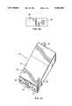
- FIGS. 1A and 1Bare respectively isometric and end views showing the housing of a preferred network adapter in accordance with the present invention
- FIG. 2comprises a functional block diagram of a preferred network adapter in accordance with the present invention
- FIGS. 3A, 3B, and 3Ccomprise block diagrams respectively depicting the configuration of standard parallel ports for the XT, AT, and PS 2 generations of IBM compatible PC's;
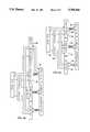
- FIG. 4is a schematic block diagram (partitioned for convenience into FIGS. 4A, 4B, 4C) of the control logic block of FIG. 2;
- FIG. 5is a flow chart depicting the initialization routine executed by the network adapter.
- FIG. 6is a chart functionally depicting the operation of the double quasi nibble transfer operation.
- FIGS. 1A and 1Bshow the external configuration of a preferred embodiment of a network adapter 10 in accordance with the present invention.
- the adapter 10is comprised of a substantially enclosed rectangular housing 12.
- a first connector 14is mounted on one end of the housing 12 for mating connection to a standard PC parallel port D-shell connector.
- First and second captive screws 16 and 18are mounted in the housing 12 for coupling to threaded holes typically provided adjacent a standard PC parallel port connector.
- Thumbwheels 20 and 22are mounted for rotation within recesses in the housing 12 to enable a user to rotate the screws 16 and 18.
- a second connector means 24is mounted on the opposite end of the housing 12.
- the connector means 24is configured to connect to a local area network media, e.g. coaxial cable as is used in standard Ethernet networks.
- the housing 12additionally defines a socket 26 intended to receive a conventional AC adapter jack which supplies DC voltage (e.g. 12 volt D.C. unregulated).
- the purpose of the adapter 10is to enable personal computers, principally IBM and compatible PC's, to be readily connected to local area networks such as Ethernet, Thin Ethernet, Token Ring, Arcnet, etc..
- a network adapter embodiment in accordance with the present inventionis especially configured to work with a specific network.
- a family of different network adaptersbe provided in accordance with the invention, each intended to work with a different type of network.
- the network adapter embodiment 10 depicted in FIGS. 1A and 1Bis intended to work with a Thin Ethernet network using RG-58 coax, compatible with the depicted connector 24.
- the rectangular housing 12is preferably dimensioned to be substantially pocket sized so that it can be conveniently carried by a user.
- the network adapter in accordance with the invention currently being manufactured by the assignee of the present applicationhas a length equal to approximately 5 inches, a width equal to approximately 21/2 inches, and a height equal to approximately 1 inch.
- the adapter 10is intended to readily connect externally to any standard PC parallel port, thus eliminating the difficulty of internally installing prior art circuit board network adapters.
- the external configuration of applicant's network adapter 10, as depicted in FIGS. 1A and 1B,makes it particularly suitable for use with laptop computers and also for PC's in which the available slots, or power, are at a premium.
- FIG. 2comprises a block diagram of the network adapter 10 for functionally connecting a PC 30 via its parallel port 32 to a network media, e.g. coax, 34.
- the network adapter connector 14mates with the connector of the parallel port 32 (to be discussed further in connection with FIG. 3) and the connector 24 mates with the network media 34.
- the network adapter electronicsdepicted in block form in FIG. 2, is carried by a circuit board (not shown) fully contained within the network adapter housing 12 (FIG. 1A).
- the electronicsmay appropriately be considered as being primarily comprised of three functional portions; i.e., a network interface portion 40, an input/output portion 42, and a power supply portion 44.
- the network interface portion 40is primarily comprised of a network interface controller 46, a serial network interface 48, and a transceiver interface 50.
- Devices 46, 48 and 50are readily available as integrated circuit chips and are sold as chip sets by various semiconductor manufacturers. For example only, National Semiconductor markets an Ethernet chip set including a network interface controller DP8390, a serial network interface DP8391 or DP83910 and a coaxial transceiver interface DP8392.
- the network interface portion 40further includes a data packet memory 52 and an address memory 53.
- the integrated operation of the devices 46, 48, 50, 52 and 53is widely discussed in the prior art literature and is characteristic of the aforementioned circuit board type of network adapters which are accommodated in available PC slots.
- the input/output circuit portion 42is primarily comprised of buffers 54, 56 and control logic 58.
- Buffers 54 and 56preferably comprise integrated circuits widely marketed as bus transceivers by various manufacturers, e.g. 74LS devices sold by Texas Instruments.
- the hysteresis characteristics of the buffers 54 and 56improve noise margins by smoothing the level transitions of the output signals supplied by the PC 30 at the parallel port 32. That is, the output signal level transitions delivered by a typical PC at its parallel output port 32 are fairly sloppy or irregular.
- the hysteresis function of the buffers 54and serves to clean up or smooth out the perturbations in those level transitions or signal edges.
- buffer 56is bidirectional and is used to transfer data bytes (eight bits) between the connector 14 and the control logic 58.
- the buffer 54is unidirectional, half (four bits) being used for input signals from connector 14 and the other half (four bits) being used for output signals to connector 14.
- the control logic 58is preferably implemented in a programmable device (e.g. programmable gate array) so that a software device driver executed by the PC 30 will initialize or configure the control logic 58 each time it is booted up. This initialization or configuration procedure will be discussed hereinafter in connection with the flow chart of FIG. 5.
- the control logic 58can be implemented in an application specific integrated circuit (ASIC).
- FIGS. 3A, 3B and 3Crespectively illustrate standard parallel port configurations for the IBM XT, IBM AT, and IBM PS/2 PC's. Note that all three parallel port configurations utilize a standard twenty five pin female connector, previously identified as element 32 in FIG. 2.
- the PC bus 70is internally connected through control logic 72 to a set of control latches 74. Five bit lines 76 connect the unidirectional out control latches 74 to pins on the connector 32. Five additional pins on the connector 32 connect via five status lines 78 to unidirectional in status latches 80 and then to the control logic 72.
- FIG. 3A, 3B and 3Crespectively illustrate standard parallel port configurations for the IBM XT, IBM AT, and IBM PS/2 PC's.
- all three parallel port configurationsutilize a standard twenty five pin female connector, previously identified as element 32 in FIG. 2.
- the PC bus 70is internally connected through control logic 72 to a set of control latches 74.
- Five bit lines 76connect the unidirectional out control latches 74
- a set of eight unidirectional out data latches 82connect the bus 70 through lines 84 to pins on the connector 32.
- the data latches 82are unidirectional out to connector 32 and do not allow for reading data from the connector 32 back into the PC bus 70 via the data lines 84.
- the five status lines 78are used by the network adapter 10 for reading data in to the PC bus 70, four bits at a time. This data transfer mode will hereinafter sometimes be referred to as a double quasi nibble transfer mode.
- the IBM AT parallel port configuration depicted in FIG. 3Bdiffers from the XT configuration in that it includes eight data out-latches 88 and eight data in-latches 90 both connected to the eight data lines 92.
- the AT parallel portwas designed only with data output capability in mind with a readback capability, i.e. via data in-latches 90, for detecting faults.
- the data out-latches 88are not tristatable, i.e. they are always driving out. In operating with the AT configuration of FIG.
- the network adapter 10is able to force the data out-latch 88 to all ones and is able to read data in, eight bits in parallel, via the data in-latch 90, because of its TTL implementation which allows a TTL ground to overcome a TTL high level.
- the AT parallel portinherently allows data bytes to move bidirectionally without any control of the bidirectionality.
- the PC bus 100is connected through a bidirectional data latch 102 to the parallel port connector 32.
- a bit within the control latch 104controls the directionality of the data latch 102 via gate 106.
- a network adapter 10 in accordance with the present inventionsets the bit in the control latch 104 to set the directionality of the data latch 102, that is to either transfer data into or out of the data latch 102 with respect to the connector 32.
- a standard XT parallel port(FIG. 3A) is strictly unidirectional
- standard AT parallel port(FIG. 3B) was designed to be unidirectional but as a consequence of it being able to detect faults, can be used in a bidirectional fashion
- a standard PS/2 parallel port(FIG. 3C) is truly bidirectional and its directionality is controlled by a control bit.
- the letters A-Hhave been applied to various groups of bitlines into and out of the control logic 58. These designating letters have been introduced in FIG. 2 to help key various lines to the detailed control logic schematic of FIG. 4.
- the letter A in FIG. 2has been used to identify four status lines out of control logic 58 which connect via the buffer 54 to the parallel port status lines.
- the status lines Aare used in accordance with the present invention in the double quasi nibble transfer mode to transfer four data bits at a time to the parallel port.
- the letter B in FIG. 2identifies control lines coming into the control logic 58 from the buffer 54, specifically including a register address strobe, a read/write signal, and a register data strobe.
- the letter C in FIG. 2designates the eight bidirectional data lines coupling buffer 56 to control logic 58.
- the letter D in FIG. 2identifies control lines used for control signals from the control logic 58 to the network controller 46.
- the letter Eidentifies eight lines used to transfer data bytes bidirectionally between the control logic 58 and the network controller 46.
- the letter F in FIG. 2identifies address lines for addressing the packet memory 52.
- the letter Gidentifies control lines from control logic 58 to the address memory 54, preferably an electrically erasable read only memory.
- the letter Hidentifies bidirectional data lines between the control logic 58 and the address memory 54.
- FIG. 4depicts a schematic representation of the control logic 58 of FIG. 2 and which relates the assigned letters A-H from FIG. 2 to the various input/output pins of FIG. 4.
- the control logic 58 of FIG. 4is comprised of several readily identifiable functional circuit groups. Note specifically the gate configuration enclosed within dashed box 120 (FIG. 4C), functionally comprising a multiplexer for transferring four bits at a time, during the performance of the double quasi nibble transfer mode, to the line set A.
- Functional circuits 122, 124 (FIG. 4A) and 126 (FIG. 4B)comprise digital debounce circuits which have as their inputs lines, the control line set B shown in FIG. 2. More specifically, debounce circuit 122 has as its input control signal, line B1 comprising the register address strobe.
- Debounce circuits 124 and 126respectively accept as their inputs, the read/write signal and the register data strobe signal.
- the function of the debounce circuits 122, 124, and 126is to remove short term spikes, e.g. less than 500 nanoseconds, from the input control signals. This feature is useful because, together with the hysteresis of the buffers 54, 56, it shapes the signal transitions from the parallel port to remove spurious perturbations. Typically, the falling or leading level or edge transitions of a signal from the parallel port has a relatively long duration of five microseconds or more. This creates the opportunity for a number of perturbations or bounces on the line, some of which are removed by the hysteresis of the buffers 54, 56.
- the debounce circuits 122, 124, 126specifically remove short duration spikes, e.g. less than 500 nanoseconds, by sampling the signals from the buffers at a high clock rate, and then comparing each new sample with N immediately preceding samples. Only if the state of N successive samples are in agreement will the state be accepted for further processing by the control logic 58.
- the functional circuit 128comprises an edge detect and strobe generation circuit for processing the output of digital debounce circuit 126.
- Functional circuit 130comprises a bidirectional buffer for handling eight bit data transfer in each direction.
- the bidirectional buffer 130internally supplies its output to an eight bit latch circuit 132 and also an eight bit register 134.
- the bidirectional buffer 130accepts its input from an eight bit latch 136.
- the bidirectional buffer 130externally interfaces outside with the line set C as indicated in FIGS. 2 and 4.
- a second bidirectional buffer 140is shown in FIG. 4 and this functional circuit interfaces externally with data lines E keyed in FIGS. 2 an 4.
- the bidirectional buffer 140supplies input to the aforementioned eight bit latch 136 (FIG. 4C) as well as eight bit latch 142 (FIG. 4C). Note that the eight bit latch 142 interfaces with line set F keyed in FIGS. 2 and 4.
- the final major functional circuit in FIG. 4comprises control signal decode logic 146 (FIG. 4B) which outputs control signals D (represented in FIG. 4B as D2) to the network controller 46 (FIG. 2).
- the eight bit register 134(FIG. 4A) also supplies an output signal (shown as D1) to the network controller 46.
- Input to the control decode logic 146 (FIG. 4B)is derived from the debounce circuit 124 (FIG. 4A) as well as the edge detect and strobe generation circuit 128 (FIG. 4B) and eight bit register 134 (FIG. 4A).
- control logic 58can be implemented either as an application specific integrated circuit or as a programmable gate array.
- an initialization routine(FIG. 5) must first be executed to download an encoded bitstream which defines the actual logic or schematic depicted in FIG. 4.
- FIG. 5comprises a functional flow chart describing the initialization routine executed each time the adapter 10 is booted up, i.e. reset. More specifically, block 180 in FIG. 5 represents the initial step of the initialization routine, e.g. resetting of adapter 10. Thereafter, the PC configures the gate array (182) to define the control logic schematic as depicted in FIG. 4.
- This stepinvolves downloading the adapter 10 with an encoded bitstream, typically about 12,000 bits long, which serially toggles the gate array.
- the aforementioned register data strobe and address strobe lines, B1 (FIG. 4A) and B3 (FIG. 4B)are used as the clock and data lines for toggling the logic into the gate array. After the gate array has been configured, these lines serve their primary purpose for address and data strobing.
- the PC 30tests the PC parallel port to determine whether it is bidirectional (e.g. AT or PS/2) (FIG. 3B, 3C) or unidirectional (XT) (FIG. 3A).
- Block 184 of FIG. 5indicates that the parallel port is initially assumed to be bidirectional and therefore pointers to the bidirectional read routines as represented by block 186, are installed. Thereafter, as depicted by block 188, a read after write test is performed to successively write 256 different eight bit patterns to the adapter. Each data byte is read immediately after it is written. More specifically, the PC 30 writes a data byte to the adapter control logic 58 which will be latched in both data latches 132 and 134 (FIG. 4A).
- step 192instead of assuming the bidirectionality of the parallel port, unidirectionality is assumed and appropriate pointers are installed to the unidirectional read routines (step 194). Thereafter, the unidirectionability is tested by performing 256 write/read/compare loops in step 196.
- the test performed in 196 utilizing the unidirectional read routines (194)is essentially the same as the bidirectional test performed in step 188. More specifically, all 256 eight bit patterns are written to the control logic 58 via the buffer 130 and into the latches 132 and 134.
- the decision block 198determines whether any mismatches occur in the write/read/compare tests. If none occur, then further operation continues using the unidirectional read routines.
- step 200the adapter will be in one of three states; it will either be configured to function with a bidirectional parallel port, a unidirectional parallel port, or will indicate a failed configuration.
- the adapterAfter the adapter has been configured by the initialization sequence represented in FIG. 5, in its bidirectional mode it can operate similarly to any prior art network adapter.
- existing software device driverswhich are commercially available to function, for example, with Novell or 3-Com network operating systems can be used. That is, a software device driver written for a network operating system such as Novell or 3-Com, is structurally the same as one required to run the network adapter 10 disclosed herein.
- low level differences in the softwaremay be required for reading and writing to particular registers and moving data back and forth between the PC 30 and the adapter 10.
- aforementioned Pocket LAN Adapters marketed by Xircomutilize a set of low level routines to perform these particular functions when porting an existing network operating system driver, as Novell or 3-Com, to a Xircom adapter 10. Very simply, this may involve replacing register access portions of existing software code with calls to these low level routines.
- the coding for these low level routinesis disclosed in applications for copyright registration filed by Xircom on or about Mar. 10, 1990 entitled "Pocket Ethernet Driver” and "Users Manual For The Xircom Driver Development Kit".
- FIG. 6illustrates the operation of the double quasi nibble transfer mode which, as will be recalled, is utilized when the adapter 10 is configured to operate with an XT or unidirectional type parallel port, as depicted in FIG. 3A.
- the upper portion of FIG. 6shows an eight bit data byte 210 to be read from the adapter 10 by the PC 30 across the adapter connector 14 and PC parallel port connector 32.
- the adaptersplits the byte 210 into a quasi low nibble 212 containing original bits 0, 1, 2, 6) and a quasi high nibble 214 (containing bits 3, 4, 5 and 7).
- the quasi nibbles 212 and 214are separately transferred across four of the parallel port status lines (78, FIG. 3A) four bits at a time.
- the high nibble and low nibble portionsare then combined to ultimately recreate the original byte 210. This processing of the two quasi nibbles is depicted in FIG. 6.
- the status lines when read out of the PC parallel port status registercorrespond to bit positions 7, 6, 5, 4, 3 of an eight bit word.
- bit position 6 of the status registeris used as the interrupt line and cannot be used for transferring data. Therefore, the data coming into the four status lines of the PC's parallel port will appear in the status register in bit positions 7, 5, 4, 3.
- the double quasi nibble transfer mode employed in accordance with the invention and depicted in FIG. 6manipulates the two quasi nibbles (high and low) around this limitation to correctly assemble a data byte. That is, note in FIG. 6 that the bits 7, 5, 4, 3 of high nibble 214 are read on to the four status lines and are stored as a partial byte in PC processor register AH.
- Bit position 6, 2, 1, 0 of the status registerare masked to 0.
- the low nibble 212which consists of bits 6, 2, 1, 0 are applied to the same four status lines but must be operated upon to move these bits into the right positions for combining with the stored partial byte in aforementioned register AH.
- Note in FIG. 6that the low nibble bits 6, 2, 1, 0 are respectively brought in to the status register in positions 7, 5, 4, 3 (216) and then arithmetically shifted right three times to produce the eight bit group 218. Then, by masking to 0 positions 7, 5, 4, 3, the bits 6, 2, 1, 0 are moved into their proper position and can be stored as a partial byte in processor register AL.
- An adapter in accordance with the inventionis characterized by a substantially enclosed rectangular housing having an external connector at one end for connection to a parallel port and a network media connector at an opposite end.
- the parallel portis tested during an initialization procedure to determine whether it is capable of operating in a bidirectional data transfer mode or unidirectional data transfer mode. This characteristic of the parallel port determines how the adapter transfers data bytes to the PC via the parallel port. If the parallel port is only capable of operating in a unidirectional mode, then the adapter operates in a double quasi nibble transfer mode as depicted in FIG. 6 to sequentially transfer partial bytes to the PC.
Landscapes
- Engineering & Computer Science (AREA)
- Theoretical Computer Science (AREA)
- Physics & Mathematics (AREA)
- General Engineering & Computer Science (AREA)
- General Physics & Mathematics (AREA)
- Computer And Data Communications (AREA)
Abstract
Description
Claims (30)
Priority Applications (2)
| Application Number | Priority Date | Filing Date | Title |
|---|---|---|---|
| US08/117,990US5299314A (en) | 1990-03-22 | 1993-09-08 | Network adapter using status inlines and data lines for bi-directionally transferring data between lan and standard p.c. parallel port |
| US08/623,457USRE36904E (en) | 1990-03-22 | 1996-03-28 | Network adapter using status inlines and data lines for bi-directionally transferring data between LAN and standard P.C. parallel port |
Applications Claiming Priority (2)
| Application Number | Priority Date | Filing Date | Title |
|---|---|---|---|
| US49734190A | 1990-03-22 | 1990-03-22 | |
| US08/117,990US5299314A (en) | 1990-03-22 | 1993-09-08 | Network adapter using status inlines and data lines for bi-directionally transferring data between lan and standard p.c. parallel port |
Related Parent Applications (1)
| Application Number | Title | Priority Date | Filing Date |
|---|---|---|---|
| US49734190AContinuation | 1990-03-22 | 1990-03-22 |
Publications (1)
| Publication Number | Publication Date |
|---|---|
| US5299314Atrue US5299314A (en) | 1994-03-29 |
Family
ID=23976469
Family Applications (2)
| Application Number | Title | Priority Date | Filing Date |
|---|---|---|---|
| US08/117,990CeasedUS5299314A (en) | 1990-03-22 | 1993-09-08 | Network adapter using status inlines and data lines for bi-directionally transferring data between lan and standard p.c. parallel port |
| US08/623,457Expired - LifetimeUSRE36904E (en) | 1990-03-22 | 1996-03-28 | Network adapter using status inlines and data lines for bi-directionally transferring data between LAN and standard P.C. parallel port |
Family Applications After (1)
| Application Number | Title | Priority Date | Filing Date |
|---|---|---|---|
| US08/623,457Expired - LifetimeUSRE36904E (en) | 1990-03-22 | 1996-03-28 | Network adapter using status inlines and data lines for bi-directionally transferring data between LAN and standard P.C. parallel port |
Country Status (1)
| Country | Link |
|---|---|
| US (2) | US5299314A (en) |
Cited By (44)
| Publication number | Priority date | Publication date | Assignee | Title |
|---|---|---|---|---|
| WO1994018619A1 (en)* | 1993-02-10 | 1994-08-18 | Oakleigh Systems, Inc. | Extended enhanced parallel port |
| US5408614A (en)* | 1993-12-17 | 1995-04-18 | Xircom, Inc. | Modem adapter for use with standard PC parallel port |
| US5423005A (en)* | 1990-10-11 | 1995-06-06 | Telemecanique | Programmable automatic controller having a configuration circuit cooperating with a monitor logic to selectively transmit a different return output frame |
| US5490283A (en)* | 1992-09-16 | 1996-02-06 | Ultima Electronics Corporation | Adapter with FIFO and buffers for interfacing a handheld scanner to the parallel printer port of a portable computer |
| WO1996006398A1 (en)* | 1994-08-19 | 1996-02-29 | Visioneer, Inc. | Method and apparatus for high-speed communication between computer and peripherals |
| US5504929A (en)* | 1993-11-17 | 1996-04-02 | Adobe Systems Incorporated | Method and apparatus for encoding byte sequence for self-clocked high speed data transfer from a parallel port |
| US5507003A (en)* | 1991-08-27 | 1996-04-09 | Compaq Computer Corp | Parallel interface protocol for bidirectional communications between computer and printer using status lines for transmitting data during a reverse channel operation |
| US5513325A (en)* | 1992-12-23 | 1996-04-30 | Unisys Corporation | Technique for coupling CTOS units to non-CTOS host |
| US5555374A (en)* | 1994-08-26 | 1996-09-10 | Systech Computer Corporation | System and method for coupling a plurality of peripheral devices to a host computer through a host computer parallel port |
| US5555440A (en)* | 1992-03-10 | 1996-09-10 | Siemens Nixdorf Informationssysteme Aktiengesellschaft | Parallel interface for connecting data processing devices to one another over bidirectional control lines |
| US5600793A (en)* | 1994-12-20 | 1997-02-04 | International Business Machines Corporation | Method and system of bi-directional parallel port data transfer between data processing systems |
| US5636348A (en)* | 1992-05-15 | 1997-06-03 | Zenith Data Systems Corporation | Control system for a multiple mode standard parallel port for a personal computer |
| US5644593A (en)* | 1994-09-02 | 1997-07-01 | Microcom Systems, Inc. | High performance communications interface |
| US5659684A (en)* | 1995-02-03 | 1997-08-19 | Isdn Systems Corporation | Methods and apparatus for interconnecting personal computers (PCs) and local area networks (LANs) using packet protocols transmitted over a digital data service (DDS) |
| US5696993A (en)* | 1993-12-03 | 1997-12-09 | Intel Corporation | Apparatus for decoding and providing the decoded addresses to industry standard PCMCIA card through the data lines of the parallel port |
| US5724066A (en)* | 1994-03-10 | 1998-03-03 | Boehringer Mannheim Corporation | Method and apparatus for automatic control of instruments through video |
| US5732199A (en)* | 1996-09-25 | 1998-03-24 | Behavior Tech Computer Corporation | Control method and device of scanner with built-in plug-and-play printer port |
| US5761428A (en)* | 1996-07-05 | 1998-06-02 | Ncr Corporation | Method and aparatus for providing agent capability independent from a network node |
| US5812879A (en)* | 1993-04-19 | 1998-09-22 | Moro; Ricardo J. | External multiple peripheral interface to computer serial port using individually configured parallel port terminals |
| US5815722A (en)* | 1992-11-18 | 1998-09-29 | Canon Information Systems, Inc. | In an interactive network board, a method and apparatus for remotely downloading and executing files in a memory |
| US5828905A (en)* | 1995-11-13 | 1998-10-27 | Mitsubishi Chemical America, Inc. | Adapter and method of connecting devices associated with at least three different protocols |
| US5896512A (en)* | 1996-09-11 | 1999-04-20 | Lucent Technologies Inc. | Modified network interface unit with terminal device access |
| US6014716A (en)* | 1996-07-01 | 2000-01-11 | Brother Kogyo Kabushiki Kaisha | System for recognizing bidirectional communication over parrallel data lines by further sending data transmission request and notification indicating reverse direction transmission is possible to second device |
| US6061742A (en)* | 1997-10-10 | 2000-05-09 | Nortel Networks Corporation | Computer network adaptor |
| US6141706A (en)* | 1993-12-17 | 2000-10-31 | Xircom, Inc. | Communication method for redirecting information to another port |
| USRE37118E1 (en)* | 1992-11-13 | 2001-03-27 | Video Associates Labs, Inc. | System for transmitting and receiving combination of compressed digital information and embedded strobe bit between computer and external device through parallel printer port of computer |
| WO2001031426A1 (en)* | 1999-10-19 | 2001-05-03 | Viator Networks, Inc. | Adapter for connecting a computer system to a computer network |
| US20010036199A1 (en)* | 2000-03-30 | 2001-11-01 | Terry John B. | Architecture and method for automatic distributed gain control for modem communications over passive multipoint networks |
| US6324598B1 (en)* | 1999-01-11 | 2001-11-27 | Oak Technology | Software enlarged tag register and method thereof for noting the completion of a DMA transfer within a chain of DMA transfers |
| US6389029B1 (en) | 1998-11-10 | 2002-05-14 | Nortel Networks Limited | Local area network incorporating universal serial bus protocol |
| US20020078128A1 (en)* | 2000-12-14 | 2002-06-20 | Peshkin Joel D. | Intelligent network interface port for visiting computers |
| US20020101824A1 (en)* | 2000-03-28 | 2002-08-01 | Ziedman Robert M. | System and method for connecting a logic circuit simulation to a network |
| US20030167347A1 (en)* | 2002-02-11 | 2003-09-04 | Combs James Lee | Home network printer adapter |
| US20030198242A1 (en)* | 2000-03-28 | 2003-10-23 | Zeidman Robert M. | Method for connecting a hardware emulator to a network |
| US6651107B1 (en) | 1999-09-21 | 2003-11-18 | Intel Corporation | Reduced hardware network adapter and communication |
| US6658459B1 (en)* | 1998-02-27 | 2003-12-02 | Adaptec, Inc. | System for sharing peripheral devices over a network and method for implementing the same |
| US20040117509A1 (en)* | 1997-10-14 | 2004-06-17 | Alacritech, Inc. | Protocol processing stack for use with intelligent network interface device |
| US20050021996A1 (en)* | 2003-07-22 | 2005-01-27 | Howard Robert James | Method and apparatus for preventing un-authorized attachment of computer peripherals |
| US6967960B1 (en)* | 2000-03-31 | 2005-11-22 | Intel Corporation | Method and apparatus for emulating a local data port |
| US20070061127A1 (en)* | 2000-03-28 | 2007-03-15 | Zeidman Robert M | Apparatus and method for connecting hardware to a circuit simulation |
| US7380044B1 (en)* | 2006-04-17 | 2008-05-27 | Francesco Liburdi | IEEE 1394 to coaxial cable adapter |
| US20100132046A1 (en)* | 2008-11-25 | 2010-05-27 | Thales | Electronic Circuit for Securing Data Interchanges Between a Computer Station and a Network |
| US10320484B2 (en)* | 2015-05-11 | 2019-06-11 | Neptune Subsea Ip Limited | Optical networking with support for unidirectional optical links |
| US10986165B2 (en) | 2004-01-13 | 2021-04-20 | May Patents Ltd. | Information device |
Families Citing this family (1)
| Publication number | Priority date | Publication date | Assignee | Title |
|---|---|---|---|---|
| CN110956007A (en)* | 2019-12-06 | 2020-04-03 | 国微集团(深圳)有限公司 | Method and system for checking simulation signal of digital product |
Citations (19)
| Publication number | Priority date | Publication date | Assignee | Title |
|---|---|---|---|---|
| US4417320A (en)* | 1981-05-11 | 1983-11-22 | Interface Systems, Inc. | Interface for data communication systems using serial biphase data transmissions |
| US4493021A (en)* | 1981-04-03 | 1985-01-08 | The United States Of America As Represented By The Administrator Of The National Aeronautics And Space Administration | Multicomputer communication system |
| US4635222A (en)* | 1982-08-20 | 1987-01-06 | Pioneer Electronic Corporation | Interface device for converting a computer printer port into an input/output port |
| US4672570A (en)* | 1986-09-05 | 1987-06-09 | The United States Of America As Represented By The Secretary Of The Air Force | Network interface module and method |
| US4703450A (en)* | 1982-08-20 | 1987-10-27 | Pioneer Electronic Corporation | Interface device |
| US4777595A (en)* | 1982-05-07 | 1988-10-11 | Digital Equipment Corporation | Apparatus for transferring blocks of information from one node to a second node in a computer network |
| US4812847A (en)* | 1987-10-02 | 1989-03-14 | Stewart John L | Parallel port pass-through digital to analog converter |
| US4851997A (en)* | 1986-02-26 | 1989-07-25 | Mitsubishi Denki Kabushiki Kaisha | Local area network control apparatus |
| US4868848A (en)* | 1987-12-21 | 1989-09-19 | Gte North Incorporated | Computer operated system for dialing telephone numbers |
| US4914688A (en)* | 1987-09-01 | 1990-04-03 | Murata Mfg. Co., Ltd. | Modem system |
| US4958342A (en)* | 1987-03-11 | 1990-09-18 | Aristacom International, Inc. | Adaptive digital network interface |
| US4969083A (en)* | 1988-04-04 | 1990-11-06 | Petron Controls Corporation | Network programmable logic controller system |
| GB2234093A (en)* | 1989-06-21 | 1991-01-23 | Stratum Technology Limited | Data store connection |
| US4991085A (en)* | 1988-04-13 | 1991-02-05 | Chips And Technologies, Inc. | Personal computer bus interface chip with multi-function address relocation pins |
| US5092791A (en)* | 1989-11-28 | 1992-03-03 | L-Com, Inc. | Bulkhead feedthrough adaptor for IEEEE-488 cables |
| US5113497A (en)* | 1988-03-30 | 1992-05-12 | Kabushiki Kaisha Toshiba | I/o control system for a plurality of peripheral devices |
| US5119020A (en)* | 1989-11-06 | 1992-06-02 | Woven Electronics Corporation | Electrical cable assembly for a signal measuring instrument and method |
| US5133055A (en)* | 1990-01-16 | 1992-07-21 | Physio Systems, Inc. | Signal processor for personal computers |
| US5187645A (en)* | 1991-06-07 | 1993-02-16 | Ergo Computing, Inc. | Portable computer with docking connector for peripheral devices |
- 1993
- 1993-09-08USUS08/117,990patent/US5299314A/ennot_activeCeased
- 1996
- 1996-03-28USUS08/623,457patent/USRE36904E/ennot_activeExpired - Lifetime
Patent Citations (19)
| Publication number | Priority date | Publication date | Assignee | Title |
|---|---|---|---|---|
| US4493021A (en)* | 1981-04-03 | 1985-01-08 | The United States Of America As Represented By The Administrator Of The National Aeronautics And Space Administration | Multicomputer communication system |
| US4417320A (en)* | 1981-05-11 | 1983-11-22 | Interface Systems, Inc. | Interface for data communication systems using serial biphase data transmissions |
| US4777595A (en)* | 1982-05-07 | 1988-10-11 | Digital Equipment Corporation | Apparatus for transferring blocks of information from one node to a second node in a computer network |
| US4635222A (en)* | 1982-08-20 | 1987-01-06 | Pioneer Electronic Corporation | Interface device for converting a computer printer port into an input/output port |
| US4703450A (en)* | 1982-08-20 | 1987-10-27 | Pioneer Electronic Corporation | Interface device |
| US4851997A (en)* | 1986-02-26 | 1989-07-25 | Mitsubishi Denki Kabushiki Kaisha | Local area network control apparatus |
| US4672570A (en)* | 1986-09-05 | 1987-06-09 | The United States Of America As Represented By The Secretary Of The Air Force | Network interface module and method |
| US4958342A (en)* | 1987-03-11 | 1990-09-18 | Aristacom International, Inc. | Adaptive digital network interface |
| US4914688A (en)* | 1987-09-01 | 1990-04-03 | Murata Mfg. Co., Ltd. | Modem system |
| US4812847A (en)* | 1987-10-02 | 1989-03-14 | Stewart John L | Parallel port pass-through digital to analog converter |
| US4868848A (en)* | 1987-12-21 | 1989-09-19 | Gte North Incorporated | Computer operated system for dialing telephone numbers |
| US5113497A (en)* | 1988-03-30 | 1992-05-12 | Kabushiki Kaisha Toshiba | I/o control system for a plurality of peripheral devices |
| US4969083A (en)* | 1988-04-04 | 1990-11-06 | Petron Controls Corporation | Network programmable logic controller system |
| US4991085A (en)* | 1988-04-13 | 1991-02-05 | Chips And Technologies, Inc. | Personal computer bus interface chip with multi-function address relocation pins |
| GB2234093A (en)* | 1989-06-21 | 1991-01-23 | Stratum Technology Limited | Data store connection |
| US5119020A (en)* | 1989-11-06 | 1992-06-02 | Woven Electronics Corporation | Electrical cable assembly for a signal measuring instrument and method |
| US5092791A (en)* | 1989-11-28 | 1992-03-03 | L-Com, Inc. | Bulkhead feedthrough adaptor for IEEEE-488 cables |
| US5133055A (en)* | 1990-01-16 | 1992-07-21 | Physio Systems, Inc. | Signal processor for personal computers |
| US5187645A (en)* | 1991-06-07 | 1993-02-16 | Ergo Computing, Inc. | Portable computer with docking connector for peripheral devices |
Cited By (65)
| Publication number | Priority date | Publication date | Assignee | Title |
|---|---|---|---|---|
| US5423005A (en)* | 1990-10-11 | 1995-06-06 | Telemecanique | Programmable automatic controller having a configuration circuit cooperating with a monitor logic to selectively transmit a different return output frame |
| US5507003A (en)* | 1991-08-27 | 1996-04-09 | Compaq Computer Corp | Parallel interface protocol for bidirectional communications between computer and printer using status lines for transmitting data during a reverse channel operation |
| US5555440A (en)* | 1992-03-10 | 1996-09-10 | Siemens Nixdorf Informationssysteme Aktiengesellschaft | Parallel interface for connecting data processing devices to one another over bidirectional control lines |
| US5636348A (en)* | 1992-05-15 | 1997-06-03 | Zenith Data Systems Corporation | Control system for a multiple mode standard parallel port for a personal computer |
| US5490283A (en)* | 1992-09-16 | 1996-02-06 | Ultima Electronics Corporation | Adapter with FIFO and buffers for interfacing a handheld scanner to the parallel printer port of a portable computer |
| USRE37118E1 (en)* | 1992-11-13 | 2001-03-27 | Video Associates Labs, Inc. | System for transmitting and receiving combination of compressed digital information and embedded strobe bit between computer and external device through parallel printer port of computer |
| US5815722A (en)* | 1992-11-18 | 1998-09-29 | Canon Information Systems, Inc. | In an interactive network board, a method and apparatus for remotely downloading and executing files in a memory |
| US5754769A (en)* | 1992-12-23 | 1998-05-19 | Unisys Corp. | Coupling between non-CTOS host and CTOS network |
| US5594870A (en)* | 1992-12-23 | 1997-01-14 | Unisys Corporation | Adapter between non-CTOS host and CTOS network |
| US5513325A (en)* | 1992-12-23 | 1996-04-30 | Unisys Corporation | Technique for coupling CTOS units to non-CTOS host |
| US5457785A (en)* | 1993-02-10 | 1995-10-10 | Elonex Technologies, Inc. | CPU-independent and device-driver transparent system for translating a computer's internal bus signals onto an intermediate bus and further translating onto an expansion bus |
| WO1994018619A1 (en)* | 1993-02-10 | 1994-08-18 | Oakleigh Systems, Inc. | Extended enhanced parallel port |
| US5812879A (en)* | 1993-04-19 | 1998-09-22 | Moro; Ricardo J. | External multiple peripheral interface to computer serial port using individually configured parallel port terminals |
| US5504929A (en)* | 1993-11-17 | 1996-04-02 | Adobe Systems Incorporated | Method and apparatus for encoding byte sequence for self-clocked high speed data transfer from a parallel port |
| US5696993A (en)* | 1993-12-03 | 1997-12-09 | Intel Corporation | Apparatus for decoding and providing the decoded addresses to industry standard PCMCIA card through the data lines of the parallel port |
| US5408614A (en)* | 1993-12-17 | 1995-04-18 | Xircom, Inc. | Modem adapter for use with standard PC parallel port |
| US6141706A (en)* | 1993-12-17 | 2000-10-31 | Xircom, Inc. | Communication method for redirecting information to another port |
| US6049836A (en)* | 1994-03-10 | 2000-04-11 | Roche Diagnostics Corporation | Method and apparatus for automatic control of instruments through video signals |
| US5724066A (en)* | 1994-03-10 | 1998-03-03 | Boehringer Mannheim Corporation | Method and apparatus for automatic control of instruments through video |
| WO1996006398A1 (en)* | 1994-08-19 | 1996-02-29 | Visioneer, Inc. | Method and apparatus for high-speed communication between computer and peripherals |
| US5555374A (en)* | 1994-08-26 | 1996-09-10 | Systech Computer Corporation | System and method for coupling a plurality of peripheral devices to a host computer through a host computer parallel port |
| US5644593A (en)* | 1994-09-02 | 1997-07-01 | Microcom Systems, Inc. | High performance communications interface |
| US5600793A (en)* | 1994-12-20 | 1997-02-04 | International Business Machines Corporation | Method and system of bi-directional parallel port data transfer between data processing systems |
| US5659684A (en)* | 1995-02-03 | 1997-08-19 | Isdn Systems Corporation | Methods and apparatus for interconnecting personal computers (PCs) and local area networks (LANs) using packet protocols transmitted over a digital data service (DDS) |
| US5828905A (en)* | 1995-11-13 | 1998-10-27 | Mitsubishi Chemical America, Inc. | Adapter and method of connecting devices associated with at least three different protocols |
| US6014716A (en)* | 1996-07-01 | 2000-01-11 | Brother Kogyo Kabushiki Kaisha | System for recognizing bidirectional communication over parrallel data lines by further sending data transmission request and notification indicating reverse direction transmission is possible to second device |
| US5761428A (en)* | 1996-07-05 | 1998-06-02 | Ncr Corporation | Method and aparatus for providing agent capability independent from a network node |
| US5896512A (en)* | 1996-09-11 | 1999-04-20 | Lucent Technologies Inc. | Modified network interface unit with terminal device access |
| US5732199A (en)* | 1996-09-25 | 1998-03-24 | Behavior Tech Computer Corporation | Control method and device of scanner with built-in plug-and-play printer port |
| US6061742A (en)* | 1997-10-10 | 2000-05-09 | Nortel Networks Corporation | Computer network adaptor |
| US6502129B1 (en) | 1997-10-10 | 2002-12-31 | Nortel Networks Limited | Computer network adaptor |
| US6941386B2 (en)* | 1997-10-14 | 2005-09-06 | Alacritech, Inc. | Protocol processing stack for use with intelligent network interface device |
| US20040117509A1 (en)* | 1997-10-14 | 2004-06-17 | Alacritech, Inc. | Protocol processing stack for use with intelligent network interface device |
| US6658459B1 (en)* | 1998-02-27 | 2003-12-02 | Adaptec, Inc. | System for sharing peripheral devices over a network and method for implementing the same |
| US6389029B1 (en) | 1998-11-10 | 2002-05-14 | Nortel Networks Limited | Local area network incorporating universal serial bus protocol |
| US6324598B1 (en)* | 1999-01-11 | 2001-11-27 | Oak Technology | Software enlarged tag register and method thereof for noting the completion of a DMA transfer within a chain of DMA transfers |
| US20060184698A1 (en)* | 1999-09-21 | 2006-08-17 | Xircom, Inc. | Reduced hardware network adapter and communication method |
| US20040139220A1 (en)* | 1999-09-21 | 2004-07-15 | Intel Corporation | Reduced hardware network adapter and communication method |
| US7080162B2 (en) | 1999-09-21 | 2006-07-18 | Intel Corporation | Reduced hardware network adapter and communication method |
| US6651107B1 (en) | 1999-09-21 | 2003-11-18 | Intel Corporation | Reduced hardware network adapter and communication |
| EP1232428A4 (en)* | 1999-10-19 | 2003-07-16 | Viator Networks Inc | Adapter for connecting a computer system to a computer network |
| WO2001031426A1 (en)* | 1999-10-19 | 2001-05-03 | Viator Networks, Inc. | Adapter for connecting a computer system to a computer network |
| US20020101824A1 (en)* | 2000-03-28 | 2002-08-01 | Ziedman Robert M. | System and method for connecting a logic circuit simulation to a network |
| US8195442B2 (en) | 2000-03-28 | 2012-06-05 | Ionipas Transfer Company, Llc | Use of hardware peripheral devices with software simulations |
| US20070064694A1 (en)* | 2000-03-28 | 2007-03-22 | Ziedman Robert M | System and method for connecting a logic circuit simulation to a network |
| US7835897B2 (en) | 2000-03-28 | 2010-11-16 | Robert Marc Zeidman | Apparatus and method for connecting hardware to a circuit simulation |
| US7050962B2 (en)* | 2000-03-28 | 2006-05-23 | Zeidman Robert M | Method for connecting a hardware emulator to a network |
| US20030198242A1 (en)* | 2000-03-28 | 2003-10-23 | Zeidman Robert M. | Method for connecting a hardware emulator to a network |
| US20070061127A1 (en)* | 2000-03-28 | 2007-03-15 | Zeidman Robert M | Apparatus and method for connecting hardware to a circuit simulation |
| US8160863B2 (en)* | 2000-03-28 | 2012-04-17 | Ionipas Transfer Company, Llc | System and method for connecting a logic circuit simulation to a network |
| US8380481B2 (en) | 2000-03-28 | 2013-02-19 | Ionipas Transfer Company, Llc | Conveying data from a hardware device to a circuit simulation |
| US20110125479A1 (en)* | 2000-03-28 | 2011-05-26 | Robert Marc Zeidman | Use of hardware peripheral devices with software simulations |
| US20010036199A1 (en)* | 2000-03-30 | 2001-11-01 | Terry John B. | Architecture and method for automatic distributed gain control for modem communications over passive multipoint networks |
| US6967960B1 (en)* | 2000-03-31 | 2005-11-22 | Intel Corporation | Method and apparatus for emulating a local data port |
| US7089334B2 (en)* | 2000-12-14 | 2006-08-08 | Mindspeed Technologies, Inc. | Intelligent network interface port for visiting computers |
| US20020078128A1 (en)* | 2000-12-14 | 2002-06-20 | Peshkin Joel D. | Intelligent network interface port for visiting computers |
| US20030167347A1 (en)* | 2002-02-11 | 2003-09-04 | Combs James Lee | Home network printer adapter |
| US20050021996A1 (en)* | 2003-07-22 | 2005-01-27 | Howard Robert James | Method and apparatus for preventing un-authorized attachment of computer peripherals |
| US7409563B2 (en)* | 2003-07-22 | 2008-08-05 | Lockheed Martin Corporation | Method and apparatus for preventing un-authorized attachment of computer peripherals |
| US10986165B2 (en) | 2004-01-13 | 2021-04-20 | May Patents Ltd. | Information device |
| US7380044B1 (en)* | 2006-04-17 | 2008-05-27 | Francesco Liburdi | IEEE 1394 to coaxial cable adapter |
| US20100132046A1 (en)* | 2008-11-25 | 2010-05-27 | Thales | Electronic Circuit for Securing Data Interchanges Between a Computer Station and a Network |
| US8577035B2 (en)* | 2008-11-25 | 2013-11-05 | Thales | Electronic circuit for securing data interchanges between a computer station and a network |
| US10320484B2 (en)* | 2015-05-11 | 2019-06-11 | Neptune Subsea Ip Limited | Optical networking with support for unidirectional optical links |
| US10404374B1 (en)* | 2015-05-11 | 2019-09-03 | Neptune Subsea Ip Limited | Optical networking with support for unidirectional optical links |
Also Published As
| Publication number | Publication date |
|---|---|
| USRE36904E (en) | 2000-10-03 |
Similar Documents
| Publication | Publication Date | Title |
|---|---|---|
| US5299314A (en) | Network adapter using status inlines and data lines for bi-directionally transferring data between lan and standard p.c. parallel port | |
| US7231560B2 (en) | Apparatus and method for testing motherboard having PCI express devices | |
| US7498801B2 (en) | Apparatus, method, and computer program product for monitoring and controlling a microcomputer using a single existing pin | |
| US6349331B1 (en) | Multiple channel communication system with shared autonegotiation controller | |
| US5440755A (en) | Computer system with a processor-direct universal bus connector and interchangeable bus translator | |
| US5321819A (en) | Interface for coupling a host device having a network interface to a computer network having a predetermined communications medium and a predetermined communications physical layer | |
| EP0798894B1 (en) | Management communication bus for networking devices | |
| CA2189782C (en) | System and method for expansion of a computer | |
| US20100122003A1 (en) | Ring-based high speed bus interface | |
| US4417320A (en) | Interface for data communication systems using serial biphase data transmissions | |
| CN104838636A (en) | Ethernet over USB interface with full-duplex differential pair | |
| GB2288954A (en) | Programmable serial communications | |
| JP3759234B2 (en) | Communication interface using UART software simulation and conflict avoidance | |
| WO2004023268A9 (en) | Method and apparatus for double data rate serial ata phy interface | |
| US20200409706A1 (en) | Apparatuses and methods involving selective disablement of side effects caused by accessing register sets | |
| US5557741A (en) | Test apparatus and method for a computer parallel port | |
| US20050097403A1 (en) | USB interface and testing method thereof | |
| US20020101824A1 (en) | System and method for connecting a logic circuit simulation to a network | |
| US7633877B2 (en) | Method and apparatus for meeting compliance for debugging and testing a multi-speed, point-to-point link | |
| US20060248391A1 (en) | State machine-based command line debugger | |
| US6493647B1 (en) | Method and apparatus for exercising external memory with a memory built-in self-test | |
| US7050962B2 (en) | Method for connecting a hardware emulator to a network | |
| TWI727581B (en) | Data transmission system | |
| CN118041451A (en) | Pluggable optical module and debugging method thereof | |
| US5754769A (en) | Coupling between non-CTOS host and CTOS network |
Legal Events
| Date | Code | Title | Description |
|---|---|---|---|
| STCF | Information on status: patent grant | Free format text:PATENTED CASE | |
| RF | Reissue application filed | Effective date:19960328 | |
| FEPP | Fee payment procedure | Free format text:PAT HLDR NO LONGER CLAIMS SMALL ENT STAT AS INDIV INVENTOR (ORIGINAL EVENT CODE: LSM1); ENTITY STATUS OF PATENT OWNER: LARGE ENTITY Free format text:PAYOR NUMBER ASSIGNED (ORIGINAL EVENT CODE: ASPN); ENTITY STATUS OF PATENT OWNER: LARGE ENTITY | |
| REFU | Refund | Free format text:REFUND - PAYMENT OF MAINTENANCE FEE, 4TH YR, SMALL ENTITY (ORIGINAL EVENT CODE: R283); ENTITY STATUS OF PATENT OWNER: LARGE ENTITY | |
| AS | Assignment | Owner name:NATIONSBANK OF TEXAS, N.A., TEXAS Free format text:SECURITY AGREEMENT;ASSIGNOR:XIRCOM, INC.;REEL/FRAME:008321/0875 Effective date:19961230 | |
| FPAY | Fee payment | Year of fee payment:4 | |
| AS | Assignment | Owner name:XIRCOM, INC., CALIFORNIA Free format text:ASSIGNMENT OF ASSIGNORS INTEREST;ASSIGNOR:GATES, DIRK I.;REEL/FRAME:009360/0501 Effective date:19980724 | |
| AS | Assignment | Owner name:XIRCOM, INC., CALIFORNIA Free format text:FULL RELEASE OF LIEN;ASSIGNOR:BANK OF AMERICA, N.A., F/K/A NATIONSBANK, N.A.;REEL/FRAME:010639/0262 Effective date:20000127 | |
| AS | Assignment | Owner name:XIRCOM, INC., CALIFORNIA Free format text:SECURITY RELEASE;ASSIGNOR:CIT GROUP/CREDIT FINANCE;REEL/FRAME:011506/0741 Effective date:20010111 | |
| AS | Assignment | Owner name:INTEL CORPORATION, CALIFORNIA Free format text:ASSIGNMENT OF ASSIGNORS INTEREST;ASSIGNOR:XIRCOM, INC.;REEL/FRAME:013193/0088 Effective date:20020725 | |
| FEPP | Fee payment procedure | Free format text:PAYOR NUMBER ASSIGNED (ORIGINAL EVENT CODE: ASPN); ENTITY STATUS OF PATENT OWNER: LARGE ENTITY Free format text:PAYER NUMBER DE-ASSIGNED (ORIGINAL EVENT CODE: RMPN); ENTITY STATUS OF PATENT OWNER: LARGE ENTITY |