US5298685A - Interconnection method and structure for organic circuit boards - Google Patents
Interconnection method and structure for organic circuit boardsDownload PDFInfo
- Publication number
- US5298685A US5298685AUS07/913,086US91308692AUS5298685AUS 5298685 AUS5298685 AUS 5298685AUS 91308692 AUS91308692 AUS 91308692AUS 5298685 AUS5298685 AUS 5298685A
- Authority
- US
- United States
- Prior art keywords
- subcomposites
- electrical contact
- contact pads
- dendrites
- circuit board
- Prior art date
- Legal status (The legal status is an assumption and is not a legal conclusion. Google has not performed a legal analysis and makes no representation as to the accuracy of the status listed.)
- Expired - Fee Related
Links
- 238000000034methodMethods0.000titledescription22
- 210000001787dendriteAnatomy0.000claimsabstractdescription29
- KDLHZDBZIXYQEI-UHFFFAOYSA-NPalladiumChemical compound[Pd]KDLHZDBZIXYQEI-UHFFFAOYSA-N0.000claimsdescription32
- 239000000463materialSubstances0.000claimsdescription17
- 229910052763palladiumInorganic materials0.000claimsdescription16
- 239000002131composite materialSubstances0.000claimsdescription11
- RYGMFSIKBFXOCR-UHFFFAOYSA-NCopperChemical compound[Cu]RYGMFSIKBFXOCR-UHFFFAOYSA-N0.000claimsdescription8
- 229910052802copperInorganic materials0.000claimsdescription8
- 239000010949copperSubstances0.000claimsdescription8
- ATJFFYVFTNAWJD-UHFFFAOYSA-NTinChemical compound[Sn]ATJFFYVFTNAWJD-UHFFFAOYSA-N0.000claimsdescription5
- PCHJSUWPFVWCPO-UHFFFAOYSA-NgoldChemical compound[Au]PCHJSUWPFVWCPO-UHFFFAOYSA-N0.000claimsdescription5
- 229910052737goldInorganic materials0.000claimsdescription5
- 239000010931goldSubstances0.000claimsdescription5
- 238000010438heat treatmentMethods0.000claimsdescription5
- 229910052751metalInorganic materials0.000claimsdescription4
- 239000002184metalSubstances0.000claimsdescription4
- 238000002844meltingMethods0.000claimsdescription2
- 230000008018meltingEffects0.000claimsdescription2
- 239000010410layerSubstances0.000description25
- PXHVJJICTQNCMI-UHFFFAOYSA-NNickelChemical compound[Ni]PXHVJJICTQNCMI-UHFFFAOYSA-N0.000description12
- 239000000758substrateSubstances0.000description9
- 238000004806packaging method and processMethods0.000description7
- -1polypropylenePolymers0.000description7
- 229910052759nickelInorganic materials0.000description6
- 239000003989dielectric materialSubstances0.000description5
- 230000008569processEffects0.000description5
- 239000000203mixtureSubstances0.000description4
- ISWSIDIOOBJBQZ-UHFFFAOYSA-Nphenol groupChemical groupC1(=CC=CC=C1)OISWSIDIOOBJBQZ-UHFFFAOYSA-N0.000description4
- 229920000642polymerPolymers0.000description4
- 238000004891communicationMethods0.000description3
- 238000005516engineering processMethods0.000description3
- 229920002120photoresistant polymerPolymers0.000description3
- 238000007747platingMethods0.000description3
- 229920001343polytetrafluoroethylenePolymers0.000description3
- 239000004810polytetrafluoroethyleneSubstances0.000description3
- 229920001169thermoplasticPolymers0.000description3
- 229920001187thermosetting polymerPolymers0.000description3
- 239000004416thermosoftening plasticSubstances0.000description3
- 229910001374InvarInorganic materials0.000description2
- 239000000919ceramicSubstances0.000description2
- UUAGAQFQZIEFAH-UHFFFAOYSA-NchlorotrifluoroethyleneChemical groupFC(F)=C(F)ClUUAGAQFQZIEFAH-UHFFFAOYSA-N0.000description2
- 239000004020conductorSubstances0.000description2
- 239000004744fabricSubstances0.000description2
- 239000000945fillerSubstances0.000description2
- NBVXSUQYWXRMNV-UHFFFAOYSA-NfluoromethaneChemical compoundFCNBVXSUQYWXRMNV-UHFFFAOYSA-N0.000description2
- 229920002313fluoropolymerPolymers0.000description2
- 238000005304joiningMethods0.000description2
- 238000010030laminatingMethods0.000description2
- 238000003475laminationMethods0.000description2
- 238000012545processingMethods0.000description2
- 229920005989resinPolymers0.000description2
- 239000011347resinSubstances0.000description2
- GHMLBKRAJCXXBS-UHFFFAOYSA-NresorcinolChemical compoundOC1=CC=CC(O)=C1GHMLBKRAJCXXBS-UHFFFAOYSA-N0.000description2
- QTWJRLJHJPIABL-UHFFFAOYSA-N2-methylphenol;3-methylphenol;4-methylphenolChemical compoundCC1=CC=C(O)C=C1.CC1=CC=CC(O)=C1.CC1=CC=CC=C1OQTWJRLJHJPIABL-UHFFFAOYSA-N0.000description1
- 239000004593EpoxySubstances0.000description1
- 239000004812Fluorinated ethylene propyleneSubstances0.000description1
- CERQOIWHTDAKMF-UHFFFAOYSA-MMethacrylateChemical compoundCC(=C)C([O-])=OCERQOIWHTDAKMF-UHFFFAOYSA-M0.000description1
- ZOKXTWBITQBERF-UHFFFAOYSA-NMolybdenumChemical compound[Mo]ZOKXTWBITQBERF-UHFFFAOYSA-N0.000description1
- 229920000459Nitrile rubberPolymers0.000description1
- 239000002033PVDF binderSubstances0.000description1
- 239000004952PolyamideSubstances0.000description1
- 239000004743PolypropyleneSubstances0.000description1
- 238000001015X-ray lithographyMethods0.000description1
- 229920000122acrylonitrile butadiene styrenePolymers0.000description1
- 238000013459approachMethods0.000description1
- 238000005422blastingMethods0.000description1
- 238000011109contaminationMethods0.000description1
- 229920001577copolymerPolymers0.000description1
- 229930003836cresolNatural products0.000description1
- XLJMAIOERFSOGZ-UHFFFAOYSA-McyanateChemical compound[O-]C#NXLJMAIOERFSOGZ-UHFFFAOYSA-M0.000description1
- 230000001934delayEffects0.000description1
- 238000010586diagramMethods0.000description1
- 238000005553drillingMethods0.000description1
- 239000000428dustSubstances0.000description1
- 230000000694effectsEffects0.000description1
- 238000000609electron-beam lithographyMethods0.000description1
- 238000009713electroplatingMethods0.000description1
- 230000007613environmental effectEffects0.000description1
- 230000001747exhibiting effectEffects0.000description1
- 239000011521glassSubstances0.000description1
- 239000011213glass-filled polymerSubstances0.000description1
- 238000003780insertionMethods0.000description1
- 230000037431insertionEffects0.000description1
- 239000011229interlayerSubstances0.000description1
- 238000011835investigationMethods0.000description1
- 238000000608laser ablationMethods0.000description1
- 229910052750molybdenumInorganic materials0.000description1
- 239000011733molybdenumSubstances0.000description1
- 230000003287optical effectEffects0.000description1
- 239000011368organic materialSubstances0.000description1
- 230000003647oxidationEffects0.000description1
- 238000007254oxidation reactionMethods0.000description1
- 230000037361pathwayEffects0.000description1
- 229920009441perflouroethylene propylenePolymers0.000description1
- 230000002093peripheral effectEffects0.000description1
- 230000000704physical effectEffects0.000description1
- 229920002493poly(chlorotrifluoroethylene)Polymers0.000description1
- 229920002492poly(sulfone)Polymers0.000description1
- 229920002647polyamidePolymers0.000description1
- 229920000515polycarbonatePolymers0.000description1
- 239000004417polycarbonateSubstances0.000description1
- 239000005023polychlorotrifluoroethylene (PCTFE) polymerSubstances0.000description1
- 229920000098polyolefinPolymers0.000description1
- 229920001155polypropylenePolymers0.000description1
- 229920002981polyvinylidene fluoridePolymers0.000description1
- RUOJZAUFBMNUDX-UHFFFAOYSA-Npropylene carbonateChemical compoundCC1COC(=O)O1RUOJZAUFBMNUDX-UHFFFAOYSA-N0.000description1
- 238000012372quality testingMethods0.000description1
- 239000010453quartzSubstances0.000description1
- 230000009467reductionEffects0.000description1
- 239000012744reinforcing agentSubstances0.000description1
- 230000008439repair processEffects0.000description1
- VYPSYNLAJGMNEJ-UHFFFAOYSA-Nsilicon dioxideInorganic materialsO=[Si]=OVYPSYNLAJGMNEJ-UHFFFAOYSA-N0.000description1
- 239000011856silicon-based particleSubstances0.000description1
- 239000002904solventSubstances0.000description1
- 238000012546transferMethods0.000description1
- 238000000233ultraviolet lithographyMethods0.000description1
- 238000012795verificationMethods0.000description1
Images


Classifications
- H—ELECTRICITY
- H05—ELECTRIC TECHNIQUES NOT OTHERWISE PROVIDED FOR
- H05K—PRINTED CIRCUITS; CASINGS OR CONSTRUCTIONAL DETAILS OF ELECTRIC APPARATUS; MANUFACTURE OF ASSEMBLAGES OF ELECTRICAL COMPONENTS
- H05K3/00—Apparatus or processes for manufacturing printed circuits
- H05K3/46—Manufacturing multilayer circuits
- H05K3/4611—Manufacturing multilayer circuits by laminating two or more circuit boards
- H05K3/4614—Manufacturing multilayer circuits by laminating two or more circuit boards the electrical connections between the circuit boards being made during lamination
- H05K3/462—Manufacturing multilayer circuits by laminating two or more circuit boards the electrical connections between the circuit boards being made during lamination characterized by laminating only or mainly similar double-sided circuit boards
- H—ELECTRICITY
- H01—ELECTRIC ELEMENTS
- H01R—ELECTRICALLY-CONDUCTIVE CONNECTIONS; STRUCTURAL ASSOCIATIONS OF A PLURALITY OF MUTUALLY-INSULATED ELECTRICAL CONNECTING ELEMENTS; COUPLING DEVICES; CURRENT COLLECTORS
- H01R12/00—Structural associations of a plurality of mutually-insulated electrical connecting elements, specially adapted for printed circuits, e.g. printed circuit boards [PCB], flat or ribbon cables, or like generally planar structures, e.g. terminal strips, terminal blocks; Coupling devices specially adapted for printed circuits, flat or ribbon cables, or like generally planar structures; Terminals specially adapted for contact with, or insertion into, printed circuits, flat or ribbon cables, or like generally planar structures
- H01R12/50—Fixed connections
- H01R12/51—Fixed connections for rigid printed circuits or like structures
- H01R12/52—Fixed connections for rigid printed circuits or like structures connecting to other rigid printed circuits or like structures
- H—ELECTRICITY
- H05—ELECTRIC TECHNIQUES NOT OTHERWISE PROVIDED FOR
- H05K—PRINTED CIRCUITS; CASINGS OR CONSTRUCTIONAL DETAILS OF ELECTRIC APPARATUS; MANUFACTURE OF ASSEMBLAGES OF ELECTRICAL COMPONENTS
- H05K3/00—Apparatus or processes for manufacturing printed circuits
- H05K3/36—Assembling printed circuits with other printed circuits
- H05K3/368—Assembling printed circuits with other printed circuits parallel to each other
- H—ELECTRICITY
- H05—ELECTRIC TECHNIQUES NOT OTHERWISE PROVIDED FOR
- H05K—PRINTED CIRCUITS; CASINGS OR CONSTRUCTIONAL DETAILS OF ELECTRIC APPARATUS; MANUFACTURE OF ASSEMBLAGES OF ELECTRICAL COMPONENTS
- H05K3/00—Apparatus or processes for manufacturing printed circuits
- H05K3/44—Manufacturing insulated metal core circuits or other insulated electrically conductive core circuits
- H05K3/445—Manufacturing insulated metal core circuits or other insulated electrically conductive core circuits having insulated holes or insulated via connections through the metal core
- H—ELECTRICITY
- H05—ELECTRIC TECHNIQUES NOT OTHERWISE PROVIDED FOR
- H05K—PRINTED CIRCUITS; CASINGS OR CONSTRUCTIONAL DETAILS OF ELECTRIC APPARATUS; MANUFACTURE OF ASSEMBLAGES OF ELECTRICAL COMPONENTS
- H05K1/00—Printed circuits
- H05K1/02—Details
- H05K1/0272—Adaptations for fluid transport, e.g. channels, holes
- H—ELECTRICITY
- H05—ELECTRIC TECHNIQUES NOT OTHERWISE PROVIDED FOR
- H05K—PRINTED CIRCUITS; CASINGS OR CONSTRUCTIONAL DETAILS OF ELECTRIC APPARATUS; MANUFACTURE OF ASSEMBLAGES OF ELECTRICAL COMPONENTS
- H05K1/00—Printed circuits
- H05K1/02—Details
- H05K1/14—Structural association of two or more printed circuits
- H05K1/144—Stacked arrangements of planar printed circuit boards
- H—ELECTRICITY
- H05—ELECTRIC TECHNIQUES NOT OTHERWISE PROVIDED FOR
- H05K—PRINTED CIRCUITS; CASINGS OR CONSTRUCTIONAL DETAILS OF ELECTRIC APPARATUS; MANUFACTURE OF ASSEMBLAGES OF ELECTRICAL COMPONENTS
- H05K2201/00—Indexing scheme relating to printed circuits covered by H05K1/00
- H05K2201/03—Conductive materials
- H05K2201/0302—Properties and characteristics in general
- H05K2201/0305—Solder used for other purposes than connections between PCB or components, e.g. for filling vias or for programmable patterns
- H—ELECTRICITY
- H05—ELECTRIC TECHNIQUES NOT OTHERWISE PROVIDED FOR
- H05K—PRINTED CIRCUITS; CASINGS OR CONSTRUCTIONAL DETAILS OF ELECTRIC APPARATUS; MANUFACTURE OF ASSEMBLAGES OF ELECTRICAL COMPONENTS
- H05K2201/00—Indexing scheme relating to printed circuits covered by H05K1/00
- H05K2201/03—Conductive materials
- H05K2201/0332—Structure of the conductor
- H05K2201/0364—Conductor shape
- H05K2201/0373—Conductors having a fine structure, e.g. providing a plurality of contact points with a structured tool
- H—ELECTRICITY
- H05—ELECTRIC TECHNIQUES NOT OTHERWISE PROVIDED FOR
- H05K—PRINTED CIRCUITS; CASINGS OR CONSTRUCTIONAL DETAILS OF ELECTRIC APPARATUS; MANUFACTURE OF ASSEMBLAGES OF ELECTRICAL COMPONENTS
- H05K2201/00—Indexing scheme relating to printed circuits covered by H05K1/00
- H05K2201/09—Shape and layout
- H05K2201/09209—Shape and layout details of conductors
- H05K2201/09372—Pads and lands
- H05K2201/0949—Pad close to a hole, not surrounding the hole
- H—ELECTRICITY
- H05—ELECTRIC TECHNIQUES NOT OTHERWISE PROVIDED FOR
- H05K—PRINTED CIRCUITS; CASINGS OR CONSTRUCTIONAL DETAILS OF ELECTRIC APPARATUS; MANUFACTURE OF ASSEMBLAGES OF ELECTRICAL COMPONENTS
- H05K2201/00—Indexing scheme relating to printed circuits covered by H05K1/00
- H05K2201/09—Shape and layout
- H05K2201/09209—Shape and layout details of conductors
- H05K2201/095—Conductive through-holes or vias
- H05K2201/09536—Buried plated through-holes, i.e. plated through-holes formed in a core before lamination
- H—ELECTRICITY
- H05—ELECTRIC TECHNIQUES NOT OTHERWISE PROVIDED FOR
- H05K—PRINTED CIRCUITS; CASINGS OR CONSTRUCTIONAL DETAILS OF ELECTRIC APPARATUS; MANUFACTURE OF ASSEMBLAGES OF ELECTRICAL COMPONENTS
- H05K2201/00—Indexing scheme relating to printed circuits covered by H05K1/00
- H05K2201/09—Shape and layout
- H05K2201/09209—Shape and layout details of conductors
- H05K2201/095—Conductive through-holes or vias
- H05K2201/09563—Metal filled via
- H—ELECTRICITY
- H05—ELECTRIC TECHNIQUES NOT OTHERWISE PROVIDED FOR
- H05K—PRINTED CIRCUITS; CASINGS OR CONSTRUCTIONAL DETAILS OF ELECTRIC APPARATUS; MANUFACTURE OF ASSEMBLAGES OF ELECTRICAL COMPONENTS
- H05K2201/00—Indexing scheme relating to printed circuits covered by H05K1/00
- H05K2201/09—Shape and layout
- H05K2201/09209—Shape and layout details of conductors
- H05K2201/095—Conductive through-holes or vias
- H05K2201/0959—Plated through-holes or plated blind vias filled with insulating material
- H—ELECTRICITY
- H05—ELECTRIC TECHNIQUES NOT OTHERWISE PROVIDED FOR
- H05K—PRINTED CIRCUITS; CASINGS OR CONSTRUCTIONAL DETAILS OF ELECTRIC APPARATUS; MANUFACTURE OF ASSEMBLAGES OF ELECTRICAL COMPONENTS
- H05K2201/00—Indexing scheme relating to printed circuits covered by H05K1/00
- H05K2201/09—Shape and layout
- H05K2201/09209—Shape and layout details of conductors
- H05K2201/095—Conductive through-holes or vias
- H05K2201/096—Vertically aligned vias, holes or stacked vias
- H—ELECTRICITY
- H05—ELECTRIC TECHNIQUES NOT OTHERWISE PROVIDED FOR
- H05K—PRINTED CIRCUITS; CASINGS OR CONSTRUCTIONAL DETAILS OF ELECTRIC APPARATUS; MANUFACTURE OF ASSEMBLAGES OF ELECTRICAL COMPONENTS
- H05K2203/00—Indexing scheme relating to apparatus or processes for manufacturing printed circuits covered by H05K3/00
- H05K2203/03—Metal processing
- H05K2203/0307—Providing micro- or nanometer scale roughness on a metal surface, e.g. by plating of nodules or dendrites
- H—ELECTRICITY
- H05—ELECTRIC TECHNIQUES NOT OTHERWISE PROVIDED FOR
- H05K—PRINTED CIRCUITS; CASINGS OR CONSTRUCTIONAL DETAILS OF ELECTRIC APPARATUS; MANUFACTURE OF ASSEMBLAGES OF ELECTRICAL COMPONENTS
- H05K2203/00—Indexing scheme relating to apparatus or processes for manufacturing printed circuits covered by H05K3/00
- H05K2203/05—Patterning and lithography; Masks; Details of resist
- H05K2203/0502—Patterning and lithography
- H05K2203/054—Continuous temporary metal layer over resist, e.g. for selective electroplating
- H—ELECTRICITY
- H05—ELECTRIC TECHNIQUES NOT OTHERWISE PROVIDED FOR
- H05K—PRINTED CIRCUITS; CASINGS OR CONSTRUCTIONAL DETAILS OF ELECTRIC APPARATUS; MANUFACTURE OF ASSEMBLAGES OF ELECTRICAL COMPONENTS
- H05K3/00—Apparatus or processes for manufacturing printed circuits
- H05K3/0011—Working of insulating substrates or insulating layers
- H05K3/0017—Etching of the substrate by chemical or physical means
- H05K3/0023—Etching of the substrate by chemical or physical means by exposure and development of a photosensitive insulating layer
- H—ELECTRICITY
- H05—ELECTRIC TECHNIQUES NOT OTHERWISE PROVIDED FOR
- H05K—PRINTED CIRCUITS; CASINGS OR CONSTRUCTIONAL DETAILS OF ELECTRIC APPARATUS; MANUFACTURE OF ASSEMBLAGES OF ELECTRICAL COMPONENTS
- H05K3/00—Apparatus or processes for manufacturing printed circuits
- H05K3/0094—Filling or covering plated through-holes or blind plated vias, e.g. for masking or for mechanical reinforcement
- H—ELECTRICITY
- H05—ELECTRIC TECHNIQUES NOT OTHERWISE PROVIDED FOR
- H05K—PRINTED CIRCUITS; CASINGS OR CONSTRUCTIONAL DETAILS OF ELECTRIC APPARATUS; MANUFACTURE OF ASSEMBLAGES OF ELECTRICAL COMPONENTS
- H05K3/00—Apparatus or processes for manufacturing printed circuits
- H05K3/22—Secondary treatment of printed circuits
- H05K3/28—Applying non-metallic protective coatings
- H—ELECTRICITY
- H05—ELECTRIC TECHNIQUES NOT OTHERWISE PROVIDED FOR
- H05K—PRINTED CIRCUITS; CASINGS OR CONSTRUCTIONAL DETAILS OF ELECTRIC APPARATUS; MANUFACTURE OF ASSEMBLAGES OF ELECTRICAL COMPONENTS
- H05K3/00—Apparatus or processes for manufacturing printed circuits
- H05K3/30—Assembling printed circuits with electric components, e.g. with resistor
- H05K3/32—Assembling printed circuits with electric components, e.g. with resistor electrically connecting electric components or wires to printed circuits
- H05K3/325—Assembling printed circuits with electric components, e.g. with resistor electrically connecting electric components or wires to printed circuits by abutting or pinching, i.e. without alloying process; mechanical auxiliary parts therefor
- H—ELECTRICITY
- H05—ELECTRIC TECHNIQUES NOT OTHERWISE PROVIDED FOR
- H05K—PRINTED CIRCUITS; CASINGS OR CONSTRUCTIONAL DETAILS OF ELECTRIC APPARATUS; MANUFACTURE OF ASSEMBLAGES OF ELECTRICAL COMPONENTS
- H05K3/00—Apparatus or processes for manufacturing printed circuits
- H05K3/36—Assembling printed circuits with other printed circuits
- H—ELECTRICITY
- H05—ELECTRIC TECHNIQUES NOT OTHERWISE PROVIDED FOR
- H05K—PRINTED CIRCUITS; CASINGS OR CONSTRUCTIONAL DETAILS OF ELECTRIC APPARATUS; MANUFACTURE OF ASSEMBLAGES OF ELECTRICAL COMPONENTS
- H05K3/00—Apparatus or processes for manufacturing printed circuits
- H05K3/40—Forming printed elements for providing electric connections to or between printed circuits
- H05K3/4038—Through-connections; Vertical interconnect access [VIA] connections
- H05K3/4053—Through-connections; Vertical interconnect access [VIA] connections by thick-film techniques
- H05K3/4069—Through-connections; Vertical interconnect access [VIA] connections by thick-film techniques for via connections in organic insulating substrates
- H—ELECTRICITY
- H05—ELECTRIC TECHNIQUES NOT OTHERWISE PROVIDED FOR
- H05K—PRINTED CIRCUITS; CASINGS OR CONSTRUCTIONAL DETAILS OF ELECTRIC APPARATUS; MANUFACTURE OF ASSEMBLAGES OF ELECTRICAL COMPONENTS
- H05K3/00—Apparatus or processes for manufacturing printed circuits
- H05K3/40—Forming printed elements for providing electric connections to or between printed circuits
- H05K3/4038—Through-connections; Vertical interconnect access [VIA] connections
- H05K3/4076—Through-connections; Vertical interconnect access [VIA] connections by thin-film techniques
- H—ELECTRICITY
- H05—ELECTRIC TECHNIQUES NOT OTHERWISE PROVIDED FOR
- H05K—PRINTED CIRCUITS; CASINGS OR CONSTRUCTIONAL DETAILS OF ELECTRIC APPARATUS; MANUFACTURE OF ASSEMBLAGES OF ELECTRICAL COMPONENTS
- H05K3/00—Apparatus or processes for manufacturing printed circuits
- H05K3/40—Forming printed elements for providing electric connections to or between printed circuits
- H05K3/42—Plated through-holes or plated via connections
- H05K3/423—Plated through-holes or plated via connections characterised by electroplating method
- H—ELECTRICITY
- H05—ELECTRIC TECHNIQUES NOT OTHERWISE PROVIDED FOR
- H05K—PRINTED CIRCUITS; CASINGS OR CONSTRUCTIONAL DETAILS OF ELECTRIC APPARATUS; MANUFACTURE OF ASSEMBLAGES OF ELECTRICAL COMPONENTS
- H05K3/00—Apparatus or processes for manufacturing printed circuits
- H05K3/40—Forming printed elements for providing electric connections to or between printed circuits
- H05K3/42—Plated through-holes or plated via connections
- H05K3/425—Plated through-holes or plated via connections characterised by the sequence of steps for plating the through-holes or via connections in relation to the conductive pattern
- H05K3/428—Plated through-holes or plated via connections characterised by the sequence of steps for plating the through-holes or via connections in relation to the conductive pattern initial plating of through-holes in substrates having a metal pattern
- H—ELECTRICITY
- H05—ELECTRIC TECHNIQUES NOT OTHERWISE PROVIDED FOR
- H05K—PRINTED CIRCUITS; CASINGS OR CONSTRUCTIONAL DETAILS OF ELECTRIC APPARATUS; MANUFACTURE OF ASSEMBLAGES OF ELECTRICAL COMPONENTS
- H05K3/00—Apparatus or processes for manufacturing printed circuits
- H05K3/46—Manufacturing multilayer circuits
- H05K3/4611—Manufacturing multilayer circuits by laminating two or more circuit boards
- H05K3/4623—Manufacturing multilayer circuits by laminating two or more circuit boards the circuit boards having internal via connections between two or more circuit layers before lamination, e.g. double-sided circuit boards
- Y—GENERAL TAGGING OF NEW TECHNOLOGICAL DEVELOPMENTS; GENERAL TAGGING OF CROSS-SECTIONAL TECHNOLOGIES SPANNING OVER SEVERAL SECTIONS OF THE IPC; TECHNICAL SUBJECTS COVERED BY FORMER USPC CROSS-REFERENCE ART COLLECTIONS [XRACs] AND DIGESTS
- Y10—TECHNICAL SUBJECTS COVERED BY FORMER USPC
- Y10T—TECHNICAL SUBJECTS COVERED BY FORMER US CLASSIFICATION
- Y10T29/00—Metal working
- Y10T29/49—Method of mechanical manufacture
- Y10T29/49002—Electrical device making
- Y10T29/49117—Conductor or circuit manufacturing
- Y10T29/49124—On flat or curved insulated base, e.g., printed circuit, etc.
- Y10T29/49126—Assembling bases
- Y—GENERAL TAGGING OF NEW TECHNOLOGICAL DEVELOPMENTS; GENERAL TAGGING OF CROSS-SECTIONAL TECHNOLOGIES SPANNING OVER SEVERAL SECTIONS OF THE IPC; TECHNICAL SUBJECTS COVERED BY FORMER USPC CROSS-REFERENCE ART COLLECTIONS [XRACs] AND DIGESTS
- Y10—TECHNICAL SUBJECTS COVERED BY FORMER USPC
- Y10T—TECHNICAL SUBJECTS COVERED BY FORMER US CLASSIFICATION
- Y10T29/00—Metal working
- Y10T29/49—Method of mechanical manufacture
- Y10T29/49002—Electrical device making
- Y10T29/49117—Conductor or circuit manufacturing
- Y10T29/49124—On flat or curved insulated base, e.g., printed circuit, etc.
- Y10T29/49155—Manufacturing circuit on or in base
Definitions
- the present inventionis concerned with organic circuit boards and to a method for connecting two or more organic polymeric subcomposites for fabricating such circuit boards.
- the present inventionis concerned with employing metallic dendrites for connecting the subcomposites to each other.
- the present inventionis especially advantageous in providing high density, high performance printed circuit boards.
- an objective of the present inventionis to provide an attachment process for connecting two or more organic polymeric substrates.
- the present inventionreduces the need for x-ray verification of alignment since alignment can be verified electrically on a subcomposite level.
- the present inventionis concerned with a method for interconnecting at least two organic polymeric substrates to each other and especially concerned with at least two organic polymeric subcomposites of a circuit board together.
- the method of the present inventionprovides for a certain degree of hermeticity whereby the interconnection is protected from environmental contamination such as from dust, perspiration, oxidation and wear caused by vibration and normal contact service.
- the present inventionis concerned with a method for connecting two or more organic polymeric subcomposites of a circuit board.
- the methodincludes providing metallic dendrites on electrical contact pads of the two organic polymeric subcomposites.
- the electrical contact pads of one of the subcompositesface electrical contact pads of the other of the organic polymeric subcomposites.
- electrical contact pad on one of the subcompositesis larger than the corresponding electrical contact pad it faces on the other subcomposite.
- the electrical contact pads having the metallic dendrites thereonare contacted with opposing facing electrical contact pads of the other subcomposite having dendrites thereon.
- the structurecan be tested for continuity and/or alignment.
- the subcompositesare then heated while the electrical contact pads that face each other are in contact with each other to thereby thermally reflow the polymeric organic material of the subcomposites and form a bonded composite.
- the bonded compositeis then permitted to cool to thereby provide the bonding of the subcomposites.
- the present inventionis also concerned with a bonded composite obtained by the above-disclosed method.
- a further aspect of the present inventionis concerned with an integrated circuit board that comprises at least two organic polymeric subcomposites wherein the subcomposites are bonded to each other by metallic dendrites on electrical contact pads of the subcomposites.
- the electrical contact pads of one of the organic polymeric subcompositesface electrical contact pads of the other of the organic subcomposites.
- an electrical contact pad on one of the subcompositesis larger than the corresponding electrical contact pad it faces on the other subcomposite.
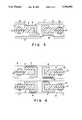
- FIGS. 1-5are schematic diagrams illustrating the method of the present invention.
- FIG. 1illustrates a subcomposite assembly to be connected pursuant to the present invention.
- the subcomposite 1comprises a dielectric substrate 2 and metallic electrical contact pads 3 and vias 4.
- the term viasis normally used to describe conductive pathways within the circuit board which connect adjacent conductive layers.
- the term through-holeis normally used to describe vias that extend to non-adjacent conductive layers.
- the term blind viais sometimes used to refer to a through-hole which terminates internally. For the sake of brevity, the term through-hole may hereafter be used to refer to both.
- Vias 4includes electrical conductive layer 5 which in the example shown is the same as that which that forms the electrical contact pads 3. According to preferred aspects of the present invention such is copper and is typically about 0.2 to about 1 and more typically about 0.25 to about 0.5 mils thick.
- the vias 4provide for electrical communication between conducting layers.
- Dielectric substrates including thermoplastic thermosetting resinsmay be employed in accordance with the present invention.
- thermosetting polymeric materialsinclude epoxy, phenolic based materials, and polyamides.
- phenolic type materialsinclude copolymers of phenol, resorcinol, and cresol.
- suitable thermoplastic polymeric materialsinclude polyolefins such as polypropylene, polysulfones, polycarbonates, nitrile rubbers, ABS polymers, and fluorocarbon polymers such as polytetrafluoroethylene, polymers of chlorotrifluoroethylene, fluorinated ethylenepropylene polymers, polyvinylidene fluoride and polyhexafluoropropylene.
- the dielectric materialsmay be molded articles of the polymers containing fillers and/or reinforcing agents such as glass filled polymers.
- the dielectric substrate 2is a material having a dielectric constant (ER) of about 3.2 or less in order to reduce signal propagation delays and reduce signal noise and attenuation.
- ERdielectric constant
- a dielectric constant of 3.2 or lessalso permits reduction in signal-to-power spacings.
- Suitable materials which can be used to provide a dielectric constant of 3.2 or lessinclude fluorocarbon polymers such as for example polytetrafluoroethlyene (PTFE), polychlorotrifluoroethylene (CTFE), and polyperfluoropropylene, optionally filled with a filler such as quartz or silicon particles and optionally reinforced with a fabric such as woven fluorocarbon fabric.
- the present inventionis especially advantageous in providing high density, high performance printed circuit boards.
- high densitytypically refers to dimensions of the following approximate values in a printed circuit card or board:
- Packaging chips in a surface mount modecan require wiring densities exceeding several thousand inches per square inch and via densities which can exceed 10,000 vias per square inch for very high I/O chips in close proximity.
- DCAdirect chip attach
- a high density circuit board having the above-mentioned dimensionswould be capable of providing wiring capability of approximately 100 inches per square inch per wiring plane and via densities of about 5,000 to about 10,000 vias per square inch.
- the total wiring requirementwould be satisfied by adding a sufficient number of wiring planes to accommodate the number of chips.
- the small diameter viatypically required precludes building such a high density board through traditional multi-layer lamination and drill processes.
- stacked via methodare used.
- a stacked via boardis a circuit board which is made up of individual 2S1P (two signal planes plus one power plane) units joined at the vias to provide communication between 2S1P units.
- the present inventionis especially suitable for providing 2S1P units and for joining such units to each other.
- the subcomposite illustrated in FIG. 1is for a so-called 2S1P core since it contains two signal planes 10 and 11 and one power plane 12.
- the power plane 12may be comprised, for example, of Invar or copper, or copper clad Invar, or copper clad molybdenum.
- a dielectric material 6is applied above the metallic layers 3 and in through-hole 4 (see FIG. 2).
- the dielectric materialmay or may not be photosensitive and may be either thermoplastic or thermosetting. In either case, the material is processed to thereby expose and provide at least one electrically conductive contact pad or so-called via-land site at which a joining metal connection is desired.
- the materialwould be photo processed to form the cavities by means such as ultraviolet, electron beam or x-ray lithography, depending on the nature of the photosensitive dielectric material.
- the cavitieswould be formed through, for example, laser ablation at the sites where a connection is desired.
- Suitable dielectric materialsinclude fluorocarbon polymeric materials and cyanate resins.
- Suitable photosensitive materialsinclude OPR (Optimized Permanent Resist described in U.S. Pat. No. 4,940,651 issued Jul. 10, 1990 to Brown et al, which is incorporated herein by reference) HTM (High Temperature Mask) described in copending Ser. No. 07/382,311 to Gelorme et al, filed in the United States Patent and Trademark Office on Jul. 20, 1989, incorporated herein by reference, and commonly assigned to the present assignee.
- FIG. 2illustrates the presence of electrically conductive pads on both surfaces of substrate 1. However, it is understood that only one side of the substrate 2 necessarily includes a contact pad. These contact pads are also referred to as lands.
- the dielectric layer 6 at this stage of the processshould not be subjected to final cure conditions.
- the dielectric layer 6is typically about 1 to about 6 mils thick and preferably about 2 to about 3 mils thick.
- the preferred dendritesare from palladium metal which posses the desirable mechanical and physical properties.
- the dendritescover the exposed metallic area of the contact pads.
- One method for providing the dendritesis to apply a photo resist material 7 to the structure and then expose and develop the resist according to known photolithographic techniques to provide the exposed area for the subsequently to be formed dendrites. (See FIG. 3).
- Typical photoresist materialsare methacrylate polymeric resist compositions and electrophoretic resists such as those obtainable from Shipley.
- an intermediate layer of nickelis electroplated onto the thin copper plating followed by an intermediate layer of palladium, after applying resist material 7.
- the nickel layeris typically about 1 to about 2.5 microns and more typically about 2 microns thick.
- the nickelcovers the copper to prevent it from contaminating the palladium plating composition.
- this intermediate layer of palladiumis typically about 1 to about 2.5 microns and more typically about 2 microns thick.
- Typical compositions and parameters for electroplating these layers of nickel and palladiumare disclosed in U.S. patent application Ser. No. 07/606,007, filed Oct. 30, 1990 entitled “Separable Electrical Connection Technology,” disclosure of which is incorporated herein by reference.
- the combined nickel and palladium layersare referred to as numeral 8 in FIG. 3.
- the dendrites 9are then formed on the intermediate palladium layer by any known technique such as by ultrasonic plating of palladium typically at about 80 to 100 milleamps/cm 2 of surface area of contact pad.
- Typical palladium compositionsare disclosed in U.S. patent application Ser. No. 07/606,007 entitled “Separable Electrical Connection Technology,” disclosure of which is incorporated herein by reference. It is preferred that the dendrites are about 0.5 to about 1 mil in height.
- each of the dendritescan be coated with a metal that could interface with or diffuse to form a metallic bond. For instance one of the dendrites can be coated with pure gold and the corresponding dendrite with tin.
- the photoresist 7is then removed by stripping in a suitable solvent, such as propylene carbonate.
- the subcompositeis contacted with another subcomposite whereby electrical contacts that face each other are contacted (see FIG. 4).
- electrical contact pads on one of the organic polymeric subcompositesis larger than electrical contact pads on the other organic subcomposite. This provides for proper alignment of the subcomposites with each other by providing sufficient tolerance.
- the larger electrical contact pads and therefore larger area covered by dendritesare about 25 percent to about 75 percent larger than the other contact pads and preferably about 30 to about 60 percent larger.
- the padsare typically about 5 mils to about 100 mils wide.
- the subcompositescan be mated initially below the melting point of the organic polymeric material at relatively low temperatures of about 25° C. (normal room temperature) to about 200° C. and then tested to determine whether proper interconnection has been achieved. At this stage of the process, if it is necessary to rework or repair the subcomposites such can be readily separated by physically lifting one off of the other.
- One of the advantages of the present inventionis that the subcomposite interconnection can be tested to determine whether the interconnection has been successfully achieved and if not the subcomposites can be reworked or repaired without discarding the subcomposites.
- the compositecan then be subjected to a final cure and laminating procedure whereby the subcomposites are heated to temperatures typically of at least about 250° C. and more typically of about 250° C. to about 400° C. under pressure of about 100 psi to about 500 psi while the electrical contact pads that face each other are maintained in contact with each other. This heating results in a bonded composite which is then permitted to cool to provide permanent bond of the composites to each other.
- Two polytetrafluoroethylene subcompositeseach having copper contact pads provided with intermediate layers of nickel and palladium followed by palladium dendrites thereon of an average height of 1 mil are provided with the surface area of contact pads of one of the subcomposites being at least 25 percent greater than that of the other composite.
- the palladium dendrites on one of the subcompositesis electroplated with pure gold at a thickness of about 3 to 4 microns.
- the palladium dendrites on the other substrateare electroplated with tin at a thickness of about 1 to 2 microns.
- the gold plated palladium dendritesare then contacted at room temperature with corresponding tin plated palladium dendrites and the assembly is tested for proper alignment.
- the assemblyis laminated by heating to about 310° C. under pressure of about 500 psi which causes the gold and tin to bond together.
- the temperatureis then raised to about 350° C. to about 380° C. at a pressure of about 500 psi resulting in a bond between the polytetrafluoroethylene of the contacting subcomposites.
- the entire heating proceduretakes about 1 hour.
Landscapes
- Engineering & Computer Science (AREA)
- Manufacturing & Machinery (AREA)
- Microelectronics & Electronic Packaging (AREA)
- Production Of Multi-Layered Print Wiring Board (AREA)
Abstract
Description
This application is a continuation-in-part of our co-pending U.S. patent application Ser. No. 07/605,615, now U.S. Pat. No. 5,129,142, filed Oct. 30, 1990 and entitled "Encapsulated Circuitized Power Core Alignment and Lamination," the entire disclosure of which is incorporated herein by reference.
The present invention is concerned with organic circuit boards and to a method for connecting two or more organic polymeric subcomposites for fabricating such circuit boards. In particular, the present invention is concerned with employing metallic dendrites for connecting the subcomposites to each other. The present invention is especially advantageous in providing high density, high performance printed circuit boards.
Although there has been considerable activity in printed circuit board technology, high density printed circuitry is a relatively recent area of investigation. Only recently have materials and processes been developed which can be used to provide the demanding electrical mechanical properties required by high density configurations. High density packaging configurations are required in order to furnish fast access to large amounts of data in the next generation of computers, such as in supercomputers. Conventional packaging techniques will not meet the requirements of high speed signal processing systems. These sophisticated systems, with millions of circuit devices operate at cycle times in the range of one nanosecond or faster. At such speeds, present day packaging techniques will not suffice. Gains in processing speeds achieved at the integrated circuit level are lost when signals transfer between packaging levels and are required to travel long distances. Conventional packages will not permit signal propagation between chip and package without severe loss, distortion, cross-talk, and/or delay.
New packaging approaches, with the ways to package integrated circuits more efficiently, are required to meet this need.
A further challenge posed by the tremendous increase in circuit density on the chip is the power requirements of the package. Better packaging is achieved by increasing the package density, by reducing the thickness of the package including the power and reference planes. However, to meet power requirements, a greater amount of conductor is required. This dichotomy is resolved by creating a separate power board that is then attached to the signal board/chip carrier. When the chip carrier is a ceramic or glass/ceramic MCM, the attachment can be facilitated by a combination of braised pins on the MCM and harcorn springs in the board. However, surface mounted pins that can withstand the stresses of insertion are not possible when both the chip carrier and board substrate are made from an organic polymeric material. Accordingly, an objective of the present invention is to provide an attachment process for connecting two or more organic polymeric substrates.
In circuit boards which do not have the stringent dimensional requirements of high density circuit boards, alignment of through holes from layer to layer is made indirectly, by aligning mechanical location slots which are peripheral to the function of the device and are placed over locating pins in order to align multiple layers. However, in high density circuit boards, the denser circuitry, finer conductor line and track width, thinner dielectric layers, greater number of layers and denser placement of smaller diameter holes and vias require an absolute, dead-on alignment from layer to layer that is not attainable through means that were satisfactory in the past. In the high density circuitry of the future, through-hole tolerance is such that a small misalignment can mean that there is no electrical interconnection at all, or a high resistance interconnection, between the layers where low resistance is required. The alignment of wire cores to each other is thus seen to be a very demanding registration operation requiring optical registration at the key registration step, viz. drilling, exposing circuitry, laminating layers together. This alignment is currently verified by means of attachment coupled with x-ray examination.
The present invention reduces the need for x-ray verification of alignment since alignment can be verified electrically on a subcomposite level.
It is an object of the invention to produce a high density circuit board device exhibiting interlayer alignment and electrical communication.
The present invention is concerned with a method for interconnecting at least two organic polymeric substrates to each other and especially concerned with at least two organic polymeric subcomposites of a circuit board together. The method of the present invention provides for a certain degree of hermeticity whereby the interconnection is protected from environmental contamination such as from dust, perspiration, oxidation and wear caused by vibration and normal contact service.
In particular, the present invention is concerned with a method for connecting two or more organic polymeric subcomposites of a circuit board. The method includes providing metallic dendrites on electrical contact pads of the two organic polymeric subcomposites. The electrical contact pads of one of the subcomposites face electrical contact pads of the other of the organic polymeric subcomposites. In addition, electrical contact pad on one of the subcomposites is larger than the corresponding electrical contact pad it faces on the other subcomposite. The electrical contact pads having the metallic dendrites thereon are contacted with opposing facing electrical contact pads of the other subcomposite having dendrites thereon. At this stage, if desired, the structure can be tested for continuity and/or alignment. The subcomposites are then heated while the electrical contact pads that face each other are in contact with each other to thereby thermally reflow the polymeric organic material of the subcomposites and form a bonded composite. The bonded composite is then permitted to cool to thereby provide the bonding of the subcomposites.
The present invention is also concerned with a bonded composite obtained by the above-disclosed method. A further aspect of the present invention is concerned with an integrated circuit board that comprises at least two organic polymeric subcomposites wherein the subcomposites are bonded to each other by metallic dendrites on electrical contact pads of the subcomposites. The electrical contact pads of one of the organic polymeric subcomposites face electrical contact pads of the other of the organic subcomposites. Moreover, an electrical contact pad on one of the subcomposites is larger than the corresponding electrical contact pad it faces on the other subcomposite.
FIGS. 1-5 are schematic diagrams illustrating the method of the present invention.
In order to facilitate an understanding of the present invention, reference is made to the Figures. In particular, FIG. 1 illustrates a subcomposite assembly to be connected pursuant to the present invention. The subcomposite 1 comprises adielectric substrate 2 and metallicelectrical contact pads 3 andvias 4. The term vias is normally used to describe conductive pathways within the circuit board which connect adjacent conductive layers. The term through-hole is normally used to describe vias that extend to non-adjacent conductive layers. The term blind via is sometimes used to refer to a through-hole which terminates internally. For the sake of brevity, the term through-hole may hereafter be used to refer to both.Vias 4 includes electricalconductive layer 5 which in the example shown is the same as that which that forms theelectrical contact pads 3. According to preferred aspects of the present invention such is copper and is typically about 0.2 to about 1 and more typically about 0.25 to about 0.5 mils thick. Thevias 4 provide for electrical communication between conducting layers.
Dielectric substrates including thermoplastic thermosetting resins, may be employed in accordance with the present invention.
Typical thermosetting polymeric materials include epoxy, phenolic based materials, and polyamides. Examples of some phenolic type materials include copolymers of phenol, resorcinol, and cresol. Examples of some suitable thermoplastic polymeric materials include polyolefins such as polypropylene, polysulfones, polycarbonates, nitrile rubbers, ABS polymers, and fluorocarbon polymers such as polytetrafluoroethylene, polymers of chlorotrifluoroethylene, fluorinated ethylenepropylene polymers, polyvinylidene fluoride and polyhexafluoropropylene. The dielectric materials may be molded articles of the polymers containing fillers and/or reinforcing agents such as glass filled polymers.
According to preferred aspects of the present invention, thedielectric substrate 2 is a material having a dielectric constant (ER) of about 3.2 or less in order to reduce signal propagation delays and reduce signal noise and attenuation. A dielectric constant of 3.2 or less also permits reduction in signal-to-power spacings. Suitable materials which can be used to provide a dielectric constant of 3.2 or less include fluorocarbon polymers such as for example polytetrafluoroethlyene (PTFE), polychlorotrifluoroethylene (CTFE), and polyperfluoropropylene, optionally filled with a filler such as quartz or silicon particles and optionally reinforced with a fabric such as woven fluorocarbon fabric.
The present invention is especially advantageous in providing high density, high performance printed circuit boards.
In the present invention, the term high density typically refers to dimensions of the following approximate values in a printed circuit card or board:
______________________________________ Line Width 50 Microns (Approx. 2. mils) Line Thickness 12.5 Microns (Approx. 0.5 mils) Via Diameter 63 Microns ±25 Microns (2.5 ± 1.0 mil) Land Diameter 120 Microns (4.7 mils) Clearance Hole 170 Microns (6.7 mils) Core Thickness 127 Microns (5.0 mils) ______________________________________
Packaging chips in a surface mount mode, called also direct chip attach (DCA), can require wiring densities exceeding several thousand inches per square inch and via densities which can exceed 10,000 vias per square inch for very high I/O chips in close proximity.
A high density circuit board having the above-mentioned dimensions would be capable of providing wiring capability of approximately 100 inches per square inch per wiring plane and via densities of about 5,000 to about 10,000 vias per square inch. The total wiring requirement would be satisfied by adding a sufficient number of wiring planes to accommodate the number of chips. The small diameter via typically required precludes building such a high density board through traditional multi-layer lamination and drill processes. In order to produce wiring and via densities of this magnitude, stacked via method are used. A stacked via board is a circuit board which is made up of individual 2S1P (two signal planes plus one power plane) units joined at the vias to provide communication between 2S1P units.
The present invention is especially suitable for providing 2S1P units and for joining such units to each other.
The subcomposite illustrated in FIG. 1 is for a so-called 2S1P core since it contains twosignal planes 10 and 11 and onepower plane 12. Thepower plane 12 may be comprised, for example, of Invar or copper, or copper clad Invar, or copper clad molybdenum.
Next, adielectric material 6 is applied above themetallic layers 3 and in through-hole 4 (see FIG. 2). The dielectric material may or may not be photosensitive and may be either thermoplastic or thermosetting. In either case, the material is processed to thereby expose and provide at least one electrically conductive contact pad or so-called via-land site at which a joining metal connection is desired. In the case of a photosensitive dielectric, the material would be photo processed to form the cavities by means such as ultraviolet, electron beam or x-ray lithography, depending on the nature of the photosensitive dielectric material. In the case of a non-photosensitive dielectric, the cavities would be formed through, for example, laser ablation at the sites where a connection is desired.
Suitable dielectric materials include fluorocarbon polymeric materials and cyanate resins. Suitable photosensitive materials include OPR (Optimized Permanent Resist described in U.S. Pat. No. 4,940,651 issued Jul. 10, 1990 to Brown et al, which is incorporated herein by reference) HTM (High Temperature Mask) described in copending Ser. No. 07/382,311 to Gelorme et al, filed in the United States Patent and Trademark Office on Jul. 20, 1989, incorporated herein by reference, and commonly assigned to the present assignee. FIG. 2 illustrates the presence of electrically conductive pads on both surfaces of substrate 1. However, it is understood that only one side of thesubstrate 2 necessarily includes a contact pad. These contact pads are also referred to as lands. Thedielectric layer 6 at this stage of the process should not be subjected to final cure conditions. Thedielectric layer 6 is typically about 1 to about 6 mils thick and preferably about 2 to about 3 mils thick.
In order to provide enhanced adhesion of subsequently applied layers, it is desirable but not necessary to roughen the surface of the dielectric and exposed electrical contact pads such as by vapor blasting.
Next, metallic dendrites are provided on the electric contact pads. The preferred dendrites are from palladium metal which posses the desirable mechanical and physical properties. The dendrites cover the exposed metallic area of the contact pads. One method for providing the dendrites is to apply a photo resistmaterial 7 to the structure and then expose and develop the resist according to known photolithographic techniques to provide the exposed area for the subsequently to be formed dendrites. (See FIG. 3).
Typical photoresist materials are methacrylate polymeric resist compositions and electrophoretic resists such as those obtainable from Shipley.
According to a preferred method, an intermediate layer of nickel is electroplated onto the thin copper plating followed by an intermediate layer of palladium, after applying resistmaterial 7.
The nickel layer is typically about 1 to about 2.5 microns and more typically about 2 microns thick. The nickel covers the copper to prevent it from contaminating the palladium plating composition.
In addition this intermediate layer of palladium is typically about 1 to about 2.5 microns and more typically about 2 microns thick. Typical compositions and parameters for electroplating these layers of nickel and palladium are disclosed in U.S. patent application Ser. No. 07/606,007, filed Oct. 30, 1990 entitled "Separable Electrical Connection Technology," disclosure of which is incorporated herein by reference.
The combined nickel and palladium layers are referred to as numeral 8 in FIG. 3.
The dendrites 9 (see FIG. 4) are then formed on the intermediate palladium layer by any known technique such as by ultrasonic plating of palladium typically at about 80 to 100 milleamps/cm2 of surface area of contact pad. Typical palladium compositions are disclosed in U.S. patent application Ser. No. 07/606,007 entitled "Separable Electrical Connection Technology," disclosure of which is incorporated herein by reference. It is preferred that the dendrites are about 0.5 to about 1 mil in height. If desired, each of the dendrites can be coated with a metal that could interface with or diffuse to form a metallic bond. For instance one of the dendrites can be coated with pure gold and the corresponding dendrite with tin.
Thephotoresist 7 is then removed by stripping in a suitable solvent, such as propylene carbonate.
Next, the subcomposite is contacted with another subcomposite whereby electrical contacts that face each other are contacted (see FIG. 4). It is essential to the success of the present invention, that electrical contact pads on one of the organic polymeric subcomposites is larger than electrical contact pads on the other organic subcomposite. This provides for proper alignment of the subcomposites with each other by providing sufficient tolerance. Typically the larger electrical contact pads and therefore larger area covered by dendrites are about 25 percent to about 75 percent larger than the other contact pads and preferably about 30 to about 60 percent larger. The pads are typically about 5 mils to about 100 mils wide.
The subcomposites can be mated initially below the melting point of the organic polymeric material at relatively low temperatures of about 25° C. (normal room temperature) to about 200° C. and then tested to determine whether proper interconnection has been achieved. At this stage of the process, if it is necessary to rework or repair the subcomposites such can be readily separated by physically lifting one off of the other. One of the advantages of the present invention is that the subcomposite interconnection can be tested to determine whether the interconnection has been successfully achieved and if not the subcomposites can be reworked or repaired without discarding the subcomposites.
Once the interconnections have passed the quality testing, the composite can then be subjected to a final cure and laminating procedure whereby the subcomposites are heated to temperatures typically of at least about 250° C. and more typically of about 250° C. to about 400° C. under pressure of about 100 psi to about 500 psi while the electrical contact pads that face each other are maintained in contact with each other. This heating results in a bonded composite which is then permitted to cool to provide permanent bond of the composites to each other.
The following non-limiting example is presented to further illustrate the present invention:
Two polytetrafluoroethylene subcomposites each having copper contact pads provided with intermediate layers of nickel and palladium followed by palladium dendrites thereon of an average height of 1 mil are provided with the surface area of contact pads of one of the subcomposites being at least 25 percent greater than that of the other composite. The palladium dendrites on one of the subcomposites is electroplated with pure gold at a thickness of about 3 to 4 microns. The palladium dendrites on the other substrate are electroplated with tin at a thickness of about 1 to 2 microns.
The gold plated palladium dendrites are then contacted at room temperature with corresponding tin plated palladium dendrites and the assembly is tested for proper alignment.
Next the assembly is laminated by heating to about 310° C. under pressure of about 500 psi which causes the gold and tin to bond together. The temperature is then raised to about 350° C. to about 380° C. at a pressure of about 500 psi resulting in a bond between the polytetrafluoroethylene of the contacting subcomposites. The entire heating procedure takes about 1 hour.
Claims (10)
1. A bonded composite of at least two organic polymeric subcomposites of a circuit board obtained by
(a) providing metallic dendrites on electrical contact pads of said two organic polymeric subcomposites wherein electrical contact pads of one of said organic polymeric subcomposites face electrical contact pads of the other of said organic subcompsites; and wherein an electrical contact pad on one of the subcomposites is larger than the electrical contact pad it faces on the other subcomposite;
(b) contacting the electrical contact pads that face each other;
(c) heating said subcomposites while the said electrical contact pads that face each other are in contact with each other to form a bonded composite;
(d) and then permitting said bonded composite to cool.
2. An integrated circuit board comprising at least two organic polymeric subcomposites wherein said subcomposites are bonded to each other by metallic dendrites on electrical contact pads of said subcomposites, wherein electrical contact pads of one of said organic polymeric subcomposites face electrical contact pads of the other of said organic subcomposites; and wherein an electrical contact pad on one of the subcomposites is larger than the electrical contact pad it faces on the other subcomposite.
3. The circuit board of claim 2 wherein said dendrites are palladium.
4. The circuit board of claim 2 wherein the larger of the electrical contact pads is about 25 percent to about 75 percent larger widthwise as compared to the other of the electrical contact pads.
5. The circuit board of claim 2 wherein the height of said dendrites is about 0.5 mil to about 1 mil.
6. The circuit board of claim 2 wherein said electrical contact pads are copper.
7. The circuit board of claim 2 wherein said contact pads are about 5 mils to about 100 mils wide.
8. The circuit board of claim 3 wherein the dendrites on corresponding subcomposites are coated with a metal that is capable of bonding with each other.
9. The circuit board of claim 8 wherein dendrites one of the subcomposites is coated with gold and dendrites on the other subcomposite is coated with tin.
10. The composite of claim 1 wherein said subcomposites prior to said heating are at a temperature of about 25° C. to about 200° C. and below the melting point of the organic polymeric material of said subcomposites to provide a temporary bond.
Priority Applications (3)
| Application Number | Priority Date | Filing Date | Title |
|---|---|---|---|
| US07/913,086US5298685A (en) | 1990-10-30 | 1992-07-14 | Interconnection method and structure for organic circuit boards |
| PCT/US1993/006640WO1994001984A1 (en) | 1992-07-14 | 1993-07-14 | Interconnection method and structure for organic circuit boards |
| US08/195,174US5435057A (en) | 1990-10-30 | 1994-02-14 | Interconnection method and structure for organic circuit boards |
Applications Claiming Priority (2)
| Application Number | Priority Date | Filing Date | Title |
|---|---|---|---|
| US07/605,615US5129142A (en) | 1990-10-30 | 1990-10-30 | Encapsulated circuitized power core alignment and lamination |
| US07/913,086US5298685A (en) | 1990-10-30 | 1992-07-14 | Interconnection method and structure for organic circuit boards |
Related Parent Applications (1)
| Application Number | Title | Priority Date | Filing Date |
|---|---|---|---|
| US07/605,615Continuation-In-PartUS5129142A (en) | 1990-10-30 | 1990-10-30 | Encapsulated circuitized power core alignment and lamination |
Related Child Applications (1)
| Application Number | Title | Priority Date | Filing Date |
|---|---|---|---|
| US08/195,174DivisionUS5435057A (en) | 1990-10-30 | 1994-02-14 | Interconnection method and structure for organic circuit boards |
Publications (1)
| Publication Number | Publication Date |
|---|---|
| US5298685Atrue US5298685A (en) | 1994-03-29 |
Family
ID=25432915
Family Applications (2)
| Application Number | Title | Priority Date | Filing Date |
|---|---|---|---|
| US07/913,086Expired - Fee RelatedUS5298685A (en) | 1990-10-30 | 1992-07-14 | Interconnection method and structure for organic circuit boards |
| US08/195,174Expired - Fee RelatedUS5435057A (en) | 1990-10-30 | 1994-02-14 | Interconnection method and structure for organic circuit boards |
Family Applications After (1)
| Application Number | Title | Priority Date | Filing Date |
|---|---|---|---|
| US08/195,174Expired - Fee RelatedUS5435057A (en) | 1990-10-30 | 1994-02-14 | Interconnection method and structure for organic circuit boards |
Country Status (2)
| Country | Link |
|---|---|
| US (2) | US5298685A (en) |
| WO (1) | WO1994001984A1 (en) |
Cited By (40)
| Publication number | Priority date | Publication date | Assignee | Title |
|---|---|---|---|---|
| US5373111A (en)* | 1993-11-19 | 1994-12-13 | Delco Electronics Corporation | Bond pad having a patterned bonding surface |
| US5709336A (en)* | 1996-05-31 | 1998-01-20 | International Business Machines Corporation | Method of forming a solderless electrical connection with a wirebond chip |
| US5939786A (en)* | 1996-11-08 | 1999-08-17 | International Business Machines Corporation | Uniform plating of dendrites |
| US5977642A (en)* | 1997-08-25 | 1999-11-02 | International Business Machines Corporation | Dendrite interconnect for planarization and method for producing same |
| US6077090A (en)* | 1997-06-10 | 2000-06-20 | International Business Machines Corporation | Flexible circuit connector with floating alignment frame |
| US6167948B1 (en) | 1996-11-18 | 2001-01-02 | Novel Concepts, Inc. | Thin, planar heat spreader |
| US6175087B1 (en)* | 1998-12-02 | 2001-01-16 | International Business Machines Corporation | Composite laminate circuit structure and method of forming the same |
| US6176985B1 (en) | 1998-10-23 | 2001-01-23 | International Business Machines Corporation | Laminated electroplating rack and connection system for optimized plating |
| US6204453B1 (en)* | 1998-12-02 | 2001-03-20 | International Business Machines Corporation | Two signal one power plane circuit board |
| US6224396B1 (en) | 1997-07-23 | 2001-05-01 | International Business Machines Corporation | Compliant, surface-mountable interposer |
| US6256874B1 (en)* | 1997-08-25 | 2001-07-10 | International Business Machines Corporation | Conductor interconnect with dendrites through film and method for producing same |
| US6518516B2 (en) | 2000-04-25 | 2003-02-11 | International Business Machines Corporation | Multilayered laminate |
| US20030140490A1 (en)* | 2001-03-08 | 2003-07-31 | Olson Kevin C. | Multi-layer circuit assembly and process for preparing the same |
| WO2002073685A3 (en)* | 2001-03-08 | 2003-10-16 | Ppg Ind Ohio Inc | Multi-layer circuit assembly and process for preparing the same |
| US20040000049A1 (en)* | 2001-03-08 | 2004-01-01 | Mccollum Gregory J. | Process for fabricating circuit assemblies using electrodepositable dielectric coating compositions |
| US6759596B1 (en)* | 2000-05-12 | 2004-07-06 | Shipley Company | Sequential build circuit board |
| US20040183182A1 (en)* | 2002-01-23 | 2004-09-23 | Susan Swindlehurst | Apparatus incorporating small-feature-size and large-feature-size components and method for making same |
| US20040188531A1 (en)* | 2003-03-24 | 2004-09-30 | Gengel Glenn W. | RFID tags and processes for producing RFID tags |
| US6824959B2 (en) | 2002-06-27 | 2004-11-30 | Ppg Industries Ohio, Inc. | Process for creating holes in polymeric substrates |
| US6832436B2 (en) | 2000-04-25 | 2004-12-21 | International Business Machines Corporation | Method for forming a substructure of a multilayered laminate |
| US20050006138A1 (en)* | 2002-06-27 | 2005-01-13 | Wang Alan E. | Single or multi-layer printed circuit board with recessed or extended breakaway tabs and method of manufacture thereof |
| US20050121225A1 (en)* | 2003-12-03 | 2005-06-09 | Phoenix Precision Technology Corporation | Multi-layer circuit board and method for fabricating the same |
| US20050270757A1 (en)* | 2001-05-31 | 2005-12-08 | Credelle Thomas L | Electronic devices with small functional elements supported on a carrier |
| US20060109129A1 (en)* | 2004-11-22 | 2006-05-25 | Curt Carrender | Transponder incorporated into an electronic device |
| US20060109130A1 (en)* | 2004-11-22 | 2006-05-25 | Hattick John B | Radio frequency identification (RFID) tag for an item having a conductive layer included or attached |
| US20060109123A1 (en)* | 2004-11-22 | 2006-05-25 | Curt Carrender | Radio frequency identification (RFID) tag for an item having a conductive layer included or attached |
| US20060148166A1 (en)* | 2004-11-08 | 2006-07-06 | Craig Gordon S | Assembly comprising functional devices and method of making same |
| US20060213685A1 (en)* | 2002-06-27 | 2006-09-28 | Wang Alan E | Single or multi-layer printed circuit board with improved edge via design |
| US7288432B2 (en) | 1999-03-16 | 2007-10-30 | Alien Technology Corporation | Electronic devices with small functional elements supported on a carrier |
| US20070293038A1 (en)* | 2002-04-02 | 2007-12-20 | Sony Corporation | Method of manufacturing multilayer wiring substrate, and multilayer wiring substrate |
| US7348492B1 (en)* | 1999-11-17 | 2008-03-25 | Sharp Kabushiki Kaisha | Flexible wiring board and electrical device using the same |
| US7452748B1 (en) | 2004-11-08 | 2008-11-18 | Alien Technology Corporation | Strap assembly comprising functional block deposited therein and method of making same |
| US7542301B1 (en) | 2005-06-22 | 2009-06-02 | Alien Technology Corporation | Creating recessed regions in a substrate and assemblies having such recessed regions |
| US7551141B1 (en) | 2004-11-08 | 2009-06-23 | Alien Technology Corporation | RFID strap capacitively coupled and method of making same |
| EP2200414A3 (en)* | 2008-12-03 | 2011-10-26 | Thales Holdings UK Plc | Integrated circuit package |
| US8065795B2 (en) | 2001-03-08 | 2011-11-29 | Ppg Industries Ohio, Inc | Multi-layer circuit assembly and process for preparing the same |
| US20120297618A1 (en)* | 2009-03-14 | 2012-11-29 | Palo Alto Research Center Incorporated | Printed circuit boards by massive parallel assembly |
| CN103077936A (en)* | 2011-10-25 | 2013-05-01 | 日本特殊陶业株式会社 | Wiring substrate and manufacturing method of the same |
| US20170352847A1 (en)* | 2016-06-07 | 2017-12-07 | Robert Bosch Gmbh | Circuit board and charging device including a circuit board for a rechargeable battery pack |
| CN107820363A (en)* | 2017-11-27 | 2018-03-20 | 上海安费诺永亿通讯电子有限公司 | Circuit structure preparation method and circuit structure |
Families Citing this family (135)
| Publication number | Priority date | Publication date | Assignee | Title |
|---|---|---|---|---|
| US5617300A (en)* | 1993-08-23 | 1997-04-01 | Nagano Japan Radio Co., Ltd. | Connecting method of printed substrate and apparatus |
| US5745333A (en)* | 1994-11-21 | 1998-04-28 | International Business Machines Corporation | Laminar stackable circuit board structure with capacitor |
| US5509200A (en)* | 1994-11-21 | 1996-04-23 | International Business Machines Corporation | Method of making laminar stackable circuit board structure |
| EP0713358A3 (en)* | 1994-11-21 | 1997-11-05 | International Business Machines Corporation | Circuit board |
| US5602491A (en)* | 1995-03-16 | 1997-02-11 | Motorola, Inc. | Integrated circuit testing board having constrained thermal expansion characteristics |
| US6061323A (en)* | 1996-07-30 | 2000-05-09 | Seagate Technology, Inc. | Data storage system having an improved surface micro-machined mirror |
| MY128039A (en)* | 1996-12-19 | 2007-01-31 | Ibiden Co Ltd | Printed circuit boards and method of producing the same |
| US6142789A (en)* | 1997-09-22 | 2000-11-07 | Silicon Graphics, Inc. | Demateable, compliant, area array interconnect |
| US7005326B1 (en) | 1998-06-24 | 2006-02-28 | Amkor Technology, Inc. | Method of making an integrated circuit package |
| US7332375B1 (en) | 1998-06-24 | 2008-02-19 | Amkor Technology, Inc. | Method of making an integrated circuit package |
| US7112474B1 (en) | 1998-06-24 | 2006-09-26 | Amkor Technology, Inc. | Method of making an integrated circuit package |
| US7030474B1 (en) | 1998-06-24 | 2006-04-18 | Amkor Technology, Inc. | Plastic integrated circuit package and method and leadframe for making the package |
| US7071541B1 (en) | 1998-06-24 | 2006-07-04 | Amkor Technology, Inc. | Plastic integrated circuit package and method and leadframe for making the package |
| US6893900B1 (en) | 1998-06-24 | 2005-05-17 | Amkor Technology, Inc. | Method of making an integrated circuit package |
| US6143981A (en) | 1998-06-24 | 2000-11-07 | Amkor Technology, Inc. | Plastic integrated circuit package and method and leadframe for making the package |
| US6281568B1 (en) | 1998-10-21 | 2001-08-28 | Amkor Technology, Inc. | Plastic integrated circuit device package and leadframe having partially undercut leads and die pad |
| US6448633B1 (en) | 1998-11-20 | 2002-09-10 | Amkor Technology, Inc. | Semiconductor package and method of making using leadframe having lead locks to secure leads to encapsulant |
| US6274927B1 (en) | 1999-06-03 | 2001-08-14 | Amkor Technology, Inc. | Plastic package for an optical integrated circuit device and method of making |
| US6077766A (en)* | 1999-06-25 | 2000-06-20 | International Business Machines Corporation | Variable thickness pads on a substrate surface |
| KR100526844B1 (en)* | 1999-10-15 | 2005-11-08 | 앰코 테크놀로지 코리아 주식회사 | semiconductor package and its manufacturing method |
| KR100379089B1 (en) | 1999-10-15 | 2003-04-08 | 앰코 테크놀로지 코리아 주식회사 | leadframe and semiconductor package using it |
| KR20010037247A (en) | 1999-10-15 | 2001-05-07 | 마이클 디. 오브라이언 | Semiconductor package |
| KR100403142B1 (en)* | 1999-10-15 | 2003-10-30 | 앰코 테크놀로지 코리아 주식회사 | semiconductor package |
| US6580159B1 (en) | 1999-11-05 | 2003-06-17 | Amkor Technology, Inc. | Integrated circuit device packages and substrates for making the packages |
| US20070176287A1 (en)* | 1999-11-05 | 2007-08-02 | Crowley Sean T | Thin integrated circuit device packages for improved radio frequency performance |
| US6847103B1 (en) | 1999-11-09 | 2005-01-25 | Amkor Technology, Inc. | Semiconductor package with exposed die pad and body-locking leadframe |
| US6476478B1 (en) | 1999-11-12 | 2002-11-05 | Amkor Technology, Inc. | Cavity semiconductor package with exposed leads and die pad |
| US6639308B1 (en)* | 1999-12-16 | 2003-10-28 | Amkor Technology, Inc. | Near chip size semiconductor package |
| KR100421774B1 (en) | 1999-12-16 | 2004-03-10 | 앰코 테크놀로지 코리아 주식회사 | semiconductor package and its manufacturing method |
| US6320251B1 (en) | 2000-01-18 | 2001-11-20 | Amkor Technology, Inc. | Stackable package for an integrated circuit |
| US6404046B1 (en) | 2000-02-03 | 2002-06-11 | Amkor Technology, Inc. | Module of stacked integrated circuit packages including an interposer |
| KR100559664B1 (en) | 2000-03-25 | 2006-03-10 | 앰코 테크놀로지 코리아 주식회사 | Semiconductor Package |
| KR100583494B1 (en)* | 2000-03-25 | 2006-05-24 | 앰코 테크놀로지 코리아 주식회사 | Semiconductor Package |
| US7042068B2 (en) | 2000-04-27 | 2006-05-09 | Amkor Technology, Inc. | Leadframe and semiconductor package made using the leadframe |
| US6424031B1 (en) | 2000-05-08 | 2002-07-23 | Amkor Technology, Inc. | Stackable package with heat sink |
| US6518659B1 (en) | 2000-05-08 | 2003-02-11 | Amkor Technology, Inc. | Stackable package having a cavity and a lid for an electronic device |
| US6667544B1 (en) | 2000-06-30 | 2003-12-23 | Amkor Technology, Inc. | Stackable package having clips for fastening package and tool for opening clips |
| US6388204B1 (en) | 2000-08-29 | 2002-05-14 | International Business Machines Corporation | Composite laminate circuit structure and methods of interconnecting the same |
| US6931723B1 (en) | 2000-09-19 | 2005-08-23 | International Business Machines Corporation | Organic dielectric electronic interconnect structures and method for making |
| KR20020058209A (en) | 2000-12-29 | 2002-07-12 | 마이클 디. 오브라이언 | Semiconductor package |
| KR100731007B1 (en)* | 2001-01-15 | 2007-06-22 | 앰코 테크놀로지 코리아 주식회사 | Stacked Semiconductor Packages |
| KR100394030B1 (en)* | 2001-01-15 | 2003-08-06 | 앰코 테크놀로지 코리아 주식회사 | stack-type semiconductor package |
| US6605865B2 (en) | 2001-03-19 | 2003-08-12 | Amkor Technology, Inc. | Semiconductor package with optimized leadframe bonding strength |
| US6967395B1 (en) | 2001-03-20 | 2005-11-22 | Amkor Technology, Inc. | Mounting for a package containing a chip |
| US6545345B1 (en) | 2001-03-20 | 2003-04-08 | Amkor Technology, Inc. | Mounting for a package containing a chip |
| KR100393448B1 (en) | 2001-03-27 | 2003-08-02 | 앰코 테크놀로지 코리아 주식회사 | Semiconductor package and method for manufacturing the same |
| KR100369393B1 (en) | 2001-03-27 | 2003-02-05 | 앰코 테크놀로지 코리아 주식회사 | Lead frame and semiconductor package using it and its manufacturing method |
| US6879492B2 (en)* | 2001-03-28 | 2005-04-12 | International Business Machines Corporation | Hyperbga buildup laminate |
| US7045883B1 (en) | 2001-04-04 | 2006-05-16 | Amkor Technology, Inc. | Thermally enhanced chip scale lead on chip semiconductor package and method of making same |
| US7064009B1 (en) | 2001-04-04 | 2006-06-20 | Amkor Technology, Inc. | Thermally enhanced chip scale lead on chip semiconductor package and method of making same |
| US6756658B1 (en) | 2001-04-06 | 2004-06-29 | Amkor Technology, Inc. | Making two lead surface mounting high power microleadframe semiconductor packages |
| US6790710B2 (en) | 2002-01-31 | 2004-09-14 | Asat Limited | Method of manufacturing an integrated circuit package |
| US6861720B1 (en) | 2001-08-29 | 2005-03-01 | Amkor Technology, Inc. | Placement template and method for placing optical dies |
| US7485952B1 (en) | 2001-09-19 | 2009-02-03 | Amkor Technology, Inc. | Drop resistant bumpers for fully molded memory cards |
| US6900527B1 (en) | 2001-09-19 | 2005-05-31 | Amkor Technology, Inc. | Lead-frame method and assembly for interconnecting circuits within a circuit module |
| US6611047B2 (en) | 2001-10-12 | 2003-08-26 | Amkor Technology, Inc. | Semiconductor package with singulation crease |
| US6630726B1 (en) | 2001-11-07 | 2003-10-07 | Amkor Technology, Inc. | Power semiconductor package with strap |
| US6798046B1 (en) | 2002-01-22 | 2004-09-28 | Amkor Technology, Inc. | Semiconductor package including ring structure connected to leads with vertically downset inner ends |
| US6784534B1 (en) | 2002-02-06 | 2004-08-31 | Amkor Technology, Inc. | Thin integrated circuit package having an optically transparent window |
| US6885086B1 (en) | 2002-03-05 | 2005-04-26 | Amkor Technology, Inc. | Reduced copper lead frame for saw-singulated chip package |
| US6608366B1 (en) | 2002-04-15 | 2003-08-19 | Harry J. Fogelson | Lead frame with plated end leads |
| US6627977B1 (en) | 2002-05-09 | 2003-09-30 | Amkor Technology, Inc. | Semiconductor package including isolated ring structure |
| US6841414B1 (en) | 2002-06-19 | 2005-01-11 | Amkor Technology, Inc. | Saw and etch singulation method for a chip package |
| US6867071B1 (en) | 2002-07-12 | 2005-03-15 | Amkor Technology, Inc. | Leadframe including corner leads and semiconductor package using same |
| US6818973B1 (en) | 2002-09-09 | 2004-11-16 | Amkor Technology, Inc. | Exposed lead QFP package fabricated through the use of a partial saw process |
| US6919620B1 (en) | 2002-09-17 | 2005-07-19 | Amkor Technology, Inc. | Compact flash memory card with clamshell leadframe |
| US7723210B2 (en) | 2002-11-08 | 2010-05-25 | Amkor Technology, Inc. | Direct-write wafer level chip scale package |
| US6905914B1 (en) | 2002-11-08 | 2005-06-14 | Amkor Technology, Inc. | Wafer level package and fabrication method |
| US7361533B1 (en) | 2002-11-08 | 2008-04-22 | Amkor Technology, Inc. | Stacked embedded leadframe |
| US7190062B1 (en) | 2004-06-15 | 2007-03-13 | Amkor Technology, Inc. | Embedded leadframe semiconductor package |
| US6798047B1 (en) | 2002-12-26 | 2004-09-28 | Amkor Technology, Inc. | Pre-molded leadframe |
| US6847099B1 (en) | 2003-02-05 | 2005-01-25 | Amkor Technology Inc. | Offset etched corner leads for semiconductor package |
| US6750545B1 (en) | 2003-02-28 | 2004-06-15 | Amkor Technology, Inc. | Semiconductor package capable of die stacking |
| US6927483B1 (en) | 2003-03-07 | 2005-08-09 | Amkor Technology, Inc. | Semiconductor package exhibiting efficient lead placement |
| US6794740B1 (en) | 2003-03-13 | 2004-09-21 | Amkor Technology, Inc. | Leadframe package for semiconductor devices |
| US7001799B1 (en) | 2003-03-13 | 2006-02-21 | Amkor Technology, Inc. | Method of making a leadframe for semiconductor devices |
| US6879034B1 (en) | 2003-05-01 | 2005-04-12 | Amkor Technology, Inc. | Semiconductor package including low temperature co-fired ceramic substrate |
| US7095103B1 (en) | 2003-05-01 | 2006-08-22 | Amkor Technology, Inc. | Leadframe based memory card |
| US7008825B1 (en) | 2003-05-27 | 2006-03-07 | Amkor Technology, Inc. | Leadframe strip having enhanced testability |
| US6897550B1 (en) | 2003-06-11 | 2005-05-24 | Amkor Technology, Inc. | Fully-molded leadframe stand-off feature |
| US7245007B1 (en) | 2003-09-18 | 2007-07-17 | Amkor Technology, Inc. | Exposed lead interposer leadframe package |
| US6921967B2 (en)* | 2003-09-24 | 2005-07-26 | Amkor Technology, Inc. | Reinforced die pad support structure |
| US7138707B1 (en) | 2003-10-21 | 2006-11-21 | Amkor Technology, Inc. | Semiconductor package including leads and conductive posts for providing increased functionality |
| KR100585104B1 (en)* | 2003-10-24 | 2006-05-30 | 삼성전자주식회사 | Manufacturing method of ultra thin flip chip package |
| US6977431B1 (en) | 2003-11-05 | 2005-12-20 | Amkor Technology, Inc. | Stackable semiconductor package and manufacturing method thereof |
| US7144517B1 (en) | 2003-11-07 | 2006-12-05 | Amkor Technology, Inc. | Manufacturing method for leadframe and for semiconductor package using the leadframe |
| US7211879B1 (en) | 2003-11-12 | 2007-05-01 | Amkor Technology, Inc. | Semiconductor package with chamfered corners and method of manufacturing the same |
| US7057268B1 (en) | 2004-01-27 | 2006-06-06 | Amkor Technology, Inc. | Cavity case with clip/plug for use on multi-media card |
| US7091594B1 (en) | 2004-01-28 | 2006-08-15 | Amkor Technology, Inc. | Leadframe type semiconductor package having reduced inductance and its manufacturing method |
| US20080003722A1 (en)* | 2004-04-15 | 2008-01-03 | Chun David D | Transfer mold solution for molded multi-media card |
| US7202554B1 (en) | 2004-08-19 | 2007-04-10 | Amkor Technology, Inc. | Semiconductor package and its manufacturing method |
| US7217991B1 (en) | 2004-10-22 | 2007-05-15 | Amkor Technology, Inc. | Fan-in leadframe semiconductor package |
| US7507603B1 (en) | 2005-12-02 | 2009-03-24 | Amkor Technology, Inc. | Etch singulated semiconductor package |
| US7572681B1 (en) | 2005-12-08 | 2009-08-11 | Amkor Technology, Inc. | Embedded electronic component package |
| US7902660B1 (en) | 2006-05-24 | 2011-03-08 | Amkor Technology, Inc. | Substrate for semiconductor device and manufacturing method thereof |
| US7968998B1 (en) | 2006-06-21 | 2011-06-28 | Amkor Technology, Inc. | Side leaded, bottom exposed pad and bottom exposed lead fusion quad flat semiconductor package |
| US7977774B2 (en) | 2007-07-10 | 2011-07-12 | Amkor Technology, Inc. | Fusion quad flat semiconductor package |
| US7687899B1 (en) | 2007-08-07 | 2010-03-30 | Amkor Technology, Inc. | Dual laminate package structure with embedded elements |
| US7847386B1 (en) | 2007-11-05 | 2010-12-07 | Amkor Technology, Inc. | Reduced size stacked semiconductor package and method of making the same |
| US7956453B1 (en) | 2008-01-16 | 2011-06-07 | Amkor Technology, Inc. | Semiconductor package with patterning layer and method of making same |
| US7768135B1 (en) | 2008-04-17 | 2010-08-03 | Amkor Technology, Inc. | Semiconductor package with fast power-up cycle and method of making same |
| US8125064B1 (en) | 2008-07-28 | 2012-02-28 | Amkor Technology, Inc. | Increased I/O semiconductor package and method of making same |
| US8184453B1 (en) | 2008-07-31 | 2012-05-22 | Amkor Technology, Inc. | Increased capacity semiconductor package |
| US7847392B1 (en) | 2008-09-30 | 2010-12-07 | Amkor Technology, Inc. | Semiconductor device including leadframe with increased I/O |
| US7989933B1 (en) | 2008-10-06 | 2011-08-02 | Amkor Technology, Inc. | Increased I/O leadframe and semiconductor device including same |
| US8008758B1 (en) | 2008-10-27 | 2011-08-30 | Amkor Technology, Inc. | Semiconductor device with increased I/O leadframe |
| US8089145B1 (en) | 2008-11-17 | 2012-01-03 | Amkor Technology, Inc. | Semiconductor device including increased capacity leadframe |
| US8072050B1 (en) | 2008-11-18 | 2011-12-06 | Amkor Technology, Inc. | Semiconductor device with increased I/O leadframe including passive device |
| US7982298B1 (en) | 2008-12-03 | 2011-07-19 | Amkor Technology, Inc. | Package in package semiconductor device |
| US8487420B1 (en) | 2008-12-08 | 2013-07-16 | Amkor Technology, Inc. | Package in package semiconductor device with film over wire |
| US8680656B1 (en) | 2009-01-05 | 2014-03-25 | Amkor Technology, Inc. | Leadframe structure for concentrated photovoltaic receiver package |
| US8058715B1 (en) | 2009-01-09 | 2011-11-15 | Amkor Technology, Inc. | Package in package device for RF transceiver module |
| US8026589B1 (en) | 2009-02-23 | 2011-09-27 | Amkor Technology, Inc. | Reduced profile stackable semiconductor package |
| US7960818B1 (en) | 2009-03-04 | 2011-06-14 | Amkor Technology, Inc. | Conformal shield on punch QFN semiconductor package |
| US8575742B1 (en) | 2009-04-06 | 2013-11-05 | Amkor Technology, Inc. | Semiconductor device with increased I/O leadframe including power bars |
| US8796561B1 (en) | 2009-10-05 | 2014-08-05 | Amkor Technology, Inc. | Fan out build up substrate stackable package and method |
| US8937381B1 (en) | 2009-12-03 | 2015-01-20 | Amkor Technology, Inc. | Thin stackable package and method |
| US9691734B1 (en) | 2009-12-07 | 2017-06-27 | Amkor Technology, Inc. | Method of forming a plurality of electronic component packages |
| US8324511B1 (en) | 2010-04-06 | 2012-12-04 | Amkor Technology, Inc. | Through via nub reveal method and structure |
| US8294276B1 (en) | 2010-05-27 | 2012-10-23 | Amkor Technology, Inc. | Semiconductor device and fabricating method thereof |
| US8440554B1 (en) | 2010-08-02 | 2013-05-14 | Amkor Technology, Inc. | Through via connected backside embedded circuit features structure and method |
| US8487445B1 (en) | 2010-10-05 | 2013-07-16 | Amkor Technology, Inc. | Semiconductor device having through electrodes protruding from dielectric layer |
| US8791501B1 (en) | 2010-12-03 | 2014-07-29 | Amkor Technology, Inc. | Integrated passive device structure and method |
| US8674485B1 (en) | 2010-12-08 | 2014-03-18 | Amkor Technology, Inc. | Semiconductor device including leadframe with downsets |
| US8390130B1 (en) | 2011-01-06 | 2013-03-05 | Amkor Technology, Inc. | Through via recessed reveal structure and method |
| TWI557183B (en) | 2015-12-16 | 2016-11-11 | 財團法人工業技術研究院 | Oxane composition, and photovoltaic device comprising the same |
| US8648450B1 (en) | 2011-01-27 | 2014-02-11 | Amkor Technology, Inc. | Semiconductor device including leadframe with a combination of leads and lands |
| US8552548B1 (en) | 2011-11-29 | 2013-10-08 | Amkor Technology, Inc. | Conductive pad on protruding through electrode semiconductor device |
| US9704725B1 (en) | 2012-03-06 | 2017-07-11 | Amkor Technology, Inc. | Semiconductor device with leadframe configured to facilitate reduced burr formation |
| US9048298B1 (en) | 2012-03-29 | 2015-06-02 | Amkor Technology, Inc. | Backside warpage control structure and fabrication method |
| US9129943B1 (en) | 2012-03-29 | 2015-09-08 | Amkor Technology, Inc. | Embedded component package and fabrication method |
| KR101486790B1 (en) | 2013-05-02 | 2015-01-28 | 앰코 테크놀로지 코리아 주식회사 | Micro Lead Frame for semiconductor package |
| KR101563911B1 (en) | 2013-10-24 | 2015-10-28 | 앰코 테크놀로지 코리아 주식회사 | Semiconductor package |
| US9673122B2 (en) | 2014-05-02 | 2017-06-06 | Amkor Technology, Inc. | Micro lead frame structure having reinforcing portions and method |
| CN114126225B (en)* | 2020-08-31 | 2024-12-17 | 庆鼎精密电子(淮安)有限公司 | Method for manufacturing circuit board, circuit board and method for manufacturing circuit board |
Citations (26)
| Publication number | Priority date | Publication date | Assignee | Title |
|---|---|---|---|---|
| US1155427A (en)* | 1914-11-20 | 1915-10-05 | Independent Lamp And Wire Company Inc | Contact bodies of tungsten. |
| US2461980A (en)* | 1946-12-20 | 1949-02-15 | Gen Electric | Electric contact device |
| US2576528A (en)* | 1948-08-07 | 1951-11-27 | Burndy Engineering Co Inc | Connector with hard particle lining |
| US3157735A (en)* | 1961-06-27 | 1964-11-17 | Aluminum Co Of America | Metallic particle compositions for mechanically joined electrical conductors |
| US3239597A (en)* | 1963-09-16 | 1966-03-08 | Honeywell Inc | Self-repair circuit apparatus |
| US3254189A (en)* | 1961-05-15 | 1966-05-31 | Westinghouse Electric Corp | Electrical contact members having a plurality of refractory metal fibers embedded therein |
| US3526867A (en)* | 1967-07-17 | 1970-09-01 | Keeler Brass Co | Interlocking electrical connector |
| US3725844A (en)* | 1971-03-15 | 1973-04-03 | Bendix Corp | Hermaphroditic electrical contact |
| DE2151683A1 (en)* | 1971-10-13 | 1973-04-19 | Siemens Ag | ELECTRICAL CONTACT ARRANGEMENT |
| US3795047A (en)* | 1972-06-15 | 1974-03-05 | Ibm | Electrical interconnect structuring for laminate assemblies and fabricating methods therefor |
| US3818415A (en)* | 1973-02-16 | 1974-06-18 | Amp Inc | Electrical connections to conductors having thin film insulation |
| US3839727A (en)* | 1973-06-25 | 1974-10-01 | Ibm | Semiconductor chip to substrate solder bond using a locally dispersed, ternary intermetallic compound |
| US3934334A (en)* | 1974-04-15 | 1976-01-27 | Texas Instruments Incorporated | Method of fabricating metal printed wiring boards |
| US3984244A (en)* | 1974-11-27 | 1976-10-05 | E. I. Du Pont De Nemours And Company | Process for laminating a channeled photosensitive layer on an irregular surface |
| US4005698A (en)* | 1974-10-18 | 1977-02-01 | International Business Machines Corporation | Photon energy converter |
| CA1121011A (en)* | 1977-04-15 | 1982-03-30 | Robert Babuka | Dendritic electrical contacts and connectors |
| US4383003A (en)* | 1980-09-22 | 1983-05-10 | General Electric Company | Transfer lamination of copper thin sheets and films, method and product |
| US4478883A (en)* | 1982-07-14 | 1984-10-23 | International Business Machines Corporation | Conditioning of a substrate for electroless direct bond plating in holes and on surfaces of a substrate |
| US4551210A (en)* | 1984-11-13 | 1985-11-05 | Olin Corporation | Dendritic treatment of metallic surfaces for improving adhesive bonding |
| US4670770A (en)* | 1984-02-21 | 1987-06-02 | American Telephone And Telegraph Company | Integrated circuit chip-and-substrate assembly |
| US4774122A (en)* | 1986-10-14 | 1988-09-27 | Edward Adler | Resinous product provided with surface coatable with metal layer bonded through an array of microdendrites and metal-clad resinous product thereof |
| US4803450A (en)* | 1987-12-14 | 1989-02-07 | General Electric Company | Multilayer circuit board fabricated from silicon |
| US4830264A (en)* | 1986-10-08 | 1989-05-16 | International Business Machines Corporation | Method of forming solder terminals for a pinless ceramic module |
| JPH01198092A (en)* | 1988-02-03 | 1989-08-09 | Mitsui Mining & Smelting Co Ltd | Printed wiring board having connector function and connection thereof |
| US5019944A (en)* | 1988-08-31 | 1991-05-28 | Mitsui Mining & Smelting Co., Ltd. | Mounting substrate and its production method, and printed wiring board having connector function and its connection method |
| US5105537A (en)* | 1990-10-12 | 1992-04-21 | International Business Machines Corporation | Method for making a detachable electrical contact |
Family Cites Families (1)
| Publication number | Priority date | Publication date | Assignee | Title |
|---|---|---|---|---|
| US3756891A (en)* | 1967-12-26 | 1973-09-04 | Multilayer circuit board techniques |
- 1992
- 1992-07-14USUS07/913,086patent/US5298685A/ennot_activeExpired - Fee Related
- 1993
- 1993-07-14WOPCT/US1993/006640patent/WO1994001984A1/enactiveApplication Filing
- 1994
- 1994-02-14USUS08/195,174patent/US5435057A/ennot_activeExpired - Fee Related
Patent Citations (26)
| Publication number | Priority date | Publication date | Assignee | Title |
|---|---|---|---|---|
| US1155427A (en)* | 1914-11-20 | 1915-10-05 | Independent Lamp And Wire Company Inc | Contact bodies of tungsten. |
| US2461980A (en)* | 1946-12-20 | 1949-02-15 | Gen Electric | Electric contact device |
| US2576528A (en)* | 1948-08-07 | 1951-11-27 | Burndy Engineering Co Inc | Connector with hard particle lining |
| US3254189A (en)* | 1961-05-15 | 1966-05-31 | Westinghouse Electric Corp | Electrical contact members having a plurality of refractory metal fibers embedded therein |
| US3157735A (en)* | 1961-06-27 | 1964-11-17 | Aluminum Co Of America | Metallic particle compositions for mechanically joined electrical conductors |
| US3239597A (en)* | 1963-09-16 | 1966-03-08 | Honeywell Inc | Self-repair circuit apparatus |
| US3526867A (en)* | 1967-07-17 | 1970-09-01 | Keeler Brass Co | Interlocking electrical connector |
| US3725844A (en)* | 1971-03-15 | 1973-04-03 | Bendix Corp | Hermaphroditic electrical contact |
| DE2151683A1 (en)* | 1971-10-13 | 1973-04-19 | Siemens Ag | ELECTRICAL CONTACT ARRANGEMENT |
| US3795047A (en)* | 1972-06-15 | 1974-03-05 | Ibm | Electrical interconnect structuring for laminate assemblies and fabricating methods therefor |
| US3818415A (en)* | 1973-02-16 | 1974-06-18 | Amp Inc | Electrical connections to conductors having thin film insulation |
| US3839727A (en)* | 1973-06-25 | 1974-10-01 | Ibm | Semiconductor chip to substrate solder bond using a locally dispersed, ternary intermetallic compound |
| US3934334A (en)* | 1974-04-15 | 1976-01-27 | Texas Instruments Incorporated | Method of fabricating metal printed wiring boards |
| US4005698A (en)* | 1974-10-18 | 1977-02-01 | International Business Machines Corporation | Photon energy converter |
| US3984244A (en)* | 1974-11-27 | 1976-10-05 | E. I. Du Pont De Nemours And Company | Process for laminating a channeled photosensitive layer on an irregular surface |
| CA1121011A (en)* | 1977-04-15 | 1982-03-30 | Robert Babuka | Dendritic electrical contacts and connectors |
| US4383003A (en)* | 1980-09-22 | 1983-05-10 | General Electric Company | Transfer lamination of copper thin sheets and films, method and product |
| US4478883A (en)* | 1982-07-14 | 1984-10-23 | International Business Machines Corporation | Conditioning of a substrate for electroless direct bond plating in holes and on surfaces of a substrate |
| US4670770A (en)* | 1984-02-21 | 1987-06-02 | American Telephone And Telegraph Company | Integrated circuit chip-and-substrate assembly |
| US4551210A (en)* | 1984-11-13 | 1985-11-05 | Olin Corporation | Dendritic treatment of metallic surfaces for improving adhesive bonding |
| US4830264A (en)* | 1986-10-08 | 1989-05-16 | International Business Machines Corporation | Method of forming solder terminals for a pinless ceramic module |
| US4774122A (en)* | 1986-10-14 | 1988-09-27 | Edward Adler | Resinous product provided with surface coatable with metal layer bonded through an array of microdendrites and metal-clad resinous product thereof |
| US4803450A (en)* | 1987-12-14 | 1989-02-07 | General Electric Company | Multilayer circuit board fabricated from silicon |
| JPH01198092A (en)* | 1988-02-03 | 1989-08-09 | Mitsui Mining & Smelting Co Ltd | Printed wiring board having connector function and connection thereof |
| US5019944A (en)* | 1988-08-31 | 1991-05-28 | Mitsui Mining & Smelting Co., Ltd. | Mounting substrate and its production method, and printed wiring board having connector function and its connection method |
| US5105537A (en)* | 1990-10-12 | 1992-04-21 | International Business Machines Corporation | Method for making a detachable electrical contact |
Non-Patent Citations (11)
| Title |
|---|
| Assembling High Density Printed Circuit Boards, IBM Technical Disclosure Bulletin, vol. 15, No. 1, Jun. 1972.* |
| Assembling High-Density Printed-Circuit Boards, IBM Technical Disclosure Bulletin, vol. 15, No. 1, Jun. 1972. |
| Dendrite Connector System With Reinforced Base, IBM Technical Disclosure Bulletin, vol. 23, No. 8, Jan. 1981.* |
| Dendritic Wick for Heat Pipe Application, IBM Technical Disclosure Bulletin, vol. 14, No. 9, Feb. 1972.* |
| Direct Attachment of a Silicon Carrier for IC Chips to a Circuit Card, vol. 32, No. 4A, Sep. 1989.* |
| Low to High Temperatue Capillary, IBM Technical Disclosure Bulletin, vol. 18, No. 4, Sep. 1975.* |
| Low to High-Temperatue Capillary, IBM Technical Disclosure Bulletin, vol. 18, No. 4, Sep. 1975. |
| Metal Whiskers, by S. M. Arnold, Bell Telephone Laboratories, Inc. Electrical Manufacturing.* |
| Process for Producing Palladium Structures, IBM Technical Disclosure Bulletin, vol. 24, No. 1A, Jun. 1981.* |
| Switches by Michael A. Grundfest, Electronic Design, Sep. 13, 1965, pp. 34 38.* |
| Switches by Michael A. Grundfest, Electronic Design, Sep. 13, 1965, pp. 34-38. |
Cited By (79)
| Publication number | Priority date | Publication date | Assignee | Title |
|---|---|---|---|---|
| US5373111A (en)* | 1993-11-19 | 1994-12-13 | Delco Electronics Corporation | Bond pad having a patterned bonding surface |
| US5709336A (en)* | 1996-05-31 | 1998-01-20 | International Business Machines Corporation | Method of forming a solderless electrical connection with a wirebond chip |
| US5939786A (en)* | 1996-11-08 | 1999-08-17 | International Business Machines Corporation | Uniform plating of dendrites |
| US6043150A (en)* | 1996-11-08 | 2000-03-28 | International Business Machines Corporation | Method for uniform plating of dendrites |
| US6167948B1 (en) | 1996-11-18 | 2001-01-02 | Novel Concepts, Inc. | Thin, planar heat spreader |
| US6077090A (en)* | 1997-06-10 | 2000-06-20 | International Business Machines Corporation | Flexible circuit connector with floating alignment frame |
| US6224396B1 (en) | 1997-07-23 | 2001-05-01 | International Business Machines Corporation | Compliant, surface-mountable interposer |
| US6739046B1 (en) | 1997-08-25 | 2004-05-25 | International Business Machines Corporation | Method for producing dendrite interconnect for planarization |
| US6256874B1 (en)* | 1997-08-25 | 2001-07-10 | International Business Machines Corporation | Conductor interconnect with dendrites through film and method for producing same |
| US6300575B1 (en) | 1997-08-25 | 2001-10-09 | International Business Machines Corporation | Conductor interconnect with dendrites through film |
| KR100304396B1 (en)* | 1997-08-25 | 2001-11-02 | 포만 제프리 엘 | Dendrite interconnect for planarization and method for producing same |
| US6427323B2 (en) | 1997-08-25 | 2002-08-06 | International Business Machines Corporation | Method for producing conductor interconnect with dendrites |
| US5977642A (en)* | 1997-08-25 | 1999-11-02 | International Business Machines Corporation | Dendrite interconnect for planarization and method for producing same |
| US6176985B1 (en) | 1998-10-23 | 2001-01-23 | International Business Machines Corporation | Laminated electroplating rack and connection system for optimized plating |
| US6175087B1 (en)* | 1998-12-02 | 2001-01-16 | International Business Machines Corporation | Composite laminate circuit structure and method of forming the same |
| US6204453B1 (en)* | 1998-12-02 | 2001-03-20 | International Business Machines Corporation | Two signal one power plane circuit board |
| US7288432B2 (en) | 1999-03-16 | 2007-10-30 | Alien Technology Corporation | Electronic devices with small functional elements supported on a carrier |
| US7425467B2 (en) | 1999-03-16 | 2008-09-16 | Alien Technology Corporation | Web process interconnect in electronic assemblies |
| US7348492B1 (en)* | 1999-11-17 | 2008-03-25 | Sharp Kabushiki Kaisha | Flexible wiring board and electrical device using the same |
| US6518516B2 (en) | 2000-04-25 | 2003-02-11 | International Business Machines Corporation | Multilayered laminate |
| US6832436B2 (en) | 2000-04-25 | 2004-12-21 | International Business Machines Corporation | Method for forming a substructure of a multilayered laminate |
| US6759596B1 (en)* | 2000-05-12 | 2004-07-06 | Shipley Company | Sequential build circuit board |
| US20040000049A1 (en)* | 2001-03-08 | 2004-01-01 | Mccollum Gregory J. | Process for fabricating circuit assemblies using electrodepositable dielectric coating compositions |
| WO2002073685A3 (en)* | 2001-03-08 | 2003-10-16 | Ppg Ind Ohio Inc | Multi-layer circuit assembly and process for preparing the same |
| US7228623B2 (en) | 2001-03-08 | 2007-06-12 | Ppg Industries Ohio, Inc. | Process for fabricating a multi layer circuit assembly |
| US8065795B2 (en) | 2001-03-08 | 2011-11-29 | Ppg Industries Ohio, Inc | Multi-layer circuit assembly and process for preparing the same |
| US8598467B2 (en) | 2001-03-08 | 2013-12-03 | PPG Industries Chio, Inc. | Multi-layer circuit assembly and process for preparing the same |
| US20030140490A1 (en)* | 2001-03-08 | 2003-07-31 | Olson Kevin C. | Multi-layer circuit assembly and process for preparing the same |
| US6671950B2 (en) | 2001-03-08 | 2004-01-06 | Ppg Industries Ohio, Inc. | Multi-layer circuit assembly and process for preparing the same |
| US7000313B2 (en) | 2001-03-08 | 2006-02-21 | Ppg Industries Ohio, Inc. | Process for fabricating circuit assemblies using electrodepositable dielectric coating compositions |
| US20050270757A1 (en)* | 2001-05-31 | 2005-12-08 | Credelle Thomas L | Electronic devices with small functional elements supported on a carrier |
| US7559131B2 (en) | 2001-05-31 | 2009-07-14 | Alien Technology Corporation | Method of making a radio frequency identification (RFID) tag |
| US7260882B2 (en) | 2001-05-31 | 2007-08-28 | Alien Technology Corporation | Methods for making electronic devices with small functional elements supported on a carriers |
| US8516683B2 (en) | 2001-05-31 | 2013-08-27 | Alien Technology Corporation | Methods of making a radio frequency identification (RFID) tags |
| US20040183182A1 (en)* | 2002-01-23 | 2004-09-23 | Susan Swindlehurst | Apparatus incorporating small-feature-size and large-feature-size components and method for making same |
| US20070117274A1 (en)* | 2002-01-23 | 2007-05-24 | Susan Swindlehurst | Apparatus incorporating small-feature-size and large-feature-size components and method for making same |
| US7214569B2 (en)* | 2002-01-23 | 2007-05-08 | Alien Technology Corporation | Apparatus incorporating small-feature-size and large-feature-size components and method for making same |
| US20070293038A1 (en)* | 2002-04-02 | 2007-12-20 | Sony Corporation | Method of manufacturing multilayer wiring substrate, and multilayer wiring substrate |
| US7159308B2 (en) | 2002-06-27 | 2007-01-09 | Ppg Industries Ohio, Inc. | Method of making a circuit board |
| US7002081B2 (en) | 2002-06-27 | 2006-02-21 | Ppg Industries Ohio, Inc. | Single or multi-layer printed circuit board with recessed or extended breakaway tabs and method of manufacture thereof |
| US6824959B2 (en) | 2002-06-27 | 2004-11-30 | Ppg Industries Ohio, Inc. | Process for creating holes in polymeric substrates |
| US20050006138A1 (en)* | 2002-06-27 | 2005-01-13 | Wang Alan E. | Single or multi-layer printed circuit board with recessed or extended breakaway tabs and method of manufacture thereof |
| US20060213685A1 (en)* | 2002-06-27 | 2006-09-28 | Wang Alan E | Single or multi-layer printed circuit board with improved edge via design |
| US20060005995A1 (en)* | 2002-06-27 | 2006-01-12 | Wang Alan E | Circuit board and method of manufacture thereof |
| US20060075633A1 (en)* | 2002-06-27 | 2006-04-13 | Wang Alan E | Single or multi-layer printed circuit board with recessed or extended breakaway tabs and method of manufacture thereof |
| WO2004045262A1 (en)* | 2002-11-08 | 2004-05-27 | Ppg Industries Ohio, Inc. | Multi-layer circuit assembly and process for preparing the same |
| US20090167534A1 (en)* | 2003-03-24 | 2009-07-02 | Gengel Glenn W | Rfid tags and processes for producing rfid tags |
| US20040188531A1 (en)* | 2003-03-24 | 2004-09-30 | Gengel Glenn W. | RFID tags and processes for producing RFID tags |
| US7868766B2 (en) | 2003-03-24 | 2011-01-11 | Alien Technology Corporation | RFID tags and processes for producing RFID tags |
| US8912907B2 (en) | 2003-03-24 | 2014-12-16 | Alien Technology, Llc | RFID tags and processes for producing RFID tags |
| US7253735B2 (en) | 2003-03-24 | 2007-08-07 | Alien Technology Corporation | RFID tags and processes for producing RFID tags |
| US7489248B2 (en) | 2003-03-24 | 2009-02-10 | Alien Technology Corporation | RFID tags and processes for producing RFID tags |
| US8350703B2 (en) | 2003-03-24 | 2013-01-08 | Alien Technology Corporation | RFID tags and processes for producing RFID tags |
| US9418328B2 (en) | 2003-03-24 | 2016-08-16 | Ruizhang Technology Limited Company | RFID tags and processes for producing RFID tags |
| US20050121225A1 (en)* | 2003-12-03 | 2005-06-09 | Phoenix Precision Technology Corporation | Multi-layer circuit board and method for fabricating the same |
| US7452748B1 (en) | 2004-11-08 | 2008-11-18 | Alien Technology Corporation | Strap assembly comprising functional block deposited therein and method of making same |
| US7551141B1 (en) | 2004-11-08 | 2009-06-23 | Alien Technology Corporation | RFID strap capacitively coupled and method of making same |
| US7967204B2 (en) | 2004-11-08 | 2011-06-28 | Alien Technology Corporation | Assembly comprising a functional device and a resonator and method of making same |
| US7500610B1 (en) | 2004-11-08 | 2009-03-10 | Alien Technology Corporation | Assembly comprising a functional device and a resonator and method of making same |
| US7615479B1 (en) | 2004-11-08 | 2009-11-10 | Alien Technology Corporation | Assembly comprising functional block deposited therein |
| US20090056113A1 (en)* | 2004-11-08 | 2009-03-05 | Craig Gordon S W | Strap assembly comprising functional block deposited therein and method of making same |
| US20060148166A1 (en)* | 2004-11-08 | 2006-07-06 | Craig Gordon S | Assembly comprising functional devices and method of making same |
| US7353598B2 (en) | 2004-11-08 | 2008-04-08 | Alien Technology Corporation | Assembly comprising functional devices and method of making same |
| US7385284B2 (en) | 2004-11-22 | 2008-06-10 | Alien Technology Corporation | Transponder incorporated into an electronic device |
| US9070063B2 (en) | 2004-11-22 | 2015-06-30 | Ruizhang Technology Limited Company | Radio frequency identification (RFID) tag for an item having a conductive layer included or attached |
| US7688206B2 (en) | 2004-11-22 | 2010-03-30 | Alien Technology Corporation | Radio frequency identification (RFID) tag for an item having a conductive layer included or attached |
| US20060109123A1 (en)* | 2004-11-22 | 2006-05-25 | Curt Carrender | Radio frequency identification (RFID) tag for an item having a conductive layer included or attached |
| US20090320139A1 (en)* | 2004-11-22 | 2009-12-24 | Curt Carrender | Transponder incorporated into an electronic device |
| US20060109130A1 (en)* | 2004-11-22 | 2006-05-25 | Hattick John B | Radio frequency identification (RFID) tag for an item having a conductive layer included or attached |
| US8471709B2 (en) | 2004-11-22 | 2013-06-25 | Alien Technology Corporation | Radio frequency identification (RFID) tag for an item having a conductive layer included or attached |
| US20060109129A1 (en)* | 2004-11-22 | 2006-05-25 | Curt Carrender | Transponder incorporated into an electronic device |
| US7542301B1 (en) | 2005-06-22 | 2009-06-02 | Alien Technology Corporation | Creating recessed regions in a substrate and assemblies having such recessed regions |
| EP2200414A3 (en)* | 2008-12-03 | 2011-10-26 | Thales Holdings UK Plc | Integrated circuit package |
| US20120297618A1 (en)* | 2009-03-14 | 2012-11-29 | Palo Alto Research Center Incorporated | Printed circuit boards by massive parallel assembly |
| US9961771B2 (en)* | 2009-03-14 | 2018-05-01 | Palo Alto Research Center Incorporated | Printed circuit boards by massive parallel assembly |
| CN103077936A (en)* | 2011-10-25 | 2013-05-01 | 日本特殊陶业株式会社 | Wiring substrate and manufacturing method of the same |
| US20170352847A1 (en)* | 2016-06-07 | 2017-12-07 | Robert Bosch Gmbh | Circuit board and charging device including a circuit board for a rechargeable battery pack |
| US10522797B2 (en)* | 2016-06-07 | 2019-12-31 | Robert Bosch Gmbh | Circuit board and charging device including a circuit board for a rechargeable battery pack |
| CN107820363A (en)* | 2017-11-27 | 2018-03-20 | 上海安费诺永亿通讯电子有限公司 | Circuit structure preparation method and circuit structure |
Also Published As
| Publication number | Publication date |
|---|---|
| US5435057A (en) | 1995-07-25 |
| WO1994001984A1 (en) | 1994-01-20 |
Similar Documents
| Publication | Publication Date | Title |
|---|---|---|
| US5298685A (en) | Interconnection method and structure for organic circuit boards | |
| US5418689A (en) | Printed circuit board or card for direct chip attachment and fabrication thereof | |
| US5229550A (en) | Encapsulated circuitized power core alignment and lamination | |
| US5601678A (en) | Method for providing electrical interconnections between adjacent circuit board layers of a multi-layer circuit board | |
| US5129142A (en) | Encapsulated circuitized power core alignment and lamination | |
| EP0526133B1 (en) | Polyimide multilayer wiring substrate and method for manufacturing the same | |
| US6140707A (en) | Laminated integrated circuit package | |
| US7002080B2 (en) | Multilayer wiring board | |
| US7068519B2 (en) | Printed circuit board and method manufacturing the same | |
| EP1298972B1 (en) | Multilayer wiring circuit board | |
| US6594891B1 (en) | Process for forming multi-layer electronic structures | |
| US6930257B1 (en) | Integrated circuit substrate having laminated laser-embedded circuit layers | |
| US6009620A (en) | Method of making a printed circuit board having filled holes | |
| US5142775A (en) | Bondable via | |
| KR19990006770A (en) | Manufacturing method of composite wiring board, flexible board, semiconductor device and composite wiring board | |
| US6713792B2 (en) | Integrated circuit heat sink device including through hole to facilitate communication | |
| US6427323B2 (en) | Method for producing conductor interconnect with dendrites | |
| CN115442960A (en) | Component carrier assembly, method for producing the same and use of copper vias | |
| CN120547756A (en) | Component carrier and method for producing a component carrier | |
| CN119031564A (en) | Circuit board assembly and method of making the same | |
| Brehm et al. | Multilevel Packaging for Low Cost Microwave Functions |
Legal Events
| Date | Code | Title | Description |
|---|---|---|---|
| AS | Assignment | Owner name:INTERNATIONAL BUSINEES MACHINES CORPORATION, NEW Y Free format text:ASSIGNMENT OF ASSIGNORS INTEREST.;ASSIGNORS:BINDRA, PERMINDER S.;HAVENS, ROSS D.;MARKOVICH, VOYA R.;AND OTHERS;REEL/FRAME:006218/0638;SIGNING DATES FROM 19920630 TO 19920710 | |
| FPAY | Fee payment | Year of fee payment:4 | |
| REMI | Maintenance fee reminder mailed | ||
| LAPS | Lapse for failure to pay maintenance fees | ||
| STCH | Information on status: patent discontinuation | Free format text:PATENT EXPIRED DUE TO NONPAYMENT OF MAINTENANCE FEES UNDER 37 CFR 1.362 | |
| FP | Lapsed due to failure to pay maintenance fee | Effective date:20020329 |