US5298445A - Method for fabricating a field effect transistor - Google Patents
Method for fabricating a field effect transistorDownload PDFInfo
- Publication number
- US5298445A US5298445AUS08/065,622US6562293AUS5298445AUS 5298445 AUS5298445 AUS 5298445AUS 6562293 AUS6562293 AUS 6562293AUS 5298445 AUS5298445 AUS 5298445A
- Authority
- US
- United States
- Prior art keywords
- gaas
- layer
- gate electrode
- fet
- active layer
- Prior art date
- Legal status (The legal status is an assumption and is not a legal conclusion. Google has not performed a legal analysis and makes no representation as to the accuracy of the status listed.)
- Expired - Lifetime
Links
Images


Classifications
- H—ELECTRICITY
- H10—SEMICONDUCTOR DEVICES; ELECTRIC SOLID-STATE DEVICES NOT OTHERWISE PROVIDED FOR
- H10D—INORGANIC ELECTRIC SEMICONDUCTOR DEVICES
- H10D30/00—Field-effect transistors [FET]
- H10D30/01—Manufacture or treatment
- H10D30/061—Manufacture or treatment of FETs having Schottky gates
- H10D30/0612—Manufacture or treatment of FETs having Schottky gates of lateral single-gate Schottky FETs
- H—ELECTRICITY
- H01—ELECTRIC ELEMENTS
- H01L—SEMICONDUCTOR DEVICES NOT COVERED BY CLASS H10
- H01L21/00—Processes or apparatus adapted for the manufacture or treatment of semiconductor or solid state devices or of parts thereof
- H01L21/02—Manufacture or treatment of semiconductor devices or of parts thereof
- H01L21/02104—Forming layers
- H01L21/02365—Forming inorganic semiconducting materials on a substrate
- H01L21/02367—Substrates
- H01L21/0237—Materials
- H01L21/02387—Group 13/15 materials
- H01L21/02395—Arsenides
- H—ELECTRICITY
- H01—ELECTRIC ELEMENTS
- H01L—SEMICONDUCTOR DEVICES NOT COVERED BY CLASS H10
- H01L21/00—Processes or apparatus adapted for the manufacture or treatment of semiconductor or solid state devices or of parts thereof
- H01L21/02—Manufacture or treatment of semiconductor devices or of parts thereof
- H01L21/02104—Forming layers
- H01L21/02365—Forming inorganic semiconducting materials on a substrate
- H01L21/02436—Intermediate layers between substrates and deposited layers
- H01L21/02439—Materials
- H01L21/02455—Group 13/15 materials
- H01L21/02463—Arsenides
- H—ELECTRICITY
- H01—ELECTRIC ELEMENTS
- H01L—SEMICONDUCTOR DEVICES NOT COVERED BY CLASS H10
- H01L21/00—Processes or apparatus adapted for the manufacture or treatment of semiconductor or solid state devices or of parts thereof
- H01L21/02—Manufacture or treatment of semiconductor devices or of parts thereof
- H01L21/02104—Forming layers
- H01L21/02365—Forming inorganic semiconducting materials on a substrate
- H01L21/02518—Deposited layers
- H01L21/02521—Materials
- H01L21/02538—Group 13/15 materials
- H01L21/02546—Arsenides
- H—ELECTRICITY
- H01—ELECTRIC ELEMENTS
- H01L—SEMICONDUCTOR DEVICES NOT COVERED BY CLASS H10
- H01L21/00—Processes or apparatus adapted for the manufacture or treatment of semiconductor or solid state devices or of parts thereof
- H01L21/02—Manufacture or treatment of semiconductor devices or of parts thereof
- H01L21/02104—Forming layers
- H01L21/02365—Forming inorganic semiconducting materials on a substrate
- H01L21/02612—Formation types
- H01L21/02617—Deposition types
- H01L21/0262—Reduction or decomposition of gaseous compounds, e.g. CVD
- H—ELECTRICITY
- H01—ELECTRIC ELEMENTS
- H01L—SEMICONDUCTOR DEVICES NOT COVERED BY CLASS H10
- H01L21/00—Processes or apparatus adapted for the manufacture or treatment of semiconductor or solid state devices or of parts thereof
- H01L21/02—Manufacture or treatment of semiconductor devices or of parts thereof
- H01L21/02104—Forming layers
- H01L21/02365—Forming inorganic semiconducting materials on a substrate
- H01L21/02612—Formation types
- H01L21/02617—Deposition types
- H01L21/02631—Physical deposition at reduced pressure, e.g. MBE, sputtering, evaporation
- H—ELECTRICITY
- H01—ELECTRIC ELEMENTS
- H01L—SEMICONDUCTOR DEVICES NOT COVERED BY CLASS H10
- H01L21/00—Processes or apparatus adapted for the manufacture or treatment of semiconductor or solid state devices or of parts thereof
- H01L21/02—Manufacture or treatment of semiconductor devices or of parts thereof
- H01L21/02104—Forming layers
- H01L21/02365—Forming inorganic semiconducting materials on a substrate
- H01L21/02612—Formation types
- H01L21/02617—Deposition types
- H01L21/02636—Selective deposition, e.g. simultaneous growth of mono- and non-monocrystalline semiconductor materials
- H01L21/02639—Preparation of substrate for selective deposition
- H—ELECTRICITY
- H10—SEMICONDUCTOR DEVICES; ELECTRIC SOLID-STATE DEVICES NOT OTHERWISE PROVIDED FOR
- H10D—INORGANIC ELECTRIC SEMICONDUCTOR DEVICES
- H10D30/00—Field-effect transistors [FET]
- H10D30/80—FETs having rectifying junction gate electrodes
- H10D30/87—FETs having Schottky gate electrodes, e.g. metal-semiconductor FETs [MESFET]
- H10D30/877—FETs having Schottky gate electrodes, e.g. metal-semiconductor FETs [MESFET] having recessed gate electrodes
- Y—GENERAL TAGGING OF NEW TECHNOLOGICAL DEVELOPMENTS; GENERAL TAGGING OF CROSS-SECTIONAL TECHNOLOGIES SPANNING OVER SEVERAL SECTIONS OF THE IPC; TECHNICAL SUBJECTS COVERED BY FORMER USPC CROSS-REFERENCE ART COLLECTIONS [XRACs] AND DIGESTS
- Y10—TECHNICAL SUBJECTS COVERED BY FORMER USPC
- Y10S—TECHNICAL SUBJECTS COVERED BY FORMER USPC CROSS-REFERENCE ART COLLECTIONS [XRACs] AND DIGESTS
- Y10S148/00—Metal treatment
- Y10S148/053—Field effect transistors fets
- Y—GENERAL TAGGING OF NEW TECHNOLOGICAL DEVELOPMENTS; GENERAL TAGGING OF CROSS-SECTIONAL TECHNOLOGIES SPANNING OVER SEVERAL SECTIONS OF THE IPC; TECHNICAL SUBJECTS COVERED BY FORMER USPC CROSS-REFERENCE ART COLLECTIONS [XRACs] AND DIGESTS
- Y10—TECHNICAL SUBJECTS COVERED BY FORMER USPC
- Y10S—TECHNICAL SUBJECTS COVERED BY FORMER USPC CROSS-REFERENCE ART COLLECTIONS [XRACs] AND DIGESTS
- Y10S148/00—Metal treatment
- Y10S148/106—Masks, special
- Y—GENERAL TAGGING OF NEW TECHNOLOGICAL DEVELOPMENTS; GENERAL TAGGING OF CROSS-SECTIONAL TECHNOLOGIES SPANNING OVER SEVERAL SECTIONS OF THE IPC; TECHNICAL SUBJECTS COVERED BY FORMER USPC CROSS-REFERENCE ART COLLECTIONS [XRACs] AND DIGESTS
- Y10—TECHNICAL SUBJECTS COVERED BY FORMER USPC
- Y10S—TECHNICAL SUBJECTS COVERED BY FORMER USPC CROSS-REFERENCE ART COLLECTIONS [XRACs] AND DIGESTS
- Y10S148/00—Metal treatment
- Y10S148/11—Metal-organic CVD, ruehrwein type
Definitions
- This inventionrelates to a method for fabricating a FET (field effect transistor), and more particularly, to a method for fabricating an FET of Schottkey gate type having a GaAs active layer.
- a GaAs-Schottkey gate type FET(MES-FET) is used as a high-power and high-frequency device or a low noise device in a microwave communication system.
- MES-FETGaAs-Schottkey gate type FET
- a MES-FETwhich is fabricated to have a recess structure, that is a portion surrounding a gate electrode which is recessed, has been proposed.
- a MES-FET of the recess structure typeit is known that a double recess structure having two recesses is especially useful or height output property.
- a conventional MES-FETincludes a semi-insulation GaAs substrate, an n-GaAs active layer, an ohmic electrode, an insulation layer and a gate electrode.
- the n-GaAs function layeris formed on the semi-insulation substrate, and the ohmic electrode for a source/drain electrode is formed on the n-GaAs active layer. After that, the insulation layer is entirely formed on the substrate thus processed.
- a photoresist layeris formed on the insulation layer, and the insulation layer is etched to form a gate hole thereon by using the photoresist layer as a mask.
- the n-GaAs active layeris etched to form a first recess thereon by etching, and the insulation layer is etched on the side surface. After that, the n-GaAs active layer is etched to form a second recess.
- gate metalis evaporated and lifted off to form the gate electrode, whereby the GaAs MES-FET is completely fabricated.
- a drain current or a break-down voltage for a gateis fluctuated, because the surface for the gate metal deposition is fluctuated at a pre-treatment stage, and the evaporation or sputtering process for the gate metal deposition is unstable. Still further, the control for precisely determining the side-etch amount of the insulation film to provide a predetermined size of the second recess is also difficult to be carried out. For these reasons, a GaAs MES-FET having a high performance is not fabricated with high yield.
- a method for fabricating a FETincludes the steps of:
- FIG. 1is a cross-sectional view showing an MES-FET fabricated by a conventional method
- FIGS. 2A to 2Dare cross-sectional views showing fabrication process of the conventional method
- FIG. 3is a cross-sectional view showing an MES-FET fabricated by a method of a first preferred embodiment according to the invention
- FIGS. 4A to 4Dare cross-sectional views showing fabrication process of the first preferred embodiment
- FIG. 5is a cross-sectional view showing an MES-FET fabricated by a method of a second preferred embodiment according to the invention.
- FIGS. 6A to 6Dare cross-sectional views showing fabrication process of the second preferred embodiment.
- FIG. 1For better understanding the background of the present invention, the basic principle of the technology is first described hereinafter by reference to FIG. 1 and FIGS. 2A to 2D.
- FIG. 1shows a GaAs MES-FET fabricated by a conventional method.
- the GaAs MES-FETincludes a semi-insulation GaAs substrate 10, an n-GaAs active layer 12, an ohmic electrode 14, an insulation layer 16 and a gate electrode 18.
- the n-GaAs active layer 12is structured to have first and second recesses 20 and 22 surrounding the gate electrode 18.
- the n-GaAs function layer 12is formed on the semi-insulation substrate 10, and the ohmic electrode 14 for a source/drain electrode is formed on the n-GaAs operation layer 12. After that, the insulation layer 16 is entirely formed on the substrate thus processed as shown in FIG. 2A.
- a photoresist layer 24is formed on the insulation layer 16, and the insulation layer 16 is etched to form a gate hole 26 thereon by wet etching or reactive ion etching using the photoresist layer 24 as a mask, as shown in FIG. 2B.
- the n-GaAs active layer 12is etched to form the first recess 20 thereon by wet etching as shown in FIG. 2C.
- the insulation layer 16is etched on the side surface by wet etching using hydrofluoric acid.
- the n-GaAs active layer 12is etched to form the second recess 22 by wet etching using the same solution of the prior process, as shown in FIG 2D.
- the amount of a drain currentis adjusted by the depth of the recesses 20 and 22, that is, an unetched thickness of the n-GaAs active layer 12.
- a break-down voltage of the gate electrode 18is affected by a distance between the gate electrode 18 and each inside edge of the recesses 20 and 22. Further, the high frequency performance of the transistor is affected by the fluctuation of the break-down voltage.
- each a GaAs MES-FET having double recesseswhich is fabricated by the method as described above, the influence of a surface deletion layer around a gate electrode is decreased by the provision of the first recess, and a parasitic resistance is also decreased. Further, a sufficient break-down voltage for the gate electrode is possible to be obtained by atomizing a width of the second recess. For these reasons, the GaAs MES-FET provides a high efficiency and represents an excellent property as a high output FET. However, this conventional GaAs MES-FET has disadvantages as described before.
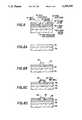
- FIG. 3shows a GaAs MES-FET fabricated by a method of a first preferred embodiment according to the invention.
- the GaAs MES-FETincludes a semi-insulation GaAs substrate 30, an n-GaAs function layer 32, an n-GaAs layer 34, an n + -GaAs layer 36, an ohmic electrode 38 and a gate electrode 40.
- the n-GaAs active layer 32is formed on the semi-insulation substrate 30 to have an impurity concentration of 2 ⁇ 10 17 cm -3 and a depth of 0.3 ⁇ m by MBE (molecular beam epitaxy) method, as shown in FIG. 4A.
- the n-GaAs active layer 32may be formed by ion implantation method using Is ion with implantation energy of 100 KeV and dose of 4 ⁇ 10 12 cm -2 .
- WSiTeungsten-silicide
- the gate electrode 40is sputtered on the n-GaAs active layer 32 to have a thickness of 3000 to 4000 ⁇ , and the WSi layer is shaped in vertical direction by reactive ion etching under the condition of mixed gas of CF 4 and CF 6 , pressure of 5 to 1 mToor and power of 150 to 600 W, using a photoresist having a thickness of 1 ⁇ m ("TSMR-8900" by "Tokyo Application Chemistry Corporation") as a mask.
- TSMR-8900photoresist having a thickness of 1 ⁇ m
- an insulation layersuch as of SiO 2 is dumped to have a thickness of 2000 ⁇ on the whole surface of the substrate thus processed.
- the thickness of the insulationshould be determined as precisely specified, because a distance between the gate electrode 40 and the edge of the recess is defined based on the thickness of the insulation layer. And, a first side wall 42 is then formed on the side surface of the gate electrode 40 by anisotropy dry etching, as shown in FIG. 4B.
- the n-GaAs layer 34is selectively grown by a vapor growth method such as MOCVD (Metal Organic CVD) method, as shown in FIG. 4C.
- MOCVDMetal Organic CVD
- This processis carried out under the condition that mixed gas of TMG (trimethylgallium) and AsH 3 (arsine) is used with Is 2 H 6 as dopant under the growth temperature of 500° to 600° C.
- a second side wall 44is formed on the surface of the gate electrode 40 covered with the first side wall 42.
- the n + -GaAs layer 36is formed on the n-GaAs layer 34 by vapor growth using the first and second side walls 42 and 44 as a mask, as shown in FIG. 4D.
- the n + -GaAs layer 36is to be a contact layer.
- the first and second side walls 42 and 44are removed by etching using hydrofluoric acid.
- ohmic metalis evaporated on the n + -GaAs layer 36 and alloyed whereby the ohmic electrode 38 is formed as shown in FIG. 3.
- two recesses 45 and 46are formed around the gate electrode 40 by self alignment.
- a distance between the gate electrode and each of the recess edgescan be controlled with high precision in accordance with the thickness of the side walls in the first preferred embodiment, so that the control property of a gate electrode break-down voltage is obtained with extremely high precision.
- the control property of a drain currentis not deteriorated at all.
- the fluctuation of a drain current flowing in a wafer of 3 inchesis approximately 10 mA in the GaAs MES-FET fabricated by the conventional method having the recess-etching step, while the drain current fluctuation is decreased as small as less than 4 mA in the GaAs MES-FET fabricated by the method in the first preferred embodiment.
- the fluctuation of more than 0.1 ⁇ mis observed in the conventionally fabricated GaAs MES-FET, while it is suppressed less than 0.02 ++m in the first preferred embodiment. Consequently, the fluctuation of a gate electrode break-down voltage can be negligible in the invention.
- FIG. 5shows a GaAs MES-FET fabricated by a method of a second preferred embodiment according to the invention.
- the GaAs MES-FETincludes a semi-insulation GaAs substrate 50, an n-GaAs active layer 52, an n-GaAs layer 54, an n + -GaAs layer 56, an ohmic electrode 58 and a gate electrode 60.
- the n-GaAs function layer 52is formed on the semi-insulation substrate 50 to have impurity concentration of 2 ⁇ 10 17 cm -3 and a depth of 0.3 ⁇ m by MBE (molecular beam epitaxy) method, as shown in FIG. 6A.
- the n-GaAs function layer 52may be formed by ion implantation method using Is ion with implantation energy of 100 KeV and dose of 4 ⁇ 10 12 cm -2 .
- WSiTeungsten-silicide
- the gate electrode 60is sputtered on the n-GaAs function layer 52 to have a thickness of 3000 to 4000 ⁇ , and the WSi layer is shaped in vertical direction by reactive ion etching using a photoresist layer (not shown) as a mask.
- the n-GaAs layer 54is selectively grown on the n-GaAs active layer 52 by a vapor growth method such as MOCVD (Metal Organic CVD) method using the gate electrode 60 as a mask, as shown in FIG. 6B.
- MOCVDMetal Organic CVD
- a insulation layer(not shown) is formed on the whole surface of the substrate thus processed, and a first side wall 62 is formed on the side surface of the gate electrode 60 by reactive dry etching, as shown in FIG. 6C.
- the n + -GaAs layer 56which will be a contact layer is formed on the n-GaAs layer 54 by vapor growth using the first side wall 52 as a mask, as shown in FIG. 6D.
- the first side wall 62is removed by etching, whereby a first recess 64 is formed around the gate electrode 60.
- ohmic metalis evaporated on the n + -GaAs layer 56 and is alloyed whereby the ohmic electrode 58 is formed as shown in FIG. 5. At this time, the ohmic metal is not evaporated around the gate electrode 60 whereby a second recess 64 is formed there.
- a surface condition around the gate electrode 60is stable, because the gate electrode 60 is buried at the bottom in the channel, that is, the n-GaAs layer 54.
- an undoped GaAs layer or an un-doped AlGaAs layermay be selectively grown on the n-GaAs operation layer 52 instead of the n-GaAs layer 54.
- the AlGaAs layeris grown by MOCVD (Metal Organic CVD) method in the condition that TMAl (trimethylaluminium) is added in mixed gas of TMG (trimethylgallium) and AsH 3 (arsine).
- MOCVDMetal Organic CVD
Landscapes
- Engineering & Computer Science (AREA)
- Physics & Mathematics (AREA)
- Condensed Matter Physics & Semiconductors (AREA)
- General Physics & Mathematics (AREA)
- Manufacturing & Machinery (AREA)
- Computer Hardware Design (AREA)
- Microelectronics & Electronic Packaging (AREA)
- Power Engineering (AREA)
- Chemical & Material Sciences (AREA)
- Materials Engineering (AREA)
- Junction Field-Effect Transistors (AREA)
Abstract
Description
Claims (2)
Applications Claiming Priority (2)
| Application Number | Priority Date | Filing Date | Title |
|---|---|---|---|
| JP4130918AJPH05326561A (en) | 1992-05-22 | 1992-05-22 | Method for manufacturing field effect transistor |
| JP4-130918 | 1992-05-22 |
Publications (1)
| Publication Number | Publication Date |
|---|---|
| US5298445Atrue US5298445A (en) | 1994-03-29 |
Family
ID=15045786
Family Applications (1)
| Application Number | Title | Priority Date | Filing Date |
|---|---|---|---|
| US08/065,622Expired - LifetimeUS5298445A (en) | 1992-05-22 | 1993-05-21 | Method for fabricating a field effect transistor |
Country Status (2)
| Country | Link |
|---|---|
| US (1) | US5298445A (en) |
| JP (1) | JPH05326561A (en) |
Cited By (29)
| Publication number | Priority date | Publication date | Assignee | Title |
|---|---|---|---|---|
| US5591666A (en)* | 1995-08-07 | 1997-01-07 | Motorola | Semiconductor device and method of fabrication |
| US5759880A (en)* | 1997-01-02 | 1998-06-02 | Motorola, Inc. | Resistless methods of fabricating FETs |
| US5879998A (en)* | 1997-07-09 | 1999-03-09 | Advanced Micro Devices, Inc. | Adaptively controlled, self-aligned, short channel device and method for manufacturing same |
| US20030102482A1 (en)* | 2001-12-03 | 2003-06-05 | Saxler Adam William | Strain balanced nitride heterojunction transistors and methods of fabricating strain balanced nitride heterojunction transistors |
| US6679997B2 (en)* | 1998-08-12 | 2004-01-20 | Nec Compound Semiconductor Devices, Ltd. | Organic insulation film formation method |
| US20040061129A1 (en)* | 2002-07-16 | 2004-04-01 | Saxler Adam William | Nitride-based transistors and methods of fabrication thereof using non-etched contact recesses |
| US20050170574A1 (en)* | 2004-01-16 | 2005-08-04 | Sheppard Scott T. | Nitride-based transistors with a protective layer and a low-damage recess and methods of fabrication thereof |
| US20050173728A1 (en)* | 2004-02-05 | 2005-08-11 | Saxler Adam W. | Nitride heterojunction transistors having charge-transfer induced energy barriers and methods of fabricating the same |
| US20050258450A1 (en)* | 2004-05-20 | 2005-11-24 | Saxler Adam W | Semiconductor devices having a hybrid channel layer, current aperture transistors and methods of fabricating same |
| US20050258451A1 (en)* | 2004-05-20 | 2005-11-24 | Saxler Adam W | Methods of fabricating nitride-based transistors having regrown ohmic contact regions and nitride-based transistors having regrown ohmic contact regions |
| US20060017064A1 (en)* | 2004-07-26 | 2006-01-26 | Saxler Adam W | Nitride-based transistors having laterally grown active region and methods of fabricating same |
| US20060019435A1 (en)* | 2004-07-23 | 2006-01-26 | Scott Sheppard | Methods of fabricating nitride-based transistors with a cap layer and a recessed gate |
| US20060108606A1 (en)* | 2004-11-23 | 2006-05-25 | Saxler Adam W | Cap layers and/or passivation layers for nitride-based transistors, transistor structures and methods of fabricating same |
| US20060118809A1 (en)* | 2004-12-06 | 2006-06-08 | Primit Parikh | High power density and/or linearity transistors |
| US20060118823A1 (en)* | 2004-12-06 | 2006-06-08 | Primit Parikh | Field effect transistors (FETs) having multi-watt output power at millimeter-wave frequencies |
| US20060208280A1 (en)* | 2005-03-15 | 2006-09-21 | Smith Richard P | Group III nitride field effect transistors (FETS) capable of withstanding high temperature reverse bias test conditions |
| US20060226412A1 (en)* | 2005-04-11 | 2006-10-12 | Saxler Adam W | Thick semi-insulating or insulating epitaxial gallium nitride layers and devices incorporating same |
| US20060226413A1 (en)* | 2005-04-11 | 2006-10-12 | Saxler Adam W | Composite substrates of conductive and insulating or semi-insulating group III-nitrides for group III-nitride devices |
| US20060244010A1 (en)* | 2005-04-29 | 2006-11-02 | Saxler Adam W | Aluminum free group III-nitride based high electron mobility transistors and methods of fabricating same |
| US20060244011A1 (en)* | 2005-04-29 | 2006-11-02 | Saxler Adam W | Binary group III-nitride based high electron mobility transistors and methods of fabricating same |
| US20060255364A1 (en)* | 2004-02-05 | 2006-11-16 | Saxler Adam W | Heterojunction transistors including energy barriers and related methods |
| US20070004184A1 (en)* | 2005-06-29 | 2007-01-04 | Saxler Adam W | Low dislocation density group III nitride layers on silicon carbide substrates and methods of making the same |
| US20070018198A1 (en)* | 2005-07-20 | 2007-01-25 | Brandes George R | High electron mobility electronic device structures comprising native substrates and methods for making the same |
| US20070164322A1 (en)* | 2006-01-17 | 2007-07-19 | Cree, Inc. | Methods of fabricating transistors including dielectrically-supported gate electrodes and related devices |
| US20070164315A1 (en)* | 2004-11-23 | 2007-07-19 | Cree, Inc. | Cap Layers Including Aluminum Nitride for Nitride-Based Transistors and Methods of Fabricating Same |
| DE102006022507A1 (en)* | 2006-05-15 | 2007-11-22 | United Monolithic Semiconductors Gmbh | A method of manufacturing a semiconductor device having a metallic gate electrode arranged in a double trench structure |
| US20090224289A1 (en)* | 2006-01-17 | 2009-09-10 | Cree, Inc. | Transistors including supported gate electrodes |
| US20100068855A1 (en)* | 2004-01-16 | 2010-03-18 | Cree, Inc. | Group III nitride semiconductor devices with silicon nitride layers and methods of manufacturing such devices |
| US8823057B2 (en) | 2006-11-06 | 2014-09-02 | Cree, Inc. | Semiconductor devices including implanted regions for providing low-resistance contact to buried layers and related devices |
Citations (11)
| Publication number | Priority date | Publication date | Assignee | Title |
|---|---|---|---|---|
| JPS61161770A (en)* | 1985-01-11 | 1986-07-22 | Nec Corp | Manufacture of semiconductor device |
| US4632710A (en)* | 1983-05-10 | 1986-12-30 | Raytheon Company | Vapor phase epitaxial growth of carbon doped layers of Group III-V materials |
| US4711858A (en)* | 1985-07-12 | 1987-12-08 | International Business Machines Corporation | Method of fabricating a self-aligned metal-semiconductor FET having an insulator spacer |
| JPS63281473A (en)* | 1987-05-13 | 1988-11-17 | Nec Corp | Field-effect semiconductor device and manufacture thereof |
| JPH02105425A (en)* | 1988-10-14 | 1990-04-18 | Nec Corp | Manufacture of semiconductor device |
| JPH02113539A (en)* | 1988-10-21 | 1990-04-25 | Nec Corp | Manufacture of semiconductor device |
| JPH02150038A (en)* | 1988-11-30 | 1990-06-08 | Sharp Corp | Modulation doped field effect transistor |
| US4977100A (en)* | 1988-10-12 | 1990-12-11 | Mitsubishi Denki Kabushiki Kaisha | Method of fabricating a MESFET |
| GB2252873A (en)* | 1991-02-14 | 1992-08-19 | Mitsubishi Electric Corp | Method of fabricating a field effect transistor |
| US5182218A (en)* | 1991-02-25 | 1993-01-26 | Sumitomo Electric Industries, Ltd. | Production methods for compound semiconductor device having lightly doped drain structure |
| US5196359A (en)* | 1988-06-30 | 1993-03-23 | Texas Instruments Incorporated | Method of forming heterostructure field effect transistor |
Family Cites Families (1)
| Publication number | Priority date | Publication date | Assignee | Title |
|---|---|---|---|---|
| JPH05218098A (en)* | 1992-02-06 | 1993-08-27 | Toshiba Corp | Heterojunction field-effect transistor and its manufacture |
- 1992
- 1992-05-22JPJP4130918Apatent/JPH05326561A/enactivePending
- 1993
- 1993-05-21USUS08/065,622patent/US5298445A/ennot_activeExpired - Lifetime
Patent Citations (11)
| Publication number | Priority date | Publication date | Assignee | Title |
|---|---|---|---|---|
| US4632710A (en)* | 1983-05-10 | 1986-12-30 | Raytheon Company | Vapor phase epitaxial growth of carbon doped layers of Group III-V materials |
| JPS61161770A (en)* | 1985-01-11 | 1986-07-22 | Nec Corp | Manufacture of semiconductor device |
| US4711858A (en)* | 1985-07-12 | 1987-12-08 | International Business Machines Corporation | Method of fabricating a self-aligned metal-semiconductor FET having an insulator spacer |
| JPS63281473A (en)* | 1987-05-13 | 1988-11-17 | Nec Corp | Field-effect semiconductor device and manufacture thereof |
| US5196359A (en)* | 1988-06-30 | 1993-03-23 | Texas Instruments Incorporated | Method of forming heterostructure field effect transistor |
| US4977100A (en)* | 1988-10-12 | 1990-12-11 | Mitsubishi Denki Kabushiki Kaisha | Method of fabricating a MESFET |
| JPH02105425A (en)* | 1988-10-14 | 1990-04-18 | Nec Corp | Manufacture of semiconductor device |
| JPH02113539A (en)* | 1988-10-21 | 1990-04-25 | Nec Corp | Manufacture of semiconductor device |
| JPH02150038A (en)* | 1988-11-30 | 1990-06-08 | Sharp Corp | Modulation doped field effect transistor |
| GB2252873A (en)* | 1991-02-14 | 1992-08-19 | Mitsubishi Electric Corp | Method of fabricating a field effect transistor |
| US5182218A (en)* | 1991-02-25 | 1993-01-26 | Sumitomo Electric Industries, Ltd. | Production methods for compound semiconductor device having lightly doped drain structure |
Non-Patent Citations (4)
| Title |
|---|
| Macksey, "GaAs Power FET's Having the Gate recess Narrower than the Gate", IEEE Electron Letter, vol. EDL 7, No. 2, Feb. 1986, pp. 69-70. |
| Macksey, GaAs Power FET s Having the Gate recess Narrower than the Gate , IEEE Electron Letter, vol. EDL 7, No. 2, Feb. 1986, pp. 69 70.* |
| Sonoda et al; "High-Efficiency and Highly Reliable 20W GaAs Power Field Effect Transistor in C Band"; Jpn. J. Appl. Phys. vol. 31 (8) part 1, Aug. 1992, pp. 2374-2381. |
| Sonoda et al; High Efficiency and Highly Reliable 20W GaAs Power Field Effect Transistor in C Band ; Jpn. J. Appl. Phys. vol. 31 (8) part 1, Aug. 1992, pp. 2374 2381.* |
Cited By (78)
| Publication number | Priority date | Publication date | Assignee | Title |
|---|---|---|---|---|
| US5591666A (en)* | 1995-08-07 | 1997-01-07 | Motorola | Semiconductor device and method of fabrication |
| US5759880A (en)* | 1997-01-02 | 1998-06-02 | Motorola, Inc. | Resistless methods of fabricating FETs |
| US5879998A (en)* | 1997-07-09 | 1999-03-09 | Advanced Micro Devices, Inc. | Adaptively controlled, self-aligned, short channel device and method for manufacturing same |
| US6679997B2 (en)* | 1998-08-12 | 2004-01-20 | Nec Compound Semiconductor Devices, Ltd. | Organic insulation film formation method |
| US7030428B2 (en) | 2001-12-03 | 2006-04-18 | Cree, Inc. | Strain balanced nitride heterojunction transistors |
| US20030102482A1 (en)* | 2001-12-03 | 2003-06-05 | Saxler Adam William | Strain balanced nitride heterojunction transistors and methods of fabricating strain balanced nitride heterojunction transistors |
| US8153515B2 (en) | 2001-12-03 | 2012-04-10 | Cree, Inc. | Methods of fabricating strain balanced nitride heterojunction transistors |
| US20060121682A1 (en)* | 2001-12-03 | 2006-06-08 | Cree, Inc. | Strain balanced nitride heterojunction transistors and methods of fabricating strain balanced nitride heterojunction transistors |
| US20040061129A1 (en)* | 2002-07-16 | 2004-04-01 | Saxler Adam William | Nitride-based transistors and methods of fabrication thereof using non-etched contact recesses |
| US7550784B2 (en) | 2002-07-16 | 2009-06-23 | Cree, Inc. | Nitride-based transistors and methods of fabrication thereof using non-etched contact recesses |
| WO2004008495A3 (en)* | 2002-07-16 | 2004-04-01 | Cree Inc | Nitride-based transistors and methods of fabrication thereof using non-etched contact recesses |
| US6982204B2 (en) | 2002-07-16 | 2006-01-03 | Cree, Inc. | Nitride-based transistors and methods of fabrication thereof using non-etched contact recesses |
| US20060006435A1 (en)* | 2002-07-16 | 2006-01-12 | Saxler Adam W | Nitride-based transistors and methods of fabrication thereof using non-etched contact recesses |
| US20100068855A1 (en)* | 2004-01-16 | 2010-03-18 | Cree, Inc. | Group III nitride semiconductor devices with silicon nitride layers and methods of manufacturing such devices |
| US20110136305A1 (en)* | 2004-01-16 | 2011-06-09 | Adam William Saxler | Group III Nitride Semiconductor Devices with Silicon Nitride Layers and Methods of Manufacturing Such Devices |
| US7906799B2 (en) | 2004-01-16 | 2011-03-15 | Cree, Inc. | Nitride-based transistors with a protective layer and a low-damage recess |
| US7045404B2 (en) | 2004-01-16 | 2006-05-16 | Cree, Inc. | Nitride-based transistors with a protective layer and a low-damage recess and methods of fabrication thereof |
| US20110140123A1 (en)* | 2004-01-16 | 2011-06-16 | Sheppard Scott T | Nitride-Based Transistors With a Protective Layer and a Low-Damage Recess |
| US20050170574A1 (en)* | 2004-01-16 | 2005-08-04 | Sheppard Scott T. | Nitride-based transistors with a protective layer and a low-damage recess and methods of fabrication thereof |
| US7901994B2 (en) | 2004-01-16 | 2011-03-08 | Cree, Inc. | Methods of manufacturing group III nitride semiconductor devices with silicon nitride layers |
| US11316028B2 (en) | 2004-01-16 | 2022-04-26 | Wolfspeed, Inc. | Nitride-based transistors with a protective layer and a low-damage recess |
| US8481376B2 (en) | 2004-01-16 | 2013-07-09 | Cree, Inc. | Group III nitride semiconductor devices with silicon nitride layers and methods of manufacturing such devices |
| US20060255366A1 (en)* | 2004-01-16 | 2006-11-16 | Sheppard Scott T | Nitride-based transistors with a protective layer and a low-damage recess |
| US9035354B2 (en) | 2004-02-05 | 2015-05-19 | Cree, Inc. | Heterojunction transistors having barrier layer bandgaps greater than channel layer bandgaps and related methods |
| US7612390B2 (en) | 2004-02-05 | 2009-11-03 | Cree, Inc. | Heterojunction transistors including energy barriers |
| US20050173728A1 (en)* | 2004-02-05 | 2005-08-11 | Saxler Adam W. | Nitride heterojunction transistors having charge-transfer induced energy barriers and methods of fabricating the same |
| US20060255364A1 (en)* | 2004-02-05 | 2006-11-16 | Saxler Adam W | Heterojunction transistors including energy barriers and related methods |
| US7170111B2 (en) | 2004-02-05 | 2007-01-30 | Cree, Inc. | Nitride heterojunction transistors having charge-transfer induced energy barriers and methods of fabricating the same |
| US20100187570A1 (en)* | 2004-02-05 | 2010-07-29 | Adam William Saxler | Heterojunction Transistors Having Barrier Layer Bandgaps Greater Than Channel Layer Bandgaps and Related Methods |
| US20050258451A1 (en)* | 2004-05-20 | 2005-11-24 | Saxler Adam W | Methods of fabricating nitride-based transistors having regrown ohmic contact regions and nitride-based transistors having regrown ohmic contact regions |
| US20050258450A1 (en)* | 2004-05-20 | 2005-11-24 | Saxler Adam W | Semiconductor devices having a hybrid channel layer, current aperture transistors and methods of fabricating same |
| US7084441B2 (en) | 2004-05-20 | 2006-08-01 | Cree, Inc. | Semiconductor devices having a hybrid channel layer, current aperture transistors and methods of fabricating same |
| US7479669B2 (en) | 2004-05-20 | 2009-01-20 | Cree, Inc. | Current aperture transistors and methods of fabricating same |
| US7432142B2 (en) | 2004-05-20 | 2008-10-07 | Cree, Inc. | Methods of fabricating nitride-based transistors having regrown ohmic contact regions |
| US20070254418A1 (en)* | 2004-07-23 | 2007-11-01 | Scott Sheppard | Methods of fabricating nitride-based transistors with a cap layer and a recessed gate |
| US20100140664A1 (en)* | 2004-07-23 | 2010-06-10 | Scott Sheppard | Methods of Fabricating Nitride-Based Transistors with a Cap Layer and a Recessed Gate and Related Devices |
| US7678628B2 (en) | 2004-07-23 | 2010-03-16 | Cree, Inc. | Methods of fabricating nitride-based transistors with a cap layer and a recessed gate |
| US9666707B2 (en) | 2004-07-23 | 2017-05-30 | Cree, Inc. | Nitride-based transistors with a cap layer and a recessed gate |
| US7238560B2 (en) | 2004-07-23 | 2007-07-03 | Cree, Inc. | Methods of fabricating nitride-based transistors with a cap layer and a recessed gate |
| US20060019435A1 (en)* | 2004-07-23 | 2006-01-26 | Scott Sheppard | Methods of fabricating nitride-based transistors with a cap layer and a recessed gate |
| US20060017064A1 (en)* | 2004-07-26 | 2006-01-26 | Saxler Adam W | Nitride-based transistors having laterally grown active region and methods of fabricating same |
| US20100012952A1 (en)* | 2004-07-26 | 2010-01-21 | Adam William Saxler | Nitride-Based Transistors Having Laterally Grown Active Region and Methods of Fabricating Same |
| US8946777B2 (en) | 2004-07-26 | 2015-02-03 | Cree, Inc. | Nitride-based transistors having laterally grown active region and methods of fabricating same |
| US7456443B2 (en) | 2004-11-23 | 2008-11-25 | Cree, Inc. | Transistors having buried n-type and p-type regions beneath the source region |
| US20070164315A1 (en)* | 2004-11-23 | 2007-07-19 | Cree, Inc. | Cap Layers Including Aluminum Nitride for Nitride-Based Transistors and Methods of Fabricating Same |
| US20060108606A1 (en)* | 2004-11-23 | 2006-05-25 | Saxler Adam W | Cap layers and/or passivation layers for nitride-based transistors, transistor structures and methods of fabricating same |
| US20090042345A1 (en)* | 2004-11-23 | 2009-02-12 | Cree, Inc. | Methods of Fabricating Transistors Having Buried N-Type and P-Type Regions Beneath the Source Region |
| US7709859B2 (en) | 2004-11-23 | 2010-05-04 | Cree, Inc. | Cap layers including aluminum nitride for nitride-based transistors |
| US9166033B2 (en) | 2004-11-23 | 2015-10-20 | Cree, Inc. | Methods of passivating surfaces of wide bandgap semiconductor devices |
| US20060118809A1 (en)* | 2004-12-06 | 2006-06-08 | Primit Parikh | High power density and/or linearity transistors |
| US7355215B2 (en) | 2004-12-06 | 2008-04-08 | Cree, Inc. | Field effect transistors (FETs) having multi-watt output power at millimeter-wave frequencies |
| US20060118823A1 (en)* | 2004-12-06 | 2006-06-08 | Primit Parikh | Field effect transistors (FETs) having multi-watt output power at millimeter-wave frequencies |
| US7161194B2 (en) | 2004-12-06 | 2007-01-09 | Cree, Inc. | High power density and/or linearity transistors |
| US20060208280A1 (en)* | 2005-03-15 | 2006-09-21 | Smith Richard P | Group III nitride field effect transistors (FETS) capable of withstanding high temperature reverse bias test conditions |
| US8803198B2 (en) | 2005-03-15 | 2014-08-12 | Cree, Inc. | Group III nitride field effect transistors (FETS) capable of withstanding high temperature reverse bias test conditions |
| US8212289B2 (en) | 2005-03-15 | 2012-07-03 | Cree, Inc. | Group III nitride field effect transistors (FETS) capable of withstanding high temperature reverse bias test conditions |
| US7465967B2 (en) | 2005-03-15 | 2008-12-16 | Cree, Inc. | Group III nitride field effect transistors (FETS) capable of withstanding high temperature reverse bias test conditions |
| US20060226413A1 (en)* | 2005-04-11 | 2006-10-12 | Saxler Adam W | Composite substrates of conductive and insulating or semi-insulating group III-nitrides for group III-nitride devices |
| US9224596B2 (en) | 2005-04-11 | 2015-12-29 | Cree, Inc. | Methods of fabricating thick semi-insulating or insulating epitaxial gallium nitride layers |
| US20060226412A1 (en)* | 2005-04-11 | 2006-10-12 | Saxler Adam W | Thick semi-insulating or insulating epitaxial gallium nitride layers and devices incorporating same |
| US8575651B2 (en) | 2005-04-11 | 2013-11-05 | Cree, Inc. | Devices having thick semi-insulating epitaxial gallium nitride layer |
| US7626217B2 (en) | 2005-04-11 | 2009-12-01 | Cree, Inc. | Composite substrates of conductive and insulating or semi-insulating group III-nitrides for group III-nitride devices |
| US20060244010A1 (en)* | 2005-04-29 | 2006-11-02 | Saxler Adam W | Aluminum free group III-nitride based high electron mobility transistors and methods of fabricating same |
| US7615774B2 (en) | 2005-04-29 | 2009-11-10 | Cree.Inc. | Aluminum free group III-nitride based high electron mobility transistors |
| US7544963B2 (en) | 2005-04-29 | 2009-06-09 | Cree, Inc. | Binary group III-nitride based high electron mobility transistors |
| US20060244011A1 (en)* | 2005-04-29 | 2006-11-02 | Saxler Adam W | Binary group III-nitride based high electron mobility transistors and methods of fabricating same |
| US9331192B2 (en) | 2005-06-29 | 2016-05-03 | Cree, Inc. | Low dislocation density group III nitride layers on silicon carbide substrates and methods of making the same |
| US20070004184A1 (en)* | 2005-06-29 | 2007-01-04 | Saxler Adam W | Low dislocation density group III nitride layers on silicon carbide substrates and methods of making the same |
| US20070018198A1 (en)* | 2005-07-20 | 2007-01-25 | Brandes George R | High electron mobility electronic device structures comprising native substrates and methods for making the same |
| US8049252B2 (en) | 2006-01-17 | 2011-11-01 | Cree, Inc. | Methods of fabricating transistors including dielectrically-supported gate electrodes and related devices |
| US20090224289A1 (en)* | 2006-01-17 | 2009-09-10 | Cree, Inc. | Transistors including supported gate electrodes |
| US7709269B2 (en) | 2006-01-17 | 2010-05-04 | Cree, Inc. | Methods of fabricating transistors including dielectrically-supported gate electrodes |
| US7960756B2 (en) | 2006-01-17 | 2011-06-14 | Cree, Inc. | Transistors including supported gate electrodes |
| US7592211B2 (en) | 2006-01-17 | 2009-09-22 | Cree, Inc. | Methods of fabricating transistors including supported gate electrodes |
| US20070164322A1 (en)* | 2006-01-17 | 2007-07-19 | Cree, Inc. | Methods of fabricating transistors including dielectrically-supported gate electrodes and related devices |
| DE102006022507A1 (en)* | 2006-05-15 | 2007-11-22 | United Monolithic Semiconductors Gmbh | A method of manufacturing a semiconductor device having a metallic gate electrode arranged in a double trench structure |
| US8823057B2 (en) | 2006-11-06 | 2014-09-02 | Cree, Inc. | Semiconductor devices including implanted regions for providing low-resistance contact to buried layers and related devices |
| US9984881B2 (en) | 2006-11-06 | 2018-05-29 | Cree, Inc. | Methods of fabricating semiconductor devices including implanted regions for providing low-resistance contact to buried layers and related devices |
Also Published As
| Publication number | Publication date |
|---|---|
| JPH05326561A (en) | 1993-12-10 |
Similar Documents
| Publication | Publication Date | Title |
|---|---|---|
| US5298445A (en) | Method for fabricating a field effect transistor | |
| US5675159A (en) | Recessed gate field effect transistor | |
| CA1214575A (en) | Method of manufacturing gaas semiconductor device | |
| EP0592064B1 (en) | Method of producing a field effect transistor | |
| US5468343A (en) | Etching solution and etching method for semiconductors and method for evaluating GaAs surface | |
| US5399896A (en) | FET with a T-shaped gate of a particular structure | |
| US20010015437A1 (en) | GaN field-effect transistor, inverter device, and production processes therefor | |
| US4751195A (en) | Method of manufacturing a heterojunction bipolar transistor | |
| US5886373A (en) | Field effect transistor | |
| EP0855748B1 (en) | Heterojunction field-effect transistor and method of fabricating the same | |
| US5170230A (en) | Semiconductor device and production method thereof | |
| EP0539688B1 (en) | Compound semiconductor device and production method therefor | |
| EP0461807B1 (en) | MESFET and manufacturing method therefor | |
| US5389574A (en) | Selective etching method for III-V group semiconductor material using a mixed etching gas and a stop-etching gas | |
| US5296389A (en) | Method of fabricating a heterojunction bipolar transistor | |
| EP0367411A2 (en) | Heterojunction semiconductor devices and methods of making the same | |
| EP0892441A2 (en) | Field effect transistor with recessed gate and a method for manufacturing the same | |
| US5837570A (en) | Heterostructure semiconductor device and method of fabricating same | |
| KR950007361B1 (en) | Field effect transistor | |
| JPH11177079A (en) | Field-effect transistor | |
| JP3109590B2 (en) | Method for manufacturing semiconductor device | |
| US5786610A (en) | Field effect transistor | |
| JP3143965B2 (en) | Method for manufacturing semiconductor device | |
| JPS59205765A (en) | Manufacture of semiconductor device | |
| US5698871A (en) | Heterojunction bipolar transistor |
Legal Events
| Date | Code | Title | Description |
|---|---|---|---|
| AS | Assignment | Owner name:NEC CORPORATION, JAPAN Free format text:ASSIGNMENT OF ASSIGNORS INTEREST;ASSIGNOR:ASANO, KAZUNORI;REEL/FRAME:006574/0084 Effective date:19930519 | |
| STPP | Information on status: patent application and granting procedure in general | Free format text:APPLICATION UNDERGOING PREEXAM PROCESSING | |
| FEPP | Fee payment procedure | Free format text:PAYOR NUMBER ASSIGNED (ORIGINAL EVENT CODE: ASPN); ENTITY STATUS OF PATENT OWNER: LARGE ENTITY | |
| FPAY | Fee payment | Year of fee payment:4 | |
| FEPP | Fee payment procedure | Free format text:PAYOR NUMBER ASSIGNED (ORIGINAL EVENT CODE: ASPN); ENTITY STATUS OF PATENT OWNER: LARGE ENTITY Free format text:PAYER NUMBER DE-ASSIGNED (ORIGINAL EVENT CODE: RMPN); ENTITY STATUS OF PATENT OWNER: LARGE ENTITY | |
| FPAY | Fee payment | Year of fee payment:8 | |
| AS | Assignment | Owner name:NEC COMPOUND SEMICONDUCTOR DEVICES, LTD., JAPAN Free format text:ASSIGNMENT OF ASSIGNORS INTEREST;ASSIGNOR:NEC CORPORATION;REEL/FRAME:014669/0477 Effective date:20020919 | |
| FPAY | Fee payment | Year of fee payment:12 | |
| AS | Assignment | Owner name:NEC ELECTRONICS CORPORATION, JAPAN Free format text:ASSIGNMENT OF ASSIGNORS INTEREST;ASSIGNOR:NEC COMPOUND SEMICONDUCTOR DEVICES, LTD.;REEL/FRAME:017422/0528 Effective date:20060315 |