US5297271A - Method and apparatus for performing a read-write-modify operation in a VGA compatible controller - Google Patents
Method and apparatus for performing a read-write-modify operation in a VGA compatible controllerDownload PDFInfo
- Publication number
- US5297271A US5297271AUS08/052,238US5223893AUS5297271AUS 5297271 AUS5297271 AUS 5297271AUS 5223893 AUS5223893 AUS 5223893AUS 5297271 AUS5297271 AUS 5297271A
- Authority
- US
- United States
- Prior art keywords
- read
- modify
- write
- memory
- video graphics
- Prior art date
- Legal status (The legal status is an assumption and is not a legal conclusion. Google has not performed a legal analysis and makes no representation as to the accuracy of the status listed.)
- Expired - Lifetime
Links
Images


Classifications
- G—PHYSICS
- G09—EDUCATION; CRYPTOGRAPHY; DISPLAY; ADVERTISING; SEALS
- G09G—ARRANGEMENTS OR CIRCUITS FOR CONTROL OF INDICATING DEVICES USING STATIC MEANS TO PRESENT VARIABLE INFORMATION
- G09G5/00—Control arrangements or circuits for visual indicators common to cathode-ray tube indicators and other visual indicators
- G09G5/36—Control arrangements or circuits for visual indicators common to cathode-ray tube indicators and other visual indicators characterised by the display of a graphic pattern, e.g. using an all-points-addressable [APA] memory
- G09G5/39—Control of the bit-mapped memory
- G09G5/393—Arrangements for updating the contents of the bit-mapped memory
Definitions
- the present inventionrelates generally to computer graphics, and more specifically to improvements in a Video Graphics Array ( ⁇ VGA ⁇ ) controller.
- ⁇ VGA ⁇Video Graphics Array
- a typical prior art VGA controllerhas an associated display memory, which consists of an array of dynamic RAM (DRAM) chips.
- DRAMdynamic RAM
- each pixel on the displayhas a corresponding display memory location which contains a code (typically 4 or 8 bits) representing the color of that pixel.
- the CPUcontrols the display by writing data to the graphics controller.
- the graphics controllerresponds to such data by updating the relevant data entries in the display memory.
- Bit Block TransferOne of the most commonly executed functions in raster graphics applications is to move and/or modify the stored bit map of the raster image. This function is known as Bit Block Transfer, or BitBlt.
- Bit Block Transfer operationsthe rectangular bit map for the stored raster image is modified by performing logical operations upon it and a second, different, bit map of the raster image. These logical operations are called RasterOps.
- Steps (a) through (e)are repeated for all VGA memory addresses that are encompassed by the destination rectangular bit map. All read and write operations are performed in software by the System CPU.
- a known solution to this problemis a read-modify-write cycle, wherein data is read, modified and rewritten, all in one cycle. Although these cycles are known and have been in use even prior to the implementation of read-modify-write cycles in DRAM, no known VGA controller has implemented a read-modify-write cycle for use in raster graphics operations.
- the present inventionprovides a method and an apparatus within a VGA controller for implementing a read-modify-write cycle for use in raster graphics operations.
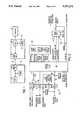
- FIG. 1is a high level block diagram of a computer system including a graphics board having a VGA controller chip;
- FIG. 2is a block diagram of the graphics board
- FIG. 3is a block diagram of the VGA controller chip
- FIG. 4is a block diagram of the graphics controller portion of the VGA controller chip.
- FIG. 5is a block diagram of the present invention when the read-modify-write cycle is being used.
- FIG. 1is high level block diagram of a computer system including a processor subsystem 10, a graphics subsystem 12, and a display 13.
- the computer subsystemincludes a CPU 15, an associated memory 17, and an expansion bus interface 18 to an expansion bus 20.
- graphics subsystem 12is typically implemented on a circuit board that plugs into a connector on expansion bus 20, it will be referred to as graphics board 12.
- the graphics boardis coupled to the expansion bus by a bus interface 22, and further includes a controller unit 25 and an associated display memory 30.
- Bus 20may be an industry standard architecture (ISA) bus (sometimes called an AT-bus) or a Microchannel Architecture (MCA) bus.
- Controller unit 25is an extended VGA controller chip.
- FIG. 2is a block diagram of graphics board 12.
- Display memory 30is implemented as a video RAM (VRAM) array 30 that interfaces with VGA chip 25 through parallel and serial data ports.
- the graphics boardalso includes a BIOS ROM 32 and an optional color palette chip 40.
- the bus interfaceincludes buffers 35, a multiplexer 37, and a PAL chip 38.
- the general configuration of the graphics boardis known in the art, and will not be described further.
- FIG. 3is a block diagram of VGA chip 25 and VRAM array 30.
- the major functional entities of VGA chip 25include a graphics controller 50, an address multiplexer 55, a sequencer 60, an address generator 65, a CRT controller 70, and a video controller 75.
- Internal data and control buses 77 and 78couple the external data and control buses to the various functional entities.
- the display memoryconsists of an array of VRAM chips logically organized in four planes, each of which typically contains one or two VRAM chips. Planes 0, 1, 2, and 3 are shown with reference numerals 30a, 30b, 30c and 30d. When the VGA chip is in text mode, planes 0 and 1 contain text and attribute information, plane 2 contains font information and plane 3 is not used. When the VGA chip is in the graphics mode, all planes are merely parts of a bit-mapped display memory with 4 or 8 bits per pixel.
- Address multiplexer 55converts incoming address information to address signals that are communicated to display memory 30.
- both the memory buseshave the same value.
- Sequencer 60generates memory read, write or read-modify-write timing for CPU accesses, the DRAM refresh timing, and the data transfer cycle timing (which is specific to video RAMs) and arbitrates CPU read and write cycles, refresh cycles and data transfer cycles. It generates the row and column address strobes (RAS and CAS) and the Write Enable (WE), Output Enable (OE), and Shift Clock (SCLK) signals for the VRAMS.
- RAS and CASrow and column address strobes
- WEWrite Enable
- OEOutput Enable
- SCLKShift Clock
- Address generator 65generates linear addresses for VRAM refresh and communicates these to sequencer 60, which generates the actual addressing strobes.
- the address generatoris also responsible for video refresh and generates addresses to the display memory.
- CRT controller 70generates CRT timing for the monitor, namely the horizonal and vertical sync signals (HSYNC and VSYNC) and the blanking signal. It also provides timing control to the address generator for the video refresh and generates timing for sequencer to tell it when to access the VRAM array for video refresh.
- Video controller 75receives video information for the display, serializes it, and sends it out on the video bus. In the planar graphics mode, it sends a 6-bit color code from an internal color palette and two programmable bits onto the video bus. In the packed pixel mode it sends all 8 bits from the VRAM onto the video bus.
- FIG. 4is a block diagram of the graphics controller portion of VGA chip 25.
- This portion of the chipincludes write operation logic 80 and associated write operation control registers 82, read operation logic 85 and associated read operation control registers 87, and a set of CPU latches 90a-d.
- the CPU latcheshave inputs coupled to the data paths between the write operation logic and the display memory and are loaded from the display memory by a CPU read operation.
- the latch outputscommunicate with portions of the write operation logic and with the read operation logic.
- Write operation logic 80is shown as having four data paths, corresponding to the four memory planes.
- the data pathsinclude respective ALUs 95a-d for performing logical operations between incoming bus data, as possibly modified by input logic 97a-d, and the content of CPU latches 90a-d.
- the ALU outputsare communicated to the display memory.
- FIG. 5One embodiment of the present invention is shown in FIG. 5.
- the function of a read-modify-write operationis realized exclusively in hardware. Only one address source is used.
- the cycleproceeds in the following manner:
- the data operandis fetched from systems or VGA memory, stored in loqic 97a-d, and presented to VGA graphics controller 50.
- datais read from the VGA memory's write address, shown here as Address Multiplexer 55, and latched successively into VRAM 30a-d and CPU latch 90a-d.
- the desired logical operationis then performed on the operands using VGA graphics controller 50.
- the logical operationis performed on operands from the CPU write data and the VGA data specified in the VGA memory write address.
- the advantages of the present inventioninclude reducing the CPU read and write operation from two complete cycles requiring roughly 875 nanoseconds to one CPU write operation requiring between 500 to 625 nanoseconds. In many systems the read and write operations are even slower, increasing the speed advantage of the present invention. Additionally, as the present invention's data path has only one address source, the data that is read is always the data modified. The second operand always comes with the CPU write cycle. Finally, no software is required to perform the read cycle to obtain the destination data operand.
Landscapes
- Engineering & Computer Science (AREA)
- Physics & Mathematics (AREA)
- Computer Hardware Design (AREA)
- General Physics & Mathematics (AREA)
- Theoretical Computer Science (AREA)
- Controls And Circuits For Display Device (AREA)
Abstract
Description
Claims (5)
Priority Applications (1)
| Application Number | Priority Date | Filing Date | Title |
|---|---|---|---|
| US08/052,238US5297271A (en) | 1990-09-21 | 1993-04-21 | Method and apparatus for performing a read-write-modify operation in a VGA compatible controller |
Applications Claiming Priority (2)
| Application Number | Priority Date | Filing Date | Title |
|---|---|---|---|
| US58606090A | 1990-09-21 | 1990-09-21 | |
| US08/052,238US5297271A (en) | 1990-09-21 | 1993-04-21 | Method and apparatus for performing a read-write-modify operation in a VGA compatible controller |
Related Parent Applications (1)
| Application Number | Title | Priority Date | Filing Date |
|---|---|---|---|
| US58606090AContinuation | 1990-09-21 | 1990-09-21 |
Publications (1)
| Publication Number | Publication Date |
|---|---|
| US5297271Atrue US5297271A (en) | 1994-03-22 |
Family
ID=24344141
Family Applications (1)
| Application Number | Title | Priority Date | Filing Date |
|---|---|---|---|
| US08/052,238Expired - LifetimeUS5297271A (en) | 1990-09-21 | 1993-04-21 | Method and apparatus for performing a read-write-modify operation in a VGA compatible controller |
Country Status (1)
| Country | Link |
|---|---|
| US (1) | US5297271A (en) |
Cited By (11)
| Publication number | Priority date | Publication date | Assignee | Title |
|---|---|---|---|---|
| US5557733A (en)* | 1993-04-02 | 1996-09-17 | Vlsi Technology, Inc. | Caching FIFO and method therefor |
| US5640502A (en)* | 1994-08-05 | 1997-06-17 | Thomson Consumer Electronics, Inc. | Bit-mapped on-screen-display device for a television receiver |
| US5787240A (en)* | 1994-05-20 | 1998-07-28 | Fujitsu Ltd. | Printer control apparatus converting video data from an external host to video data for a printer |
| US5829007A (en) | 1993-06-24 | 1998-10-27 | Discovision Associates | Technique for implementing a swing buffer in a memory array |
| US5920714A (en)* | 1991-02-14 | 1999-07-06 | Cray Research, Inc. | System and method for distributed multiprocessor communications |
| US6018354A (en) | 1994-03-24 | 2000-01-25 | Discovision Associates | Method for accessing banks of DRAM |
| US6122315A (en)* | 1997-02-26 | 2000-09-19 | Discovision Associates | Memory manager for MPEG decoder |
| US7458005B1 (en)* | 2002-08-09 | 2008-11-25 | Virage Logic Corp. | System and method for providing adjustable read margins in a semiconductor memory |
| US20090223872A1 (en)* | 2008-03-07 | 2009-09-10 | Ronald Robbins | System and method for sorting items |
| WO2011022114A1 (en) | 2009-08-20 | 2011-02-24 | Rambus Inc. | Atomic memory device |
| US10083115B2 (en)* | 2016-04-19 | 2018-09-25 | SK Hynix Inc. | Memory controller and data storage apparatus including the same |
Citations (8)
| Publication number | Priority date | Publication date | Assignee | Title |
|---|---|---|---|---|
| US4639866A (en)* | 1984-01-24 | 1987-01-27 | International Computers Limited | Pipelined data processing apparatus |
| US4695967A (en)* | 1984-03-09 | 1987-09-22 | Daikin Industries, Ltd. | High speed memory access circuit of CRT display unit |
| US4941107A (en)* | 1986-11-17 | 1990-07-10 | Kabushiki Kaisha Toshiba | Image data processing apparatus |
| US5043918A (en)* | 1989-11-09 | 1991-08-27 | Dataproducts Corporation | Multiple bus image controller structure for color page printers |
| US5109520A (en)* | 1985-02-19 | 1992-04-28 | Tektronix, Inc. | Image frame buffer access speedup by providing multiple buffer controllers each containing command FIFO buffers |
| USRE33922E (en)* | 1984-10-05 | 1992-05-12 | Hitachi, Ltd. | Memory circuit for graphic images |
| US5115510A (en)* | 1987-10-20 | 1992-05-19 | Sharp Kabushiki Kaisha | Multistage data flow processor with instruction packet, fetch, storage transmission and address generation controlled by destination information |
| US5175838A (en)* | 1984-10-05 | 1992-12-29 | Hitachi, Ltd. | Memory circuit formed on integrated circuit device and having programmable function |
- 1993
- 1993-04-21USUS08/052,238patent/US5297271A/ennot_activeExpired - Lifetime
Patent Citations (8)
| Publication number | Priority date | Publication date | Assignee | Title |
|---|---|---|---|---|
| US4639866A (en)* | 1984-01-24 | 1987-01-27 | International Computers Limited | Pipelined data processing apparatus |
| US4695967A (en)* | 1984-03-09 | 1987-09-22 | Daikin Industries, Ltd. | High speed memory access circuit of CRT display unit |
| USRE33922E (en)* | 1984-10-05 | 1992-05-12 | Hitachi, Ltd. | Memory circuit for graphic images |
| US5175838A (en)* | 1984-10-05 | 1992-12-29 | Hitachi, Ltd. | Memory circuit formed on integrated circuit device and having programmable function |
| US5109520A (en)* | 1985-02-19 | 1992-04-28 | Tektronix, Inc. | Image frame buffer access speedup by providing multiple buffer controllers each containing command FIFO buffers |
| US4941107A (en)* | 1986-11-17 | 1990-07-10 | Kabushiki Kaisha Toshiba | Image data processing apparatus |
| US5115510A (en)* | 1987-10-20 | 1992-05-19 | Sharp Kabushiki Kaisha | Multistage data flow processor with instruction packet, fetch, storage transmission and address generation controlled by destination information |
| US5043918A (en)* | 1989-11-09 | 1991-08-27 | Dataproducts Corporation | Multiple bus image controller structure for color page printers |
Cited By (25)
| Publication number | Priority date | Publication date | Assignee | Title |
|---|---|---|---|---|
| US5920714A (en)* | 1991-02-14 | 1999-07-06 | Cray Research, Inc. | System and method for distributed multiprocessor communications |
| US5557733A (en)* | 1993-04-02 | 1996-09-17 | Vlsi Technology, Inc. | Caching FIFO and method therefor |
| US5829007A (en) | 1993-06-24 | 1998-10-27 | Discovision Associates | Technique for implementing a swing buffer in a memory array |
| US5835792A (en) | 1993-06-24 | 1998-11-10 | Discovision Associates | Token-based adaptive video processing arrangement |
| US6018354A (en) | 1994-03-24 | 2000-01-25 | Discovision Associates | Method for accessing banks of DRAM |
| US5787240A (en)* | 1994-05-20 | 1998-07-28 | Fujitsu Ltd. | Printer control apparatus converting video data from an external host to video data for a printer |
| US5984512A (en) | 1994-07-29 | 1999-11-16 | Discovision Associates | Method for storing video information |
| US5640502A (en)* | 1994-08-05 | 1997-06-17 | Thomson Consumer Electronics, Inc. | Bit-mapped on-screen-display device for a television receiver |
| US6122315A (en)* | 1997-02-26 | 2000-09-19 | Discovision Associates | Memory manager for MPEG decoder |
| US7458005B1 (en)* | 2002-08-09 | 2008-11-25 | Virage Logic Corp. | System and method for providing adjustable read margins in a semiconductor memory |
| US9827598B2 (en) | 2008-03-07 | 2017-11-28 | Engineering Innovation, Inc. | System and method for sorting items |
| US20090223872A1 (en)* | 2008-03-07 | 2009-09-10 | Ronald Robbins | System and method for sorting items |
| US10751758B2 (en) | 2008-03-07 | 2020-08-25 | Engineering Innovation, Inc. | System and method for sorting items |
| US20120117317A1 (en)* | 2009-08-20 | 2012-05-10 | Rambus Inc. | Atomic memory device |
| US20150178187A1 (en)* | 2009-08-20 | 2015-06-25 | Rambus Inc. | Single command, multiple column-operation memory device |
| US9658953B2 (en)* | 2009-08-20 | 2017-05-23 | Rambus Inc. | Single command, multiple column-operation memory device |
| EP2467852A4 (en)* | 2009-08-20 | 2014-04-02 | Rambus Inc | ATOMIC MEMORY DEVICE |
| US9898400B2 (en) | 2009-08-20 | 2018-02-20 | Rambus Inc. | Single command, multiple column-operation memory device |
| US10552310B2 (en) | 2009-08-20 | 2020-02-04 | Rambus Inc. | Single command, multiple column-operation memory device |
| WO2011022114A1 (en) | 2009-08-20 | 2011-02-24 | Rambus Inc. | Atomic memory device |
| US11204863B2 (en) | 2009-08-20 | 2021-12-21 | Rambus Inc. | Memory component that performs data write from pre-programmed register |
| US11720485B2 (en) | 2009-08-20 | 2023-08-08 | Rambus Inc. | DRAM with command-differentiated storage of internally and externally sourced data |
| US11748252B2 (en) | 2009-08-20 | 2023-09-05 | Rambus Inc. | Data write from pre-programmed register |
| US12189523B2 (en) | 2009-08-20 | 2025-01-07 | Rambus Inc. | Command-differentiated storage of internally and externally sourced data |
| US10083115B2 (en)* | 2016-04-19 | 2018-09-25 | SK Hynix Inc. | Memory controller and data storage apparatus including the same |
Similar Documents
| Publication | Publication Date | Title |
|---|---|---|
| US6154824A (en) | Multifunctional access devices, systems and methods | |
| US5392391A (en) | High performance graphics applications controller | |
| US4104624A (en) | Microprocessor controlled CRT display system | |
| EP0197412B1 (en) | Variable access frame buffer memory | |
| US5696923A (en) | Graphics processor writing to shadow register at predetermined address simultaneously with writing to control register | |
| KR980010997A (en) | Graphics Accelerator and Memory Prefetch Method Using It | |
| US4823281A (en) | Color graphic processor for performing logical operations | |
| US5297271A (en) | Method and apparatus for performing a read-write-modify operation in a VGA compatible controller | |
| EP0182454B1 (en) | Video system controller with a row address override circuit | |
| US5737761A (en) | Memory control architecture for high-speed transfer operations | |
| US5477242A (en) | Display adapter for virtual VGA support in XGA native mode | |
| US4747042A (en) | Display control system | |
| US5559533A (en) | Virtual memory hardware cusor and method | |
| EP0487819B1 (en) | Video random access memory with fast, alligned clear and copy | |
| US5900887A (en) | Multiplexed wide interface to SGRAM on a graphics controller for complex-pattern fills without color and mask registers | |
| US5642138A (en) | Display control system using a different clock in the graphics mode from that in the text mode in accessing an image memory | |
| US5699498A (en) | Technique and apparatus for color expansion into a non-aligned 24 bit RGB color-space format | |
| US5649172A (en) | Color mixing device using a high speed image register | |
| JP3017882B2 (en) | Display control system | |
| JP2794481B2 (en) | Display system | |
| US5633661A (en) | Video display control system having block write with opaque pattern control expansion | |
| KR920003642Y1 (en) | Circuit for accelcrating the speed of graphic process | |
| JP3874781B2 (en) | Method for supplying image data to monitor and graphic memory control device | |
| JPH03144492A (en) | Flicker prevention device for display screen | |
| JPH031186A (en) | Character display device |
Legal Events
| Date | Code | Title | Description |
|---|---|---|---|
| AS | Assignment | Owner name:VALEO THERMIQUE MOTEUR, FRANCE Free format text:ASSIGNMENT OF ASSIGNORS INTEREST;ASSIGNOR:VELLUET, PASCAL;REEL/FRAME:006536/0706 Effective date:19930407 | |
| FEPP | Fee payment procedure | Free format text:PAT HLDR NO LONGER CLAIMS SMALL ENT STAT AS SMALL BUSINESS (ORIGINAL EVENT CODE: LSM2); ENTITY STATUS OF PATENT OWNER: LARGE ENTITY | |
| STPP | Information on status: patent application and granting procedure in general | Free format text:APPLICATION UNDERGOING PREEXAM PROCESSING | |
| FPAY | Fee payment | Year of fee payment:4 | |
| FEPP | Fee payment procedure | Free format text:PAYOR NUMBER ASSIGNED (ORIGINAL EVENT CODE: ASPN); ENTITY STATUS OF PATENT OWNER: LARGE ENTITY | |
| AS | Assignment | Owner name:CHIPS AND TECHNOLOGIES, LLC, CALIFORNIA Free format text:MERGER;ASSIGNOR:CHIPS AND TECHNOLOGIES, INC.;REEL/FRAME:011333/0503 Effective date:19981030 | |
| AS | Assignment | Owner name:INTEL CORPORATION, CALIFORNIA Free format text:ASSIGNMENT OF ASSIGNORS INTEREST;ASSIGNOR:CHIPS AND TECHNOLOGIES, LLC;REEL/FRAME:011449/0081 Effective date:20010103 | |
| FPAY | Fee payment | Year of fee payment:8 | |
| FEPP | Fee payment procedure | Free format text:PAYER NUMBER DE-ASSIGNED (ORIGINAL EVENT CODE: RMPN); ENTITY STATUS OF PATENT OWNER: LARGE ENTITY Free format text:PAYOR NUMBER ASSIGNED (ORIGINAL EVENT CODE: ASPN); ENTITY STATUS OF PATENT OWNER: LARGE ENTITY | |
| FPAY | Fee payment | Year of fee payment:12 | |
| AS | Assignment | Owner name:CHIPS AND TECHNOLOGIES, LLC, CALIFORNIA Free format text:CORRECTIVE ASSIGNMENT TO CORRECT THE APPLICATION NUMBER FROM 09/207,014 TO 09/027,014 PREVIOUSLY RECORDED AT REEL: 011333 FRAME: 0503. ASSIGNOR(S) HEREBY CONFIRMS THE ASSIGNMENT;ASSIGNOR:CHIPS AND TECHNOLOGIES, INC.;REEL/FRAME:038824/0619 Effective date:19981030 |