US5297066A - Digital circuit simulation of analog/digital circuits - Google Patents
Digital circuit simulation of analog/digital circuitsDownload PDFInfo
- Publication number
- US5297066A US5297066AUS07/780,775US78077591AUS5297066AUS 5297066 AUS5297066 AUS 5297066AUS 78077591 AUS78077591 AUS 78077591AUS 5297066 AUS5297066 AUS 5297066A
- Authority
- US
- United States
- Prior art keywords
- digital
- analog
- circuit
- components
- netlist
- Prior art date
- Legal status (The legal status is an assumption and is not a legal conclusion. Google has not performed a legal analysis and makes no representation as to the accuracy of the status listed.)
- Expired - Lifetime
Links
Images


Classifications
- G—PHYSICS
- G06—COMPUTING OR CALCULATING; COUNTING
- G06F—ELECTRIC DIGITAL DATA PROCESSING
- G06F30/00—Computer-aided design [CAD]
- G06F30/30—Circuit design
- G06F30/36—Circuit design at the analogue level
- G06F30/367—Design verification, e.g. using simulation, simulation program with integrated circuit emphasis [SPICE], direct methods or relaxation methods
- G—PHYSICS
- G06—COMPUTING OR CALCULATING; COUNTING
- G06J—HYBRID COMPUTING ARRANGEMENTS
- G06J1/00—Hybrid computing arrangements
Definitions
- This inventionrelates generally to devices which simulate the operation of circuits. More particularly, this invention relates to a method and apparatus for providing a digital simulation for a circuit which includes both analog and digital elements.
- ADCanalog-to-digital converter
- Typical analog-to-digital convertersinclude resistor ladders, capacitor arrays, sampled-data comparators, and analog multiplexers, as well as a variety of digital circuits.
- the digital and analog circuit elementsmay interact in many different ways. For instance, the digital circuitry may strobe comparators and drive analog multiplexers for routing of analog voltage levels.
- the analog elementsoften generate signals interfacing to the digital circuitry. Partitioning the analog and digital domains is difficult because of the existence of feedback signals between the two domains.
- Analog-to-digital converter architecturescontinue to grow in complexity as multiple steps and trimming algorithms are employed to obtain higher resolutions. Prior to physical implementation, these and other complex circuit designs are typically tested through a computerized simulation. Simulating a circuit with analog and digital components generally requires separate simulations of the analog and digital blocks.
- a netlist characterizing a circuit with analog and digital componentsis utilized.
- the netlistdefines each component in the circuit and its interconnections.
- the netlistis conveyed to a digital simulator which includes an expanded cell library.
- the cell librarydefines analog components in a digital manner.
- the digitally defined analog componentsprocess analog signals which are simulated as arrays of binary values, termed vector-voltages.
- the vector-voltagesmay be combined, mathematically or logically, with other vector- voltages to produce binary signals suitable as inputs to the digitally modeled analog circuit elements.
- vector-voltagescan be converted, using circuit elements such as comparators, into digital logic signals suitable as inputs to digital circuit elements.
- FIG. 1is a block diagram of a general purpose computer which may used in accordance with the present invention.
- FIG. 2is a depiction of an analog capacitor coupled to a gate which switches the capacitor to a number of voltage sources.
- FIG. 3is a graph of voltage as a function of time for the capacitor of FIG. 2.
- FIG. 4is a depiction of a digital capacitor modeled in accordance with the present invention.
- FIG. 5is a table reflecting the various outputs of the digital capacitor of FIG. 4.
- FIG. 6is an analog voltage to digital voltage conversion model which may be used in accordance with a 16 bit embodiment of the present invention.
- FIG. 7is a depiction of a resistor ladder utilized in accordance with the present invention.
- FIG. 8is a depiction of a summation element utilized in accordance with the present invention.
- FIG. 9is a depiction of a comparator utilized in accordance with the present invention.
- FIG. 10is a depiction of a voltage source utilized in accordance with the present invention.
- FIG. 11is a table depicting appropriate analog to digital conversion values for a digital voltage source.
- FIG. 12is a schematic of a 3-bit parallel A/D converter.
- FIG. 13is a representation, in accordance with the present invention, of a portion of the A/D converter of FIG. 12.
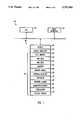
- the computer 20includes a CPU 22 which is coupled to user interface 24; the user interface 24 includes a keyboard, mouse, monitor, and printer.
- Memory 25is coupled to CPU 22 and user interface 24; memory 25 may be any combination of disk memory, RAM, and ROM.
- a netlist 26is stored within memory 25.
- a netlistcomprises a list of physical circuit components and the interconnections between those components.
- the netlist 26defines the interconnections between all functional elements in a physical circuit.
- a digital simulator 28is provided for this purpose.
- a number of commercially available digital simulatorsare known in the art, including Verilog and Hilo.
- Verilog and Hiloare known in the art, including Verilog and Hilo.
- the present inventionis disclosed in relation to a Verilog simulator and its corresponding syntax, however, as will be appreciated by one skilled in the art, the teachings of the invention are equally applicable to other digital simulators.
- the digital simulator 28includes a cell library 30.
- the cell library 30stores the attributes corresponding to the function of the individual physical circuit components.
- a typical digital simulatorincludes attribute information for an AND gate 32, a NOR gate 34, a counter 36, and a memory array 38.
- the AND gate cell 32represents a physical circuit element having the following attributes: it generates an output of ONE if its two inputs are ONE, otherwise its output is ZERO.
- the NOR gate cell 34represents a physical circuit element which generates an output of ONE if its two inputs are ZERO, otherwise its output is ZERO.
- the counter cell 36represents a physical circuit element which keeps track of the number of pulses applied to it.
- the output of the counter 36is a binary array of numbers, for instance a 16 bit array. This array can then be utilized directly by the circuit or converted to a decimal format for output for analysis by an operator of the digital simulator 28.
- Digital simulator 28also includes a memory array cell 38 which outputs a binary array of numbers.
- Digital simulator 28uses a full cell library 30 to model all physical digital components within a digital circuit. As is known in the art, digital simulators are capable of providing a complete simulation of a proposed circuit, as defined by the netlist, in a relatively short period of time. This time advantage stands in contrast to the time-consuming process of providing an analog simulation of a circuit.
- the cell library 30 of digital simulator 28is expanded to include models for analog circuit elements.
- the digital simulator 28 of the present inventionis not limited to digital components, but is expanded to include analog elements as well.
- Digital modeling of analog circuit componentsresults in a number of benefits. First, a rapid simulation of a physical circuit with analog elements is achieved. Next, the digital modeling of physical analog circuit elements obviates the necessity of running two separate simulations, one for the analog components of the circuit and one for the digital components of the circuit. In addition, the single digital simulation allows a unified analysis of the interaction between the digital and analog physical elements, including the effect of feedback between the separate domains.
- Models for a capacitor 40, a resistor ladder 42, a summation element 44, a comparator 46, and an analog voltage source 48are provided herein.
- FIG. 2A digital capacitor model in accordance with the present invention is disclosed in relation to FIGS. 2-5.
- FIG. 2an analog capacitor 50 is depicted.
- the analog capacitor 50is coupled to a switch 52 which may be moved to a number of voltage sources including Vin 54, v -- msb 56, and vdac 58.
- the output of the analog capacitor 50is shown herein as being coupled to a comparator 60.
- Analog capacitors 50are used in actual analog-to-digital converters to sample-and-hold analog input voltages and subtract algorithmically generated voltage levels from initially acquired voltages. The operation of such a capacitor 50 is depicted in relation to FIG. 3.
- the comparator 60is biased to its trip point Vtrip and "node a" of capacitor 50 is tied to Vin 54.
- Time t1is known as the auto zero and acquisition time.
- the comparator 60 output at "node b"is shorted to its input in order to bias the comparator.
- the trip pointis unobservable by the digital circuitry; therefore, Vtrip is assigned a zero value.
- the sampling of the input voltage and subsequent switching operationsdetermine the comparator output; consequently, it is necessary to model the charge redistributive properties of the capacitor 50.
- v -- msbis a value derived from a resistor ladder, which is not shown in this figure.
- the net voltage change at node b of capacitor 50is Vin-V -- msb. If Vin>V -- msb, the voltage change at node b is positive leading to a "1" output from the comparator 60. If Vin ⁇ V -- msb, the net result is negative leading to a comparator output of "0". Similarly, at time t3 the voltage at node b becomes Vin-Vdac, where Vdac is derived from another resistor ladder, which is not shown in this figure.
- the analog functionality of physical capacitor 50may be digitally modeled in accordance with the present invention.
- the storage capability of a capacitoris modeled through the use of vector-voltage registers 39.
- the vector-voltage registers 39are memory locations used by the simulator to store signal values. As in all simulators, registers are used to store all node voltages, as well as internal model values associated with each simulated circuit component.
- the vector-voltage registers 39 used for each capacitor elementare analogous to the binary arrays associated with counter 36 and memory array 38.
- all analog voltage signal pathsare 15-bit vector busses representing a dynamic range of +/-5 V.
- a sign bitis required since Verilog does not accept negative numbers. Therefore, when the vector-voltage is greater than 16,384, it is positive; conversely, vector-voltages less than 16,384 are negative.
- the vector-voltage representation of an analog signalis treated by Verilog either as an array of separate binary values or as an integer which may be manipulated in Verilog by addition, subtraction, multiplication, division, and equality. In other words, Verilog is already capable of performing mathematical operations on vectors of binary values. The present invention uses this vector handling capability to simulate analog signal processing.
- FIG. 4a digital capacitor model 70 in is depicted.
- the capacitor outputis dependent upon changes in the applied input vector-voltages.
- synchronizing input signalsare applied to the capacitor module to tell the capacitor when a new input voltage is present.
- Changes in t1, t2, and t3strobe the subtraction of the capacitor.
- the input of the capacitor "node a" 74 at time t1is stored in a register Rvin, at time t2 it is stored in register Rv -- msb, and at time t3 it is stored in Rvdac.
- An offset of 16384is added to set the positive sign bit, as described above.
- the input of the capacitor "node a" 74is tied to transmission gates 72.
- the transmission gates 72are represented by simple modules which pass the input vector-voltages Vin, V -- msb, and vdac when t1, t2, and t3 are respectively high. Otherwise, they are in a high impedance state.
- FIG. 5discloses the state table associated with digital capacitor 70. While t1 is high, a vector-voltage representation of Vin is multiplexed to "node a" 74. When clocking signal t1 goes low, register Rvin is set equal to the vector-voltage at "node a", in this case Vin. When t2 goes high, Vin is isolated from “node a" and v -- msb is multiplexed to "node a”. Verilog register Rv -- msb is set equal to "node a" 74 vector-voltage. The input to the digital comparator 80 "node b" 76 is set equal to:
- the zero ("0") denoted in the previous sentenceis actually a zero equivalent; that is, the most significant bit is set and an actual digital value of 16,384 is present, which corresponds to zero in the embodiment described herein.
- capacitor register Rvdacis set equal to the multiplexed voltage Vdac.
- the comparator inputbecomes:
- Verilog code suitable for executing these functionsis as follows:
- node a74 as a 15 bit input array and "node b" 76 as a 15 bit output array suitable for receiving vector-voltage values.
- Registers Rvin, Rv -- msb, and Rvdacare also defined as 15 bit arrays. "Node b" is then initialized by adding 16,384 to set the positive bit.
- the "b node”is then assigned the value of Rvin-Rv -- msb. Finally, at time t3, Rvdac receives the value of "node a" times 64 and "node b” receives the value of Rvin-Rvdac.
- the "#" notationrepresents a delay value to accommodate circuit signal propagation delay.
- resistor ladderAnother physical analog element modeled as a digital element in accordance with the present invention is the resistor ladder.
- the resistor ladderis an important analog component used to divide the reference voltage into discrete voltage quantities for use in the conversion algorithm.
- An actual resistor ladder containing B resistors spanning from 0 to Vrefdivides Vref into B+1 equal voltage steps. These voltages monotonically increase from resistor tap point to resistor tap point in Vref/B steps.
- Each resistor in a resistor laddermay be modeled for simulation purposes using the following Verilog code:
- inputs and outputsare defined as 15 bit registers for handling vector-voltages.
- the resistor output (Vout)is always the input plus a scale factor (sf).
- This scale factoris a vector-voltage equivalent to the voltage drop across the resistor.
- the lower vector-voltage of the resistor ladderwhich is the input to the first resistor, is fixed at 0 by a constant output vector source.
- the output of each resistordrives the input of the next. This results in an increase of the scale factor for each resistor output, resulting in an array of vector-voltages given by
- Multiplication scale factorsare used to convert this ladder of vector-voltages into levels of the appropriate magnitude, dependent upon the total voltage across the ladder Vref and the total length B.
- the scale factoris given by
- the scale factorcan be set to a value of 1 and the resulting voltages can be scaled when input to other circuit components.
- a summation element 100is depicted in relation to FIG. 8.
- the summation element 100may be used to add capacitive vector-voltage values.
- Simple Verilog code to realize a summation elementis as follows:
- the input and output valuesare defined as 15 bit arrays for handling vector-voltages.
- the output valueis simply the sum of the input nodes, which typically has no more than 12 bit values.
- Still another physical analog element which is modeled as a digital cell in accordance with the present inventionis a comparator.
- a comparator 110 in accordance with the present inventionis disclosed in relation to FIG. 9.
- An actual analog comparatoris a circuit which determines the inequality of two analog voltages. For the ideal comparator, if Vinp>Vinn the output is ONE. Conversely, if Vinp ⁇ Vinn, the output is a ZERO.
- the comparatoris the final interface between the analog circuit elements and the digital circuit elements in an actual analog-to-digital circuit.
- An actual analog comparatormay be modeled as a digital element in Verilog by using the following code:
- This modulecompares its two input array values and assigns a binary output of ONE if Vinp is greater than Vinn, otherwise it assigns a binary value of ZERO.
- a digital voltage source 120is depicted in FIG. 10.
- Suitable Verilog code for creating vector- voltagesis as follows:
- 16 distinct voltage source modelsare provided, as listed in FIG. 11.
- the table of FIG. 11provides a suitable analog-to-digital conversion scheme. Through these conversions, actual analog voltage values are converted to vector-voltages for use in the simulation of the actual circuit.
- the analog input Vais estimated by the thresholds of seven adjacent analog comparators 130.
- the outputis low (ZERO) for all analog comparators 130 with thresholds above the analog input voltage Va and high (ONE) for each comparator whose threshold is below the analog voltage input Va.
- An encoder 140converts the input pattern into a 3 bit digital value which corresponds to the analog voltage value.
- Capacitors 150may also be utilized to sample-and-hold the analog input voltages and subtract generated voltage levels from the initial acquired voltage.
- a trimming capacitor 152may also be provided.
- the ADC of FIG. 12is a simple embodiment for the purposes of illustration.
- Present ADCstypically include digital circuits for controlling successive passes by the analog circuits and obtain a much higher resolution than is possible from the exemplary ADC of FIG. 12.
- FIG. 13illustrates a portion 160 of the ADC of FIG. 12. More particularly, FIG. 13 depicts a digital model of the actual analog elements of an analog-to-digital converter.
- the actual analog comparatoris replaced with the digitally modeled comparator 110.
- the actual analog capacitor 150 and analog trimming capacitor 152are replaced with digitally modeled capacitors 70A and 70B.
- summation element 100is provided.
- the other input to digitally modeled comparator 110is digitally modeled capacitor 70C. Transmission gates 72 drive each of the capacitors 70A, 70B, and 70C.
- the digital simulator 28 of the present inventionincludes an expanded cell library 30 to accommodate digital equivalents of analog elements.
- This digital modelingrelies upon vector-voltage representations of analog voltage values.
- the netlist 26 fed to the digital simulatormay include analog elements and the entire simulation may be run in a digital simulation environment. Regardless of the complexity of the circuit, and despite the fact that both analog and digital components are present, a single integrated simulation of the entire circuit is rapidly executed.
Landscapes
- Engineering & Computer Science (AREA)
- Computer Hardware Design (AREA)
- Theoretical Computer Science (AREA)
- Physics & Mathematics (AREA)
- Evolutionary Computation (AREA)
- General Physics & Mathematics (AREA)
- General Engineering & Computer Science (AREA)
- Geometry (AREA)
- Microelectronics & Electronic Packaging (AREA)
- Mathematical Physics (AREA)
- Automation & Control Theory (AREA)
- Fuzzy Systems (AREA)
- Software Systems (AREA)
- Analogue/Digital Conversion (AREA)
Abstract
Description
This invention relates generally to devices which simulate the operation of circuits. More particularly, this invention relates to a method and apparatus for providing a digital simulation for a circuit which includes both analog and digital elements.
Electronic devices commonly include analog and digital elements. As a result, an analog-to-digital converter (ADC) is used to provide an interface between the two types of signals. Typical analog-to-digital converters include resistor ladders, capacitor arrays, sampled-data comparators, and analog multiplexers, as well as a variety of digital circuits. The digital and analog circuit elements may interact in many different ways. For instance, the digital circuitry may strobe comparators and drive analog multiplexers for routing of analog voltage levels. The analog elements often generate signals interfacing to the digital circuitry. Partitioning the analog and digital domains is difficult because of the existence of feedback signals between the two domains. Analog-to-digital converter architectures continue to grow in complexity as multiple steps and trimming algorithms are employed to obtain higher resolutions. Prior to physical implementation, these and other complex circuit designs are typically tested through a computerized simulation. Simulating a circuit with analog and digital components generally requires separate simulations of the analog and digital blocks.
There are a number of problems with this approach. Primarily, this approach does not detect errors at the interface between the two domains. This interface region of the circuit is susceptible to a number of problems. For instance, resistor tap-points may be off center, decoder or encoder values may be incorrect, capacitor ratios may be mismatched, or the availability of memory addresses may be mismatched with an address strobe. These problems, and others, are often encountered, but they are not detectable by using separate conventional digital and analog simulations.
In addition to the problem of detecting errors at the domain interface, prior art circuit simulation techniques are unsatisfactory to the extent that they rely upon analog simulations. Analog simulations are commonly run on simulators such as SPICE. These simulators are relatively slow. In contrast, digital simulators such as Verilog or Hilo are relatively fast.
Another difficulty associated with running separate simulations for the analog and digital components of a circuit is that the separate simulations do not account for feedback signals which may exist between the two blocks.
Mixed signal simulation design tools presently exist. However, these tools are complex and have not resulted in practical design verification tools.
Thus, it is a general object of the present invention to provide a single circuit simulator for both the analog and digital components of a circuit.
It is a related object of the present invention to provide a circuit simulator which is capable of detecting errors at the interface between digital and analog domains.
It is another object of the present invention to provide a circuit simulator which simulates both the analog and digital components of a circuit in a digital format.
It is a related object of the present invention to provide a fast mixed signal circuit simulator.
It is another object of the present invention to provide a circuit simulator which accounts for feedback signals between analog and digital domains.
These and other objects are achieved by a method and apparatus for providing a single digital simulation of a circuit with analog and digital components. A netlist characterizing a circuit with analog and digital components is utilized. The netlist defines each component in the circuit and its interconnections. The netlist is conveyed to a digital simulator which includes an expanded cell library. The cell library defines analog components in a digital manner. The digitally defined analog components process analog signals which are simulated as arrays of binary values, termed vector-voltages. The vector-voltages may be combined, mathematically or logically, with other vector- voltages to produce binary signals suitable as inputs to the digitally modeled analog circuit elements. In addition, vector-voltages can be converted, using circuit elements such as comparators, into digital logic signals suitable as inputs to digital circuit elements. Regardless of the complexity of the circuit, and despite the fact that both analog and digital components are present, a single integrated digital simulation of the entire circuit is rapidly executed by utilizing digital models of the analog components.
For a better understanding of the nature and objects of the invention, reference is made to the following detailed description taken in conjunction with the accompanying drawings, in which:
FIG. 1 is a block diagram of a general purpose computer which may used in accordance with the present invention.
FIG. 2 is a depiction of an analog capacitor coupled to a gate which switches the capacitor to a number of voltage sources.
FIG. 3 is a graph of voltage as a function of time for the capacitor of FIG. 2.
FIG. 4 is a depiction of a digital capacitor modeled in accordance with the present invention.
FIG. 5 is a table reflecting the various outputs of the digital capacitor of FIG. 4.
FIG. 6 is an analog voltage to digital voltage conversion model which may be used in accordance with a 16 bit embodiment of the present invention.
FIG. 7 is a depiction of a resistor ladder utilized in accordance with the present invention.
FIG. 8 is a depiction of a summation element utilized in accordance with the present invention.
FIG. 9 is a depiction of a comparator utilized in accordance with the present invention.
FIG. 10 is a depiction of a voltage source utilized in accordance with the present invention.
FIG. 11 is a table depicting appropriate analog to digital conversion values for a digital voltage source.
FIG. 12 is a schematic of a 3-bit parallel A/D converter.
FIG. 13 is a representation, in accordance with the present invention, of a portion of the A/D converter of FIG. 12.
Like reference numerals refer to corresponding parts throughout the several views of the drawings.
Referring to FIG. 1, ageneral purpose computer 20 which may be used in accordance with the present invention is depicted. Thecomputer 20 includes aCPU 22 which is coupled touser interface 24; theuser interface 24 includes a keyboard, mouse, monitor, and printer.Memory 25 is coupled toCPU 22 anduser interface 24;memory 25 may be any combination of disk memory, RAM, and ROM.
Anetlist 26 is stored withinmemory 25. As is known in the art, a netlist comprises a list of physical circuit components and the interconnections between those components. Thus, thenetlist 26 defines the interconnections between all functional elements in a physical circuit. By simulating the operation of the physical circuit represented by the netlist, the entire physical circuit can be tested for proper operation prior to fabrication.
Adigital simulator 28 is provided for this purpose. A number of commercially available digital simulators are known in the art, including Verilog and Hilo. For purposes of illustration, the present invention is disclosed in relation to a Verilog simulator and its corresponding syntax, however, as will be appreciated by one skilled in the art, the teachings of the invention are equally applicable to other digital simulators.
Thedigital simulator 28 includes acell library 30. Thecell library 30 stores the attributes corresponding to the function of the individual physical circuit components. Thus, by way of example, a typical digital simulator includes attribute information for an ANDgate 32, a NORgate 34, acounter 36, and amemory array 38. The ANDgate cell 32 represents a physical circuit element having the following attributes: it generates an output of ONE if its two inputs are ONE, otherwise its output is ZERO. The NORgate cell 34 represents a physical circuit element which generates an output of ONE if its two inputs are ZERO, otherwise its output is ZERO. Thecounter cell 36 represents a physical circuit element which keeps track of the number of pulses applied to it. The output of thecounter 36 is a binary array of numbers, for instance a 16 bit array. This array can then be utilized directly by the circuit or converted to a decimal format for output for analysis by an operator of thedigital simulator 28.Digital simulator 28 also includes amemory array cell 38 which outputs a binary array of numbers.
In accordance with the present invention, thecell library 30 ofdigital simulator 28 is expanded to include models for analog circuit elements. Thus, thedigital simulator 28 of the present invention is not limited to digital components, but is expanded to include analog elements as well. Digital modeling of analog circuit components results in a number of benefits. First, a rapid simulation of a physical circuit with analog elements is achieved. Next, the digital modeling of physical analog circuit elements obviates the necessity of running two separate simulations, one for the analog components of the circuit and one for the digital components of the circuit. In addition, the single digital simulation allows a unified analysis of the interaction between the digital and analog physical elements, including the effect of feedback between the separate domains.
In accordance with the present invention, digital models are provided for a number of physical analog components. Models for acapacitor 40, aresistor ladder 42, asummation element 44, acomparator 46, and ananalog voltage source 48 are provided herein.
A digital capacitor model in accordance with the present invention is disclosed in relation to FIGS. 2-5. Turning to FIG. 2, ananalog capacitor 50 is depicted. Theanalog capacitor 50 is coupled to aswitch 52 which may be moved to a number of voltagesources including Vin 54, v-- msb 56, andvdac 58. The output of theanalog capacitor 50 is shown herein as being coupled to acomparator 60.
At time t2, thecapacitor 50 is switched to voltage v-- msb 56. In this example, v-- msb is a value derived from a resistor ladder, which is not shown in this figure. The net voltage change at node b ofcapacitor 50 is Vin-V-- msb. If Vin>V-- msb, the voltage change at node b is positive leading to a "1" output from thecomparator 60. If Vin<V-- msb, the net result is negative leading to a comparator output of "0". Similarly, at time t3 the voltage at node b becomes Vin-Vdac, where Vdac is derived from another resistor ladder, which is not shown in this figure.
The analog functionality ofphysical capacitor 50 may be digitally modeled in accordance with the present invention. In particular, the storage capability of a capacitor is modeled through the use of vector-voltage registers 39. The vector-voltage registers 39 are memory locations used by the simulator to store signal values. As in all simulators, registers are used to store all node voltages, as well as internal model values associated with each simulated circuit component. The vector-voltage registers 39 used for each capacitor element are analogous to the binary arrays associated withcounter 36 andmemory array 38.
In accordance with the present invention, analog voltages are represented in simulators such as Verilog by a vector of binary values, called a vector-voltage herein. This is accomplished by replacing all analog paths with N-bit busses, where N defines the resolution of the analog voltage. Thus, in a 15 bit system, allowing 1 bit for polarity, N=15. If a 5 V system is being utilized, 0.31 mv resolution is possible. This modeling is depicted in relation to FIG. 6.
In a preferred embodiment, all analog voltage signal paths are 15-bit vector busses representing a dynamic range of +/-5 V. In order to allow negative voltages, a sign bit is required since Verilog does not accept negative numbers. Therefore, when the vector-voltage is greater than 16,384, it is positive; conversely, vector-voltages less than 16,384 are negative. The vector-voltage representation of an analog signal is treated by Verilog either as an array of separate binary values or as an integer which may be manipulated in Verilog by addition, subtraction, multiplication, division, and equality. In other words, Verilog is already capable of performing mathematical operations on vectors of binary values. The present invention uses this vector handling capability to simulate analog signal processing.
Turning to FIG. 4, a digital capacitor model 70 in is depicted. The capacitor output is dependent upon changes in the applied input vector-voltages. In order to sense a change in the input voltage, synchronizing input signals are applied to the capacitor module to tell the capacitor when a new input voltage is present. Changes in t1, t2, and t3 strobe the subtraction of the capacitor. The input of the capacitor "node a" 74 at time t1 is stored in a register Rvin, at time t2 it is stored in register Rv-- msb, and at time t3 it is stored in Rvdac. An offset of 16384 is added to set the positive sign bit, as described above.
The input of the capacitor "node a" 74 is tied totransmission gates 72. Thetransmission gates 72 are represented by simple modules which pass the input vector-voltages Vin, V-- msb, and vdac when t1, t2, and t3 are respectively high. Otherwise, they are in a high impedance state.
FIG. 5 discloses the state table associated with digital capacitor 70. While t1 is high, a vector-voltage representation of Vin is multiplexed to "node a" 74. When clocking signal t1 goes low, register Rvin is set equal to the vector-voltage at "node a", in this case Vin. When t2 goes high, Vin is isolated from "node a" and v-- msb is multiplexed to "node a". Verilog register Rv-- msb is set equal to "node a" 74 vector-voltage. The input to thedigital comparator 80 "node b" 76 is set equal to:
V("node b")=Rvin-Rv.sub.--msb+ 16384The digitally modeledcomparator 80, which will be further discussed below, outputs a digital "1" if V("node b")>0 and a "0" if V("node b")<=0. The zero ("0") denoted in the previous sentence is actually a zero equivalent; that is, the most significant bit is set and an actual digital value of 16,384 is present, which corresponds to zero in the embodiment described herein. Similarly, at time t3 capacitor register Rvdac is set equal to the multiplexed voltage Vdac. The comparator input becomes:
V("node b")=Rvin-Rvdac+ 16384Verilog code suitable for executing these functions is as follows:
______________________________________ module cap2.sub.-- v(a,b,t1,t2,t3) output[1:15]b; input[1:15]a; input t1,t2,t3; reg[1:15] b,Rv.sub.-- msb,Rvin,Rvdac; initial b=15'b16384; always @(negedge t1) begin #5 Rvin=1*a + 16384; end always @(posedge t2) begin #50 Rv.sub.-- msb=1*64*a; #2 b=Rvin-Rv.sub.-- msb; end always @(posedge t3) begin #50 Rvdac=1*64*a; #2 b= Rvin-Rvdac; end endmodule ______________________________________
The foregoing code initially defines "node a" 74 as a 15 bit input array and "node b" 76 as a 15 bit output array suitable for receiving vector-voltage values. Registers Rvin, Rv-- msb, and Rvdac are also defined as 15 bit arrays. "Node b" is then initialized by adding 16,384 to set the positive bit.
Three loops are then entered, one for each of the inputs t1, t2, and t3. At the t1 input Rvin becomes the value of "node a" plus 16,384. In this example, "node a" is multiplied by 1 because one capacitor is utilized before thecomparator 80, if 2 capacitors were utilized, then "node a" would be multiplied by 2 and so forth. At the t2 input, Rv-- msb becomes 64 times "node a". In this example 64 is multiplied by one because only one capacitor is present, if two capacitors are present, then 64 should be multiplied by 2 and so forth. Multiplication by 64 is undertaken for the purpose of scaling the vector-voltage value received from a resistor ladder (not shown). The "b node" is then assigned the value of Rvin-Rv-- msb. Finally, at time t3, Rvdac receives the value of "node a"times 64 and "node b" receives the value of Rvin-Rvdac. The "#" notation represents a delay value to accommodate circuit signal propagation delay.
Another physical analog element modeled as a digital element in accordance with the present invention is the resistor ladder. In actual analog-to-digital converters, the resistor ladder is an important analog component used to divide the reference voltage into discrete voltage quantities for use in the conversion algorithm. An actual resistor ladder containing B resistors spanning from 0 to Vref divides Vref into B+1 equal voltage steps. These voltages monotonically increase from resistor tap point to resistor tap point in Vref/B steps. Each resistor in a resistor ladder may be modeled for simulation purposes using the following Verilog code:
______________________________________ module resistor(vout,vin); output[1:15]vout; input[1:15]vin; reg[1:15]vout; initial forever begin #1 vout=vin + sf; end endmodule ______________________________________
In the module, inputs and outputs are defined as 15 bit registers for handling vector-voltages. The resistor output (Vout) is always the input plus a scale factor (sf). This scale factor is a vector-voltage equivalent to the voltage drop across the resistor. By stringing severalVerilog resistors 90 together, a monotonically increasing ladder of vector-voltages is modeled, as can be appreciated in relation to FIG. 7.
The lower vector-voltage of the resistor ladder, which is the input to the first resistor, is fixed at 0 by a constant output vector source. The output of each resistor drives the input of the next. This results in an increase of the scale factor for each resistor output, resulting in an array of vector-voltages given by
VV(sf)={1,2,3,4,5, . . . ,B} * sfMultiplication scale factors are used to convert this ladder of vector-voltages into levels of the appropriate magnitude, dependent upon the total voltage across the ladder Vref and the total length B. The scale factor is given by
sf=16384/(L * B)
where B is the number of resistors spanning the voltage range Vref/L and L is the fraction of the full scale range which the resistor ladder spans. Alternately, the scale factor can be set to a value of 1 and the resulting voltages can be scaled when input to other circuit components.
Other physical circuit elements which need a digital model include a summation element, a comparator, and a voltage source. Asummation element 100 is depicted in relation to FIG. 8. Thesummation element 100 may be used to add capacitive vector-voltage values. Simple Verilog code to realize a summation element is as follows:
______________________________________ module sumnode.sub.-- v(a,b,c,d,e,out); output[1:15]out; input[1:15]a,b,c,d,e; reg[1:15]out; initial forever begin #1 out=a+b+c+d+e; end endmodule ______________________________________
The input and output values are defined as 15 bit arrays for handling vector-voltages. The output value is simply the sum of the input nodes, which typically has no more than 12 bit values.
Still another physical analog element which is modeled as a digital cell in accordance with the present invention is a comparator. Acomparator 110 in accordance with the present invention is disclosed in relation to FIG. 9. An actual analog comparator is a circuit which determines the inequality of two analog voltages. For the ideal comparator, if Vinp>Vinn the output is ONE. Conversely, if Vinp<Vinn, the output is a ZERO.
The comparator is the final interface between the analog circuit elements and the digital circuit elements in an actual analog-to-digital circuit. An actual analog comparator may be modeled as a digital element in Verilog by using the following code:
______________________________________ module comparator.sub.-- v(vinp,vinn,out); output out; input[1:15] vinp,vinn; reg out; initial begin if(vinp>vinn) #2 out=1; else #1 out=0; end endmodule ______________________________________
This module compares its two input array values and assigns a binary output of ONE if Vinp is greater than Vinn, otherwise it assigns a binary value of ZERO.
Yet another analog physical element which is modeled as a digital element in accordance with the present invention is a voltage source. Adigital voltage source 120 is depicted in FIG. 10. Suitable Verilog code for creating vector- voltages is as follows:
______________________________________ module v4(vout); output[1:15]vout; reg[1:15]vout; initial vout=15'd4; endmodule ______________________________________
This module corresponds to the analog-to-digital voltage conversion of N=4 in the table depicted in FIG. 11. In the preferred embodiment, 16 distinct voltage source models are provided, as listed in FIG. 11. The table of FIG. 11 provides a suitable analog-to-digital conversion scheme. Through these conversions, actual analog voltage values are converted to vector-voltages for use in the simulation of the actual circuit.
Turning now to FIG. 12, an actual 3-bit parallel ADC is depicted. The analog input Va is estimated by the thresholds of sevenadjacent analog comparators 130. The output is low (ZERO) for allanalog comparators 130 with thresholds above the analog input voltage Va and high (ONE) for each comparator whose threshold is below the analog voltage input Va. Anencoder 140 converts the input pattern into a 3 bit digital value which corresponds to the analog voltage value.
The ADC of FIG. 12 is a simple embodiment for the purposes of illustration. Present ADCs typically include digital circuits for controlling successive passes by the analog circuits and obtain a much higher resolution than is possible from the exemplary ADC of FIG. 12.
In any event, FIG. 13 illustrates aportion 160 of the ADC of FIG. 12. More particularly, FIG. 13 depicts a digital model of the actual analog elements of an analog-to-digital converter. The actual analog comparator is replaced with the digitally modeledcomparator 110. Theactual analog capacitor 150 andanalog trimming capacitor 152 are replaced with digitally modeledcapacitors 70A and 70B. To achieve the summing of the vector-voltages of these capacitive components,summation element 100 is provided. The other input to digitally modeledcomparator 110 is digitally modeledcapacitor 70C.Transmission gates 72 drive each of thecapacitors
Thus, thedigital simulator 28 of the present invention includes an expandedcell library 30 to accommodate digital equivalents of analog elements. This digital modeling relies upon vector-voltage representations of analog voltage values. As a result of this modeling, thenetlist 26 fed to the digital simulator may include analog elements and the entire simulation may be run in a digital simulation environment. Regardless of the complexity of the circuit, and despite the fact that both analog and digital components are present, a single integrated simulation of the entire circuit is rapidly executed.
The foregoing descriptions of specific embodiments of the present invention have been presented for purposes of illustration and description. They are not intended to be exhaustive or to limit the invention to the precise forms disclosed, and obviously many modifications and variations are possible in light of the above teaching. The embodiments were chosen and described in order to best explain the principles of the invention and its practical application, to thereby enable others skilled in the art to best utilize the invention and various embodiments with various modifications as are suited to the particular use contemplated. It is intended that the scope of the invention be defined by the claims appended hereto and their equivalents.
Claims (13)
1. A method of digitally simulating the operation of an electronic circuit having both analog and digital components, said method comprising the steps of:
storing in a memory module of a data processor a netlist representing a specified electronic circuit, said netlist containing a list of analog and digital circuit components and corresponding connections for each of said components;
retrieving from a cell library stored in said memory module of said data processor, digital circuit models for each of said analog and digital circuit components in said netlist; and
simulating the operation of said specified electronic circuit on a digital circuit simulator that simulates said specified electronic circuit with said digital circuit models, said simulation step including representing each analog signal received and processed by said specified electronic circuit as a vector of binary signal values.
2. The method of claim 1 wherein at least one of said digital circuit models in said cell library represents an analog circuit component which receives at least one analog input signal represented as a vector of binary signal values and which outputs at least one separate binary signal suitable for use as an input signal to a digital circuit component.
3. The method of claim 1 wherein said representing step includes providing at least an 8 bit vector of binary signal values for each of said analog signals.
4. The method of claim 1 wherein said retrieving step includes supplying a digitally modeled capacitor, voltage source, and comparator.
5. The method of claim 1 wherein said retrieving step includes supplying a digitally modeled resistor ladder and summing element.
6. A method of digitally simulating on a digital circuit simulator the operation of an electronic circuit having both analog and digital components, said method comprising the steps of:
storing in a memory module of a data processor a netlist representing a specified electronic circuit, said netlist containing a list of analog and digital circuit components and corresponding connections for each of said components;
converting each of said analog and digital circuit components in said netlist to a corresponding digital circuit model comprising a set of specified mathematical relationships between binary input and binary output signals; and
simulating the operation of said specified electronic circuit with said digital circuit models, said simulating step including representing analog input signals into said specified circuit and analog signals generated by said analog circuit components as a vector of binary signal values.
7. The method of claim 6 wherein said representing step includes providing at least a 8 bit vector of binary signal values for each of said analog signals.
8. The method of claim 7 wherein said converting step includes supplying a digitally modeled capacitor, voltage source, and comparator.
9. The method of claim 7 wherein said converting step includes supplying a digitally modeled resistor ladder and summing element.
10. The method of claim 8 wherein said digital capacitor includes three time inputs, t1, t2, and t3, the operation of said digital capacitor including the steps of subtracting a first voltage value from a Vinput value at time 2 and subtracting a second voltage value from said Vinput value at time 3.
11. An apparatus for simulating the operation of an actual circuit which includes digital and analog components, said apparatus comprising:
means for storing a netlist defining an actual circuit including a plurality of digital and analog circuit components and their corresponding interconnections; and
means for analyzing said netlist, said analyzing means including
means for defining analog voltage values received and processed by said actual electronic circuit as vector-voltage values, and
means for providing digital representations of said analog components, whereby said analyzing means provides a single digital simulation of the operation of an actual circuit with analog and digital components.
12. The apparatus of claim 11 wherein said analyzing means includes a digital simulator with an expanded cell library including modeled digital capacitors, digital resistors, digital comparators, digital voltage sources, and digital summation elements.
13. The apparatus of claim 12 wherein said analyzing means includes a CPU, a user interface coupled to said CPU, and memory means coupled to said CPU and said user interface, said memory means storing said netlist, said digital simulator, and said cell library.
Priority Applications (1)
| Application Number | Priority Date | Filing Date | Title |
|---|---|---|---|
| US07/780,775US5297066A (en) | 1991-10-22 | 1991-10-22 | Digital circuit simulation of analog/digital circuits |
Applications Claiming Priority (1)
| Application Number | Priority Date | Filing Date | Title |
|---|---|---|---|
| US07/780,775US5297066A (en) | 1991-10-22 | 1991-10-22 | Digital circuit simulation of analog/digital circuits |
Publications (1)
| Publication Number | Publication Date |
|---|---|
| US5297066Atrue US5297066A (en) | 1994-03-22 |
Family
ID=25120659
Family Applications (1)
| Application Number | Title | Priority Date | Filing Date |
|---|---|---|---|
| US07/780,775Expired - LifetimeUS5297066A (en) | 1991-10-22 | 1991-10-22 | Digital circuit simulation of analog/digital circuits |
Country Status (1)
| Country | Link |
|---|---|
| US (1) | US5297066A (en) |
Cited By (27)
| Publication number | Priority date | Publication date | Assignee | Title |
|---|---|---|---|---|
| US5414639A (en)* | 1993-01-19 | 1995-05-09 | Sony Corporation | Automatic testing method and testing apparatus for devices |
| US5477474A (en)* | 1992-10-29 | 1995-12-19 | Altera Corporation | Computer logic simulation with dynamic modeling |
| US5481484A (en)* | 1991-10-09 | 1996-01-02 | Hitachi, Ltd. | Mixed mode simulation method and simulator |
| US5499192A (en)* | 1991-10-30 | 1996-03-12 | Xilinx, Inc. | Method for generating logic modules from a high level block diagram |
| US5535146A (en)* | 1995-04-27 | 1996-07-09 | National Science Council Of R.O.C. | Method for producing a semiconductor device using logic simulation approach to simulate a multi-peak resonant tunneling diode-based electronic circuit and a large signal multi-peak resonant tunneling diode spice model employed therefore |
| US5617326A (en)* | 1993-03-15 | 1997-04-01 | Kabushiki Kaisha Toshiba | Electronic circuit analyzing method with automatic adjustment of feedback loop effects |
| US5646515A (en)* | 1994-01-19 | 1997-07-08 | National Semiconductor Corporation | Ratioed reference voltage generation using self-correcting capacitor ratio and voltage coefficient error |
| US5675502A (en)* | 1995-08-22 | 1997-10-07 | Quicklogic Corporation | Estimating propagation delays in a programmable device |
| US5872908A (en)* | 1995-05-31 | 1999-02-16 | Texas Instruments Incorporated | IC with isolated analog signal path for testing |
| US5889685A (en)* | 1996-08-02 | 1999-03-30 | Cirrus Logic, Inc. | Method and apparatus for automatically characterizing short circuit current and power consumption in a digital circuit |
| US5910958A (en)* | 1991-08-14 | 1999-06-08 | Vlsi Technology, Inc. | Automatic generation of test vectors for sequential circuits |
| US5991522A (en)* | 1997-03-14 | 1999-11-23 | Fujitsu Limited | Method and apparatus for circuit conversion for simulation, simulator using the same, and computer-readable medium with a program therefor stored thereon |
| US6110217A (en)* | 1997-10-03 | 2000-08-29 | International Business Machines Corporation | System and method for synchronization of multiple analog servers on a simulation backplane |
| US6266630B1 (en)* | 1998-06-03 | 2001-07-24 | Mentor Graphics Corporation | Method and apparatus for providing a graphical user interface for simulating designs with analog and mixed signals |
| GB2362728A (en)* | 1999-10-29 | 2001-11-28 | Sgs Thomson Microelectronics | Verifying the accuracy of a digital model of an integrated circuit |
| WO2002003310A1 (en)* | 2000-07-05 | 2002-01-10 | Meyer Steven J | Mixed signal simulation |
| US20020022950A1 (en)* | 2000-06-08 | 2002-02-21 | Peter Ballam | Method and system for identifying inaccurate models |
| US6353915B1 (en) | 1999-04-01 | 2002-03-05 | Unisys Corporation | Methods for evaluating systems of electronic components |
| US6408264B1 (en) | 1999-03-23 | 2002-06-18 | Vanguard International Semiconductor-America | Switch level simulation with cross-coupled devices |
| US20030025712A1 (en)* | 2001-08-06 | 2003-02-06 | Corr William E. | Interpolation error minimization for data reduction |
| US20030154061A1 (en)* | 2001-11-21 | 2003-08-14 | Willis John Christopher | Method for semi-automatic generation and behavioral comparison of models |
| US20030188275A1 (en)* | 2002-03-27 | 2003-10-02 | Meares Lawrence G. | System and method of preventing the simulation of a circuit if a change to the circuit topology is detected |
| US7110929B1 (en)* | 1999-11-12 | 2006-09-19 | Intusoft | System and method of providing additional circuit analysis using simulation templates |
| US20090228849A1 (en)* | 2008-03-05 | 2009-09-10 | Mossawir Kathryn M | Method for Using an Equivalence Checker to Reduce Verification Effort in a System Having Analog Blocks |
| US20100023308A1 (en)* | 2001-11-21 | 2010-01-28 | Ftl Systems, Inc. | Method for accelerating simulation performance and increasing simulation accuracy of models using dynamic selection and replacement of executable embodiments with temporally optimal functional detail and simplification |
| US8296699B1 (en)* | 2010-02-26 | 2012-10-23 | Cadence Design Systems, Inc. | Method and system for supporting both analog and digital signal traffic on a single hierarchical connection for mixed-signal verification |
| US20230281366A1 (en)* | 2022-03-02 | 2023-09-07 | Taiwan Semiconductor Manufacturing Company, Ltd. | Apparatus and method of optimizing an integrtted circuit design |
Citations (2)
| Publication number | Priority date | Publication date | Assignee | Title |
|---|---|---|---|---|
| US5084824A (en)* | 1990-03-29 | 1992-01-28 | National Semiconductor Corporation | Simulation model generation from a physical data base of a combinatorial circuit |
| US5105373A (en)* | 1990-01-22 | 1992-04-14 | Texas Instruments Incorporated | Method of simulating the operation of a circuit having analog and digital circuit parts |
- 1991
- 1991-10-22USUS07/780,775patent/US5297066A/ennot_activeExpired - Lifetime
Patent Citations (2)
| Publication number | Priority date | Publication date | Assignee | Title |
|---|---|---|---|---|
| US5105373A (en)* | 1990-01-22 | 1992-04-14 | Texas Instruments Incorporated | Method of simulating the operation of a circuit having analog and digital circuit parts |
| US5084824A (en)* | 1990-03-29 | 1992-01-28 | National Semiconductor Corporation | Simulation model generation from a physical data base of a combinatorial circuit |
Cited By (38)
| Publication number | Priority date | Publication date | Assignee | Title |
|---|---|---|---|---|
| US5910958A (en)* | 1991-08-14 | 1999-06-08 | Vlsi Technology, Inc. | Automatic generation of test vectors for sequential circuits |
| US5481484A (en)* | 1991-10-09 | 1996-01-02 | Hitachi, Ltd. | Mixed mode simulation method and simulator |
| US5499192A (en)* | 1991-10-30 | 1996-03-12 | Xilinx, Inc. | Method for generating logic modules from a high level block diagram |
| US5477474A (en)* | 1992-10-29 | 1995-12-19 | Altera Corporation | Computer logic simulation with dynamic modeling |
| US5574893A (en)* | 1992-10-29 | 1996-11-12 | Altera Corporation | Computer logic simulation with dynamic modeling |
| US5414639A (en)* | 1993-01-19 | 1995-05-09 | Sony Corporation | Automatic testing method and testing apparatus for devices |
| US5617326A (en)* | 1993-03-15 | 1997-04-01 | Kabushiki Kaisha Toshiba | Electronic circuit analyzing method with automatic adjustment of feedback loop effects |
| US5646515A (en)* | 1994-01-19 | 1997-07-08 | National Semiconductor Corporation | Ratioed reference voltage generation using self-correcting capacitor ratio and voltage coefficient error |
| US5654713A (en)* | 1994-01-19 | 1997-08-05 | National Semiconductor Corporation | N-bit analog-to-digital converter having ratioed reference voltage generation using self-correcting capacitor ratio and voltage coefficient error |
| US5535146A (en)* | 1995-04-27 | 1996-07-09 | National Science Council Of R.O.C. | Method for producing a semiconductor device using logic simulation approach to simulate a multi-peak resonant tunneling diode-based electronic circuit and a large signal multi-peak resonant tunneling diode spice model employed therefore |
| US5872908A (en)* | 1995-05-31 | 1999-02-16 | Texas Instruments Incorporated | IC with isolated analog signal path for testing |
| US5675502A (en)* | 1995-08-22 | 1997-10-07 | Quicklogic Corporation | Estimating propagation delays in a programmable device |
| US5889685A (en)* | 1996-08-02 | 1999-03-30 | Cirrus Logic, Inc. | Method and apparatus for automatically characterizing short circuit current and power consumption in a digital circuit |
| US5991522A (en)* | 1997-03-14 | 1999-11-23 | Fujitsu Limited | Method and apparatus for circuit conversion for simulation, simulator using the same, and computer-readable medium with a program therefor stored thereon |
| US6110217A (en)* | 1997-10-03 | 2000-08-29 | International Business Machines Corporation | System and method for synchronization of multiple analog servers on a simulation backplane |
| US6266630B1 (en)* | 1998-06-03 | 2001-07-24 | Mentor Graphics Corporation | Method and apparatus for providing a graphical user interface for simulating designs with analog and mixed signals |
| US6408264B1 (en) | 1999-03-23 | 2002-06-18 | Vanguard International Semiconductor-America | Switch level simulation with cross-coupled devices |
| US6353915B1 (en) | 1999-04-01 | 2002-03-05 | Unisys Corporation | Methods for evaluating systems of electronic components |
| GB2362728A (en)* | 1999-10-29 | 2001-11-28 | Sgs Thomson Microelectronics | Verifying the accuracy of a digital model of an integrated circuit |
| GB2362728B (en)* | 1999-10-29 | 2002-04-24 | Sgs Thomson Microelectronics | A method of verifying the accuracy of a digital model |
| US7110929B1 (en)* | 1999-11-12 | 2006-09-19 | Intusoft | System and method of providing additional circuit analysis using simulation templates |
| US20020022950A1 (en)* | 2000-06-08 | 2002-02-21 | Peter Ballam | Method and system for identifying inaccurate models |
| US6996513B2 (en)* | 2000-06-08 | 2006-02-07 | Stmicroelectronics Limited | Method and system for identifying inaccurate models |
| US20020049576A1 (en)* | 2000-07-05 | 2002-04-25 | Meyer Steven J. | Digital and analog mixed signal simulation using PLI API |
| WO2002003310A1 (en)* | 2000-07-05 | 2002-01-10 | Meyer Steven J | Mixed signal simulation |
| US20030025712A1 (en)* | 2001-08-06 | 2003-02-06 | Corr William E. | Interpolation error minimization for data reduction |
| WO2003014963A1 (en)* | 2001-08-06 | 2003-02-20 | Micron Technology, Inc. | Interpolation error minimization for data reduction |
| US7072812B2 (en) | 2001-08-06 | 2006-07-04 | Micron Technology, Inc. | Interpolation error minimization for data reduction |
| US20100023308A1 (en)* | 2001-11-21 | 2010-01-28 | Ftl Systems, Inc. | Method for accelerating simulation performance and increasing simulation accuracy of models using dynamic selection and replacement of executable embodiments with temporally optimal functional detail and simplification |
| US20030154061A1 (en)* | 2001-11-21 | 2003-08-14 | Willis John Christopher | Method for semi-automatic generation and behavioral comparison of models |
| US7328195B2 (en) | 2001-11-21 | 2008-02-05 | Ftl Systems, Inc. | Semi-automatic generation of behavior models continuous value using iterative probing of a device or existing component model |
| US7539602B2 (en) | 2001-11-21 | 2009-05-26 | Ftl Systems, Inc. | Accelerating simulation of differential equation systems having continuous behavior |
| US20030188275A1 (en)* | 2002-03-27 | 2003-10-02 | Meares Lawrence G. | System and method of preventing the simulation of a circuit if a change to the circuit topology is detected |
| US20090228849A1 (en)* | 2008-03-05 | 2009-09-10 | Mossawir Kathryn M | Method for Using an Equivalence Checker to Reduce Verification Effort in a System Having Analog Blocks |
| US8117576B2 (en)* | 2008-03-05 | 2012-02-14 | Rambus Inc. | Method for using an equivalence checker to reduce verification effort in a system having analog blocks |
| US8296699B1 (en)* | 2010-02-26 | 2012-10-23 | Cadence Design Systems, Inc. | Method and system for supporting both analog and digital signal traffic on a single hierarchical connection for mixed-signal verification |
| US20230281366A1 (en)* | 2022-03-02 | 2023-09-07 | Taiwan Semiconductor Manufacturing Company, Ltd. | Apparatus and method of optimizing an integrtted circuit design |
| US12387022B2 (en)* | 2022-03-02 | 2025-08-12 | Taiwan Semiconductor Manufacturing Company, Ltd. | Apparatus and method of optimizing an integrated circuit design |
Similar Documents
| Publication | Publication Date | Title |
|---|---|---|
| US5297066A (en) | Digital circuit simulation of analog/digital circuits | |
| US20220100255A1 (en) | Unit Element for performing Multiply-Accumulate Operations | |
| US5382955A (en) | Error tolerant thermometer-to-binary encoder | |
| US7605738B2 (en) | A-D converter and A-D convert method | |
| US20080143574A1 (en) | A-D converter, A-D convert method, and A-D convert program | |
| Gielen et al. | CAD tools for data converter design: An overview | |
| Ruan | A behavioral model of A/D converters using a mixed-mode simulator | |
| KR950012977B1 (en) | D/a converter | |
| US5373292A (en) | Integration type D-A/A-D Conversion apparatus capable of shortening conversion processing time | |
| Liu et al. | A Behavioral Representation for Nyquist Rate A/D Converters. | |
| Bonnerud et al. | A mixed-signal, functional level simulation framework based on SystemC for system-on-a-chip applications | |
| Horta | Analogue and mixed-signal systems topologies exploration using symbolic methods | |
| US6304203B1 (en) | Successive approximation AD converter and microcomputer incorporating the same | |
| EP0858163B1 (en) | Pulse width modulation operation circuit | |
| JP2017158004A (en) | Temporary storage buffer device | |
| US4665382A (en) | Analog-to-digital conversion | |
| Bellavin et al. | Study of Bubble Errors Conversion in a Modified ROM Encoder | |
| JPS63501671A (en) | Untrimmed 12-bit monotonic full capacitive A/D converter | |
| JP2917095B2 (en) | Thermometer code processing method and apparatus | |
| Pandey et al. | Split Topology Based 8-Bit Flash ADC Architecture for Reduced Conversion Time | |
| Ponce-Hinestroza et al. | System-level behavioral model of a 12-bit 1.5-bit per stage pipelined ADC based on Verilog®=-AMS | |
| JPH04235418A (en) | AD converter | |
| RU2205500C1 (en) | Analog-to-digital converter | |
| RU2187884C1 (en) | Analog-to-digital converter | |
| RU182312U1 (en) | ANALOG-DIGITAL CONVERTER |
Legal Events
| Date | Code | Title | Description |
|---|---|---|---|
| AS | Assignment | Owner name:NATIONAL SEMICONDUCTOR CORPORATION A CORPORATION Free format text:ASSIGNMENT OF ASSIGNORS INTEREST.;ASSIGNOR:MAYES, MICHAEL K.;REEL/FRAME:005893/0724 Effective date:19911017 Owner name:NATIONAL SEMICONDUCTOR CORPORATION, A CORPORATION Free format text:ASSIGNMENT OF ASSIGNORS INTEREST;ASSIGNOR:MAYES, MICHAEL K.;REEL/FRAME:005893/0724 Effective date:19911017 | |
| STCF | Information on status: patent grant | Free format text:PATENTED CASE | |
| FPAY | Fee payment | Year of fee payment:4 | |
| FEPP | Fee payment procedure | Free format text:PAYOR NUMBER ASSIGNED (ORIGINAL EVENT CODE: ASPN); ENTITY STATUS OF PATENT OWNER: LARGE ENTITY | |
| FPAY | Fee payment | Year of fee payment:8 | |
| FPAY | Fee payment | Year of fee payment:12 |