US5296738A - Moisture relief for chip carrier - Google Patents
Moisture relief for chip carrierDownload PDFInfo
- Publication number
- US5296738A US5296738AUS07/927,774US92777492AUS5296738AUS 5296738 AUS5296738 AUS 5296738AUS 92777492 AUS92777492 AUS 92777492AUS 5296738 AUS5296738 AUS 5296738A
- Authority
- US
- United States
- Prior art keywords
- semiconductor die
- substrate
- printed circuit
- chip carrier
- package
- Prior art date
- Legal status (The legal status is an assumption and is not a legal conclusion. Google has not performed a legal analysis and makes no representation as to the accuracy of the status listed.)
- Expired - Lifetime
Links
Images


Classifications
- H—ELECTRICITY
- H01—ELECTRIC ELEMENTS
- H01L—SEMICONDUCTOR DEVICES NOT COVERED BY CLASS H10
- H01L23/00—Details of semiconductor or other solid state devices
- H01L23/564—Details not otherwise provided for, e.g. protection against moisture
- H—ELECTRICITY
- H01—ELECTRIC ELEMENTS
- H01L—SEMICONDUCTOR DEVICES NOT COVERED BY CLASS H10
- H01L23/00—Details of semiconductor or other solid state devices
- H01L23/12—Mountings, e.g. non-detachable insulating substrates
- H01L23/13—Mountings, e.g. non-detachable insulating substrates characterised by the shape
- H—ELECTRICITY
- H01—ELECTRIC ELEMENTS
- H01L—SEMICONDUCTOR DEVICES NOT COVERED BY CLASS H10
- H01L23/00—Details of semiconductor or other solid state devices
- H01L23/28—Encapsulations, e.g. encapsulating layers, coatings, e.g. for protection
- H01L23/31—Encapsulations, e.g. encapsulating layers, coatings, e.g. for protection characterised by the arrangement or shape
- H01L23/3107—Encapsulations, e.g. encapsulating layers, coatings, e.g. for protection characterised by the arrangement or shape the device being completely enclosed
- H01L23/3121—Encapsulations, e.g. encapsulating layers, coatings, e.g. for protection characterised by the arrangement or shape the device being completely enclosed a substrate forming part of the encapsulation
- H—ELECTRICITY
- H01—ELECTRIC ELEMENTS
- H01L—SEMICONDUCTOR DEVICES NOT COVERED BY CLASS H10
- H01L24/00—Arrangements for connecting or disconnecting semiconductor or solid-state bodies; Methods or apparatus related thereto
- H01L24/01—Means for bonding being attached to, or being formed on, the surface to be connected, e.g. chip-to-package, die-attach, "first-level" interconnects; Manufacturing methods related thereto
- H01L24/26—Layer connectors, e.g. plate connectors, solder or adhesive layers; Manufacturing methods related thereto
- H01L24/28—Structure, shape, material or disposition of the layer connectors prior to the connecting process
- H01L24/29—Structure, shape, material or disposition of the layer connectors prior to the connecting process of an individual layer connector
- H—ELECTRICITY
- H01—ELECTRIC ELEMENTS
- H01L—SEMICONDUCTOR DEVICES NOT COVERED BY CLASS H10
- H01L24/00—Arrangements for connecting or disconnecting semiconductor or solid-state bodies; Methods or apparatus related thereto
- H01L24/80—Methods for connecting semiconductor or other solid state bodies using means for bonding being attached to, or being formed on, the surface to be connected
- H01L24/83—Methods for connecting semiconductor or other solid state bodies using means for bonding being attached to, or being formed on, the surface to be connected using a layer connector
- H—ELECTRICITY
- H01—ELECTRIC ELEMENTS
- H01L—SEMICONDUCTOR DEVICES NOT COVERED BY CLASS H10
- H01L2224/00—Indexing scheme for arrangements for connecting or disconnecting semiconductor or solid-state bodies and methods related thereto as covered by H01L24/00
- H01L2224/01—Means for bonding being attached to, or being formed on, the surface to be connected, e.g. chip-to-package, die-attach, "first-level" interconnects; Manufacturing methods related thereto
- H01L2224/26—Layer connectors, e.g. plate connectors, solder or adhesive layers; Manufacturing methods related thereto
- H01L2224/28—Structure, shape, material or disposition of the layer connectors prior to the connecting process
- H01L2224/29—Structure, shape, material or disposition of the layer connectors prior to the connecting process of an individual layer connector
- H01L2224/29001—Core members of the layer connector
- H01L2224/29099—Material
- H01L2224/2919—Material with a principal constituent of the material being a polymer, e.g. polyester, phenolic based polymer, epoxy
- H—ELECTRICITY
- H01—ELECTRIC ELEMENTS
- H01L—SEMICONDUCTOR DEVICES NOT COVERED BY CLASS H10
- H01L2224/00—Indexing scheme for arrangements for connecting or disconnecting semiconductor or solid-state bodies and methods related thereto as covered by H01L24/00
- H01L2224/01—Means for bonding being attached to, or being formed on, the surface to be connected, e.g. chip-to-package, die-attach, "first-level" interconnects; Manufacturing methods related thereto
- H01L2224/26—Layer connectors, e.g. plate connectors, solder or adhesive layers; Manufacturing methods related thereto
- H01L2224/31—Structure, shape, material or disposition of the layer connectors after the connecting process
- H01L2224/32—Structure, shape, material or disposition of the layer connectors after the connecting process of an individual layer connector
- H01L2224/321—Disposition
- H01L2224/32151—Disposition the layer connector connecting between a semiconductor or solid-state body and an item not being a semiconductor or solid-state body, e.g. chip-to-substrate, chip-to-passive
- H01L2224/32221—Disposition the layer connector connecting between a semiconductor or solid-state body and an item not being a semiconductor or solid-state body, e.g. chip-to-substrate, chip-to-passive the body and the item being stacked
- H01L2224/32225—Disposition the layer connector connecting between a semiconductor or solid-state body and an item not being a semiconductor or solid-state body, e.g. chip-to-substrate, chip-to-passive the body and the item being stacked the item being non-metallic, e.g. insulating substrate with or without metallisation
- H—ELECTRICITY
- H01—ELECTRIC ELEMENTS
- H01L—SEMICONDUCTOR DEVICES NOT COVERED BY CLASS H10
- H01L2224/00—Indexing scheme for arrangements for connecting or disconnecting semiconductor or solid-state bodies and methods related thereto as covered by H01L24/00
- H01L2224/01—Means for bonding being attached to, or being formed on, the surface to be connected, e.g. chip-to-package, die-attach, "first-level" interconnects; Manufacturing methods related thereto
- H01L2224/42—Wire connectors; Manufacturing methods related thereto
- H01L2224/47—Structure, shape, material or disposition of the wire connectors after the connecting process
- H01L2224/48—Structure, shape, material or disposition of the wire connectors after the connecting process of an individual wire connector
- H01L2224/4805—Shape
- H01L2224/4809—Loop shape
- H01L2224/48091—Arched
- H—ELECTRICITY
- H01—ELECTRIC ELEMENTS
- H01L—SEMICONDUCTOR DEVICES NOT COVERED BY CLASS H10
- H01L2224/00—Indexing scheme for arrangements for connecting or disconnecting semiconductor or solid-state bodies and methods related thereto as covered by H01L24/00
- H01L2224/01—Means for bonding being attached to, or being formed on, the surface to be connected, e.g. chip-to-package, die-attach, "first-level" interconnects; Manufacturing methods related thereto
- H01L2224/42—Wire connectors; Manufacturing methods related thereto
- H01L2224/47—Structure, shape, material or disposition of the wire connectors after the connecting process
- H01L2224/48—Structure, shape, material or disposition of the wire connectors after the connecting process of an individual wire connector
- H01L2224/481—Disposition
- H01L2224/48135—Connecting between different semiconductor or solid-state bodies, i.e. chip-to-chip
- H01L2224/48137—Connecting between different semiconductor or solid-state bodies, i.e. chip-to-chip the bodies being arranged next to each other, e.g. on a common substrate
- H—ELECTRICITY
- H01—ELECTRIC ELEMENTS
- H01L—SEMICONDUCTOR DEVICES NOT COVERED BY CLASS H10
- H01L2224/00—Indexing scheme for arrangements for connecting or disconnecting semiconductor or solid-state bodies and methods related thereto as covered by H01L24/00
- H01L2224/01—Means for bonding being attached to, or being formed on, the surface to be connected, e.g. chip-to-package, die-attach, "first-level" interconnects; Manufacturing methods related thereto
- H01L2224/42—Wire connectors; Manufacturing methods related thereto
- H01L2224/47—Structure, shape, material or disposition of the wire connectors after the connecting process
- H01L2224/48—Structure, shape, material or disposition of the wire connectors after the connecting process of an individual wire connector
- H01L2224/481—Disposition
- H01L2224/48151—Connecting between a semiconductor or solid-state body and an item not being a semiconductor or solid-state body, e.g. chip-to-substrate, chip-to-passive
- H01L2224/48221—Connecting between a semiconductor or solid-state body and an item not being a semiconductor or solid-state body, e.g. chip-to-substrate, chip-to-passive the body and the item being stacked
- H01L2224/48225—Connecting between a semiconductor or solid-state body and an item not being a semiconductor or solid-state body, e.g. chip-to-substrate, chip-to-passive the body and the item being stacked the item being non-metallic, e.g. insulating substrate with or without metallisation
- H01L2224/48227—Connecting between a semiconductor or solid-state body and an item not being a semiconductor or solid-state body, e.g. chip-to-substrate, chip-to-passive the body and the item being stacked the item being non-metallic, e.g. insulating substrate with or without metallisation connecting the wire to a bond pad of the item
- H—ELECTRICITY
- H01—ELECTRIC ELEMENTS
- H01L—SEMICONDUCTOR DEVICES NOT COVERED BY CLASS H10
- H01L2224/00—Indexing scheme for arrangements for connecting or disconnecting semiconductor or solid-state bodies and methods related thereto as covered by H01L24/00
- H01L2224/01—Means for bonding being attached to, or being formed on, the surface to be connected, e.g. chip-to-package, die-attach, "first-level" interconnects; Manufacturing methods related thereto
- H01L2224/42—Wire connectors; Manufacturing methods related thereto
- H01L2224/47—Structure, shape, material or disposition of the wire connectors after the connecting process
- H01L2224/48—Structure, shape, material or disposition of the wire connectors after the connecting process of an individual wire connector
- H01L2224/481—Disposition
- H01L2224/48151—Connecting between a semiconductor or solid-state body and an item not being a semiconductor or solid-state body, e.g. chip-to-substrate, chip-to-passive
- H01L2224/48221—Connecting between a semiconductor or solid-state body and an item not being a semiconductor or solid-state body, e.g. chip-to-substrate, chip-to-passive the body and the item being stacked
- H01L2224/48225—Connecting between a semiconductor or solid-state body and an item not being a semiconductor or solid-state body, e.g. chip-to-substrate, chip-to-passive the body and the item being stacked the item being non-metallic, e.g. insulating substrate with or without metallisation
- H01L2224/4823—Connecting between a semiconductor or solid-state body and an item not being a semiconductor or solid-state body, e.g. chip-to-substrate, chip-to-passive the body and the item being stacked the item being non-metallic, e.g. insulating substrate with or without metallisation connecting the wire to a pin of the item
- H—ELECTRICITY
- H01—ELECTRIC ELEMENTS
- H01L—SEMICONDUCTOR DEVICES NOT COVERED BY CLASS H10
- H01L2224/00—Indexing scheme for arrangements for connecting or disconnecting semiconductor or solid-state bodies and methods related thereto as covered by H01L24/00
- H01L2224/01—Means for bonding being attached to, or being formed on, the surface to be connected, e.g. chip-to-package, die-attach, "first-level" interconnects; Manufacturing methods related thereto
- H01L2224/42—Wire connectors; Manufacturing methods related thereto
- H01L2224/47—Structure, shape, material or disposition of the wire connectors after the connecting process
- H01L2224/49—Structure, shape, material or disposition of the wire connectors after the connecting process of a plurality of wire connectors
- H01L2224/491—Disposition
- H01L2224/4912—Layout
- H01L2224/49171—Fan-out arrangements
- H—ELECTRICITY
- H01—ELECTRIC ELEMENTS
- H01L—SEMICONDUCTOR DEVICES NOT COVERED BY CLASS H10
- H01L2224/00—Indexing scheme for arrangements for connecting or disconnecting semiconductor or solid-state bodies and methods related thereto as covered by H01L24/00
- H01L2224/73—Means for bonding being of different types provided for in two or more of groups H01L2224/10, H01L2224/18, H01L2224/26, H01L2224/34, H01L2224/42, H01L2224/50, H01L2224/63, H01L2224/71
- H01L2224/732—Location after the connecting process
- H01L2224/73251—Location after the connecting process on different surfaces
- H01L2224/73265—Layer and wire connectors
- H—ELECTRICITY
- H01—ELECTRIC ELEMENTS
- H01L—SEMICONDUCTOR DEVICES NOT COVERED BY CLASS H10
- H01L2224/00—Indexing scheme for arrangements for connecting or disconnecting semiconductor or solid-state bodies and methods related thereto as covered by H01L24/00
- H01L2224/80—Methods for connecting semiconductor or other solid state bodies using means for bonding being attached to, or being formed on, the surface to be connected
- H01L2224/83—Methods for connecting semiconductor or other solid state bodies using means for bonding being attached to, or being formed on, the surface to be connected using a layer connector
- H01L2224/8319—Arrangement of the layer connectors prior to mounting
- H—ELECTRICITY
- H01—ELECTRIC ELEMENTS
- H01L—SEMICONDUCTOR DEVICES NOT COVERED BY CLASS H10
- H01L2224/00—Indexing scheme for arrangements for connecting or disconnecting semiconductor or solid-state bodies and methods related thereto as covered by H01L24/00
- H01L2224/80—Methods for connecting semiconductor or other solid state bodies using means for bonding being attached to, or being formed on, the surface to be connected
- H01L2224/83—Methods for connecting semiconductor or other solid state bodies using means for bonding being attached to, or being formed on, the surface to be connected using a layer connector
- H01L2224/838—Bonding techniques
- H01L2224/8385—Bonding techniques using a polymer adhesive, e.g. an adhesive based on silicone, epoxy, polyimide, polyester
- H—ELECTRICITY
- H01—ELECTRIC ELEMENTS
- H01L—SEMICONDUCTOR DEVICES NOT COVERED BY CLASS H10
- H01L24/00—Arrangements for connecting or disconnecting semiconductor or solid-state bodies; Methods or apparatus related thereto
- H01L24/01—Means for bonding being attached to, or being formed on, the surface to be connected, e.g. chip-to-package, die-attach, "first-level" interconnects; Manufacturing methods related thereto
- H01L24/42—Wire connectors; Manufacturing methods related thereto
- H01L24/47—Structure, shape, material or disposition of the wire connectors after the connecting process
- H01L24/48—Structure, shape, material or disposition of the wire connectors after the connecting process of an individual wire connector
- H—ELECTRICITY
- H01—ELECTRIC ELEMENTS
- H01L—SEMICONDUCTOR DEVICES NOT COVERED BY CLASS H10
- H01L24/00—Arrangements for connecting or disconnecting semiconductor or solid-state bodies; Methods or apparatus related thereto
- H01L24/01—Means for bonding being attached to, or being formed on, the surface to be connected, e.g. chip-to-package, die-attach, "first-level" interconnects; Manufacturing methods related thereto
- H01L24/42—Wire connectors; Manufacturing methods related thereto
- H01L24/47—Structure, shape, material or disposition of the wire connectors after the connecting process
- H01L24/49—Structure, shape, material or disposition of the wire connectors after the connecting process of a plurality of wire connectors
- H—ELECTRICITY
- H01—ELECTRIC ELEMENTS
- H01L—SEMICONDUCTOR DEVICES NOT COVERED BY CLASS H10
- H01L2924/00—Indexing scheme for arrangements or methods for connecting or disconnecting semiconductor or solid-state bodies as covered by H01L24/00
- H01L2924/0001—Technical content checked by a classifier
- H01L2924/00014—Technical content checked by a classifier the subject-matter covered by the group, the symbol of which is combined with the symbol of this group, being disclosed without further technical details
- H—ELECTRICITY
- H01—ELECTRIC ELEMENTS
- H01L—SEMICONDUCTOR DEVICES NOT COVERED BY CLASS H10
- H01L2924/00—Indexing scheme for arrangements or methods for connecting or disconnecting semiconductor or solid-state bodies as covered by H01L24/00
- H01L2924/01—Chemical elements
- H01L2924/01005—Boron [B]
- H—ELECTRICITY
- H01—ELECTRIC ELEMENTS
- H01L—SEMICONDUCTOR DEVICES NOT COVERED BY CLASS H10
- H01L2924/00—Indexing scheme for arrangements or methods for connecting or disconnecting semiconductor or solid-state bodies as covered by H01L24/00
- H01L2924/01—Chemical elements
- H01L2924/01013—Aluminum [Al]
- H—ELECTRICITY
- H01—ELECTRIC ELEMENTS
- H01L—SEMICONDUCTOR DEVICES NOT COVERED BY CLASS H10
- H01L2924/00—Indexing scheme for arrangements or methods for connecting or disconnecting semiconductor or solid-state bodies as covered by H01L24/00
- H01L2924/01—Chemical elements
- H01L2924/01015—Phosphorus [P]
- H—ELECTRICITY
- H01—ELECTRIC ELEMENTS
- H01L—SEMICONDUCTOR DEVICES NOT COVERED BY CLASS H10
- H01L2924/00—Indexing scheme for arrangements or methods for connecting or disconnecting semiconductor or solid-state bodies as covered by H01L24/00
- H01L2924/01—Chemical elements
- H01L2924/01047—Silver [Ag]
- H—ELECTRICITY
- H01—ELECTRIC ELEMENTS
- H01L—SEMICONDUCTOR DEVICES NOT COVERED BY CLASS H10
- H01L2924/00—Indexing scheme for arrangements or methods for connecting or disconnecting semiconductor or solid-state bodies as covered by H01L24/00
- H01L2924/01—Chemical elements
- H01L2924/01082—Lead [Pb]
- H—ELECTRICITY
- H01—ELECTRIC ELEMENTS
- H01L—SEMICONDUCTOR DEVICES NOT COVERED BY CLASS H10
- H01L2924/00—Indexing scheme for arrangements or methods for connecting or disconnecting semiconductor or solid-state bodies as covered by H01L24/00
- H01L2924/013—Alloys
- H01L2924/014—Solder alloys
- H—ELECTRICITY
- H01—ELECTRIC ELEMENTS
- H01L—SEMICONDUCTOR DEVICES NOT COVERED BY CLASS H10
- H01L2924/00—Indexing scheme for arrangements or methods for connecting or disconnecting semiconductor or solid-state bodies as covered by H01L24/00
- H01L2924/06—Polymers
- H01L2924/0665—Epoxy resin
- H—ELECTRICITY
- H01—ELECTRIC ELEMENTS
- H01L—SEMICONDUCTOR DEVICES NOT COVERED BY CLASS H10
- H01L2924/00—Indexing scheme for arrangements or methods for connecting or disconnecting semiconductor or solid-state bodies as covered by H01L24/00
- H01L2924/06—Polymers
- H01L2924/078—Adhesive characteristics other than chemical
- H01L2924/07802—Adhesive characteristics other than chemical not being an ohmic electrical conductor
- H—ELECTRICITY
- H01—ELECTRIC ELEMENTS
- H01L—SEMICONDUCTOR DEVICES NOT COVERED BY CLASS H10
- H01L2924/00—Indexing scheme for arrangements or methods for connecting or disconnecting semiconductor or solid-state bodies as covered by H01L24/00
- H01L2924/10—Details of semiconductor or other solid state devices to be connected
- H01L2924/11—Device type
- H01L2924/14—Integrated circuits
- H—ELECTRICITY
- H01—ELECTRIC ELEMENTS
- H01L—SEMICONDUCTOR DEVICES NOT COVERED BY CLASS H10
- H01L2924/00—Indexing scheme for arrangements or methods for connecting or disconnecting semiconductor or solid-state bodies as covered by H01L24/00
- H01L2924/15—Details of package parts other than the semiconductor or other solid state devices to be connected
- H01L2924/151—Die mounting substrate
- H01L2924/1515—Shape
- H01L2924/15151—Shape the die mounting substrate comprising an aperture, e.g. for underfilling, outgassing, window type wire connections
- H—ELECTRICITY
- H01—ELECTRIC ELEMENTS
- H01L—SEMICONDUCTOR DEVICES NOT COVERED BY CLASS H10
- H01L2924/00—Indexing scheme for arrangements or methods for connecting or disconnecting semiconductor or solid-state bodies as covered by H01L24/00
- H01L2924/15—Details of package parts other than the semiconductor or other solid state devices to be connected
- H01L2924/181—Encapsulation
Definitions
- This inventionrelates to printed circuit board chip carriers, and more particularly to overmolded and glob top chip carriers that allow for moisture relief.
- Over Molded Carrierssuch as the Over Molded Pad Array Carrier (OMPAC), the Over Molded Peripheral Chip Carrier (OMPCC), and the Over Molded Pin Grid Array (OMPGA) and their equivalent glob top printed circuit board chip carriers are susceptible to moisture during manufacturing.
- OMPACOver Molded Pad Array Carrier
- OMPCCOver Molded Peripheral Chip Carrier
- OMPGAOver Molded Pin Grid Array
- the die attach adhesiveis usually a hygroscopic material. Exposure of the package to solder reflow temperatures after the die attach adhesive absorbs moisture, causes the rapid expansion of the moisture into water vapor. This causes the die to delaminate from the substrate. Thus the "popcorn" effect.
- U.S. Pat. No. 4,866,506 by Nambu Et. Al.discusses a flat plastic-sealed IC device and lead frame in a package that has an opening in the back surface of the package, allowing exposure to the atmosphere and the release of moisture when subjected to heat.
- This packagealso known as the Quad Flat Pack (QFP)
- QFPQuad Flat Pack
- the QFPdoes not use a substrate or printed circuit board as in OMPAC, OMPCC, and OMPGA and their glob top equivalents; thus, a different solution is required.
- the present inventionprovides a means for releasing moisture in a completely different structure.
- An integrated circuit packagecomprises a semiconductor die having a top surface and a bottom surface, and a substrate for receiving the semiconductor die.
- the substrateshould have an aperture(s) below the semiconductor die.
- An adhesive applied to the substrateallows for mounting the semiconductor die to the substrate. Then, an over molded encapsulant or a glob top for sealing the top surface of the semiconductor die is formed over the semiconductor die and portions of the substrate.
- FIG. 1is an exploded peripheral view of an overmolded chip carrier in accordance with the present invention.
- FIG. 2is an exploded peripheral view of a overmolded pad array carrier in accordance with the present invention.
- FIG. 3is a cut view of overmolded pin grid array in accordance with the present invention.
- FIG. 4is a cut view of a glob top pin grid array in accordance with the present invention.
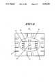
- FIG. 5is a top plan view of a glob top peripheral chip carrier in accordance with the present invention.
- FIG. 6is an exploded peripheral view of a glob top pad array carrier in accordance with the present invention.
- the chip carrieris an overmolded pad array carrier, an overmolded pin grid array, an overmolded peripheral chip carrier, or alternatively, a glob top pad array carrier, a glob top pin grid array, or a glob top peripheral chip carrier.
- the present inventionis applicable to any printed circuit board chip carrier having integrated circuits and an encapsulant such as an over mold or glob top.
- a substrate 16 for receiving a semiconductor die 14has printed circuitry 22 on the substrate 16.
- a hole(s) or aperture(s) 18is arranged and constructed so as to reside below the semiconductor die 14.
- the hole 18is preferably small enough (less than a 30 mil diameter) not to alter the design of the solder connections on the bottom of the package.
- a die attach adhesive 20such as a bisphenol-epichlorhydrin based epoxy which is preferably filled with silver is applied in the die attach region.
- the adhesiveis preferably dispensed onto the substrate, although other means of applying the adhesive is within contemplation of the present invention.
- the adhesiveis cured by using heat.
- the hole 18is usually partially filled with the adhesive after curing. The partially filled hole prevents mechanical damage to the die back plane, but allows water vapor to be expunged during temperature excursions such as during reflow soldering.
- an overmolded compound 12is applied over the die and portions of the substrate 16 forming the overmolded peripheral chip carrier 10 shown in FIG. 1.
- This overmolded pad array carrier 30further includes solder pads 38 on the bottom portion of a substrate 36 for receiving a semiconductor die 34 that has printed circuitry (not shown).
- a hole(s) or aperture(s) 42is arranged and constructed so as to reside below the semiconductor die 34.
- the hole 42is preferably small enough (less than a 30 mil diameter) not to alter the design of a solder bumped pad array on the bottom of a package as shown.
- a die attach adhesive 40is applied either to the bottom of the die 34 or the top surface of the substrate 36.
- the adhesive 40is preferably dispensed or screened onto the substrate 36, although other means of applying the adhesive is within contemplation of the present invention.
- an overmolded compound 32is formed over the die and portions of the substrate 36.
- FIG. 3there is shown a cut view of an overmolded pin grid array (OMPGA) 50.
- the OMPGAis formed essentially as described above in FIG. 2, with the addition of pins 51 protruding from the bottom of the package.
- the OMPGA 50comprises a substrate 56 having at least one aperture 55 residing below a semiconductor die 54.
- the back plane of the die 54is attached to the substrate 56 via an adhesive 58.
- Some of the conductive runners 57 on the substrate 56are coupled to the die 54 via a wirebond 53.
- an overmold 52is formed above the substrate and die.
- FIG. 4there is shown a cut view of an glob top pin grid array 60.
- the device 60is formed essentially as described above in FIG. 2, with the addition of pins 61 protruding from the bottom of the package and a glob top instead of an overmold.
- the device 60comprises a substrate 66 having at least one aperture 65 residing below a semiconductor die 64.
- the back plane of the die 64is attached to the substrate 66 via an adhesive 58.
- Some of the conductive runners 67 on the substrate 66are coupled to the die 64 via a wirebond 63. Once the die is wirebonded, then an glob top 62 is formed above the substrate and die.
- FIG. 5there is shown a top plan view of an glob top peripheral chip carrier 70.
- the device 70is formed essentially as described above in FIG. 1, with a glob top instead of an overmold.
- the device 70comprises a substrate 76 having at least one aperture 75 residing below a semiconductor die 74.
- the back plane of the die 74is attached to the substrate 76 via an adhesive (not shown).
- Some of the conductive runners 77 on the substrate 76are coupled to the die 74 via a wirebond 73.
- a glob top 72is formed above the substrate and die.
- FIG. 6there is shown an exploded peripheral view of an glob top pad array carrier 80.
- the device 80is formed essentially as described above in FIG. 2, with a glob top instead of an overmold.
- the device 80comprises a substrate 86 having at least one aperture 85 residing below a semiconductor die 84.
- the substrate 86further comprises several solder pads 81 on the bottom surface of the substrate 86.
- the back plane of the die 84is attached to the substrate 86 via an adhesive 88. Once the die is wirebonded, then a glob top 82 is formed above the substrate and die.
Landscapes
- Engineering & Computer Science (AREA)
- Microelectronics & Electronic Packaging (AREA)
- Computer Hardware Design (AREA)
- Power Engineering (AREA)
- Physics & Mathematics (AREA)
- Condensed Matter Physics & Semiconductors (AREA)
- General Physics & Mathematics (AREA)
- Die Bonding (AREA)
- Investigating Or Analysing Biological Materials (AREA)
- Peptides Or Proteins (AREA)
Abstract
Description
Claims (12)
Priority Applications (1)
| Application Number | Priority Date | Filing Date | Title |
|---|---|---|---|
| US07/927,774US5296738A (en) | 1991-07-08 | 1992-08-10 | Moisture relief for chip carrier |
Applications Claiming Priority (2)
| Application Number | Priority Date | Filing Date | Title |
|---|---|---|---|
| US72666091A | 1991-07-08 | 1991-07-08 | |
| US07/927,774US5296738A (en) | 1991-07-08 | 1992-08-10 | Moisture relief for chip carrier |
Related Parent Applications (1)
| Application Number | Title | Priority Date | Filing Date |
|---|---|---|---|
| US72666091AContinuation | 1991-07-08 | 1991-07-08 |
Publications (1)
| Publication Number | Publication Date |
|---|---|
| US5296738Atrue US5296738A (en) | 1994-03-22 |
Family
ID=24919498
Family Applications (1)
| Application Number | Title | Priority Date | Filing Date |
|---|---|---|---|
| US07/927,774Expired - LifetimeUS5296738A (en) | 1991-07-08 | 1992-08-10 | Moisture relief for chip carrier |
Country Status (5)
| Country | Link |
|---|---|
| US (1) | US5296738A (en) |
| EP (1) | EP0603198A4 (en) |
| JP (1) | JPH07500947A (en) |
| KR (1) | KR0134902B1 (en) |
| WO (1) | WO1993001619A1 (en) |
Cited By (33)
| Publication number | Priority date | Publication date | Assignee | Title |
|---|---|---|---|---|
| US5525834A (en)* | 1994-10-17 | 1996-06-11 | W. L. Gore & Associates, Inc. | Integrated circuit package |
| US5609889A (en)* | 1995-05-26 | 1997-03-11 | Hestia Technologies, Inc. | Apparatus for encapsulating electronic packages |
| US5652463A (en)* | 1995-05-26 | 1997-07-29 | Hestia Technologies, Inc. | Transfer modlded electronic package having a passage means |
| US5696666A (en)* | 1995-10-11 | 1997-12-09 | Motorola, Inc. | Low profile exposed die chip carrier package |
| US5701032A (en)* | 1994-10-17 | 1997-12-23 | W. L. Gore & Associates, Inc. | Integrated circuit package |
| US5710071A (en)* | 1995-12-04 | 1998-01-20 | Motorola, Inc. | Process for underfilling a flip-chip semiconductor device |
| US5721450A (en)* | 1995-06-12 | 1998-02-24 | Motorola, Inc. | Moisture relief for chip carriers |
| US5756380A (en)* | 1995-11-02 | 1998-05-26 | Motorola, Inc. | Method for making a moisture resistant semiconductor device having an organic substrate |
| US5894108A (en)* | 1997-02-11 | 1999-04-13 | National Semiconductor Corporation | Plastic package with exposed die |
| US5927505A (en)* | 1995-07-24 | 1999-07-27 | Lsi Logic Corporation | Overmolded package body on a substrate |
| US6014318A (en)* | 1997-10-27 | 2000-01-11 | Nec Corporation | Resin-sealed type ball grid array IC package and manufacturing method thereof |
| US6054755A (en)* | 1997-10-14 | 2000-04-25 | Sumitomo Metal (Smi) Electronics Devices Inc. | Semiconductor package with improved moisture vapor relief function and method of fabricating the same |
| EP0884778A3 (en)* | 1997-05-15 | 2000-05-31 | Nippon Telegraph and Telephone Corporation | Semiconductor chip and method of manufacturing the same |
| US6080932A (en)* | 1998-04-14 | 2000-06-27 | Tessera, Inc. | Semiconductor package assemblies with moisture vents |
| US6242802B1 (en) | 1995-07-17 | 2001-06-05 | Motorola, Inc. | Moisture enhanced ball grid array package |
| US6324069B1 (en)* | 1997-10-29 | 2001-11-27 | Hestia Technologies, Inc. | Chip package with molded underfill |
| US20020175399A1 (en)* | 2000-08-24 | 2002-11-28 | James Stephen L. | Packaged microelectronic devices with pressure release elements and methods for manufacturing and using such packaged microelectronic devices |
| US20020182776A1 (en)* | 1997-07-30 | 2002-12-05 | Atsushi Fujisawa | Method of manufacturing a resin encapsulated semiconductor device to provide a vent hole in a base substrate |
| US6495083B2 (en) | 1997-10-29 | 2002-12-17 | Hestia Technologies, Inc. | Method of underfilling an integrated circuit chip |
| US20030029633A1 (en)* | 2000-08-23 | 2003-02-13 | Ahmad Syed Sajid | Interconnecting substrates for electrical coupling of microelectronic components |
| US20030038357A1 (en)* | 2001-08-24 | 2003-02-27 | Derderian James M. | Spacer for semiconductor devices, semiconductor devices and assemblies including the spacer, and methods |
| US6653173B2 (en) | 2000-06-16 | 2003-11-25 | Micron Technology, Inc. | Method and apparatus for packaging a microelectronic die |
| US20040061127A1 (en)* | 2002-09-30 | 2004-04-01 | Xuejun Fan | Integrated circuit package including sealed gaps and prevention of vapor induced failures and method of manufacturing the same |
| US6803251B2 (en)* | 1998-02-10 | 2004-10-12 | Hyundai Electronics Industries Co., Ltd. | Integrated device package and fabrication methods thereof |
| US6838760B1 (en) | 2000-08-28 | 2005-01-04 | Micron Technology, Inc. | Packaged microelectronic devices with interconnecting units |
| US20050040514A1 (en)* | 2003-08-22 | 2005-02-24 | Samsung Electronics Co., Ltd. | Semiconductor package with improved chip attachment and manufacturing method thereof |
| US20050224936A1 (en)* | 2004-04-12 | 2005-10-13 | Jeng-Dah Wu | Chip package structure |
| US20060261498A1 (en)* | 2005-05-17 | 2006-11-23 | Micron Technology, Inc. | Methods and apparatuses for encapsulating microelectronic devices |
| US20080206930A1 (en)* | 2007-02-23 | 2008-08-28 | Micron Technology, Inc. | Systems and methods for compressing an encapsulant adjacent a semiconductor workpiece |
| US20110296680A1 (en)* | 2010-06-05 | 2011-12-08 | Raytheon Company | Vent blocking on vented ball grid arrays to provide a cleaner solution barrier |
| USRE43404E1 (en) | 1996-03-07 | 2012-05-22 | Tessera, Inc. | Methods for providing void-free layer for semiconductor assemblies |
| US9818703B2 (en)* | 2015-11-17 | 2017-11-14 | Samsung Electronics Co., Ltd. | Printed circuit board |
| US9914638B2 (en) | 2015-01-14 | 2018-03-13 | Sensirion Ag | Sensor package |
Families Citing this family (3)
| Publication number | Priority date | Publication date | Assignee | Title |
|---|---|---|---|---|
| KR100491494B1 (en)* | 1994-12-09 | 2005-08-25 | 소니 가부시끼 가이샤 | Semiconductor device |
| JP3414017B2 (en)* | 1994-12-09 | 2003-06-09 | ソニー株式会社 | Semiconductor device |
| WO1997035342A1 (en)* | 1996-03-22 | 1997-09-25 | The Whitaker Corporation | Printed wiring board substrate for chip on board device and process for fabrication thereof |
Citations (6)
| Publication number | Priority date | Publication date | Assignee | Title |
|---|---|---|---|---|
| US4329701A (en)* | 1978-03-20 | 1982-05-11 | The Trane Company | Semiconductor package |
| US4760440A (en)* | 1983-10-31 | 1988-07-26 | General Electric Company | Package for solid state image sensors |
| US4768081A (en)* | 1984-11-17 | 1988-08-30 | Messerschmitt-Boelkow-Blohm Gmbh | Process for encapsulating microelectronic circuits with organic components |
| US4866506A (en)* | 1984-04-02 | 1989-09-12 | Oki Electric Industry Co., Ltd. | Plastic-sealed IC device of heat-resistant construction |
| US4942452A (en)* | 1987-02-25 | 1990-07-17 | Hitachi, Ltd. | Lead frame and semiconductor device |
| JPH03178153A (en)* | 1989-12-07 | 1991-08-02 | Matsushita Electron Corp | Semiconductor device |
Family Cites Families (2)
| Publication number | Priority date | Publication date | Assignee | Title |
|---|---|---|---|---|
| US4483067A (en)* | 1981-09-11 | 1984-11-20 | U.S. Philips Corporation | Method of manufacturing an identification card and an identification manufactured, for example, by this method |
| GB8413330D0 (en)* | 1984-05-24 | 1984-06-27 | Mbm Technology Ltd | Mounting semi-conductor chips |
- 1992
- 1992-07-02WOPCT/US1992/005580patent/WO1993001619A1/ennot_activeApplication Discontinuation
- 1992-07-02JPJP5502327Apatent/JPH07500947A/enactivePending
- 1992-07-02KRKR1019940700055Apatent/KR0134902B1/ennot_activeExpired - Fee Related
- 1992-07-02EPEP9292915115Apatent/EP0603198A4/ennot_activeWithdrawn
- 1992-08-10USUS07/927,774patent/US5296738A/ennot_activeExpired - Lifetime
Patent Citations (6)
| Publication number | Priority date | Publication date | Assignee | Title |
|---|---|---|---|---|
| US4329701A (en)* | 1978-03-20 | 1982-05-11 | The Trane Company | Semiconductor package |
| US4760440A (en)* | 1983-10-31 | 1988-07-26 | General Electric Company | Package for solid state image sensors |
| US4866506A (en)* | 1984-04-02 | 1989-09-12 | Oki Electric Industry Co., Ltd. | Plastic-sealed IC device of heat-resistant construction |
| US4768081A (en)* | 1984-11-17 | 1988-08-30 | Messerschmitt-Boelkow-Blohm Gmbh | Process for encapsulating microelectronic circuits with organic components |
| US4942452A (en)* | 1987-02-25 | 1990-07-17 | Hitachi, Ltd. | Lead frame and semiconductor device |
| JPH03178153A (en)* | 1989-12-07 | 1991-08-02 | Matsushita Electron Corp | Semiconductor device |
Cited By (61)
| Publication number | Priority date | Publication date | Assignee | Title |
|---|---|---|---|---|
| US5525834A (en)* | 1994-10-17 | 1996-06-11 | W. L. Gore & Associates, Inc. | Integrated circuit package |
| US5701032A (en)* | 1994-10-17 | 1997-12-23 | W. L. Gore & Associates, Inc. | Integrated circuit package |
| US5652463A (en)* | 1995-05-26 | 1997-07-29 | Hestia Technologies, Inc. | Transfer modlded electronic package having a passage means |
| US5776512A (en)* | 1995-05-26 | 1998-07-07 | Hestia Technologies, Inc. | Apparatus for encapsulating electronic packages |
| US5609889A (en)* | 1995-05-26 | 1997-03-11 | Hestia Technologies, Inc. | Apparatus for encapsulating electronic packages |
| US5766986A (en)* | 1995-05-26 | 1998-06-16 | Hestia Technologies, Inc. | Method of transfer molding electronic packages and packages produced thereby |
| US5721450A (en)* | 1995-06-12 | 1998-02-24 | Motorola, Inc. | Moisture relief for chip carriers |
| US6242802B1 (en) | 1995-07-17 | 2001-06-05 | Motorola, Inc. | Moisture enhanced ball grid array package |
| US5927505A (en)* | 1995-07-24 | 1999-07-27 | Lsi Logic Corporation | Overmolded package body on a substrate |
| US5696666A (en)* | 1995-10-11 | 1997-12-09 | Motorola, Inc. | Low profile exposed die chip carrier package |
| US5756380A (en)* | 1995-11-02 | 1998-05-26 | Motorola, Inc. | Method for making a moisture resistant semiconductor device having an organic substrate |
| US5710071A (en)* | 1995-12-04 | 1998-01-20 | Motorola, Inc. | Process for underfilling a flip-chip semiconductor device |
| USRE43404E1 (en) | 1996-03-07 | 2012-05-22 | Tessera, Inc. | Methods for providing void-free layer for semiconductor assemblies |
| US5894108A (en)* | 1997-02-11 | 1999-04-13 | National Semiconductor Corporation | Plastic package with exposed die |
| US6117710A (en)* | 1997-02-11 | 2000-09-12 | National Semiconductor Corporation | Plastic package with exposed die and method of making same |
| EP0884778A3 (en)* | 1997-05-15 | 2000-05-31 | Nippon Telegraph and Telephone Corporation | Semiconductor chip and method of manufacturing the same |
| US6764878B2 (en)* | 1997-07-30 | 2004-07-20 | Renesas Technology Corp. | Method of manufacturing a resin encapsulated semiconductor device to provide a vent hole in a base substrate |
| US20020182776A1 (en)* | 1997-07-30 | 2002-12-05 | Atsushi Fujisawa | Method of manufacturing a resin encapsulated semiconductor device to provide a vent hole in a base substrate |
| US6054755A (en)* | 1997-10-14 | 2000-04-25 | Sumitomo Metal (Smi) Electronics Devices Inc. | Semiconductor package with improved moisture vapor relief function and method of fabricating the same |
| US6014318A (en)* | 1997-10-27 | 2000-01-11 | Nec Corporation | Resin-sealed type ball grid array IC package and manufacturing method thereof |
| US6324069B1 (en)* | 1997-10-29 | 2001-11-27 | Hestia Technologies, Inc. | Chip package with molded underfill |
| US6495083B2 (en) | 1997-10-29 | 2002-12-17 | Hestia Technologies, Inc. | Method of underfilling an integrated circuit chip |
| US6560122B2 (en) | 1997-10-29 | 2003-05-06 | Hestia Technologies, Inc. | Chip package with molded underfill |
| US6803251B2 (en)* | 1998-02-10 | 2004-10-12 | Hyundai Electronics Industries Co., Ltd. | Integrated device package and fabrication methods thereof |
| US6358780B1 (en) | 1998-04-14 | 2002-03-19 | Tessera, Inc. | Semiconductor package assemblies with moisture vents and methods of making same |
| US6080932A (en)* | 1998-04-14 | 2000-06-27 | Tessera, Inc. | Semiconductor package assemblies with moisture vents |
| US6664139B2 (en) | 2000-06-16 | 2003-12-16 | Micron Technology, Inc. | Method and apparatus for packaging a microelectronic die |
| US6677675B2 (en) | 2000-06-16 | 2004-01-13 | Micron Technology, Inc. | Microelectronic devices and microelectronic die packages |
| US6683388B2 (en) | 2000-06-16 | 2004-01-27 | Micron Technology, Inc. | Method and apparatus for packaging a microelectronic die |
| US6653173B2 (en) | 2000-06-16 | 2003-11-25 | Micron Technology, Inc. | Method and apparatus for packaging a microelectronic die |
| US20030029633A1 (en)* | 2000-08-23 | 2003-02-13 | Ahmad Syed Sajid | Interconnecting substrates for electrical coupling of microelectronic components |
| US6982386B2 (en) | 2000-08-23 | 2006-01-03 | Micron Technology, Inc. | Interconnecting substrates for electrical coupling of microelectronic components |
| US20030109083A1 (en)* | 2000-08-23 | 2003-06-12 | Ahmad Syed Sajid | Interconnecting substrates for electrical coupling of microelectronic components |
| US6983551B2 (en) | 2000-08-23 | 2006-01-10 | Micron Technology, Inc. | Interconnecting substrates for electrical coupling of microelectronic components |
| US6796028B2 (en) | 2000-08-23 | 2004-09-28 | Micron Technology, Inc. | Method of Interconnecting substrates for electrical coupling of microelectronic components |
| US20030106709A1 (en)* | 2000-08-23 | 2003-06-12 | Ahmad Syed Sajid | Interconnecting substrates for electrical coupling of microelectronic components |
| US7049685B2 (en) | 2000-08-24 | 2006-05-23 | Micron Technology, Inc. | Packaged microelectronic devices with pressure release elements and methods for manufacturing and using such packaged microelectronic devices |
| US6979595B1 (en)* | 2000-08-24 | 2005-12-27 | Micron Technology, Inc. | Packaged microelectronic devices with pressure release elements and methods for manufacturing and using such packaged microelectronic devices |
| US20060180907A1 (en)* | 2000-08-24 | 2006-08-17 | Micron Technology, Inc. | Packaged microelectronic devices with pressure release elements and methods for manufacturing and using such packaged microelectonic devices |
| US20020175399A1 (en)* | 2000-08-24 | 2002-11-28 | James Stephen L. | Packaged microelectronic devices with pressure release elements and methods for manufacturing and using such packaged microelectronic devices |
| US20070063335A1 (en)* | 2000-08-28 | 2007-03-22 | Micron Technology, Inc. | Packaged microelectronic devices with interconnecting units and methods for manufacturing and using the interconnecting units |
| US6838760B1 (en) | 2000-08-28 | 2005-01-04 | Micron Technology, Inc. | Packaged microelectronic devices with interconnecting units |
| US7101737B2 (en) | 2000-08-28 | 2006-09-05 | Micron Technology, Inc. | Method of encapsulating interconnecting units in packaged microelectronic devices |
| US20050056919A1 (en)* | 2000-08-28 | 2005-03-17 | Cobbley Chad A. | Packaged microelectronic devices with interconnecting units and methods for manufacturing and using the interconnecting units |
| US7332376B2 (en) | 2000-08-28 | 2008-02-19 | Micron Technology, Inc. | Method of encapsulating packaged microelectronic devices with a barrier |
| US7518223B2 (en) | 2001-08-24 | 2009-04-14 | Micron Technology, Inc. | Semiconductor devices and semiconductor device assemblies including a nonconfluent spacer layer |
| US20060035408A1 (en)* | 2001-08-24 | 2006-02-16 | Derderian James M | Methods for designing spacers for use in stacking semiconductor devices or semiconductor device components |
| US20030038355A1 (en)* | 2001-08-24 | 2003-02-27 | Derderian James M. | Semiconductor devices and semiconductor device assemblies including a nonconfluent spacer layer |
| US20030038357A1 (en)* | 2001-08-24 | 2003-02-27 | Derderian James M. | Spacer for semiconductor devices, semiconductor devices and assemblies including the spacer, and methods |
| US6773964B2 (en) | 2002-09-30 | 2004-08-10 | Koninklijke Philips Electronics N.V. | Integrated circuit package including sealed gaps and prevention of vapor induced failures and method of manufacturing the same |
| US20040061127A1 (en)* | 2002-09-30 | 2004-04-01 | Xuejun Fan | Integrated circuit package including sealed gaps and prevention of vapor induced failures and method of manufacturing the same |
| US7235887B2 (en)* | 2003-08-22 | 2007-06-26 | Samsung Electronics Co., Ltd. | Semiconductor package with improved chip attachment and manufacturing method thereof |
| US20050040514A1 (en)* | 2003-08-22 | 2005-02-24 | Samsung Electronics Co., Ltd. | Semiconductor package with improved chip attachment and manufacturing method thereof |
| US20050224936A1 (en)* | 2004-04-12 | 2005-10-13 | Jeng-Dah Wu | Chip package structure |
| US20060261498A1 (en)* | 2005-05-17 | 2006-11-23 | Micron Technology, Inc. | Methods and apparatuses for encapsulating microelectronic devices |
| US20080206930A1 (en)* | 2007-02-23 | 2008-08-28 | Micron Technology, Inc. | Systems and methods for compressing an encapsulant adjacent a semiconductor workpiece |
| US7833456B2 (en) | 2007-02-23 | 2010-11-16 | Micron Technology, Inc. | Systems and methods for compressing an encapsulant adjacent a semiconductor workpiece |
| US20110296680A1 (en)* | 2010-06-05 | 2011-12-08 | Raytheon Company | Vent blocking on vented ball grid arrays to provide a cleaner solution barrier |
| US8522426B2 (en)* | 2010-06-05 | 2013-09-03 | Raytheon Company | Vent blocking on vented ball grid arrays to provide a cleaner solution barrier |
| US9914638B2 (en) | 2015-01-14 | 2018-03-13 | Sensirion Ag | Sensor package |
| US9818703B2 (en)* | 2015-11-17 | 2017-11-14 | Samsung Electronics Co., Ltd. | Printed circuit board |
Also Published As
| Publication number | Publication date |
|---|---|
| EP0603198A1 (en) | 1994-06-29 |
| KR0134902B1 (en) | 1998-04-20 |
| EP0603198A4 (en) | 1994-08-17 |
| JPH07500947A (en) | 1995-01-26 |
| WO1993001619A1 (en) | 1993-01-21 |
Similar Documents
| Publication | Publication Date | Title |
|---|---|---|
| US5296738A (en) | Moisture relief for chip carrier | |
| US5721450A (en) | Moisture relief for chip carriers | |
| US5696666A (en) | Low profile exposed die chip carrier package | |
| US5241133A (en) | Leadless pad array chip carrier | |
| US6608388B2 (en) | Delamination-preventing substrate and semiconductor package with the same | |
| US6242802B1 (en) | Moisture enhanced ball grid array package | |
| US6323066B2 (en) | Heat-dissipating structure for integrated circuit package | |
| US6307257B1 (en) | Dual-chip integrated circuit package with a chip-die pad formed from leadframe leads | |
| US6964888B2 (en) | Semiconductor device and method for fabricating the same | |
| KR100192028B1 (en) | Plastic package type semiconductor device | |
| US6855575B2 (en) | Semiconductor chip package having a semiconductor chip with center and edge bonding pads and manufacturing method thereof | |
| US6028356A (en) | Plastic-packaged semiconductor integrated circuit | |
| US20020079570A1 (en) | Semiconductor package with heat dissipating element | |
| JP2822272B2 (en) | Leadless pad array chip carrier | |
| US20050046003A1 (en) | Stacked-chip semiconductor package and fabrication method thereof | |
| US5633206A (en) | Process for manufacturing lead frame for semiconductor package | |
| JPH11150213A (en) | Semiconductor device | |
| JP3655338B2 (en) | Resin-sealed semiconductor device and manufacturing method thereof | |
| JPH05160296A (en) | Resin sealing method of semiconductor integrated circuit bare chip | |
| KR0119757Y1 (en) | Semiconductor package | |
| KR200154510Y1 (en) | Lead on chip package | |
| JP3358697B2 (en) | Semiconductor package | |
| JP3732660B2 (en) | Resin-sealed semiconductor device | |
| KR940006578B1 (en) | Semiconductor package and manufacturing method | |
| US20020105095A1 (en) | Semiconductor package having a substrate including a die-attach aperture and method for packaging a semiconductor die |
Legal Events
| Date | Code | Title | Description |
|---|---|---|---|
| STCF | Information on status: patent grant | Free format text:PATENTED CASE | |
| FPAY | Fee payment | Year of fee payment:4 | |
| FPAY | Fee payment | Year of fee payment:8 | |
| AS | Assignment | Owner name:FREESCALE SEMICONDUCTOR, INC., TEXAS Free format text:ASSIGNMENT OF ASSIGNORS INTEREST;ASSIGNOR:MOTOROLA, INC.;REEL/FRAME:015698/0657 Effective date:20040404 Owner name:FREESCALE SEMICONDUCTOR, INC.,TEXAS Free format text:ASSIGNMENT OF ASSIGNORS INTEREST;ASSIGNOR:MOTOROLA, INC.;REEL/FRAME:015698/0657 Effective date:20040404 | |
| FPAY | Fee payment | Year of fee payment:12 | |
| AS | Assignment | Owner name:CITIBANK, N.A. AS COLLATERAL AGENT, NEW YORK Free format text:SECURITY AGREEMENT;ASSIGNORS:FREESCALE SEMICONDUCTOR, INC.;FREESCALE ACQUISITION CORPORATION;FREESCALE ACQUISITION HOLDINGS CORP.;AND OTHERS;REEL/FRAME:018855/0129 Effective date:20061201 Owner name:CITIBANK, N.A. AS COLLATERAL AGENT,NEW YORK Free format text:SECURITY AGREEMENT;ASSIGNORS:FREESCALE SEMICONDUCTOR, INC.;FREESCALE ACQUISITION CORPORATION;FREESCALE ACQUISITION HOLDINGS CORP.;AND OTHERS;REEL/FRAME:018855/0129 Effective date:20061201 | |
| AS | Assignment | Owner name:CITIBANK, N.A., AS COLLATERAL AGENT,NEW YORK Free format text:SECURITY AGREEMENT;ASSIGNOR:FREESCALE SEMICONDUCTOR, INC.;REEL/FRAME:024397/0001 Effective date:20100413 Owner name:CITIBANK, N.A., AS COLLATERAL AGENT, NEW YORK Free format text:SECURITY AGREEMENT;ASSIGNOR:FREESCALE SEMICONDUCTOR, INC.;REEL/FRAME:024397/0001 Effective date:20100413 | |
| AS | Assignment | Owner name:FREESCALE SEMICONDUCTOR, INC., TEXAS Free format text:PATENT RELEASE;ASSIGNOR:CITIBANK, N.A., AS COLLATERAL AGENT;REEL/FRAME:037354/0225 Effective date:20151207 Owner name:FREESCALE SEMICONDUCTOR, INC., TEXAS Free format text:PATENT RELEASE;ASSIGNOR:CITIBANK, N.A., AS COLLATERAL AGENT;REEL/FRAME:037356/0553 Effective date:20151207 Owner name:FREESCALE SEMICONDUCTOR, INC., TEXAS Free format text:PATENT RELEASE;ASSIGNOR:CITIBANK, N.A., AS COLLATERAL AGENT;REEL/FRAME:037356/0143 Effective date:20151207 |