US5296721A - Strained interband resonant tunneling negative resistance diode - Google Patents
Strained interband resonant tunneling negative resistance diodeDownload PDFInfo
- Publication number
- US5296721A US5296721AUS07/923,397US92339792AUS5296721AUS 5296721 AUS5296721 AUS 5296721AUS 92339792 AUS92339792 AUS 92339792AUS 5296721 AUS5296721 AUS 5296721A
- Authority
- US
- United States
- Prior art keywords
- quantum well
- barrier
- electron injection
- tunnel diode
- energy
- Prior art date
- Legal status (The legal status is an assumption and is not a legal conclusion. Google has not performed a legal analysis and makes no representation as to the accuracy of the status listed.)
- Expired - Lifetime
Links
Images
Classifications
- B—PERFORMING OPERATIONS; TRANSPORTING
- B82—NANOTECHNOLOGY
- B82Y—SPECIFIC USES OR APPLICATIONS OF NANOSTRUCTURES; MEASUREMENT OR ANALYSIS OF NANOSTRUCTURES; MANUFACTURE OR TREATMENT OF NANOSTRUCTURES
- B82Y10/00—Nanotechnology for information processing, storage or transmission, e.g. quantum computing or single electron logic
- H—ELECTRICITY
- H10—SEMICONDUCTOR DEVICES; ELECTRIC SOLID-STATE DEVICES NOT OTHERWISE PROVIDED FOR
- H10D—INORGANIC ELECTRIC SEMICONDUCTOR DEVICES
- H10D62/00—Semiconductor bodies, or regions thereof, of devices having potential barriers
- H10D62/80—Semiconductor bodies, or regions thereof, of devices having potential barriers characterised by the materials
- H10D62/81—Semiconductor bodies, or regions thereof, of devices having potential barriers characterised by the materials of structures exhibiting quantum-confinement effects, e.g. single quantum wells; of structures having periodic or quasi-periodic potential variation
- H10D62/812—Single quantum well structures
- H—ELECTRICITY
- H10—SEMICONDUCTOR DEVICES; ELECTRIC SOLID-STATE DEVICES NOT OTHERWISE PROVIDED FOR
- H10D—INORGANIC ELECTRIC SEMICONDUCTOR DEVICES
- H10D8/00—Diodes
- H10D8/70—Tunnel-effect diodes
- H10D8/755—Resonant tunneling diodes [RTD]
Definitions
- This inventionrelates to semiconductor diodes, and, more particularly, to a modified double barrier tunnel diode.
- a diodeis a semiconductor device having a nonlinear voltage-current relation. Diodes are among the most important of solid-state devices, and are used in many electronic applications.
- the tunnel diodeis one variety of diode, having the unusual characteristic of negative resistance. As the term is used, negative resistance is a voltage-current behavior wherein, over certain voltage ranges, increasing the voltage applied across the diode leads to decreased current carried through the diode. By contrast, in most devices an increasing applied voltage results in increasing current. Tunnel diodes have a number of applications, including high frequency oscillator circuits and high frequency electronic switches.
- One type of tunnel diodeis the double barrier tunnel diode.
- One such double barrier tunnel diodeincludes a gallium antimonide quantum well with a thin barrier layer of aluminum antimonide epitaxially joined to each side of the quantum well.
- This structuretermed a quantum barrier, in turn lies between two injection layers of indium arsenide.
- the quantum barriercreates an energy barrier to the flow of electrons that can be overcome by electrons only under certain conditions, and which results in the negative resistance characteristic of interest over a range of applied bias voltage. Electrons are injected into the quantum barrier from the conduction band of one of the injection layers under an internal voltage, produced by the applied external voltage. The internal voltage increases the energy of the injected electrons to satisfy the resonant tunneling condition of the quantum barrier.
- the incoming electronhas the same energy as a valence level of the quantum well, and the electrons tunnel through the quantum barrier.
- the bias voltageis increased further, the energy levels no longer align and the current decreases, resulting in the negative resistance effect.
- the magnitude of the negative resistance effectis not as great as might be expected. It is important to understand the cause of this reduced negative-resistance effect, and an associated need for an improved double barrier tunnel diode that exhibits the full extent of the negative-resistance effect.
- the present inventionfulfills this need, and further provides related advantages.
- the present inventionprovides an improved double barrier tunnel diode. This diode avoids the reduced magnitude of the negative-resistance effect observed in some other similar diodes. It is structurally similar to conventional diodes, and can be substituted for conventional diodes.
- a double barrier tunnel diodecomprises a quantum well having at least one layer of a semiconductor material.
- a pair of electron injection layersare disposed on either side of the quantum well, and a barrier layer is positioned between each of the electron injection layers and the quantum well.
- the barrier layershave a thickness sufficiently small to permit electrons to tunnel through the barriers and the quantum well.
- the barrier layersfurther have a biaxially strained epitaxial relationship with the material of the quantum well, the biaxial stress and strain being sufficient to reduce the energy of heavy holes in the quantum well to less than the energy of the conduction band minimum energy of the electron injection layers.
- the quantum wellis less than about 200 Angstroms thick and is made of gallium antimonide with from about 1 to about 40 atomic percent arsenic therein.
- the electron injection layersare made of indium arsenide.
- the barrier layersare each less than about 40 Angstroms thick and are made of aluminum antimonide. The application of the invention is not limited to this structure, however.
- the arsenic additiondecreases the lattice constant of the gallium antimonide of the quantum well.
- the arsenic additionis limited to an amount that will not cause the loss of coherency and the epitaxial interfacial structure, with the result that the quantum well is placed into biaxial tension. This tensile stress splits the energy levels of the heavy and light holes in the quantum well, and decreases the energy level of the heavy holes relative to the light holes. With a sufficient addition of the alloying element into the material of the quantum well, the energy level of the heavy holes is decreased sufficiently that it is below the conduction energy level of the injection layer.
- the heavy holesdo not enter into the quantum tunneling effect because a bias voltage raises the energy of the injected electrons even further above the energy of the heavy holes.
- the light holescan contribute to the negative resistance effect, the desired result. It has been found that the heavy holes provide a competing channel for conduction to the desired light holes, and therefore the elimination of the heavy holes from the conduction process results in improved negative resistance performance of the diode.
- the present diodeis more effective than the conventional comparable diode in achieving a negative resistance effect.
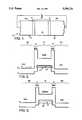
- FIG. 1is a schematic sectional view of a double barrier tunnel diode
- FIG. 2is a schematic diagram of the structure of FIG. 1, with an indication of energy states in the conventional diode;
- FIG. 3is a schematic diagram of the structure of FIG. 1, with an indication of energy states in the diode of the invention.
- the present inventionis embodied in a double barrier tunnel diode 10, illustrated in FIG. 1.
- a tunnel diode 10includes a quantum well 12, bounded on each side by a barrier layer 14.
- the quantum well 12 and the two barrier layers 14are together termed herein a quantum barrier 15.
- the diode 10is prepared by depositing these layers sequentially.
- injection layer 16aIn operation, electrons are supplied from one of the injection layers, here illustrated as injection layer 16a. Under the application of an external biasing voltage V b , electrons from the injection layer 16a resonantly tunnel through the quantum barrier 15 to the other injection layer 16b. The result is a current through the quantum barrier 15 and the diode 10.
- the quantum wellis single crystal gallium antimonide (GaSb) of a thickness of less than about 200 Angstroms.
- the barrier layers 14are single crystal aluminum antimonide (AlSb), each of a thickness of less than about 40 Angstroms.
- the injection layers 16are single crystal indium arsenide. Other materials are used in such diodes, and the present invention is not limited to this composition.
- the barrier layers 14are in epitaxial relation to the quantum well 12, and the injection layers 16 are in epitaxial relation to the barrier layers 14.
- An "epitaxial" relationis one wherein the adjacent layers or structures have the same crystal structure and are crystallographically continuous between the two layers or structures. That the crystal structures are the same and continuous between the layers does not, however, imply that the lattice parameters of the two layers or structures are identical. In most cases, the lattice parameters are slightly mismatched, leading to a biaxial strain condition.
- the present inventiondoes not attempt to reduce the biaxial strain, but takes the opposite approach of increasing the biaxial strain to control to advantage the electron energy state of the quantum well.
- Biaxial strainis present when there is strain in two orthogonal directions in a material. Such biaxial strain often arises in other contexts when two materials with different lattice constants or coefficients of expansion are joined at an interface, so that stresses and strains are produced in each material in orthogonal directions parallel to the interface.
- FIG. 2depicts the relevant electron energy states for the diode of FIG. 1.
- the line indicated “E”represents the lowest electron energy states for the conduction band of each layer.
- the line indicated “E”represents the electron energy states for the valence band of each layer.
- Conduction through the diode 10occurs when conduction band electrons injected from the injection layer 16a (under the influence of the bias voltage V of FIG. 1) tunnel through the barrier layer 14, are conducted through the quantum well 12 in the valence band, tunnel through the other barrier layer 14, and enter the conduction band of the injection layer 16b.
- the heavy holes and light holeshave their own respective valence energy states, termed “HH” and “LH” in FIG. 2.
- the light hole resonanceis desired for tunneling, because it has a strong transmission probability and resulting high current densities. Because of the symmetry mismatch between it and the incoming electron state, the heavy hole resonance does not transmit as well as does the light hole resonance. The presence of the heavy hole resonance is undesirable because it provides an alternate channel for transport which tends to degrade the negative resistance effect.
- the heavy holeis always at a higher energy than the light hole resonance for this type of structure. Consequently, the application of a voltage V b will always result in interference from the heavy hole state as the device passes into the negative resistance region of its operation.
- a key feature of the present inventionis modifying the structure of the quantum well 12 to define the heavy hole energy state by splitting it from the light hole energy state.
- the heavy hole energy stateis reduced to a level below that of the conduction band of the injection layer 16a and thence below the energy of the injected electrons from the injection layer 16a. This modification must be achieved while maintaining the epitaxial relationship between the barrier layer 14 and the quantum well layer 12.
- the quantum well layer 12is alloyed by the addition of an alloying element so that its lattice parameter is decreased.
- the decrease in the lattice parameter of the quantum wellresults in the creation of biaxial tensile stresses and strains in the quantum well layer 12.
- the epitaxial relationship with the barrier layer 14 and the lattice parameter of the barrier layer 14remain unchanged.
- the compressive stress and strain state in the quantum well layer 12selectively reduces the energy level of the heavy holes, as shown in FIG. 3.
- a sufficient addition of the alloying elementis made to the quantum well material to increase the biaxial tensile stress and strain by an amount such that the energy level of the heavy holes is reduced below the minimum conduction band energy of the injection layer.
- the heavy holesdo not contribute to the resonant tunneling through the quantum barrier, and therefore do not affect the negative resistance region achieved when the voltage V b is further increased. Consequently, the modified diode exhibits an enhanced negative resistance effect as compared with the unmodified conventional diode.
- the quantum well layeris modified by adding an element that decreases its lattice constant.
- the preferred alloying elementis arsenic.
- Arsenicis incorporated into the material of the quantum well during its growth, as by molecular beam epitaxy.
- the amount of arsenic addedcan vary over a limited range.
- the amount of arsenicmust be sufficient to reduce the energy level of the heavy holes to below that of the conduction band of the injection layer, here indium arsenide.
- the minimum operable amount of arsenicis estimated to be about 1 atomic percent.
- the tensile strainincreases so that, at some point, the system energy can be reduced by nucleating a defect and the epitaxial relationship is lost.
- the amount of arsenic added to the gallium antimonide of the quantum wellmust not be so great that the epitaxial relationship between the aluminum antimonide barrier layer 14 and the quantum well 12 is lost.
- the maximum amount of arsenic that may be added to the gallium antimonide of the quantum wellis estimated to be about 40 atomic percent, although the exact value may depend upon the thickness of the quantum well.
- the arsenicshould remain within the range of from about 1 to about 40 atomic percent.
- similar physical principlesapply, but the numerical values will vary.
- the present inventionprovides a double barrier tunnel diode of improved structure and operation in achieving the important negative resistance function.
Landscapes
- Engineering & Computer Science (AREA)
- Chemical & Material Sciences (AREA)
- Nanotechnology (AREA)
- Physics & Mathematics (AREA)
- Mathematical Physics (AREA)
- Theoretical Computer Science (AREA)
- Crystallography & Structural Chemistry (AREA)
- Bipolar Transistors (AREA)
Abstract
Description
Claims (13)
Priority Applications (4)
| Application Number | Priority Date | Filing Date | Title |
|---|---|---|---|
| US07/923,397US5296721A (en) | 1992-07-31 | 1992-07-31 | Strained interband resonant tunneling negative resistance diode |
| IL106496AIL106496A0 (en) | 1992-07-31 | 1993-07-27 | Strained interband resonant tunneling negative resistance diode |
| EP9393111977AEP0581239A3 (en) | 1992-07-31 | 1993-07-28 | Strained interband resonant tunneling negative resistance diode |
| JP5191450AJPH06188437A (en) | 1992-07-31 | 1993-08-02 | Distorted in-band resonant tunneling negative resistance diode |
Applications Claiming Priority (1)
| Application Number | Priority Date | Filing Date | Title |
|---|---|---|---|
| US07/923,397US5296721A (en) | 1992-07-31 | 1992-07-31 | Strained interband resonant tunneling negative resistance diode |
Publications (1)
| Publication Number | Publication Date |
|---|---|
| US5296721Atrue US5296721A (en) | 1994-03-22 |
Family
ID=25448633
Family Applications (1)
| Application Number | Title | Priority Date | Filing Date |
|---|---|---|---|
| US07/923,397Expired - LifetimeUS5296721A (en) | 1992-07-31 | 1992-07-31 | Strained interband resonant tunneling negative resistance diode |
Country Status (4)
| Country | Link |
|---|---|
| US (1) | US5296721A (en) |
| EP (1) | EP0581239A3 (en) |
| JP (1) | JPH06188437A (en) |
| IL (1) | IL106496A0 (en) |
Cited By (8)
| Publication number | Priority date | Publication date | Assignee | Title |
|---|---|---|---|---|
| US5436469A (en)* | 1994-06-15 | 1995-07-25 | Moll; Nicolas J. | Band minima transistor |
| US5488507A (en)* | 1993-10-04 | 1996-01-30 | Canon Kabushiki Kaisha | Semiconductor optical amplifier having reduced polarization dependence |
| US5497012A (en)* | 1994-06-15 | 1996-03-05 | Hewlett-Packard Company | Unipolar band minima devices |
| US5561301A (en)* | 1994-02-21 | 1996-10-01 | Fujitsu Limited | Opto-semiconductor device with piezoelectric |
| US5659180A (en)* | 1995-11-13 | 1997-08-19 | Motorola | Heterojunction interband tunnel diodes with improved P/V current ratios |
| US6320212B1 (en) | 1999-09-02 | 2001-11-20 | Hrl Laboratories, Llc. | Superlattice fabrication for InAs/GaSb/AISb semiconductor structures |
| WO2010091042A1 (en)* | 2009-02-03 | 2010-08-12 | Georgia State University Research Foundation, Inc. | High operating temperature split-off band infrared detector with double and/or graded barrier |
| US10615574B2 (en)* | 2018-05-17 | 2020-04-07 | Wisconsin Alumni Research Foundation | Superlattice heterostructures formed with single crystalline semiconductor nanomembranes and amorphous tunneling barrier layers |
Families Citing this family (34)
| Publication number | Priority date | Publication date | Assignee | Title |
|---|---|---|---|---|
| US6392257B1 (en) | 2000-02-10 | 2002-05-21 | Motorola Inc. | Semiconductor structure, semiconductor device, communicating device, integrated circuit, and process for fabricating the same |
| US6693033B2 (en) | 2000-02-10 | 2004-02-17 | Motorola, Inc. | Method of removing an amorphous oxide from a monocrystalline surface |
| JP2004503920A (en) | 2000-05-31 | 2004-02-05 | モトローラ・インコーポレイテッド | Semiconductor device and method of manufacturing the semiconductor device |
| US6501973B1 (en) | 2000-06-30 | 2002-12-31 | Motorola, Inc. | Apparatus and method for measuring selected physical condition of an animate subject |
| US6590236B1 (en) | 2000-07-24 | 2003-07-08 | Motorola, Inc. | Semiconductor structure for use with high-frequency signals |
| WO2002009187A2 (en)* | 2000-07-24 | 2002-01-31 | Motorola, Inc. | Heterojunction tunneling diodes and process for fabricating same |
| US6555946B1 (en) | 2000-07-24 | 2003-04-29 | Motorola, Inc. | Acoustic wave device and process for forming the same |
| US6493497B1 (en) | 2000-09-26 | 2002-12-10 | Motorola, Inc. | Electro-optic structure and process for fabricating same |
| US6638838B1 (en) | 2000-10-02 | 2003-10-28 | Motorola, Inc. | Semiconductor structure including a partially annealed layer and method of forming the same |
| US6501121B1 (en) | 2000-11-15 | 2002-12-31 | Motorola, Inc. | Semiconductor structure |
| US6583034B2 (en) | 2000-11-22 | 2003-06-24 | Motorola, Inc. | Semiconductor structure including a compliant substrate having a graded monocrystalline layer and methods for fabricating the structure and semiconductor devices including the structure |
| US6559471B2 (en) | 2000-12-08 | 2003-05-06 | Motorola, Inc. | Quantum well infrared photodetector and method for fabricating same |
| US20020096683A1 (en) | 2001-01-19 | 2002-07-25 | Motorola, Inc. | Structure and method for fabricating GaN devices utilizing the formation of a compliant substrate |
| US6673646B2 (en) | 2001-02-28 | 2004-01-06 | Motorola, Inc. | Growth of compound semiconductor structures on patterned oxide films and process for fabricating same |
| WO2002082551A1 (en) | 2001-04-02 | 2002-10-17 | Motorola, Inc. | A semiconductor structure exhibiting reduced leakage current |
| US6709989B2 (en) | 2001-06-21 | 2004-03-23 | Motorola, Inc. | Method for fabricating a semiconductor structure including a metal oxide interface with silicon |
| US6992321B2 (en) | 2001-07-13 | 2006-01-31 | Motorola, Inc. | Structure and method for fabricating semiconductor structures and devices utilizing piezoelectric materials |
| US6531740B2 (en) | 2001-07-17 | 2003-03-11 | Motorola, Inc. | Integrated impedance matching and stability network |
| US6646293B2 (en) | 2001-07-18 | 2003-11-11 | Motorola, Inc. | Structure for fabricating high electron mobility transistors utilizing the formation of complaint substrates |
| US6498358B1 (en) | 2001-07-20 | 2002-12-24 | Motorola, Inc. | Structure and method for fabricating an electro-optic system having an electrochromic diffraction grating |
| US7019332B2 (en) | 2001-07-20 | 2006-03-28 | Freescale Semiconductor, Inc. | Fabrication of a wavelength locker within a semiconductor structure |
| US6693298B2 (en) | 2001-07-20 | 2004-02-17 | Motorola, Inc. | Structure and method for fabricating epitaxial semiconductor on insulator (SOI) structures and devices utilizing the formation of a compliant substrate for materials used to form same |
| US6855992B2 (en) | 2001-07-24 | 2005-02-15 | Motorola Inc. | Structure and method for fabricating configurable transistor devices utilizing the formation of a compliant substrate for materials used to form the same |
| US6667196B2 (en) | 2001-07-25 | 2003-12-23 | Motorola, Inc. | Method for real-time monitoring and controlling perovskite oxide film growth and semiconductor structure formed using the method |
| US6639249B2 (en) | 2001-08-06 | 2003-10-28 | Motorola, Inc. | Structure and method for fabrication for a solid-state lighting device |
| US6589856B2 (en) | 2001-08-06 | 2003-07-08 | Motorola, Inc. | Method and apparatus for controlling anti-phase domains in semiconductor structures and devices |
| US20030034491A1 (en) | 2001-08-14 | 2003-02-20 | Motorola, Inc. | Structure and method for fabricating semiconductor structures and devices for detecting an object |
| US6673667B2 (en) | 2001-08-15 | 2004-01-06 | Motorola, Inc. | Method for manufacturing a substantially integral monolithic apparatus including a plurality of semiconductor materials |
| US20030071327A1 (en) | 2001-10-17 | 2003-04-17 | Motorola, Inc. | Method and apparatus utilizing monocrystalline insulator |
| US6916717B2 (en) | 2002-05-03 | 2005-07-12 | Motorola, Inc. | Method for growing a monocrystalline oxide layer and for fabricating a semiconductor device on a monocrystalline substrate |
| US7169619B2 (en) | 2002-11-19 | 2007-01-30 | Freescale Semiconductor, Inc. | Method for fabricating semiconductor structures on vicinal substrates using a low temperature, low pressure, alkaline earth metal-rich process |
| US6885065B2 (en) | 2002-11-20 | 2005-04-26 | Freescale Semiconductor, Inc. | Ferromagnetic semiconductor structure and method for forming the same |
| US6965128B2 (en) | 2003-02-03 | 2005-11-15 | Freescale Semiconductor, Inc. | Structure and method for fabricating semiconductor microresonator devices |
| US7020374B2 (en) | 2003-02-03 | 2006-03-28 | Freescale Semiconductor, Inc. | Optical waveguide structure and method for fabricating the same |
Citations (10)
| Publication number | Priority date | Publication date | Assignee | Title |
|---|---|---|---|---|
| US4286275A (en)* | 1980-02-04 | 1981-08-25 | International Business Machines Corporation | Semiconductor device |
| US4439782A (en)* | 1980-11-21 | 1984-03-27 | University Of Illinois Foundation | Semiconductor device with heterojunction of Alx Ga1-x As--AlAs--Ga |
| JPS5967676A (en)* | 1982-10-12 | 1984-04-17 | Nec Corp | Superlattice negative resistance element |
| JPS5990978A (en)* | 1982-11-16 | 1984-05-25 | Nec Corp | Superlattice negative resistance element |
| EP0081007B1 (en)* | 1981-12-09 | 1986-08-20 | International Business Machines Corporation | Superconducting tunnel junction device |
| US4780749A (en)* | 1986-07-01 | 1988-10-25 | Hughes Aircraft Company | Double barrier tunnel diode having modified injection layer |
| JPH01171280A (en)* | 1987-12-25 | 1989-07-06 | Fujitsu Ltd | Resonance tunnel barrier element |
| US5113231A (en)* | 1989-09-07 | 1992-05-12 | California Institute Of Technology | Quantum-effect semiconductor devices |
| US5132746A (en)* | 1991-01-04 | 1992-07-21 | International Business Machines Corporation | Biaxial-stress barrier shifts in pseudomorphic tunnel devices |
| JPH06184872A (en)* | 1991-09-11 | 1994-07-05 | Lamiflex Spa | Lightweight heald support frame for loom and centering device for side members thereof |
Family Cites Families (2)
| Publication number | Priority date | Publication date | Assignee | Title |
|---|---|---|---|---|
| JPS63276277A (en)* | 1987-05-08 | 1988-11-14 | Fujitsu Ltd | Semiconductor negative differential resistance element |
| JPH01241870A (en)* | 1988-03-23 | 1989-09-26 | Nec Corp | Resonance tunnel element |
- 1992
- 1992-07-31USUS07/923,397patent/US5296721A/ennot_activeExpired - Lifetime
- 1993
- 1993-07-27ILIL106496Apatent/IL106496A0/enunknown
- 1993-07-28EPEP9393111977Apatent/EP0581239A3/ennot_activeWithdrawn
- 1993-08-02JPJP5191450Apatent/JPH06188437A/enactivePending
Patent Citations (10)
| Publication number | Priority date | Publication date | Assignee | Title |
|---|---|---|---|---|
| US4286275A (en)* | 1980-02-04 | 1981-08-25 | International Business Machines Corporation | Semiconductor device |
| US4439782A (en)* | 1980-11-21 | 1984-03-27 | University Of Illinois Foundation | Semiconductor device with heterojunction of Alx Ga1-x As--AlAs--Ga |
| EP0081007B1 (en)* | 1981-12-09 | 1986-08-20 | International Business Machines Corporation | Superconducting tunnel junction device |
| JPS5967676A (en)* | 1982-10-12 | 1984-04-17 | Nec Corp | Superlattice negative resistance element |
| JPS5990978A (en)* | 1982-11-16 | 1984-05-25 | Nec Corp | Superlattice negative resistance element |
| US4780749A (en)* | 1986-07-01 | 1988-10-25 | Hughes Aircraft Company | Double barrier tunnel diode having modified injection layer |
| JPH01171280A (en)* | 1987-12-25 | 1989-07-06 | Fujitsu Ltd | Resonance tunnel barrier element |
| US5113231A (en)* | 1989-09-07 | 1992-05-12 | California Institute Of Technology | Quantum-effect semiconductor devices |
| US5132746A (en)* | 1991-01-04 | 1992-07-21 | International Business Machines Corporation | Biaxial-stress barrier shifts in pseudomorphic tunnel devices |
| JPH06184872A (en)* | 1991-09-11 | 1994-07-05 | Lamiflex Spa | Lightweight heald support frame for loom and centering device for side members thereof |
Non-Patent Citations (22)
| Title |
|---|
| D. Z. Y. Ting et al., Role of Heavy Hole States in interband tunnel structures , Appl. Phys. Lett. 58(3) Jan. 21, 1991, pp. 292 294.* |
| D. Z.-Y. Ting et al., "Role of Heavy-Hole States in interband tunnel structures", Appl. Phys. Lett. 58(3) Jan. 21, 1991, pp. 292-294. |
| J. R. Soderstrom et al., "New Negative Differential Resistance Device Based On Resonant Interband Tunneling," Appl. Phys. Lett. 55(11), Sep. 11, 1989, pp. 1094-1096. |
| J. R. Soderstrom et al., New Negative Differential Resistance Device Based On Resonant Interband Tunneling, Appl. Phys. Lett. 55(11), Sep. 11, 1989, pp. 1094 1096.* |
| J. Vac. Sci. Technol. B 8(4), Jul./Aug. 1990, "InAs/Ga1-x Inx Sb strained-layer superlattices grown by molecular-beam epitaxy", pp. 710-714, D. Chow et al. |
| J. Vac. Sci. Technol. B 8(4), Jul./Aug. 1990, InAs/Ga 1 x In x Sb strained layer superlattices grown by molecular beam epitaxy , pp. 710 714, D. Chow et al.* |
| Kaede et al., "High Speed GaAs/AlGaAs Photoconductive Detector Using a P-Modulation-Doped Multi Quantum Well Structure", Appl. Phys. Lett., 48(16), Apr. 21, 1986, pp. 1096-1097. |
| Kaede et al., High Speed GaAs/AlGaAs Photoconductive Detector Using a P Modulation Doped Multi Quantum Well Structure , Appl. Phys. Lett., 48(16), Apr. 21, 1986, pp. 1096 1097.* |
| M. S. Kiledjian et al., "Hole and interband resonant tunneling in GaAs/GaAlAs and InAs/GaSb/AlSb tunnel structures", Surface Science, North-Holland, vol. 267, 1992, pp. 405-408. |
| M. S. Kiledjian et al., Hole and interband resonant tunneling in GaAs/GaAlAs and InAs/GaSb/AlSb tunnel structures , Surface Science, North Holland, vol. 267, 1992, pp. 405 408.* |
| Neikirk et al, "Quantum-well devices will challenge HEMTs", Microwaves & RF, Jul. 1986, pp. 93-97. |
| Neikirk et al, Quantum well devices will challenge HEMTs , Microwaves & RF, Jul. 1986, pp. 93 97.* |
| Ray et al., "Resonant Tunneling Transport At 300K in GaAs-AlGaAs Quantum Wells Grown by Metallorganic Chemical Vapor Deposition", Appl. Phys. Lett., 48(24), Jun. 16, 1986, pp. 1666-1668. |
| Ray et al., Resonant Tunneling Transport At 300K in GaAs AlGaAs Quantum Wells Grown by Metallorganic Chemical Vapor Deposition , Appl. Phys. Lett., 48(24), Jun. 16, 1986, pp. 1666 1668.* |
| Shen et al., "Photoreflectance Study of GaAs/AlAs Superlattices: Fit to Electromodulation Theory", 48 Appl. Phys. Lett., Mar. 1986, pp. 653-655. |
| Shen et al., Photoreflectance Study of GaAs/AlAs Superlattices: Fit to Electromodulation Theory , 48 Appl. Phys. Lett., Mar. 1986, pp. 653 655.* |
| Sollner et al., "Resonant Tunneling through quantum wells at frequencies up to 2.5 THz", 43 Appl Phys. Lett., Sep. 1983, pp. 585-590. |
| Sollner et al., Resonant Tunneling through quantum wells at frequencies up to 2.5 THz , 43 Appl Phys. Lett., Sep. 1983, pp. 585 590.* |
| Summers et al., "Variably Spaced Superlattice Energy Filter, A New Device Design Concept for High-Energy Electron Injection," Appl. Phys. Lett., 48(12) Mar. 24, 1986, pp. 806-808. |
| Summers et al., Variably Spaced Superlattice Energy Filter, A New Device Design Concept for High Energy Electron Injection, Appl. Phys. Lett., 48(12) Mar. 24, 1986, pp. 806 808.* |
| Yokoyama et al, "A New Functional, Resonant-Tunneling Hot Electron Transistor (RHET)" Jap. Journal of Appl. Phys., vol. 24, No. 11, Nov. 1985, pp. 853-854. |
| Yokoyama et al, A New Functional, Resonant Tunneling Hot Electron Transistor (RHET) Jap. Journal of Appl. Phys., vol. 24, No. 11, Nov. 1985, pp. 853 854.* |
Cited By (10)
| Publication number | Priority date | Publication date | Assignee | Title |
|---|---|---|---|---|
| US5488507A (en)* | 1993-10-04 | 1996-01-30 | Canon Kabushiki Kaisha | Semiconductor optical amplifier having reduced polarization dependence |
| US5561301A (en)* | 1994-02-21 | 1996-10-01 | Fujitsu Limited | Opto-semiconductor device with piezoelectric |
| US5436469A (en)* | 1994-06-15 | 1995-07-25 | Moll; Nicolas J. | Band minima transistor |
| US5497012A (en)* | 1994-06-15 | 1996-03-05 | Hewlett-Packard Company | Unipolar band minima devices |
| US5659180A (en)* | 1995-11-13 | 1997-08-19 | Motorola | Heterojunction interband tunnel diodes with improved P/V current ratios |
| US6320212B1 (en) | 1999-09-02 | 2001-11-20 | Hrl Laboratories, Llc. | Superlattice fabrication for InAs/GaSb/AISb semiconductor structures |
| US6727153B2 (en) | 1999-09-02 | 2004-04-27 | Hrl Laboratories, Llc | Superlattice fabrication for InAs/GaSb/AlSb semiconductor structures |
| WO2010091042A1 (en)* | 2009-02-03 | 2010-08-12 | Georgia State University Research Foundation, Inc. | High operating temperature split-off band infrared detector with double and/or graded barrier |
| US8530995B2 (en) | 2009-02-03 | 2013-09-10 | Georgia State University Research Foundation, Inc. | High operating temperature split-off band infrared detector with double and/or graded barrier |
| US10615574B2 (en)* | 2018-05-17 | 2020-04-07 | Wisconsin Alumni Research Foundation | Superlattice heterostructures formed with single crystalline semiconductor nanomembranes and amorphous tunneling barrier layers |
Also Published As
| Publication number | Publication date |
|---|---|
| EP0581239A3 (en) | 1994-08-17 |
| EP0581239A2 (en) | 1994-02-02 |
| JPH06188437A (en) | 1994-07-08 |
| IL106496A0 (en) | 1993-11-15 |
Similar Documents
| Publication | Publication Date | Title |
|---|---|---|
| US5296721A (en) | Strained interband resonant tunneling negative resistance diode | |
| DE3787517T2 (en) | Semiconductor device with constant current. | |
| US4780749A (en) | Double barrier tunnel diode having modified injection layer | |
| US6515316B1 (en) | Partially relaxed channel HEMT device | |
| US6429467B1 (en) | Heterojunction field effect transistor | |
| US6100106A (en) | Fabrication of nitride semiconductor light-emitting device | |
| US6177685B1 (en) | Nitride-type III-V HEMT having an InN 2DEG channel layer | |
| US5770868A (en) | GaAs substrate with compositionally graded AlGaAsSb buffer for fabrication of high-indium fets | |
| EP0171531B1 (en) | High electron mobility semiconductor device | |
| US5847409A (en) | Semiconductor device with superlattice-structured graded buffer layer and fabrication method thereof | |
| US20010023942A1 (en) | Semiconductor device of heterojunction structure having quantum dot buffer layer | |
| JP3173080B2 (en) | Field effect transistor | |
| US5449928A (en) | Compound semiconductor substrate having a hetero-junction and a field-effect transistor using the same | |
| JPS62256478A (en) | Compound semiconductor device | |
| US5550388A (en) | Heterojunction FET having barrier layer consisting of two layers between channel and buffer layers | |
| KR960000385B1 (en) | Field Effect Transistor | |
| US4851886A (en) | Binary superlattice tunneling device and method | |
| US5075744A (en) | GaAs heterostructure having a GaAsy P1-y stress-compensating layer | |
| US6376858B1 (en) | Resonant tunneling diode with adjusted effective masses | |
| US5412225A (en) | Tunable heavy and light hole coupled bands in variable-strain quantum well semi-conductor heterostructure for novel opto-electronic devices | |
| US5111265A (en) | Collector-top type transistor causing no deterioration in current gain | |
| US5206528A (en) | Compound semiconductor field effect transistor having a gate insulator formed of insulative superlattice layer | |
| JP2789644B2 (en) | Light modulator | |
| US5801405A (en) | Field effect transistor | |
| KR100233839B1 (en) | Semiconductor optical amplifier |
Legal Events
| Date | Code | Title | Description |
|---|---|---|---|
| AS | Assignment | Owner name:HUGHES AIRCRAFT COMPANY, CALIFORNIA Free format text:ASSIGNMENT OF ASSIGNORS INTEREST;ASSIGNOR:SCHULMAN, JOEL N.;REEL/FRAME:006788/0981 Effective date:19920731 Owner name:HUGHES AIRCRAFT COMPANY, CALIFORNIA Free format text:ASSIGNMENT OF ASSIGNORS INTEREST;ASSIGNOR:CHOW, DAVID H.;REEL/FRAME:006788/0978 Effective date:19920915 | |
| STCF | Information on status: patent grant | Free format text:PATENTED CASE | |
| FPAY | Fee payment | Year of fee payment:4 | |
| AS | Assignment | Owner name:HUGHES ELECTRONICS CORPORATION, CALIFORNIA Free format text:ASSIGNMENT OF ASSIGNORS INTEREST;ASSIGNOR:HE HOLDINGS INC., HUGHES ELECTRONICS FORMERLY KNOWN AS HUGHES AIRCRAFT COMPANY;REEL/FRAME:009350/0366 Effective date:19971217 | |
| FEPP | Fee payment procedure | Free format text:PAYOR NUMBER ASSIGNED (ORIGINAL EVENT CODE: ASPN); ENTITY STATUS OF PATENT OWNER: LARGE ENTITY Free format text:PAYER NUMBER DE-ASSIGNED (ORIGINAL EVENT CODE: RMPN); ENTITY STATUS OF PATENT OWNER: LARGE ENTITY | |
| FPAY | Fee payment | Year of fee payment:8 | |
| FPAY | Fee payment | Year of fee payment:12 |