US5296403A - Method of manufacturing a static induction field-effect transistor - Google Patents
Method of manufacturing a static induction field-effect transistorDownload PDFInfo
- Publication number
- US5296403A US5296403AUS07/965,722US96572292AUS5296403AUS 5296403 AUS5296403 AUS 5296403AUS 96572292 AUS96572292 AUS 96572292AUS 5296403 AUS5296403 AUS 5296403A
- Authority
- US
- United States
- Prior art keywords
- layer
- face
- source
- sit
- substrate crystal
- Prior art date
- Legal status (The legal status is an assumption and is not a legal conclusion. Google has not performed a legal analysis and makes no representation as to the accuracy of the status listed.)
- Expired - Lifetime
Links
Images


Classifications
- H—ELECTRICITY
- H10—SEMICONDUCTOR DEVICES; ELECTRIC SOLID-STATE DEVICES NOT OTHERWISE PROVIDED FOR
- H10D—INORGANIC ELECTRIC SEMICONDUCTOR DEVICES
- H10D62/00—Semiconductor bodies, or regions thereof, of devices having potential barriers
- H10D62/40—Crystalline structures
- H10D62/405—Orientations of crystalline planes
- H—ELECTRICITY
- H01—ELECTRIC ELEMENTS
- H01L—SEMICONDUCTOR DEVICES NOT COVERED BY CLASS H10
- H01L21/00—Processes or apparatus adapted for the manufacture or treatment of semiconductor or solid state devices or of parts thereof
- H01L21/02—Manufacture or treatment of semiconductor devices or of parts thereof
- H01L21/04—Manufacture or treatment of semiconductor devices or of parts thereof the devices having potential barriers, e.g. a PN junction, depletion layer or carrier concentration layer
- H01L21/18—Manufacture or treatment of semiconductor devices or of parts thereof the devices having potential barriers, e.g. a PN junction, depletion layer or carrier concentration layer the devices having semiconductor bodies comprising elements of Group IV of the Periodic Table or AIIIBV compounds with or without impurities, e.g. doping materials
- H01L21/28—Manufacture of electrodes on semiconductor bodies using processes or apparatus not provided for in groups H01L21/20 - H01L21/268
- H01L21/283—Deposition of conductive or insulating materials for electrodes conducting electric current
- H01L21/285—Deposition of conductive or insulating materials for electrodes conducting electric current from a gas or vapour, e.g. condensation
- H01L21/28506—Deposition of conductive or insulating materials for electrodes conducting electric current from a gas or vapour, e.g. condensation of conductive layers
- H01L21/28575—Deposition of conductive or insulating materials for electrodes conducting electric current from a gas or vapour, e.g. condensation of conductive layers on semiconductor bodies comprising AIIIBV compounds
- H01L21/28587—Deposition of conductive or insulating materials for electrodes conducting electric current from a gas or vapour, e.g. condensation of conductive layers on semiconductor bodies comprising AIIIBV compounds characterised by the sectional shape, e.g. T, inverted T
- H—ELECTRICITY
- H10—SEMICONDUCTOR DEVICES; ELECTRIC SOLID-STATE DEVICES NOT OTHERWISE PROVIDED FOR
- H10D—INORGANIC ELECTRIC SEMICONDUCTOR DEVICES
- H10D30/00—Field-effect transistors [FET]
- H10D30/01—Manufacture or treatment
- H10D30/012—Manufacture or treatment of static induction transistors [SIT], e.g. permeable base transistors [PBT]
- H—ELECTRICITY
- H10—SEMICONDUCTOR DEVICES; ELECTRIC SOLID-STATE DEVICES NOT OTHERWISE PROVIDED FOR
- H10D—INORGANIC ELECTRIC SEMICONDUCTOR DEVICES
- H10D30/00—Field-effect transistors [FET]
- H10D30/202—FETs having static field-induced regions, e.g. static-induction transistors [SIT] or permeable base transistors [PBT]
- H—ELECTRICITY
- H10—SEMICONDUCTOR DEVICES; ELECTRIC SOLID-STATE DEVICES NOT OTHERWISE PROVIDED FOR
- H10D—INORGANIC ELECTRIC SEMICONDUCTOR DEVICES
- H10D30/00—Field-effect transistors [FET]
- H10D30/80—FETs having rectifying junction gate electrodes
- H10D30/801—FETs having heterojunction gate electrodes
- H—ELECTRICITY
- H10—SEMICONDUCTOR DEVICES; ELECTRIC SOLID-STATE DEVICES NOT OTHERWISE PROVIDED FOR
- H10D—INORGANIC ELECTRIC SEMICONDUCTOR DEVICES
- H10D62/00—Semiconductor bodies, or regions thereof, of devices having potential barriers
- H10D62/80—Semiconductor bodies, or regions thereof, of devices having potential barriers characterised by the materials
- H10D62/85—Semiconductor bodies, or regions thereof, of devices having potential barriers characterised by the materials being Group III-V materials, e.g. GaAs
Definitions
- the present inventionrelates to a semiconductor device comprising a high-speed static induction transistor, and a method of manufacturing such a semiconductor device.
- Known field-effect transistorsinclude junction and MIS (Metal Insulator Semiconductor) field-effect transistors.
- the junction and MIS field-effect transistorsexhibit saturated current vs. voltage characteristics in which the drain current is gradually saturated as the drain voltage increases.
- Static induction field-effect transistors(hereinafter also referred to as "SIT") whose drain current continues to increase as the drain voltage increases are disclosed in Japanese patent publication No. 52-6076 entitled “Field-effect transistor” and Japanese patent publication No. 52-17720 entitled “Field-effect transistor.”
- the SITsare better than field-effect transistors (hereinafter also referred to as "FET") as they are characterized by a large power-handling capability, a high dielectric strength, a large current-handling capacity, a low distortion, a low noise level, low power consumption, and high-speed operation.
- FETfield-effect transistors
- normally-off SITswhich do not pass a current when no bias is applied to their gates are suitable for use as such logic gate elements.
- Normally-off SITs with pn-junction gatesundergo the injection of minority carriers as the gates are successively biased. Accumulation of such minority carriers makes the normally-off SITs difficult to operate at high speed.
- Another object of the present inventionis to provide a method of manufacturing such a semiconductor device.
- a method of manufacturing a semiconductor devicecomprising the steps of depositing at least two semiconductor regions of different conductivity types by way of epitaxial growth on a substrate crystal according to either metal organic chemical vapor deposition or molecular layer epitaxy, thereby providing a source-drain structure, etching the semiconductor regions to form a gate side which comprises either a (111)A face or a (111)B face, and depositing a semiconductor region as a gate by way of epitaxial growth on the gate side according to either metal organic chemical vapor deposition or molecular layer epitaxy.
- a semiconductor devicecomprising a substrate crystal for epitaxial growth thereon, least two semiconductor regions of different conductivity types deposited by way of epitaxial growth on the substrate crystal according to either metal organic chemical vapor deposition or molecular layer epitaxy, thereby providing a source-drain structure, a gate side formed by etching the semiconductor regions of the source-drain structure, the gate side comprising either a (111)A face or a (111)B face, and a semiconductor region deposited as a gate by way of epitaxial growth on the gate side according to either metal organic chemical vapor deposition or molecular layer epitaxy.
- p and n - layers of the semiconductor deviceare formed according to the molecular layer epitaxy (MLE) process, the thicknesses of these layers can be controlled highly accurately in increments of a single molecular layer.
- the p layeris of such a small thickness that the semiconductor device exhibits SIT characteristics.
- the semiconductor deviceis capable of high-speed operation as the channel is shorter than the mean free path of electrons and the electrons injected from the source electrode travel without being dispersed by the crystal lattice.
- the thickness of the p layermay be reduce to several ⁇ according to the MLE process.
- An insulating layerwhich serves as an insulator layer in an MIS structure, can be of a highly uniform, ultra-thin-film structure according to the metal organic chemical vapor deposition (MO-CVD) process. Therefore, the semiconductor device can serve as an ultra-high-speed SIT of a low power requirement.
- MO-CVDmetal organic chemical vapor deposition
- FIGS. 1(a) and 1(b)are fragmentary cross-sectional views showing a conceptual representation of vertical MIS-SITs as a semiconductor device according to the present invention
- FIG. 2is a fragmentary cross-sectional view of a vertical MIS-SIT as a semiconductor device according to a first embodiment of the present invention
- FIGS. 3(a) through 3(d)show a process of manufacturing the semiconductor device according to the first embodiment, FIG. 3(a) being a diagram illustrative of an epitaxial growth process according to MLE, FIG. 3(b) being a diagram illustrative of an etching process, FIG. 3(c) being a diagram illustrative of an epitaxial growth process according to MO-CVD, and FIG. 3(d) being a diagram illustrative of MLE and the formation of a gate electrode;
- FIG. 4is a fragmentary cross-sectional view of a vertical MIS-SIT as a semiconductor device according to a second embodiment of the present invention.
- FIGS. 5(a) through 5(d)show a process of manufacturing the semiconductor device according to the second embodiment, FIG. 5(a) being a diagram illustrative of an epitaxial growth process according to MO-CVD, FIG. 5(b) being a diagram illustrative of an etching process, FIG. 5(c) being a diagram illustrative of an epitaxial growth process according to MLE, and FIG. 5(d) being a diagram illustrative of MO-CVD and the formation of a gate electrode;
- FIG. 6is a fragmentary cross-sectional view of a vertical MIS-SIT as a semiconductor device according to a third embodiment of the present invention.
- FIGS. 7(a) through 7(d)show a process of manufacturing the semiconductor device according to the third embodiment, FIG. 7(a) being a diagram illustrative of an epitaxial growth process according to MO-CVD, FIG. 7(b) being a diagram illustrative of an etching process, FIG. 7(c) being a diagram illustrative of an epitaxial growth process according to MLE, and FIG. 7(d) being a diagram illustrative of MO-CVD and the formation of a gate electrode;
- FIG. 8is a fragmentary cross-sectional view of a vertical MIS-SIT as a semiconductor device according to a fourth embodiment of the present invention.
- FIGS. 9(a) through 9(e)show a process of manufacturing the semiconductor device according to the fourth embodiment, FIG. 9(a) being a diagram illustrative of an etching process; FIG. 9(b) being a diagram illustrative of an epitaxial growth process according to MO-CVD, FIG. 9(c) being a diagram illustrative of an etching process, FIG. 9(d) being a diagram illustrative of an epitaxial growth process according to MLE, and FIG. 9(e) being a diagram illustrative of MO-CVD and the formation of a gate electrode; and
- FIG. 10is a fragmentary cross-sectional view of a vertical MIS-SIT as a semiconductor device according to a fifth embodiment of the present invention.
- FIGS. 1(a) and 1(b)show a conceptual representation of vertical MIS-SITs as a semiconductor device according to the present invention.
- FIG. 1(a)illustrates a depletion-layer-type vertical MIS-SIT having gate electrodes 3 to which a voltage is applied to control the spreading of depletion layers 7.
- FIG. 1(b)illustrates an inversion-layer-type vertical MIS-SIT having gate electrodes 3 to which a voltage is applied to control the spreading of inversion layers 8.
- the vertical MIS-SITincludes source, drain, and gate electrodes 1, 2, 3, an n + layer 1', an n + layer 2', an n - or i layer 4, insulating films 5, and insulators 6.
- electrons injected from the source electrode 1are controlled in their travel by a potential barrier that is developed between the source electrode 1 and the drain electrode 2 by a voltage applied to the gate electrodes 3 on the insulating films 5.
- the above semiconductor deviceis capable of high-speed operation as the channel is shorter than the mean free path of electrons and the electrons injected from the source electrode 1 travel without being dispersed by the crystal lattice.
- FIGS. 1(a) and 1(b)The semiconductor device shown in FIGS. 1(a) and 1(b) is manufactured as follows:
- the manufacturing processemploys metal organic chemical vapor deposition (MO-CVD) and molecular layer epitaxy (MLE) for crystal growth, and photo-excited gas etching and wet etching for forming gate sides.
- MO-CVDmetal organic chemical vapor deposition
- MLEmolecular layer epitaxy
- the MO-CVD processis a process in which both a metal organic gas of an element of group III and a hydride gas of an element of group V are simultaneously supplied as a carrier gas onto a substrate crystal for crystal growth in a reaction tube under reduced or normal pressure.
- the crystal growth rateis maximum on the (111)A face of a sphalerite crystal used as the substrate, and no crystal growth occurs on the (111)B face thereof.
- the MO-CVD processhas an excellent film thickness control capability, and, in fact, can control the film thickness to the accuracy of about 10 ⁇ .
- the MLE processis a process in which a metal organic gas of an element of group III and a hydride gas of an element of group V are alternately supplied onto a substrate crystal which is heated in vacuum, for crystal growth in increments of a single molecular layer.
- a metal organic gas of an element of group III and a hydride gas of an element of group Vare alternately supplied onto a substrate crystal which is heated in vacuum, for crystal growth in increments of a single molecular layer.
- the MLE processis based on the adsorption and surface reaction of the compound gases and is capable of producing a single molecular growth layer upon introduction of one influx of the group-III compound gas and one influx of the group-V compound gas.
- R.sub.(111)Bis the growth rate on the (111)B face
- R.sub.(111)Athe growth rate on the (111)A face.
- the photo-excited gas etching process and the wet etching processare employed for forming gate sides.
- a sphalerite crystal which has been patterned with a film of SiN, SiO 2 , or the likeis kept at a certain temperature in vacuum, and a gas of Br 2 , Cl 2 , PCl 3 , CCl 3 F, or the like is introduced so that it has a predetermined partial pressure. Then, an ultraviolet radiation emitted from a high-pressure mercury-vapor lamp or an excimer laser is applied to the sphalerite crystal to etch the exposed area thereof.
- the sphalerite crystalmay be etched without exposure to the ultraviolet radiation. According to the photo-excited gas etching process, however, the etching rate largely differs between the (111)A face and the (111)B face irrespective of whether the sphalerite crystal is exposed to the ultraviolet radiation or not.
- the etching rates Rare related such that R.sub.(111)A ⁇ R.sub.(111)B, and in the case where a gas of PCl 3 or CCl 3 F is employed, the etching rates R are related such that R.sub.(111)A >>R.sub.(111)B.
- the wet etching processemploys a solution of bromethanol, a solution of phosphoric acid, hydrogen peroxide, and water, a solution of iodine, potassium iodide, and glycerine, or a solution of sulfuric acid, hydrogen peroxide, and water.
- Table 2 belowshows anisotropy of the above etching processes.
- R'.sub.(111)Bindicates the etching rate on the (111)B face
- R'.sub.(111)Aindicates the etching rate on the (111)A face.
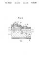
- FIG. 2shows a vertical MIS-SIT as a semiconductor device according to a first embodiment of the present invention, the vertical MIS-SIT using a (111)B face as a substrate crystal face.
- FIGS. 3(a) through 3(d)show a process of manufacturing the semiconductor device according to the first embodiment.
- a substrate crystal 10comprises a n + (111)B face that is highly doped with impurities, i.e., of a high impurity density, and a p layer (or i layer) 11, an n - layer 12, and an n + layer 13 are successively deposited to predetermined thicknesses on the substrate crystal 10 according to the MLE process, thereby producing an S (source) - D (drain) structure.
- n - layer 12 and the p layer (or n layer) 11may be switched around, and the n- and p-type layers in the above structure may be formed of p- and n-type materials, respectively.
- an etching protective filmis formed on the D (drain) or S (source) using a mask pattern, and a gate side 14 which comprises a (111)A face is formed by the photo-excited gas etching or wet etching process.
- the etching process used to etch the (111)A faceis selected such that the etching rate is higher on the (111)B face and lower on the (111)A face.
- the etching processmay be the photo-excited gas etching process using Br 2 or Cl 2 or the wet etching process using a solution of bromethanol, a solution of phosphoric acid, H 2 O 2 , and water, or a solution of sulfuric acid, H 2 O 2 , and water, as shown in Table 2 above.
- an insulating layer 15is deposited on the gate side 14 according to the MO-CVD process.
- the insulating layer 15is formed of a semiconductor material which has a wider band gap than the semiconductor materials of the substrate crystal 10, the p layer (or n layer) 11, the n - layer 12, and the n + layer 13.
- the insulating layer 15serves as an insulator layer in an MIS structure. According to the MO-CVD process, since the growth rate on the (111)B face is 0 as shown in Table 1 above and only the (111)B face and the (111)A face are exposed on the substrate surface, a crystal is grown only on the (111)A face.
- an insulating layer 16is deposited on the substrate crystal 10 according to the MLE process.
- a crystalis grown only on the (111)B face.
- the surface of the n + layer 13being covered with an SiN film or an SiO 2 film, no insulating material is deposited on the SiN film or the SiO 2 film by the MLE process.
- an MIS gate electrode 17is deposited on the insulating layer 16.
- the insulating layer 16is effective to reduce the gate parasitic capacitance between the gate electrode 17 and the substrate crystal 10.
- an insulating layer 18is deposited, and then source, drain, and gate electrodes 19 are deposited, thus completing the vertical MIS-SIT.
- the transistor according to the first embodimentexhibits SIT characteristics because the MLE process employed to form the p layer 11 and the n - layer 12 is capable of controlling the thicknesses of these layers highly accurately in increments of a single molecular layer, and the p layer 11 is of a small thickness.
- the thickness of the p layer 11is several 100 ⁇ or less, electrons injected from the S (source) are not dispersed by the crystal lattice, but reach the D (drain) at a thermal velocity. Consequently, an ultra-high-speed transistor can be produced which has a cutoff frequency of T Hz (tera Hz: 10 12 Hz).
- the thickness of the p layer 11may be reduced down to several ⁇ .
- the insulating layer 15, which serves as an insulator layer in an MIS structure,can be of a highly uniform, ultra-thin-film structure according to the MO-CVD process. Therefore, the semiconductor device can serve as an ultra-high-speed SIT of a low power requirement.
- FIG. 4shows a vertical MIS-SIT as a semiconductor device according to a second embodiment of the present invention, the vertical MIS-SIT using a (111)A face as a substrate crystal face.
- FIGS. 5(a) through 5(d)show a process of manufacturing the semiconductor device according to the second embodiment.
- a substrate crystal 20comprises a highly doped n + (111)A face, and a p layer (or i layer) 21, an n - layer 22, and an n + layer 23 are successively deposited to predetermined thicknesses on the substrate crystal 20 according to the MO-CVD process, thereby producing an S (source) - D (drain) structure.
- n - layer 22 and the p layer (or n layer) 21may be switched around, and the n- and p-type layers in the above structure may be formed of p- and n-type materials, respectively.
- an etching protective filmis formed on the D (drain) or S (source) using a mask pattern, and a gate side 24 which comprises a (111)B face is formed by the photo-excited gas etching or wet etching process.
- the etching process used to etch the (111)B faceis selected such that the etching rate is higher on the (111)A face and lower on the (111)B face.
- the etching processmay be the photo-excited gas etching process using CCl 3 F, PCl 3 , SiCl 4 , or POCl 3 or the wet etching process using a solution of iodine, potassium iodide, and glycerine, as shown in Table 2 above.
- an insulating layer 25is deposited on the gate side 24 according to the MLE process.
- the insulating layer 25is formed of a semiconductor material which has a wider band gap than the semiconductor materials of the substrate crystal 20, the p layer (or n layer) 21, the n - layer 22, and the n + layer 23.
- the insulating layer 25serves as an insulator layer in an MIS structure. According to the MLE process, since the growth rate on the (111)A face is 0 as shown in Table 1 above and only the (111)A face and the (111)B face are exposed on the substrate surface, a crystal is grown only on the (111)B face.
- an insulating layer 26is deposited on the substrate crystal 20 according to the MO-CVD process.
- an MIS gate electrode 27is deposited on the insulating layer 26.
- the insulating layer 26can be deposited only in a given region by the MO-CVD process, as shown in FIG. 4.
- an insulating layer 28is deposited, and then source, drain, and gate electrodes 29 are deposited, thus completing the vertical MIS-SIT.
- the transistor according to the second embodimentexhibits SIT characteristics because the MO-CVD process employed to form the p layer 21 and the n - layer 22 is capable of controlling the thicknesses of these layers in increments of 10 ⁇ , and the p layer 21 is of a small thickness.
- the thickness of the p layer 11may be of several 100 ⁇ or less, electrons injected from the S (source) are not dispersed by the crystal lattice, but reach the D (drain) at a thermal velocity. Consequently, an ultra-high-speed transistor can be produced which has a cutoff frequency of T Hz.
- the insulating layer 25, which serves as an insulator layer in an MIS structure,can be of a highly uniform, ultra-thin-film structure according to the MLE process. Therefore, the semiconductor device can serve as an ultra-high-speed SIT of a low power requirement.
- FIG. 6shows a vertical MIS-SIT as a semiconductor device according to a third embodiment of the present invention, the vertical MIS-SIT using a (110) face as a substrate crystal face.
- FIGS. 7(a) through 7(d)show a process of manufacturing the semiconductor device according to the third embodiment.
- a substrate crystal 30comprises a highly doped n + (110) face, and a p layer (or i layer) 31, an n - layer 32, and an n + layer 33 are successively deposited to predetermined thicknesses on the substrate crystal 30 according to the MO-CVD process, thereby producing an S (source) - D (drain) structure.
- n - layer 32 and the p layer (or n layer) 31may be switched around, and the n- and p-type layers in the above structure may be formed of p- and n-type materials, respectively.
- an etching protective filmis formed on the D (drain) or S (source) using a mask pattern, and a gate side 34 which comprises a (111)B face is formed by the photo-excited gas etching or wet etching process.
- the etching process used to etch the (111)B faceis selected such that the etching rate is higher on the (111)A face and lower on the (111)B face.
- the etching processmay be the photo-excited gas etching process using CCl 3 F, PCl 3 , SiCl 4 , or POCl 3 or the wet etching process using a solution of iodine, potassium iodide, and glycerine, as shown in Table 2 above.
- an insulating layer 35is deposited on the gate side 34 according to the MLE process.
- the insulating layer 35is formed of a semiconductor material which has a wider band gap than the semiconductor materials of the substrate crystal 30, the p layer (or n layer) 31, the n - layer 32, and the n + layer 33.
- the insulating layer 35serves as an insulator layer in an MIS structure. According to the MLE process, since the growth rate on the (111)A face is 0 as shown in Table 1 above and is also 0 on the (110) face, a crystal is grown only on the (111)B face, i.e., the gate side 34.
- an insulating layer 36is deposited on the substrate crystal 30 according to the MO-CVD process.
- an MIS gate electrode 37is deposited on the insulating layer 36.
- the insulating layer 36can be deposited only in a given region by the MO-CVD process, as shown in FIG. 6.
- an insulating layer 38is deposited, and then source, drain, and gate electrodes 39 are deposited, thus completing the vertical MIS-SIT.
- the transistor according to the third embodimentexhibits SIT characteristics because the MO-CVD process employed to form the p layer 21 and the n - layer 22 is capable of controlling the thicknesses of these layers in increments of 10 ⁇ , and the p layer 31 is of a small thickness.
- the thickness of the p layer 11may be of several 100 ⁇ or less.
- electrons injected from the S (source)are not dispersed by the crystal lattice, but reach the D (drain) at a thermal velocity. Consequently, an ultra-high-speed transistor can be produced which has a cutoff frequency of T Hz.
- the insulating layer 35which serves as an insulator layer in an MIS structure, can be of a highly uniform, ultra-thin-film structure according to the MLE process. Therefore, the semiconductor device can serve as an ultra-high-speed SIT of a low power requirement.
- FIG. 8shows a vertical MIS-SIT as a semiconductor device according to a fourth embodiment of the present invention, the vertical MIS-SIT using a (110) face as a substrate crystal face.
- FIGS. 9(a) through 9(e)show a process of manufacturing the semiconductor device according to the fourth embodiment.
- a substrate crystal 40comprises a highly doped n + (110) face, and a side 44' which comprises a (111)A face is formed by the photo-excited gas etching or wet etching process.
- the etching process used to etch the (111)A faceis selected such that the etching rate is higher on the (111)B face and lower on the (111)A face.
- the etching processmay be the photo-excited gas etching process using Br 2 or Cl 2 or the wet etching process using a solution of bromethanol, a solution of phosphoric acid, H 2 O 2 , and water, or a solution of sulfuric acid, H 2 O 2 , and water, as shown in Table 2 above.
- a p layer (or i layer) 41, an n - layer 42, and an n + layer 43are successively deposited to predetermined thicknesses on the side 44' according to the MO-CVD process, thereby producing an S (source) - D (drain) structure.
- n - layer 42 and the p layer (or n layer) 41may be switched around, and the n- and p-type layers in the above structure may be formed of p- and n-type materials, respectively.
- an etching protective filmis formed on the D (drain) or S (source) using a mask pattern, and a gate side 44 which comprises a (111)B face is formed by the photo-excited gas etching or wet etching process.
- the etching process used to etch the (111)B faceis selected such that the etching rate is higher on the (111)A face and lower on the (111)B face.
- the etching processmay be the photo-excited gas etching process using CCl 3 F, PCl 3 , SiCl 4 , or POCl 3 or the wet etching process using a solution of iodine, potassium iodide, and glycerine, as shown in Table 2 above.
- an insulating layer 45is deposited on the gate side 44 according to the MLE process.
- the insulating layer 45is formed of a semiconductor material which has a wider band gap than the semiconductor materials of the substrate crystal 40, the p layer (or n layer) 41, the n - layer 42, and the n + layer 43.
- the insulating layer 15serves as an insulator layer in an MIS structure. According to the MLE process, since the growth rate on the (111)A face and the (110) face is 0 as shown in Table 1 above, a crystal is grown only on the (111)B face, i.e., the gate side 44.
- an insulating layer 46is deposited on the substrate crystal 40 according to the MO-CVD process, and then an MIS gate electrode 47 is deposited on the insulating layer 46.
- the insulating layer 46can be deposited only in a given region by the MO-CVD process, as shown in FIG. 8.
- an insulating layer 48is deposited, and then source, drain, and gate electrodes 49 are deposited, thus completing the vertical MIS-SIT.
- the transistor according to the fourth embodimentexhibits SIT characteristics because the MO-CVD process employed to form the p layer 41 and the n - layer 42 is capable of controlling the thicknesses of these layers in increments of 10 ⁇ , and the p layer 41 is of a small thickness.
- the thickness of the p layer 41may be of several 100 ⁇ or less.
- the insulating layer 45which serves as an insulator layer in an MIS structure, can be of a highly uniform, ultra-thin-film structure according to the MLE process. Therefore, the semiconductor device can serve as an ultra-high-speed SIT of a low power requirement.
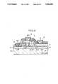
- FIG. 10shows a vertical MIS-SIT as a semiconductor device according to a fifth embodiment of the present invention, the vertical MIS-SIT using a semi-insulating (SI) substrate material as a substrate crystal.
- the vertical MIS-SIT shown in FIG. 9is similar to the vertical MIS-SIT shown in FIG. 2 except that the SI substrate is used to minimize the floating capacitance of the gate.
- the vertical MIS-SIT shown in FIG. 10is manufactured as follows:
- a substrate crystal 50comprises a (111)B face of an SI substrate material.
- n + layer 51, a p layer (or i layer) 11, an n - layer 12, and an n + layer 13are successively deposited to predetermined thicknesses on the substrate crystal 50 according to the MLE process, thereby producing an S (source) - D (drain) structure.
- n - layer 12 and the p layer (or n layer) 11may be switched around, and the n- and p-type layers in the above structure may be formed of p- and n-type materials, respectively.
- an etching protective filmis formed using a mask pattern, and a gate side 14 which comprises a (111)A face is formed by either the photo-excited gas etching using Br 2 or Cl 2 , or the wet etching process using a solution of bromethanol, a solution of phosphoric acid, H 2 O 2 , and water, or a solution of sulfuric acid, H 2 O 2 , and water, as shown in Table 2 above.
- an insulating layer 15is deposited only on the gate side 14 according to the MO-CVD process.
- the insulating layer 15serves as an insulator layer in an MIS structure.
- an insulating layer 16is deposited on the substrate crystal 50 according to the MLE process, and then an MIS gate electrode 17 is deposited on the insulating layer 16.
- an etching protective filmis formed using a mask pattern, and the n + layer 51 is exposed by etching in order to form a source or drain region.
- an insulating layer 18is deposited, and then source, drain, and gate electrodes 19 are deposited, thus completing the vertical MIS-SIT which employs a semi-insulating substrate material as a substrate crystal.
- the thicknesses of these layerscan be controlled highly accurately in increments of a single molecular layer.
- the insulating layer 15, which serves as an insulator layer in an MIS structurecan be of a highly uniform, ultra-thin-film structure according to the MO-CVD process. Since the substrate crystal is of a semi-insulating nature, the capacitance between the gate electrode 17 and the substrate crystal 50 is held to a minimum. Accordingly, the vertical MIS-SIT can operate in a frequency band of T Hz.
- FIG. 10which employs a semi-insulating substrate crystal may be incorporated in the semiconductor devices shown in FIGS. 4, 6, and 8.
- the substrate crystalis formed of GaAs
- the S (source) - D (drain) structureis formed of GaAs
- the insulator layer in the MIS structureis formed of Al x Ga 1-x As.
- the substrate crystalmay be formed of InP
- the S (source) - D (drain) structuremay be formed of Ga x In 1-x As
- the insulator layer in the MIS structuremay be formed of Al x In 1-x As.
- a heterostructure of Ga x In 1-x P/GaAs, Ga x In 1-x As y P 1-y /InP, Ga x In 1-x P/InP, Al x Ga 1-x P/GaP, InAs y Sb 1-y , or the likemay be employed as a material combination in a vertical MIS-SIT.
Landscapes
- Engineering & Computer Science (AREA)
- Physics & Mathematics (AREA)
- Condensed Matter Physics & Semiconductors (AREA)
- General Physics & Mathematics (AREA)
- Manufacturing & Machinery (AREA)
- Computer Hardware Design (AREA)
- Microelectronics & Electronic Packaging (AREA)
- Power Engineering (AREA)
- Junction Field-Effect Transistors (AREA)
- Insulated Gate Type Field-Effect Transistor (AREA)
Abstract
Description
TABLE 1 ______________________________________ Crystal growth process R.sub.(111)B /R.sub.(111)A Remarks ______________________________________ MO-CVD <10.sup.-3 R.sub.(111)A ≈ 400 Å/min. R.sub.(111)B = 0 MLE >10.sup.+3 R.sub.(111)B = 3.26 Å/ cycle(≈ 10 Å/min.) R.sub.(111)A = 0 R.sub.(110) = 0 ______________________________________
TABLE 2 ______________________________________ R'.sub.(111)B / Process Etchant R'.sub.(111)A Remarks ______________________________________ Photo- Br.sub.2 >10.sup.3 R.sub.(111)B ≈ excited 5000 Å/min. gas Cl.sub.2 >10.sup.3 R.sub.(111)B ≈ etching 4000 Å/min. CCl.sub.3 F <10.sup.-3 R.sub.(111)A ≈ 50 Å/min. PCl.sub.3 <10.sup.-3 R.sub.(111)A ≈ 50 Å/min. SiCl.sub.4 <10.sup.-3 R.sub.(111)A ≈ 50 Å/min. POCl.sub.3 <10.sup.-3 R.sub.(111)A ≈ 50 Å/min. Wet Bromethanol >10.sup.3 R.sub.(111)B ≈ etching 2000 Å/min. Phosphoric >10.sup.3 R.sub.(111)B ≈ acid + H.sub.2 O.sub.2 + 200 Å/min. water Iodine + Po- <10.sup.-3 R.sub.(111)A ≈ tassium io- 1000 Å/min. dide + Glycerin Sulfuric acid + >10.sup.2 R.sub.(111)B ≈ H.sub.2 O.sub.2 + water 2000 Å/min. ______________________________________
Claims (4)
Priority Applications (3)
| Application Number | Priority Date | Filing Date | Title |
|---|---|---|---|
| JP2020608AJPH07105497B2 (en) | 1990-01-31 | 1990-01-31 | Semiconductor device and manufacturing method thereof |
| US07/965,722US5296403A (en) | 1990-01-31 | 1992-10-23 | Method of manufacturing a static induction field-effect transistor |
| US08/409,684US5532511A (en) | 1992-10-23 | 1995-03-23 | Semiconductor device comprising a highspeed static induction transistor |
Applications Claiming Priority (2)
| Application Number | Priority Date | Filing Date | Title |
|---|---|---|---|
| JP2020608AJPH07105497B2 (en) | 1990-01-31 | 1990-01-31 | Semiconductor device and manufacturing method thereof |
| US07/965,722US5296403A (en) | 1990-01-31 | 1992-10-23 | Method of manufacturing a static induction field-effect transistor |
Related Child Applications (1)
| Application Number | Title | Priority Date | Filing Date |
|---|---|---|---|
| US16230093ADivision | 1992-10-23 | 1993-12-07 |
Publications (1)
| Publication Number | Publication Date |
|---|---|
| US5296403Atrue US5296403A (en) | 1994-03-22 |
Family
ID=26357579
Family Applications (1)
| Application Number | Title | Priority Date | Filing Date |
|---|---|---|---|
| US07/965,722Expired - LifetimeUS5296403A (en) | 1990-01-31 | 1992-10-23 | Method of manufacturing a static induction field-effect transistor |
Country Status (2)
| Country | Link |
|---|---|
| US (1) | US5296403A (en) |
| JP (1) | JPH07105497B2 (en) |
Cited By (49)
| Publication number | Priority date | Publication date | Assignee | Title |
|---|---|---|---|---|
| US5689127A (en)* | 1996-03-05 | 1997-11-18 | International Business Machines Corporation | Vertical double-gate field effect transistor |
| US6316098B1 (en) | 1998-03-27 | 2001-11-13 | Yissum Research Development Company Of The Hebrew University Of Jerusalem | Molecular layer epitaxy method and compositions |
| US20020083897A1 (en)* | 2000-12-29 | 2002-07-04 | Applied Materials, Inc. | Full glass substrate deposition in plasma enhanced chemical vapor deposition |
| US20030059538A1 (en)* | 2001-09-26 | 2003-03-27 | Applied Materials, Inc. | Integration of barrier layer and seed layer |
| US6551929B1 (en) | 2000-06-28 | 2003-04-22 | Applied Materials, Inc. | Bifurcated deposition process for depositing refractory metal layers employing atomic layer deposition and chemical vapor deposition techniques |
| US20030079686A1 (en)* | 2001-10-26 | 2003-05-01 | Ling Chen | Gas delivery apparatus and method for atomic layer deposition |
| US20030127043A1 (en)* | 2001-07-13 | 2003-07-10 | Applied Materials, Inc. | Pulsed nucleation deposition of tungsten layers |
| US20030132213A1 (en)* | 2000-12-29 | 2003-07-17 | Kim Sam H. | Apparatus and method for uniform substrate heating and contaminate collection |
| US20030153181A1 (en)* | 2002-02-11 | 2003-08-14 | Applied Materials, Inc. | Deposition of tungsten films |
| US20030161952A1 (en)* | 2002-02-26 | 2003-08-28 | Applied Materials, Inc. | Cyclical deposition of tungsten nitride for metal oxide gate electrode |
| US6620670B2 (en) | 2002-01-18 | 2003-09-16 | Applied Materials, Inc. | Process conditions and precursors for atomic layer deposition (ALD) of AL2O3 |
| US6620723B1 (en) | 2000-06-27 | 2003-09-16 | Applied Materials, Inc. | Formation of boride barrier layers using chemisorption techniques |
| US20030190423A1 (en)* | 2002-04-08 | 2003-10-09 | Applied Materials, Inc. | Multiple precursor cyclical deposition system |
| US20030189208A1 (en)* | 2002-04-05 | 2003-10-09 | Kam Law | Deposition of silicon layers for active matrix liquid crystal display (AMLCD) applications |
| US20030189232A1 (en)* | 2002-04-09 | 2003-10-09 | Applied Materials, Inc. | Deposition of passivation layers for active matrix liquid crystal display (AMLCD) applications |
| US20030194825A1 (en)* | 2002-04-10 | 2003-10-16 | Kam Law | Deposition of gate metallization for active matrix liquid crystal display (AMLCD) applications |
| US6660126B2 (en) | 2001-03-02 | 2003-12-09 | Applied Materials, Inc. | Lid assembly for a processing system to facilitate sequential deposition techniques |
| US20040065255A1 (en)* | 2002-10-02 | 2004-04-08 | Applied Materials, Inc. | Cyclical layer deposition system |
| US6720027B2 (en) | 2002-04-08 | 2004-04-13 | Applied Materials, Inc. | Cyclical deposition of a variable content titanium silicon nitride layer |
| US6729824B2 (en) | 2001-12-14 | 2004-05-04 | Applied Materials, Inc. | Dual robot processing system |
| US6734020B2 (en) | 2001-03-07 | 2004-05-11 | Applied Materials, Inc. | Valve control system for atomic layer deposition chamber |
| US6765178B2 (en) | 2000-12-29 | 2004-07-20 | Applied Materials, Inc. | Chamber for uniform substrate heating |
| US20040144999A1 (en)* | 1995-06-07 | 2004-07-29 | Li Chou H. | Integrated circuit device |
| US20040161886A1 (en)* | 1999-08-13 | 2004-08-19 | Leonard Forbes | Vertical sub-micron CMOS transistors on (110), (111), (311), (511), and higher order surfaces of bulk. SOI and thin film structures and method of forming same |
| US6783849B2 (en) | 1998-03-27 | 2004-08-31 | Yissum Research Development Company Of The Hebrew University Of Jerusalem | Molecular layer epitaxy method and compositions |
| US20040209465A1 (en)* | 2000-06-28 | 2004-10-21 | Applied Materials, Inc. | Method and apparatus for depositing refractory metal layers employing sequential deposition techniques to form a nucleation layer |
| US6815278B1 (en)* | 2003-08-25 | 2004-11-09 | International Business Machines Corporation | Ultra-thin silicon-on-insulator and strained-silicon-direct-on-insulator with hybrid crystal orientations |
| US6821563B2 (en) | 2002-10-02 | 2004-11-23 | Applied Materials, Inc. | Gas distribution system for cyclical layer deposition |
| US6875271B2 (en) | 2002-04-09 | 2005-04-05 | Applied Materials, Inc. | Simultaneous cyclical deposition in different processing regions |
| US6878206B2 (en) | 2001-07-16 | 2005-04-12 | Applied Materials, Inc. | Lid assembly for a processing system to facilitate sequential deposition techniques |
| US6911391B2 (en) | 2002-01-26 | 2005-06-28 | Applied Materials, Inc. | Integration of titanium and titanium nitride layers |
| US20050139948A1 (en)* | 2001-09-26 | 2005-06-30 | Applied Materials, Inc. | Integration of barrier layer and seed layer |
| US20050164487A1 (en)* | 2001-02-02 | 2005-07-28 | Applied Materials, Inc. | Formation of a tantalum-nitride layer |
| US20050179096A1 (en)* | 2004-02-12 | 2005-08-18 | Robert Beach | Complimentary nitride transistors vertical and common drain |
| US6998579B2 (en) | 2000-12-29 | 2006-02-14 | Applied Materials, Inc. | Chamber for uniform substrate heating |
| US6998014B2 (en) | 2002-01-26 | 2006-02-14 | Applied Materials, Inc. | Apparatus and method for plasma assisted deposition |
| US7049226B2 (en) | 2001-09-26 | 2006-05-23 | Applied Materials, Inc. | Integration of ALD tantalum nitride for copper metallization |
| US7085616B2 (en) | 2001-07-27 | 2006-08-01 | Applied Materials, Inc. | Atomic layer deposition apparatus |
| US20070009658A1 (en)* | 2001-07-13 | 2007-01-11 | Yoo Jong H | Pulse nucleation enhanced nucleation technique for improved step coverage and better gap fill for WCVD process |
| US20070190780A1 (en)* | 2003-06-18 | 2007-08-16 | Applied Materials, Inc. | Atomic layer deposition of barrier materials |
| US7262133B2 (en) | 2003-01-07 | 2007-08-28 | Applied Materials, Inc. | Enhancement of copper line reliability using thin ALD tan film to cap the copper line |
| US7405158B2 (en) | 2000-06-28 | 2008-07-29 | Applied Materials, Inc. | Methods for depositing tungsten layers employing atomic layer deposition techniques |
| US20080206987A1 (en)* | 2007-01-29 | 2008-08-28 | Gelatos Avgerinos V | Process for tungsten nitride deposition by a temperature controlled lid assembly |
| US20090053893A1 (en)* | 2005-01-19 | 2009-02-26 | Amit Khandelwal | Atomic layer deposition of tungsten materials |
| US7732327B2 (en) | 2000-06-28 | 2010-06-08 | Applied Materials, Inc. | Vapor deposition of tungsten materials |
| US7867914B2 (en) | 2002-04-16 | 2011-01-11 | Applied Materials, Inc. | System and method for forming an integrated barrier layer |
| US20120280308A1 (en)* | 2011-05-02 | 2012-11-08 | Disney Donald R | Vertical power transistor die packages and associated methods of manufacturing |
| CN103474354B (en)* | 2008-12-08 | 2016-12-07 | 住友化学株式会社 | Semiconductor device, the manufacture method of semiconductor device, semiconductor substrate and the manufacture method of semiconductor substrate |
| TWI726004B (en)* | 2015-11-16 | 2021-05-01 | 國立研究開發法人產業技術總合研究所 | Diamond electronic components |
Families Citing this family (5)
| Publication number | Priority date | Publication date | Assignee | Title |
|---|---|---|---|---|
| DE69629760T2 (en)* | 1995-06-16 | 2004-07-08 | Interuniversitair Micro-Electronica Centrum Vzw | Vertical MISFET devices, CMOS process integration, RAM applications |
| JP3528420B2 (en)* | 1996-04-26 | 2004-05-17 | 株式会社デンソー | Semiconductor device and manufacturing method thereof |
| US6977406B2 (en) | 2001-04-27 | 2005-12-20 | National Institute Of Information And Communications Technology, Incorporated Administrative Agency | Short channel insulated-gate static induction transistor and method of manufacturing the same |
| JP3932842B2 (en)* | 2001-08-29 | 2007-06-20 | 株式会社デンソー | Silicon carbide semiconductor device and manufacturing method thereof |
| JP4085603B2 (en)* | 2001-08-29 | 2008-05-14 | 株式会社デンソー | Silicon carbide semiconductor device and manufacturing method thereof |
Citations (9)
| Publication number | Priority date | Publication date | Assignee | Title |
|---|---|---|---|---|
| US3865625A (en)* | 1972-10-13 | 1975-02-11 | Bell Telephone Labor Inc | Molecular beam epitaxy shadowing technique for fabricating dielectric optical waveguides |
| GB2068168A (en)* | 1980-01-26 | 1981-08-05 | Ferranti Ltd | Bipolar transistor |
| US4473598A (en)* | 1982-06-30 | 1984-09-25 | International Business Machines Corporation | Method of filling trenches with silicon and structures |
| US4642144A (en)* | 1983-10-06 | 1987-02-10 | Exxon Research And Engineering Company | Proximity doping of amorphous semiconductors |
| US4713358A (en)* | 1986-05-02 | 1987-12-15 | Gte Laboratories Incorporated | Method of fabricating recessed gate static induction transistors |
| US4883770A (en)* | 1986-09-19 | 1989-11-28 | Hewlett-Packard Company | Selective NIPI doping super lattice contacts and other semiconductor device structures formed by shadow masking fabrication |
| US5106770A (en)* | 1990-11-16 | 1992-04-21 | Gte Laboratories Incorporated | Method of manufacturing semiconductor devices |
| US5180684A (en)* | 1989-03-08 | 1993-01-19 | Fujitsu Limited | Semiconductor growth process |
| US5236863A (en)* | 1992-06-01 | 1993-08-17 | National Semiconductor Corporation | Isolation process for VLSI |
Family Cites Families (5)
| Publication number | Priority date | Publication date | Assignee | Title |
|---|---|---|---|---|
| JPS56104474A (en)* | 1980-01-23 | 1981-08-20 | Semiconductor Res Found | Silicon semiconductor device |
| JPH06101566B2 (en)* | 1984-04-25 | 1994-12-12 | 株式会社日立製作所 | Vertical field effect transistor |
| JPS5918678A (en)* | 1982-07-21 | 1984-01-31 | Sony Corp | Manufacturing method for semiconductor devices |
| JPS59222964A (en)* | 1983-06-01 | 1984-12-14 | Matsushita Electric Ind Co Ltd | Semiconductor device |
| JPS60101974A (en)* | 1983-11-08 | 1985-06-06 | Toshiba Corp | Semiconductor device |
- 1990
- 1990-01-31JPJP2020608Apatent/JPH07105497B2/ennot_activeExpired - Fee Related
- 1992
- 1992-10-23USUS07/965,722patent/US5296403A/ennot_activeExpired - Lifetime
Patent Citations (9)
| Publication number | Priority date | Publication date | Assignee | Title |
|---|---|---|---|---|
| US3865625A (en)* | 1972-10-13 | 1975-02-11 | Bell Telephone Labor Inc | Molecular beam epitaxy shadowing technique for fabricating dielectric optical waveguides |
| GB2068168A (en)* | 1980-01-26 | 1981-08-05 | Ferranti Ltd | Bipolar transistor |
| US4473598A (en)* | 1982-06-30 | 1984-09-25 | International Business Machines Corporation | Method of filling trenches with silicon and structures |
| US4642144A (en)* | 1983-10-06 | 1987-02-10 | Exxon Research And Engineering Company | Proximity doping of amorphous semiconductors |
| US4713358A (en)* | 1986-05-02 | 1987-12-15 | Gte Laboratories Incorporated | Method of fabricating recessed gate static induction transistors |
| US4883770A (en)* | 1986-09-19 | 1989-11-28 | Hewlett-Packard Company | Selective NIPI doping super lattice contacts and other semiconductor device structures formed by shadow masking fabrication |
| US5180684A (en)* | 1989-03-08 | 1993-01-19 | Fujitsu Limited | Semiconductor growth process |
| US5106770A (en)* | 1990-11-16 | 1992-04-21 | Gte Laboratories Incorporated | Method of manufacturing semiconductor devices |
| US5236863A (en)* | 1992-06-01 | 1993-08-17 | National Semiconductor Corporation | Isolation process for VLSI |
Cited By (118)
| Publication number | Priority date | Publication date | Assignee | Title |
|---|---|---|---|---|
| US20040144999A1 (en)* | 1995-06-07 | 2004-07-29 | Li Chou H. | Integrated circuit device |
| US5780327A (en)* | 1996-03-05 | 1998-07-14 | International Business Machines Corporation | Vertical double-gate field effect transistor |
| US5689127A (en)* | 1996-03-05 | 1997-11-18 | International Business Machines Corporation | Vertical double-gate field effect transistor |
| US6316098B1 (en) | 1998-03-27 | 2001-11-13 | Yissum Research Development Company Of The Hebrew University Of Jerusalem | Molecular layer epitaxy method and compositions |
| US6808803B1 (en) | 1998-03-27 | 2004-10-26 | Yissum Research Development Company Of The Hebrew University Of Jerusalem | Molecular epitaxy method and compositions |
| US20040202875A1 (en)* | 1998-03-27 | 2004-10-14 | Yissum Res & Dev Co Of Hebrew Univ Of Jerusalem | Molecular epitaxy method and compositions |
| US6783849B2 (en) | 1998-03-27 | 2004-08-31 | Yissum Research Development Company Of The Hebrew University Of Jerusalem | Molecular layer epitaxy method and compositions |
| US7217606B2 (en)* | 1999-08-13 | 2007-05-15 | Micron Technology, Inc. | Method of forming vertical sub-micron CMOS transistors on (110), (111), (311), (511), and higher order surfaces of bulk, soi and thin film structures |
| US20040161886A1 (en)* | 1999-08-13 | 2004-08-19 | Leonard Forbes | Vertical sub-micron CMOS transistors on (110), (111), (311), (511), and higher order surfaces of bulk. SOI and thin film structures and method of forming same |
| US7208413B2 (en) | 2000-06-27 | 2007-04-24 | Applied Materials, Inc. | Formation of boride barrier layers using chemisorption techniques |
| US20050118804A1 (en)* | 2000-06-27 | 2005-06-02 | Applied Materials, Inc. | Formation of boride barrier layers using chemisorption techniques |
| US7501344B2 (en) | 2000-06-27 | 2009-03-10 | Applied Materials, Inc. | Formation of boride barrier layers using chemisorption techniques |
| US6620723B1 (en) | 2000-06-27 | 2003-09-16 | Applied Materials, Inc. | Formation of boride barrier layers using chemisorption techniques |
| US7501343B2 (en) | 2000-06-27 | 2009-03-10 | Applied Materials, Inc. | Formation of boride barrier layers using chemisorption techniques |
| US7465666B2 (en) | 2000-06-28 | 2008-12-16 | Applied Materials, Inc. | Method for forming tungsten materials during vapor deposition processes |
| US7235486B2 (en) | 2000-06-28 | 2007-06-26 | Applied Materials, Inc. | Method for forming tungsten materials during vapor deposition processes |
| US20090156004A1 (en)* | 2000-06-28 | 2009-06-18 | Moris Kori | Method for forming tungsten materials during vapor deposition processes |
| US20080280438A1 (en)* | 2000-06-28 | 2008-11-13 | Ken Kaung Lai | Methods for depositing tungsten layers employing atomic layer deposition techniques |
| US7745333B2 (en) | 2000-06-28 | 2010-06-29 | Applied Materials, Inc. | Methods for depositing tungsten layers employing atomic layer deposition techniques |
| US7732327B2 (en) | 2000-06-28 | 2010-06-08 | Applied Materials, Inc. | Vapor deposition of tungsten materials |
| US20100093170A1 (en)* | 2000-06-28 | 2010-04-15 | Applied Materials, Inc. | Method for forming tungsten materials during vapor deposition processes |
| US6855368B1 (en) | 2000-06-28 | 2005-02-15 | Applied Materials, Inc. | Method and system for controlling the presence of fluorine in refractory metal layers |
| US7405158B2 (en) | 2000-06-28 | 2008-07-29 | Applied Materials, Inc. | Methods for depositing tungsten layers employing atomic layer deposition techniques |
| US7846840B2 (en) | 2000-06-28 | 2010-12-07 | Applied Materials, Inc. | Method for forming tungsten materials during vapor deposition processes |
| US7033922B2 (en) | 2000-06-28 | 2006-04-25 | Applied Materials. Inc. | Method and system for controlling the presence of fluorine in refractory metal layers |
| US20060128132A1 (en)* | 2000-06-28 | 2006-06-15 | Applied Materials, Inc. | Method and system for controlling the presence of fluorine in refractory metal layers |
| US6551929B1 (en) | 2000-06-28 | 2003-04-22 | Applied Materials, Inc. | Bifurcated deposition process for depositing refractory metal layers employing atomic layer deposition and chemical vapor deposition techniques |
| US20040209465A1 (en)* | 2000-06-28 | 2004-10-21 | Applied Materials, Inc. | Method and apparatus for depositing refractory metal layers employing sequential deposition techniques to form a nucleation layer |
| US7115494B2 (en) | 2000-06-28 | 2006-10-03 | Applied Materials, Inc. | Method and system for controlling the presence of fluorine in refractory metal layers |
| US7101795B1 (en) | 2000-06-28 | 2006-09-05 | Applied Materials, Inc. | Method and apparatus for depositing refractory metal layers employing sequential deposition techniques to form a nucleation layer |
| US7674715B2 (en) | 2000-06-28 | 2010-03-09 | Applied Materials, Inc. | Method for forming tungsten materials during vapor deposition processes |
| US20050150459A1 (en)* | 2000-12-29 | 2005-07-14 | Quanyuan Shang | Full glass substrate deposition in plasma enhanced chemical vapor deposition |
| US6825447B2 (en) | 2000-12-29 | 2004-11-30 | Applied Materials, Inc. | Apparatus and method for uniform substrate heating and contaminate collection |
| US20020083897A1 (en)* | 2000-12-29 | 2002-07-04 | Applied Materials, Inc. | Full glass substrate deposition in plasma enhanced chemical vapor deposition |
| US20040255861A1 (en)* | 2000-12-29 | 2004-12-23 | Quanyuan Shang | Chamber for uniform substrate heating |
| US6765178B2 (en) | 2000-12-29 | 2004-07-20 | Applied Materials, Inc. | Chamber for uniform substrate heating |
| US7022948B2 (en) | 2000-12-29 | 2006-04-04 | Applied Materials, Inc. | Chamber for uniform substrate heating |
| US20030132213A1 (en)* | 2000-12-29 | 2003-07-17 | Kim Sam H. | Apparatus and method for uniform substrate heating and contaminate collection |
| US6998579B2 (en) | 2000-12-29 | 2006-02-14 | Applied Materials, Inc. | Chamber for uniform substrate heating |
| US20050164487A1 (en)* | 2001-02-02 | 2005-07-28 | Applied Materials, Inc. | Formation of a tantalum-nitride layer |
| US6951804B2 (en) | 2001-02-02 | 2005-10-04 | Applied Materials, Inc. | Formation of a tantalum-nitride layer |
| US20060030148A1 (en)* | 2001-02-02 | 2006-02-09 | Applied Materials, Inc. | Formation of a tantalum-nitride layer |
| US20100311237A1 (en)* | 2001-02-02 | 2010-12-09 | Seutter Sean M | Formation of a tantalum-nitride layer |
| US7781326B2 (en) | 2001-02-02 | 2010-08-24 | Applied Materials, Inc. | Formation of a tantalum-nitride layer |
| US9012334B2 (en) | 2001-02-02 | 2015-04-21 | Applied Materials, Inc. | Formation of a tantalum-nitride layer |
| US7094680B2 (en) | 2001-02-02 | 2006-08-22 | Applied Materials, Inc. | Formation of a tantalum-nitride layer |
| US8114789B2 (en) | 2001-02-02 | 2012-02-14 | Applied Materials, Inc. | Formation of a tantalum-nitride layer |
| US6660126B2 (en) | 2001-03-02 | 2003-12-09 | Applied Materials, Inc. | Lid assembly for a processing system to facilitate sequential deposition techniques |
| US9587310B2 (en) | 2001-03-02 | 2017-03-07 | Applied Materials, Inc. | Lid assembly for a processing system to facilitate sequential deposition techniques |
| US7201803B2 (en) | 2001-03-07 | 2007-04-10 | Applied Materials, Inc. | Valve control system for atomic layer deposition chamber |
| US6734020B2 (en) | 2001-03-07 | 2004-05-11 | Applied Materials, Inc. | Valve control system for atomic layer deposition chamber |
| US20030127043A1 (en)* | 2001-07-13 | 2003-07-10 | Applied Materials, Inc. | Pulsed nucleation deposition of tungsten layers |
| US20080317954A1 (en)* | 2001-07-13 | 2008-12-25 | Xinliang Lu | Pulsed deposition process for tungsten nucleation |
| US7211144B2 (en) | 2001-07-13 | 2007-05-01 | Applied Materials, Inc. | Pulsed nucleation deposition of tungsten layers |
| US20070009658A1 (en)* | 2001-07-13 | 2007-01-11 | Yoo Jong H | Pulse nucleation enhanced nucleation technique for improved step coverage and better gap fill for WCVD process |
| US7695563B2 (en) | 2001-07-13 | 2010-04-13 | Applied Materials, Inc. | Pulsed deposition process for tungsten nucleation |
| US20050115675A1 (en)* | 2001-07-16 | 2005-06-02 | Gwo-Chuan Tzu | Lid assembly for a processing system to facilitate sequential deposition techniques |
| US7905959B2 (en) | 2001-07-16 | 2011-03-15 | Applied Materials, Inc. | Lid assembly for a processing system to facilitate sequential deposition techniques |
| US6878206B2 (en) | 2001-07-16 | 2005-04-12 | Applied Materials, Inc. | Lid assembly for a processing system to facilitate sequential deposition techniques |
| US20110114020A1 (en)* | 2001-07-16 | 2011-05-19 | Gwo-Chuan Tzu | Lid assembly for a processing system to facilitate sequential deposition techniques |
| US10280509B2 (en) | 2001-07-16 | 2019-05-07 | Applied Materials, Inc. | Lid assembly for a processing system to facilitate sequential deposition techniques |
| US7085616B2 (en) | 2001-07-27 | 2006-08-01 | Applied Materials, Inc. | Atomic layer deposition apparatus |
| US7494908B2 (en) | 2001-09-26 | 2009-02-24 | Applied Materials, Inc. | Apparatus for integration of barrier layer and seed layer |
| US6936906B2 (en) | 2001-09-26 | 2005-08-30 | Applied Materials, Inc. | Integration of barrier layer and seed layer |
| US20030059538A1 (en)* | 2001-09-26 | 2003-03-27 | Applied Materials, Inc. | Integration of barrier layer and seed layer |
| US20060148253A1 (en)* | 2001-09-26 | 2006-07-06 | Applied Materials, Inc. | Integration of ALD tantalum nitride for copper metallization |
| US20050139948A1 (en)* | 2001-09-26 | 2005-06-30 | Applied Materials, Inc. | Integration of barrier layer and seed layer |
| US7049226B2 (en) | 2001-09-26 | 2006-05-23 | Applied Materials, Inc. | Integration of ALD tantalum nitride for copper metallization |
| US7352048B2 (en) | 2001-09-26 | 2008-04-01 | Applied Materials, Inc. | Integration of barrier layer and seed layer |
| US8668776B2 (en) | 2001-10-26 | 2014-03-11 | Applied Materials, Inc. | Gas delivery apparatus and method for atomic layer deposition |
| US20030079686A1 (en)* | 2001-10-26 | 2003-05-01 | Ling Chen | Gas delivery apparatus and method for atomic layer deposition |
| US7780788B2 (en) | 2001-10-26 | 2010-08-24 | Applied Materials, Inc. | Gas delivery apparatus for atomic layer deposition |
| US6916398B2 (en) | 2001-10-26 | 2005-07-12 | Applied Materials, Inc. | Gas delivery apparatus and method for atomic layer deposition |
| US6729824B2 (en) | 2001-12-14 | 2004-05-04 | Applied Materials, Inc. | Dual robot processing system |
| US6620670B2 (en) | 2002-01-18 | 2003-09-16 | Applied Materials, Inc. | Process conditions and precursors for atomic layer deposition (ALD) of AL2O3 |
| US7473638B2 (en) | 2002-01-26 | 2009-01-06 | Applied Materials, Inc. | Plasma-enhanced cyclic layer deposition process for barrier layers |
| US7779784B2 (en) | 2002-01-26 | 2010-08-24 | Applied Materials, Inc. | Apparatus and method for plasma assisted deposition |
| US6998014B2 (en) | 2002-01-26 | 2006-02-14 | Applied Materials, Inc. | Apparatus and method for plasma assisted deposition |
| US7732325B2 (en) | 2002-01-26 | 2010-06-08 | Applied Materials, Inc. | Plasma-enhanced cyclic layer deposition process for barrier layers |
| US20060075966A1 (en)* | 2002-01-26 | 2006-04-13 | Applied Materials, Inc. | Apparatus and method for plasma assisted deposition |
| US20060292864A1 (en)* | 2002-01-26 | 2006-12-28 | Yang Michael X | Plasma-enhanced cyclic layer deposition process for barrier layers |
| US6911391B2 (en) | 2002-01-26 | 2005-06-28 | Applied Materials, Inc. | Integration of titanium and titanium nitride layers |
| US7094685B2 (en) | 2002-01-26 | 2006-08-22 | Applied Materials, Inc. | Integration of titanium and titanium nitride layers |
| US20030153181A1 (en)* | 2002-02-11 | 2003-08-14 | Applied Materials, Inc. | Deposition of tungsten films |
| US6827978B2 (en) | 2002-02-11 | 2004-12-07 | Applied Materials, Inc. | Deposition of tungsten films |
| US6833161B2 (en) | 2002-02-26 | 2004-12-21 | Applied Materials, Inc. | Cyclical deposition of tungsten nitride for metal oxide gate electrode |
| US7115499B2 (en) | 2002-02-26 | 2006-10-03 | Applied Materials, Inc. | Cyclical deposition of tungsten nitride for metal oxide gate electrode |
| US20070020924A1 (en)* | 2002-02-26 | 2007-01-25 | Shulin Wang | Tungsten nitride atomic layer deposition processes |
| US20080305629A1 (en)* | 2002-02-26 | 2008-12-11 | Shulin Wang | Tungsten nitride atomic layer deposition processes |
| US20050176240A1 (en)* | 2002-02-26 | 2005-08-11 | Shulin Wang | Cyclical deposition of tungsten nitride for metal oxide gate electrode |
| US20030161952A1 (en)* | 2002-02-26 | 2003-08-28 | Applied Materials, Inc. | Cyclical deposition of tungsten nitride for metal oxide gate electrode |
| US7429516B2 (en) | 2002-02-26 | 2008-09-30 | Applied Materials, Inc. | Tungsten nitride atomic layer deposition processes |
| US7745329B2 (en) | 2002-02-26 | 2010-06-29 | Applied Materials, Inc. | Tungsten nitride atomic layer deposition processes |
| US20030189208A1 (en)* | 2002-04-05 | 2003-10-09 | Kam Law | Deposition of silicon layers for active matrix liquid crystal display (AMLCD) applications |
| US7439191B2 (en) | 2002-04-05 | 2008-10-21 | Applied Materials, Inc. | Deposition of silicon layers for active matrix liquid crystal display (AMLCD) applications |
| US6846516B2 (en) | 2002-04-08 | 2005-01-25 | Applied Materials, Inc. | Multiple precursor cyclical deposition system |
| US20030190423A1 (en)* | 2002-04-08 | 2003-10-09 | Applied Materials, Inc. | Multiple precursor cyclical deposition system |
| US6720027B2 (en) | 2002-04-08 | 2004-04-13 | Applied Materials, Inc. | Cyclical deposition of a variable content titanium silicon nitride layer |
| US20030189232A1 (en)* | 2002-04-09 | 2003-10-09 | Applied Materials, Inc. | Deposition of passivation layers for active matrix liquid crystal display (AMLCD) applications |
| US6869838B2 (en) | 2002-04-09 | 2005-03-22 | Applied Materials, Inc. | Deposition of passivation layers for active matrix liquid crystal display (AMLCD) applications |
| US6875271B2 (en) | 2002-04-09 | 2005-04-05 | Applied Materials, Inc. | Simultaneous cyclical deposition in different processing regions |
| US20030194825A1 (en)* | 2002-04-10 | 2003-10-16 | Kam Law | Deposition of gate metallization for active matrix liquid crystal display (AMLCD) applications |
| US7867914B2 (en) | 2002-04-16 | 2011-01-11 | Applied Materials, Inc. | System and method for forming an integrated barrier layer |
| US6821563B2 (en) | 2002-10-02 | 2004-11-23 | Applied Materials, Inc. | Gas distribution system for cyclical layer deposition |
| US20040065255A1 (en)* | 2002-10-02 | 2004-04-08 | Applied Materials, Inc. | Cyclical layer deposition system |
| US7262133B2 (en) | 2003-01-07 | 2007-08-28 | Applied Materials, Inc. | Enhancement of copper line reliability using thin ALD tan film to cap the copper line |
| US7595263B2 (en) | 2003-06-18 | 2009-09-29 | Applied Materials, Inc. | Atomic layer deposition of barrier materials |
| US20070190780A1 (en)* | 2003-06-18 | 2007-08-16 | Applied Materials, Inc. | Atomic layer deposition of barrier materials |
| US6815278B1 (en)* | 2003-08-25 | 2004-11-09 | International Business Machines Corporation | Ultra-thin silicon-on-insulator and strained-silicon-direct-on-insulator with hybrid crystal orientations |
| US8193612B2 (en) | 2004-02-12 | 2012-06-05 | International Rectifier Corporation | Complimentary nitride transistors vertical and common drain |
| US20050179096A1 (en)* | 2004-02-12 | 2005-08-18 | Robert Beach | Complimentary nitride transistors vertical and common drain |
| US7964505B2 (en) | 2005-01-19 | 2011-06-21 | Applied Materials, Inc. | Atomic layer deposition of tungsten materials |
| US20090053893A1 (en)* | 2005-01-19 | 2009-02-26 | Amit Khandelwal | Atomic layer deposition of tungsten materials |
| US20080206987A1 (en)* | 2007-01-29 | 2008-08-28 | Gelatos Avgerinos V | Process for tungsten nitride deposition by a temperature controlled lid assembly |
| CN103474354B (en)* | 2008-12-08 | 2016-12-07 | 住友化学株式会社 | Semiconductor device, the manufacture method of semiconductor device, semiconductor substrate and the manufacture method of semiconductor substrate |
| US20120280308A1 (en)* | 2011-05-02 | 2012-11-08 | Disney Donald R | Vertical power transistor die packages and associated methods of manufacturing |
| US8742490B2 (en)* | 2011-05-02 | 2014-06-03 | Monolithic Power Systems, Inc. | Vertical power transistor die packages and associated methods of manufacturing |
| TWI726004B (en)* | 2015-11-16 | 2021-05-01 | 國立研究開發法人產業技術總合研究所 | Diamond electronic components |
Also Published As
| Publication number | Publication date |
|---|---|
| JPH07105497B2 (en) | 1995-11-13 |
| JPH0482275A (en) | 1992-03-16 |
Similar Documents
| Publication | Publication Date | Title |
|---|---|---|
| US5296403A (en) | Method of manufacturing a static induction field-effect transistor | |
| US5532511A (en) | Semiconductor device comprising a highspeed static induction transistor | |
| US5504353A (en) | Field effect transistor | |
| US5179037A (en) | Integration of lateral and vertical quantum well transistors in the same epitaxial stack | |
| KR19980024988A (en) | Integrated CMOS circuit apparatus and its manufacturing method | |
| WO2002031886A1 (en) | Monolithically integrated e/d mode hemt and method for fabricating the same | |
| JPS634955B2 (en) | ||
| JPH0624208B2 (en) | Semiconductor device | |
| KR930011474B1 (en) | Semiconductor device and manufacturing method thereof | |
| US5686735A (en) | Silicon-on-insulator (SOI) transistor | |
| JPH11103046A (en) | Field effect transistor and method of manufacturing the same | |
| JPS5915388B2 (en) | semiconductor equipment | |
| JP2758803B2 (en) | Field effect transistor | |
| JPS62271475A (en) | Semiconductor device | |
| US4442445A (en) | Planar doped barrier gate field effect transistor | |
| JP2709374B2 (en) | Insulated gate field effect semiconductor device | |
| US5107314A (en) | Gallium antimonide field-effect transistor | |
| US4689646A (en) | Depletion mode two-dimensional electron gas field effect transistor and the method for manufacturing the same | |
| US3450960A (en) | Insulated-gate field effect transistor with nonplanar gate electrode structure for optimizing transconductance | |
| JP2701583B2 (en) | Tunnel transistor and manufacturing method thereof | |
| JP2626220B2 (en) | Field effect transistor and method of manufacturing the same | |
| JPS6394682A (en) | Manufacture of insulated-gate field-effect semiconductor device | |
| JP3653652B2 (en) | Semiconductor device | |
| JP3304343B2 (en) | Field effect transistor | |
| JPH01270275A (en) | Semiconductor device |
Legal Events
| Date | Code | Title | Description |
|---|---|---|---|
| AS | Assignment | Owner name:NISHIZAWA, JUN-ICHI, JAPAN Free format text:ASSIGNMENT OF ASSIGNORS INTEREST.;ASSIGNORS:NISHIZAWA, JUN-ICHI;KURABAYASHI, TORU;REEL/FRAME:006301/0361 Effective date:19921007 Owner name:RESEARCH DEVELOPMENT A CORP. OF JAPAN, JAPAN Free format text:ASSIGNMENT OF ASSIGNORS INTEREST.;ASSIGNORS:NISHIZAWA, JUN-ICHI;KURABAYASHI, TORU;REEL/FRAME:006301/0361 Effective date:19921007 Owner name:ZAIDAN HOJIN HANDOTAI KENKYU SHINKOKAI, JAPAN Free format text:ASSIGNMENT OF ASSIGNORS INTEREST.;ASSIGNORS:NISHIZAWA, JUN-ICHI;KURABAYASHI, TORU;REEL/FRAME:006301/0361 Effective date:19921007 | |
| STCF | Information on status: patent grant | Free format text:PATENTED CASE | |
| FPAY | Fee payment | Year of fee payment:4 | |
| FEPP | Fee payment procedure | Free format text:PAYOR NUMBER ASSIGNED (ORIGINAL EVENT CODE: ASPN); ENTITY STATUS OF PATENT OWNER: LARGE ENTITY | |
| FPAY | Fee payment | Year of fee payment:8 | |
| FPAY | Fee payment | Year of fee payment:12 | |
| AS | Assignment | Owner name:JAPAN SCIENCE AND DEVELOPMENT AGENCY, JAPAN Free format text:ASSIGNMENT OF ASSIGNORS INTEREST;ASSIGNORS:NISHIZAWA, JUN-ICHI;ZAIDAN HOJIN HANDOTAI KENKYU SHINKOKAI;REEL/FRAME:021212/0137 Effective date:20080331 Owner name:TOHOKU UNIVERSITY, JAPAN Free format text:ASSIGNMENT OF ASSIGNORS INTEREST;ASSIGNORS:NISHIZAWA, JUN-ICHI;ZAIDAN HOJIN HANDOTAI KENKYU SHINKOKAI;REEL/FRAME:021212/0137 Effective date:20080331 |