US5295174A - Shifting circuit and shift register - Google Patents
Shifting circuit and shift registerDownload PDFInfo
- Publication number
- US5295174A US5295174AUS07/795,501US79550191AUS5295174AUS 5295174 AUS5295174 AUS 5295174AUS 79550191 AUS79550191 AUS 79550191AUS 5295174 AUS5295174 AUS 5295174A
- Authority
- US
- United States
- Prior art keywords
- circuit
- circuits
- holding
- signals
- latch
- Prior art date
- Legal status (The legal status is an assumption and is not a legal conclusion. Google has not performed a legal analysis and makes no representation as to the accuracy of the status listed.)
- Expired - Lifetime
Links
Images


Classifications
- G—PHYSICS
- G11—INFORMATION STORAGE
- G11C—STATIC STORES
- G11C19/00—Digital stores in which the information is moved stepwise, e.g. shift registers
Definitions
- the present inventionrelates to a shifting circuit for shifting time digital signals series in sequence, to output the shifted signals, and a shift resistor employing the same.
- a shift registeris widely used to delay a serial signal and output the signal, or as one means for performing the serial to parallel conversion.
- a shifting circuit used with the prior art shift registeris constructed by flip-flop circuits employing NAND circuits or NOR circuits, or by flip-flop circuits having two latch circuits connected in series.
- JP-A-2-105396 (1990) by Akiyama et al.discloses a shift register in which a plurality of memory cells each being constructed by two latch circuits are connected in series.
- the shifting circuit constructed by such a flip-flop circuitrequires for example about sixteen transistor devices per stage in the case where a master-slave flip-flop is used. Since the shift register is constructed by connecting such shifting circuits in series by the number of shifting stages, for example, in the case where the shift register having a thousand stages is manufactured, there is required one thousand flip-flop circuits or two thousand latch circuits. Therefore, the number of devices making up the shift resister becomes very enormous, so that the prior art shift register is not suitable for higher integration. This is one problem.
- the present inventionwas made in order to solve the above problems and it is therefore an object of the present invention to provide a newly developed shifting circuit which is suitable for the higher integration and with lower power consumption, and a shift register employing the same.
- a shifting circuit used for a shift registerfor delaying time series signals inputted thereto by a predetermined timing and output the delayed time series signal, comprising:
- a clock control circuitfor generating latch clocks and selection clocks
- latch circuitshaving respective output terminals and respective input terminals connected in parallel with the input line, the latch circuits serving to latch the input signals synchronistically with the respective latch clocks to output the input signals;
- a multiplexerhaving input terminals connected to the respective output terminals of the latch circuits, the multiplexer serving to select outputs of the latch circuits in sequence synchronistically with the respective selection clocks to provide the outputs on the output line in sequence,
- the clock control circuitdelays the selection clock used for selecting the output from a certain latch circuit with respect to the latch clock synchronistically with which the certain latch circuit latchs the input signal by the predetermined timing.
- the present inventionalso provides a shift register constructed by connecting the above shifting circuits in series.
- the provided number of the latch circuitslatch the input signals such as time series digital signals in sequence.
- a predetermined timing after the latch timing when the individual circuits latched the respective signalsthe multiplexer read out in sequence the signals latched in the latch circuits to provide the signals thus read out on the output terminal in sequence.
- the delay of the reading out timingcan be selected up to the clock number which is the same number as that of the latch circuits.
- the shifting circuit of the present inventionis constructed by one latch circuit with respect to the shifting operation of one stage, it can be constructed by the elements the number of which is approximately one-half, as compared with the case where the prior art circuit requires two latch circuits for example, with respect to the shifting operation of one stage.
- the shift register of the present inventionsince in the shift register of the present invention, the number of elements is reduced, it is possible to attain higher integration. Moreover, since during the operation of the shift register, only some elements which are selected with the clock signals from the clock control circuit are simultaneously operated, electric energy which is consumed at the same time is excessively reduced. Thus, the shift register of the present invention is suitable for higher integration.
- FIG. 1is a block diagram showing the arrangement of one shifting circuit of the present invention
- FIG. 2is a block diagram showing the relationship in arrangement between latch circuits and a multiplexer in another shifting circuit of the present invention
- FIG. 3is a block diagram showing the arrangement of a clock control circuit in the example shown in FIG. 2;
- FIG. 4is a timing chart explaining the operation of the shifting circuit shown in FIG. 2 and FIG. 3;
- FIG. 5is a block diagram showing the arrangement of a shift register of the present invention.
- FIG. 1is a block diagram showing the arrangement of one embodiment of a shifting circuit of the present invention.
- the reference numeral 1designates an input terminal to which time series signals Xj are supplied.
- the reference numerals 2-1, . . . , 2-i, . . . , and 2-ndesignate n latch circuits LA, respectively, of which input terminals are connected in common to the input terminals 1.
- the reference numeral 3designates a multiplexer MP of which input terminals are connected to output terminals of the individual latch circuits, respectively.
- the reference numeral 4designates a clock control circuit CL which supplies each of the latch circuits 2-1, . . . , 2-i, . . . , and 2-n with latch clocks CK and the multiplexer 3 with selection clocks M.
- the reference numeral 5designates an output terminal for providing therethrough outputs from the multiplexer 3.
- the latch circuits 2-1, . . . , and 2-nlatch n time series signals Xn+1, . . . , and X2n, respectively.
- the group of time series signalsis latched by the latch circuits 2-1, . . . , 2-n.
- the multiplexer 3serves to enable the input gates which are connected to the output terminals of the latch circuits LA (2-1, . . . , 2-i, . . . , . . . and 2-n), respectively, in turn synchronistically with the selection clocks M which are supplied to the multiplexer 3 by the clock control circuit 4. Moreover, the multiplexer 3 serves to fetch the signals latched in the latch circuits to output them in the form of time series signals Yj to the output terminal.
- the timing of the selection clock M used for driving the input gate of the multiplexer connected to the output terminal of a certain latch circuitis delayed with respect to the timing of the latch clock CK used for driving the input gates of the certain latch circuit, by a predetermined pulse number k of which maximum value is n. Therefore, the shifting circuit of the present invention delays the time series signals Xj supplied to the input terminals by a predetermined timing, that is, k bits, to provide that signal in the form of time series output signals Yj through the output terminal 5.
- the shifting circuit of the present inventionserving to delay the input signals by a predetermined timing of which maximum value is n bits is made up of n latch circuits, one multiplexer, and one clock control circuit.
- a 1 bit-shift register of the prior artrequires two latch circuits, in addition to a peripheral circuit, and an n bit-shift register thereof requires 2n latch circuits, whereas the shifting circuit of present invention is made up of the extremely lower number of elements.
- FIG. 2is a block diagram showing the arrangement of a latch circuit and a multiplexer in an example of a 2-bit-shifting circuit of the present invention.
- FIG. 3is a block diagram showing the arrangement of a clock control circuit.
- FIG. 4is a timing chart for explaining the operation of the example shown in FIG. 2 and FIG. 3.
- the reference numerals 11 and 12designate latch circuits for receiving input signal D IN at respective input terminals
- the reference numeral 31designates an AND circuit for receiving an output Q0 from the latch circuit 11
- the reference numeral 32designates an AND circuit for receiving an output Q1 from the latch circuit 12
- the reference numeral 33designates an OR circuit for receiving outputs from the AND circuits 31 and 32 to provide the received output as an output D OUT of the shifting circuit.
- the multiplexeris made up of the AND circuits and the OR circuit.
- Each of the latch circuits 11 and 12may be constructed by six field effect transistors.
- the reference numeral 41designates a D flip-flop
- the reference numerals 42 and 43designate AND circuits.
- the clock control circuitis made up of the D flip-flop and the AND circuits.
- a terminal D of the flip-flop circuitis connected to an inversion output terminal Q.
- An output terminal Q of the flip-flop circuitis connected to one input terminal of the AND circuit 42, and the inversion output terminal Q thereof is connected to one input terminal of the AND circuit 42.
- a terminal CK of the flip-flop circuit 41is connected to each of the other input terminals of the AND circuits 42 and 43.
- a reference clock CLKis supplied from the externals of the circuit to the terminal CK of the D flip-flop circuit 41.
- the clock CLKis divided with frequency by the flip-flop circuit 41 so that a clock M having a frequency of one-half of that of CLK is provided at the output terminal Q.
- This clock Mbecomes a selection clock M1 and is supplied together with the AND circuit 42 of the clock control circuit to the AND circuit 32 of the multiplexer.
- a clock into which the clock M is inverted with the phase thereofis provided at the inversion output terminal Q.
- This clockbecomes a selection clock M0 which is delayed with respect to the selection clock M1 by one pulse and is supplied together with the AND circuit 43 of the clock control circuit to the AND circuit 32 of the multiplexer.
- the clock pulse M1function as a gate pulse for the AND circuit 42.
- the pulse portion in which the clock pulse M1 and the reference clock CLK have the positive potential in commonis provided as a latch clock CK0 to the output terminal of the circuit 42.
- the pulse portion in which the clock pulse M0 provided at the inversion output terminal Q and the reference clock CLK have the positive potential in commonis provided as a latch clock CK1 to the output terminal of the AND circuit 43.
- the latch clock pulses CK0 and CK1are out of phase and in the 2 bit-shifting circuit of the present invention, the selection clock pulses M0 and M1 are respectively delayed with respect to the latch clock pulses CK0 and CK1 by one pulse.
- the latch clock CK0is inputted to the latch circuit 11 and the signals D0, D2, D4, . . . out of the input signals D IN (D0, D1, D2, D3, . . . ), which are present at the time of rise of the clock CK0, are latched in sequence in the circuit 11. Therefore, the time series signals consisting of the signals D0, D2, D4, . . . are provided at the output terminal Q0 of the latch circuit 11.
- the latch clock CK1is inputted to the latch circuit 12 and the signals D1, D3, D5, . . . out of the input signals D IN (D0, D1, D2, D3, . . . ), which are present at the time of rise of the clock CK1, are provided in sequence at the output terminal Q1 of the latch circuit 12.
- the selection clock M0activates the AND circuit 31 so that the signal Q0 is outputted as the output D OUT through the OR circuit 33.
- the selection clock M1activates the AND circuit 32 so that the output signal Q1 is outputted as the output D OUT through the OR circuit 33.
- the OR circuit 33composes the output signal Q0, that is, the group of the signals D0, D2, D4, . . . and the output signal Q1, that is, the group of the signals D1, D3, D5, . . . to output the composite signal as one-pulse delayed output signal D OUT , that is, the group of signals D0, D1, D2, D3, D4, . . . .
- the input signal D1is latched in the latch circuit 11 and is provided as the output Q0. Since the selection signal M0 is at the high potential, that signal D1 is provided as the output signal D OUT through the AND circuit 31 and the OR circuit 33. Then, when the latch clock CK1 rises, the latch circuit 12 is triggered, the input signal D2 is fetched in the circuit 12 to be latched therein and the signal D2 is provided as the output Q1 from the latch circuit 12. However, since the selection clock M1 is at the low potential, the output of the AND circuit is maintained at the low potential. Next, when the selection clock M0 is changed to the low potential, the output of the AND circuit 31 becomes the low potential irrespective of the input.
- the multiplexeroutputs the output D2 of the latch circuit 12 through the AND circuit 32 and the OR circuit 33.
- the input signal D INis changed to the signal D3, and when the latch clock CK0 subsequently rises, the signal D3 is fetched in the latch circuit 11 to be latched therein.
- the input signal D INbecomes the output signal D OUT being delayed by one pulse.
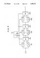
- FIG. 5is a schematic block diagram showing a shift register of the present invention which is constructed using the shifting circuit of the present invention shown in FIG. 1.
- the figureillustrates the arrangement in which the shifting circuits of eight stages are connected in series.
- the reference numerals 102 and 103designate the first stage of a latch circuit group and a multiplexer, respectively
- the reference numerals 202 and 203designate the second stage of a latch circuit group and a multiplexer, respectively
- the reference numerals 802 and 803designate the eighth stage of a latch circuit group and a multiplexer, respectively
- the reference numeral 40designates a clock control circuit.
- the latch circuit group in each of the stagesis made up of n latch circuits and has the same arrangement in each stage.
- One clock control circuit 40is provided for the whole shift register, which supplies a common latch clock CK to the latch circuit group in each of the stages, and supplies in common the multiplexer in each stage with a selection clock M which is delayed with respect to the latch clock CK by k bits.
- the shift register of the present inventionwhich is arranged in such a manner, it is possible to perform the shift the maximum quantity of which is 8 ⁇ n bits. Further, by adjusting the delay timing of the selection clock M from the clock control circuit 40, an 8 ⁇ k bit-shift register is obtained. For example, a circuit employing eight 16 bit-shifting circuits makes up a 128 bit-shift register.
- the shift register of the present inventionmay also be constructed for shifting by 1,000 bits adapted for an image processor by increasing the number of latch circuits in each stage and by increasing the number of stages.
- the shift register of the present inventionwhich is constructed by integrating such shifting circuits can be manufactured as a preferable integrated circuit which is small in size and has the less power consumption.
Landscapes
- Shift Register Type Memory (AREA)
Abstract
Description
Claims (7)
Applications Claiming Priority (2)
| Application Number | Priority Date | Filing Date | Title |
|---|---|---|---|
| JP31951890 | 1990-11-21 | ||
| JP2-319518 | 1990-11-21 |
Publications (1)
| Publication Number | Publication Date |
|---|---|
| US5295174Atrue US5295174A (en) | 1994-03-15 |
Family
ID=18111124
Family Applications (1)
| Application Number | Title | Priority Date | Filing Date |
|---|---|---|---|
| US07/795,501Expired - LifetimeUS5295174A (en) | 1990-11-21 | 1991-11-21 | Shifting circuit and shift register |
Country Status (2)
| Country | Link |
|---|---|
| US (1) | US5295174A (en) |
| JP (1) | JPH0520887A (en) |
Cited By (22)
| Publication number | Priority date | Publication date | Assignee | Title |
|---|---|---|---|---|
| US5424654A (en)* | 1994-09-22 | 1995-06-13 | Kaplinsky; Cecil H. | Programmable macrocell circuit |
| US5426380A (en)* | 1994-09-30 | 1995-06-20 | Sun Microsystems, Inc. | High speed processing flip-flop |
| US5477172A (en)* | 1994-12-12 | 1995-12-19 | Advanced Micro Devices, Inc. | Configurable input buffer dependent on supply voltage |
| US5497117A (en)* | 1994-03-03 | 1996-03-05 | Kabushiki Kaisha Toshiba | Input sense circuit having selectable thresholds |
| US5534799A (en)* | 1992-08-31 | 1996-07-09 | Nec Corporation | Compact flag control circuit capable of producing a zero flag in a short time |
| US5552745A (en)* | 1994-09-21 | 1996-09-03 | International Business Machines Corporation | Self-resetting CMOS multiplexer with static output driver |
| US5706323A (en)* | 1996-03-01 | 1998-01-06 | Hewlett-Packard Company | Dynamic 1-of-2N logic encoding |
| US5761266A (en)* | 1996-11-22 | 1998-06-02 | National Semiconductor Corporation | Shifter circuit that emulates a barrel shifter |
| US5781056A (en)* | 1995-09-27 | 1998-07-14 | Ando Electric Co., Ltd. | Variable delay circuit |
| US5790894A (en)* | 1994-06-14 | 1998-08-04 | Texas Instruments Incorporated | Data processing with improved register bit structure |
| US5796288A (en)* | 1995-05-16 | 1998-08-18 | Hewlett-Packard Company | Graphics accelerator having minimal logic multiplexer system for sharing a microprocessor |
| EP0889481A1 (en)* | 1997-07-04 | 1999-01-07 | STMicroelectronics SA | Improvements of sequential access memories |
| FR2765718A1 (en)* | 1997-07-04 | 1999-01-08 | Sgs Thomson Microelectronics | Low energy consumption memory for holding information in smart card |
| WO1999060574A1 (en)* | 1998-05-18 | 1999-11-25 | Telefonaktiebolaget Lm Ericsson | Low power linear feedback shift registers |
| US6054884A (en)* | 1998-01-23 | 2000-04-25 | Pmc - Sierra Ltd. | Process-insensitive controllable CMOS delay line |
| US6496050B2 (en)* | 2000-06-21 | 2002-12-17 | Stmicroelectronics Limited | Selective modification of clock pulses |
| US20050031068A1 (en)* | 2003-08-04 | 2005-02-10 | Johnny Chan | Shift register with reduced area and power consumption |
| US7042895B1 (en)* | 1999-09-24 | 2006-05-09 | Agere Systems Inc. | Method and apparatus for interfacing multiple communication devices to a time division multiplexing bus |
| KR100594317B1 (en) | 2005-01-28 | 2006-06-30 | 삼성전자주식회사 | Shift register with low power consumption and operation method of the shift register |
| CN100428359C (en)* | 2002-11-20 | 2008-10-22 | 海力士半导体有限公司 | Pipeline latch circuit for high-speed output data |
| US8604949B2 (en) | 2011-10-27 | 2013-12-10 | Sharp Kabushiki Kaisha | Serial-to-parallel converter, and display device incorporating the same |
| CN111667873A (en)* | 2019-03-05 | 2020-09-15 | 爱思开海力士有限公司 | Shift Register |
Families Citing this family (3)
| Publication number | Priority date | Publication date | Assignee | Title |
|---|---|---|---|---|
| KR100711968B1 (en)* | 2006-11-01 | 2007-05-02 | (주)에이프러스 씨엠 건축사사무소 | Drainage and Landscaping Structure Installation Structure for Apartment House |
| US7567471B2 (en)* | 2006-12-21 | 2009-07-28 | Intel Corporation | High speed fanned out system architecture and input/output circuits for non-volatile memory |
| US8994424B2 (en) | 2013-03-12 | 2015-03-31 | International Business Machines Corporation | Distributing multiplexing logic to remove multiplexor latency on the output path for variable clock cycle, delayed signals |
Citations (8)
| Publication number | Priority date | Publication date | Assignee | Title |
|---|---|---|---|---|
| US3421092A (en)* | 1965-10-22 | 1969-01-07 | Hughes Aircraft Co | Multirank multistage shift register |
| US3753241A (en)* | 1970-11-26 | 1973-08-14 | Sperry Rand Ltd | Shift register having internal buffer |
| US4627085A (en)* | 1984-06-29 | 1986-12-02 | Applied Micro Circuits Corporation | Flip-flop control circuit |
| US4837790A (en)* | 1986-10-24 | 1989-06-06 | Clarion, Co., Ltd. | Maximum length linearly occurring code sequence generator |
| US4852130A (en)* | 1986-09-02 | 1989-07-25 | Siemens Aktiengesellschaft | Successive approximation register |
| US4876704A (en)* | 1986-12-22 | 1989-10-24 | Nec Corporation | Logic integrated circuit for scan path system |
| JPH02105396A (en)* | 1988-10-13 | 1990-04-17 | Nec Corp | Shift register |
| US5150389A (en)* | 1990-01-26 | 1992-09-22 | Kabushiki Kaisha Toshiba | Shift register |
- 1991
- 1991-11-21USUS07/795,501patent/US5295174A/ennot_activeExpired - Lifetime
- 1991-11-21JPJP3332606Apatent/JPH0520887A/enactivePending
Patent Citations (8)
| Publication number | Priority date | Publication date | Assignee | Title |
|---|---|---|---|---|
| US3421092A (en)* | 1965-10-22 | 1969-01-07 | Hughes Aircraft Co | Multirank multistage shift register |
| US3753241A (en)* | 1970-11-26 | 1973-08-14 | Sperry Rand Ltd | Shift register having internal buffer |
| US4627085A (en)* | 1984-06-29 | 1986-12-02 | Applied Micro Circuits Corporation | Flip-flop control circuit |
| US4852130A (en)* | 1986-09-02 | 1989-07-25 | Siemens Aktiengesellschaft | Successive approximation register |
| US4837790A (en)* | 1986-10-24 | 1989-06-06 | Clarion, Co., Ltd. | Maximum length linearly occurring code sequence generator |
| US4876704A (en)* | 1986-12-22 | 1989-10-24 | Nec Corporation | Logic integrated circuit for scan path system |
| JPH02105396A (en)* | 1988-10-13 | 1990-04-17 | Nec Corp | Shift register |
| US5150389A (en)* | 1990-01-26 | 1992-09-22 | Kabushiki Kaisha Toshiba | Shift register |
Cited By (29)
| Publication number | Priority date | Publication date | Assignee | Title |
|---|---|---|---|---|
| US5534799A (en)* | 1992-08-31 | 1996-07-09 | Nec Corporation | Compact flag control circuit capable of producing a zero flag in a short time |
| US5497117A (en)* | 1994-03-03 | 1996-03-05 | Kabushiki Kaisha Toshiba | Input sense circuit having selectable thresholds |
| US5790894A (en)* | 1994-06-14 | 1998-08-04 | Texas Instruments Incorporated | Data processing with improved register bit structure |
| US5552745A (en)* | 1994-09-21 | 1996-09-03 | International Business Machines Corporation | Self-resetting CMOS multiplexer with static output driver |
| US5568076A (en)* | 1994-09-21 | 1996-10-22 | International Business Machines Corporation | Method of converting short duration input pulses to longer duration output pulses |
| US5424654A (en)* | 1994-09-22 | 1995-06-13 | Kaplinsky; Cecil H. | Programmable macrocell circuit |
| US5426380A (en)* | 1994-09-30 | 1995-06-20 | Sun Microsystems, Inc. | High speed processing flip-flop |
| US5477172A (en)* | 1994-12-12 | 1995-12-19 | Advanced Micro Devices, Inc. | Configurable input buffer dependent on supply voltage |
| US5796288A (en)* | 1995-05-16 | 1998-08-18 | Hewlett-Packard Company | Graphics accelerator having minimal logic multiplexer system for sharing a microprocessor |
| US5781056A (en)* | 1995-09-27 | 1998-07-14 | Ando Electric Co., Ltd. | Variable delay circuit |
| US5706323A (en)* | 1996-03-01 | 1998-01-06 | Hewlett-Packard Company | Dynamic 1-of-2N logic encoding |
| US5761266A (en)* | 1996-11-22 | 1998-06-02 | National Semiconductor Corporation | Shifter circuit that emulates a barrel shifter |
| FR2765718A1 (en)* | 1997-07-04 | 1999-01-08 | Sgs Thomson Microelectronics | Low energy consumption memory for holding information in smart card |
| EP0889481A1 (en)* | 1997-07-04 | 1999-01-07 | STMicroelectronics SA | Improvements of sequential access memories |
| US5963505A (en)* | 1997-07-04 | 1999-10-05 | Sgs-Thomson Microelectronics, S.A. | Sequential access memory with low consumption |
| US5978295A (en)* | 1997-07-04 | 1999-11-02 | Stmicroelectronics S.A. | Sequential access memories |
| FR2765719A1 (en)* | 1997-07-04 | 1999-01-08 | Sgs Thomson Microelectronics | IMPROVEMENT IN MEMORIES WITH SEQUENTIAL ACCESS |
| US6054884A (en)* | 1998-01-23 | 2000-04-25 | Pmc - Sierra Ltd. | Process-insensitive controllable CMOS delay line |
| WO1999060574A1 (en)* | 1998-05-18 | 1999-11-25 | Telefonaktiebolaget Lm Ericsson | Low power linear feedback shift registers |
| US6442579B1 (en) | 1998-05-18 | 2002-08-27 | Telefonaktiebolaget Lm Ericsson | Low power linear feedback shift registers |
| US7042895B1 (en)* | 1999-09-24 | 2006-05-09 | Agere Systems Inc. | Method and apparatus for interfacing multiple communication devices to a time division multiplexing bus |
| US6496050B2 (en)* | 2000-06-21 | 2002-12-17 | Stmicroelectronics Limited | Selective modification of clock pulses |
| CN100428359C (en)* | 2002-11-20 | 2008-10-22 | 海力士半导体有限公司 | Pipeline latch circuit for high-speed output data |
| US6891917B2 (en) | 2003-08-04 | 2005-05-10 | Atmel Corporation | Shift register with reduced area and power consumption |
| US20050031068A1 (en)* | 2003-08-04 | 2005-02-10 | Johnny Chan | Shift register with reduced area and power consumption |
| KR100594317B1 (en) | 2005-01-28 | 2006-06-30 | 삼성전자주식회사 | Shift register with low power consumption and operation method of the shift register |
| US8604949B2 (en) | 2011-10-27 | 2013-12-10 | Sharp Kabushiki Kaisha | Serial-to-parallel converter, and display device incorporating the same |
| CN111667873A (en)* | 2019-03-05 | 2020-09-15 | 爱思开海力士有限公司 | Shift Register |
| CN111667873B (en)* | 2019-03-05 | 2023-04-04 | 爱思开海力士有限公司 | Shift register |
Also Published As
| Publication number | Publication date |
|---|---|
| JPH0520887A (en) | 1993-01-29 |
Similar Documents
| Publication | Publication Date | Title |
|---|---|---|
| US5295174A (en) | Shifting circuit and shift register | |
| CN100362593C (en) | Shift Register | |
| JP3361925B2 (en) | Integrated circuit | |
| JP2862592B2 (en) | Display device | |
| CN110912549A (en) | A serial-parallel conversion circuit and its driving method, and a display panel | |
| JP2006259753A (en) | Static clock pulse generator and display | |
| US20020005793A1 (en) | Serial/parallel converter | |
| JP2576366B2 (en) | Variable delay buffer circuit | |
| CN111224658A (en) | A design method of conversion circuit from parallel data to serial data | |
| GB2221072A (en) | Programmable sequential-code recognition circuit | |
| US5508967A (en) | Line memory | |
| US6064232A (en) | Self-clocked logic circuit and methodology | |
| US5227790A (en) | Cascaded drive units having low power consumption | |
| EP0506418B1 (en) | Display driver circuit | |
| US5359636A (en) | Register control circuit for initialization of registers | |
| US5627795A (en) | Timing generating device | |
| US8264264B2 (en) | Multiple phase pulse generator | |
| US4387294A (en) | Shift register-latch circuit driven by clocks with half cycle phase deviation and usable with a serial alu | |
| US4672647A (en) | Serial data transfer circuits for delayed output | |
| US5392229A (en) | Graphics processing apparatus with video memory for storing graphics data | |
| CN112799465B (en) | Control signal generator and driving method thereof | |
| US4337526A (en) | Monolithically integrable semiconductor memory | |
| JP2869339B2 (en) | Line memory | |
| JP2923175B2 (en) | Clock generation circuit | |
| JPH08297475A (en) | Liquid crystal display device and its driving method |
Legal Events
| Date | Code | Title | Description |
|---|---|---|---|
| AS | Assignment | Owner name:NIPPON STEEL CORPORATION A CORP. OF JAPAN, JAPAN Free format text:ASSIGNMENT OF ASSIGNORS INTEREST.;ASSIGNOR:SHIMIZU, SHIN;REEL/FRAME:005922/0296 Effective date:19911111 | |
| FPAY | Fee payment | Year of fee payment:4 | |
| REMI | Maintenance fee reminder mailed | ||
| REIN | Reinstatement after maintenance fee payment confirmed | ||
| FP | Lapsed due to failure to pay maintenance fee | Effective date:20020315 | |
| AS | Assignment | Owner name:UNITED MICROELECTRONICS CORPORATION, TAIWAN Free format text:ASSIGNMENT OF ASSIGNORS INTEREST;ASSIGNOR:NIPPON STEEL CORPORATION;REEL/FRAME:013011/0300 Effective date:20010129 | |
| FEPP | Fee payment procedure | Free format text:PAYOR NUMBER ASSIGNED (ORIGINAL EVENT CODE: ASPN); ENTITY STATUS OF PATENT OWNER: LARGE ENTITY Free format text:PAYER NUMBER DE-ASSIGNED (ORIGINAL EVENT CODE: RMPN); ENTITY STATUS OF PATENT OWNER: LARGE ENTITY | |
| FEPP | Fee payment procedure | Free format text:PETITION RELATED TO MAINTENANCE FEES FILED (ORIGINAL EVENT CODE: PMFP); ENTITY STATUS OF PATENT OWNER: LARGE ENTITY Free format text:PETITION RELATED TO MAINTENANCE FEES GRANTED (ORIGINAL EVENT CODE: PMFG); ENTITY STATUS OF PATENT OWNER: LARGE ENTITY | |
| FEPP | Fee payment procedure | Free format text:PAYOR NUMBER ASSIGNED (ORIGINAL EVENT CODE: ASPN); ENTITY STATUS OF PATENT OWNER: LARGE ENTITY | |
| PRDP | Patent reinstated due to the acceptance of a late maintenance fee | Effective date:20030314 | |
| FPAY | Fee payment | Year of fee payment:8 | |
| SULP | Surcharge for late payment | ||
| STCF | Information on status: patent grant | Free format text:PATENTED CASE | |
| FPAY | Fee payment | Year of fee payment:12 |