US5293628A - Data processing system which generates a waveform with improved pulse width resolution - Google Patents
Data processing system which generates a waveform with improved pulse width resolutionDownload PDFInfo
- Publication number
- US5293628A US5293628AUS07/787,167US78716791AUS5293628AUS 5293628 AUS5293628 AUS 5293628AUS 78716791 AUS78716791 AUS 78716791AUS 5293628 AUS5293628 AUS 5293628A
- Authority
- US
- United States
- Prior art keywords
- signal
- value
- counter
- logic state
- duty control
- Prior art date
- Legal status (The legal status is an assumption and is not a legal conclusion. Google has not performed a legal analysis and makes no representation as to the accuracy of the status listed.)
- Expired - Lifetime
Links
Images

Classifications
- G—PHYSICS
- G06—COMPUTING OR CALCULATING; COUNTING
- G06F—ELECTRIC DIGITAL DATA PROCESSING
- G06F1/00—Details not covered by groups G06F3/00 - G06F13/00 and G06F21/00
- G06F1/02—Digital function generators
- G06F1/025—Digital function generators for functions having two-valued amplitude, e.g. Walsh functions
Definitions
- the present inventionrelates in general to data processors, and more particularly to waveform generation in a digital data processor.
- Microcomputers todayare used to control a wide variety of products ranging from a simple household appliance to a complex automobile.
- One of the important uses carried out by the microcomputeris timing control. Timing control can also range from the very simple to the very complex.
- a household appliancemay only require a microcomputer timer to count how much time has elapsed between two events in order to control the appliance.
- An automobileon the other hand, may require the timer to generate or recognize complex waveforms in order to control the automobile engine.
- timerAn important use for timer functions, other than control, is the generation of clocks for communication systems. Communication systems transfer data between multiple locations. Some communication systems require one or more clocks in order to determine when the various bits of data are to be sent.
- a timeris a convenient device which can be used to generate the clocks required by a communication system. A timer can also be used to generate a wide range of output waveforms that can be used for purposes other than control and the clocking of communication information.
- Period and cycleare being used synonymously in this document.
- the period or cycle of a waveformis the length of time between any two rising edges or any two falling edges of the waveform.
- the pulse width of a waveformis the length of time that the pulse remains in a predetermined state, either high or low.
- the duty cycle of a waveformis the percentage of time that the waveform is high during the total waveform period. For example, a waveform that has a 70% duty cycle is high for 70% of the total period and low for the remaining 30% of the period. A waveform that has a 50% duty cycle is high for 50% of the total period and low for the remaining 50% of the period. And a waveform with a 20% duty cycle is high for 20% of the total period and low for the remaining 80% of the period.
- timersoperate by using an input clock, a counter, and some type of compare logic.
- the counteris used to keep track of the length of time that has elapsed from an initial starting time.
- the counteris incremented by the first edge of the input clock.
- the contents of the counterare compared to a preprogrammed value to determine if the two values match. If a match occurs, the timer has determined that a sufficient length of time has elapsed since the initial starting time. The timer then performs the appropriate function, such as causing an interrupt or driving a value on an output pin. If a match does not occur, the timer has determined that a sufficient time has not elapsed since the initial starting time and the counter is again incremented on the next edge of the input clock.
- the compare operationmust be performed after each increment of the counter. If a compare is not performed after each increment, a match may occur and yet go undetected.
- the countercan only be incremented once during each period of the input clock.
- a standard counter with an input clock frequency of "F”can only count at the rate of "F”. For example, a counter with an input clock of 6 megahertz can only count at the rate of 6 megahertz.
- the rate at which a counter can countdetermines the resolution of the timer.
- the resolution of existing timersis limited by the frequency of the input clock.
- Many microcomputer customerswant timers that have greater resolution.
- the easy solution of merely increasing the frequency of the input clock in order to increase the resolution of the timeris usually not a viable option.
- the input clock to the timeris usually the fastest system clock operating throughout the entire microcomputer. Increasing the speed of this system clock affects all parts of the system, not just the timer. Some circuitry within the microcomputer will not operate correctly above a certain maximum frequency, and this maximum frequency may not be great enough to produce the required resolution in the timer.
- the present inventioncomprises an apparatus and a method for generating an output signal with a reduced pulse width resolution period.
- the data processing systemcomprises a data processor for providing a control signal, a clock generator for providing a clock signal of predetermined period, and a logic means.
- the logic meanshas a clock input coupled to the clock signal, a control input coupled to the data processor for receiving the control signal, and an output signal.
- the output signalhas a pulse width determined by the control signal, and a pulse width resolution period which is equal to the predetermined period of the clock divided by a power of two.
- the logic meansselectively adjusts the output signal by a predetermined amount in order to lengthen the output signal in response to the control signal.
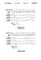
- FIG. 1Aillustrates, in timing diagram form, output waveforms generated by a prior art device
- FIG. 1Billustrates, in timing diagram form, output waveforms generated by one embodiment of the present invention
- FIG. 2illustrates, in block diagram form, a data processing system having circuitry with a reduced pulse width resolution period in accordance with one embodiment of the present invention
- FIG. 3illustrates, in block diagram form, a high resolution counter module of FIG. 2 in accordance with one embodiment of the present invention
- FIG. 4illustrates, in partial logic diagram form, a resolution selection logic circuit of FIG. 3 in accordance with one embodiment of the present invention.
- FIG. 5illustrates, in partial logic diagram form, a waveform completion and edge adjust logic circuit of FIG. 3 in accordance with one embodiment of the present invention.
- assertand “negate” will be used when referring to the rendering of a signal, status bit, or similar apparatus into its logically true or logically false state, respectively.
- the symbol “%” preceding a numberindicates that the number is represented in its binary or base two form.
- FIG. 1Aillustrates output waveforms A, B, and C which are generated by a prior art timing device.
- the prior art timing devicehas a pulse width resolution period (PWRP) equal to one period of the input clock.
- PWRPpulse width resolution period
- Pulse width resolution periodis a characteristic of a device that generates waveforms, it is not a characteristic of a single waveform itself.
- the PWRP of a deviceis determined by comparing the duration of two pulses that have as close to the same pulse widths as the device is capable of producing. For example, referring to the prior art in FIG. 1A, the durations of the pulse widths of waveforms A, B, and C are as close to the same pulse width as the prior art timing device is capable of producing.
- the pulse widths of the shortest pulse (output waveform A) and the next shortest pulse (output waveform B)are compared. The difference in duration of the two pulses is the length of time labeled "PWRP".
- the PWRP of the prior art timing deviceis equal to one period of the input clock.
- the timing device's PWRPremsins constant for all other waveforms that the device generates using the same configuration. For example, output waveforms B and C also differ in duration by one period of the input clock.
- the pulse width resolution period of a deviceis measured in units of time and for many applications it is advantageous for a device to have as small a PWRP as possible.
- a smaller PWRPallows a device to generate pulses with intermediate pulse widths that cannot be generated by a device with a larger PWRP.
- These intermediate pulse widthsmay be required by certain peripheral devices, such as stepper motors or communication receivers, which are receiving and using the pulses generated by the timing device.
- FIG. 1Aillustrates output waveforms A, B, and C which are generated by a prior art timing device.
- the prior art deviceuses the input clock signal as an input to a three-bit counter (not shown).
- the counteris incremented on every other edge of the input clock signal.
- Each arrow in FIG. 1Aindicates an increment of the counter.
- the numbers above the arrowsindicate the value that is contained in the counter before the increment takes place.
- the three-bit counterstarts with the value of 0 and increments by one until the counter contains the maximum count value of 7. When the counter contains the value 7 and is incremented by one, the counter rolls over to 0.
- the remaining edges of the input clockin this example the rising edges, are used for a compare operation (not shown) and cannot be used to increment the counter.
- FIG. 1Billustrates the improvement over the prior art which is provided by the present invention.
- An approachwas needed that increased the resolution of the timer without requiring an increase in the frequency of the input clock to the timer.
- FIG. 1Billustrates output waveforms D, E, and F which are generated by one embodiment of the present invention.
- This embodimentuses the same input clock signal as the prior art.
- the input clock signalis used as an input to a four-bit counter (not shown).
- the counteris incremented on every other edge of the input clock signal.
- Each arrow in FIG. 1Bindicates an increment of the counter.
- the numbers above the arrowsindicate the value that is contained in the counter before the increment takes place.
- the four-bit counterstarts with the value of 0 and counts up to the value 14 by increments of two. When the counter contains the value 14 and is incremented by two, the counter rolls over to 0.
- the remaining edges of the input clockin this example the rising edges, are used for a compare operation (not shown) and cannot be used to increment the counter.
- the PWRP illustrated in FIG. 1Bis equal to one-half of one period of the input clock and was generated by one embodiment of the present invention.
- the PWRP of the illustrated embodimentis one-half of the PWRP of the prior art using the same input clock period. This is a significant improvement over the prior art.
- the present inventionallows a prior art device to be modified by a small amount of circuitry in order to produce a doubling of performance. Decreasing the PWRP of a device from a full period of the input clock to one-half a period of the input clock is a doubling of performance.
- the performance improvement illustrated in FIG. 1Bis only double that of the prior art, the present invention will also permit a four times increase in performance, an eight times increase in performance, and in fact a 2 N increase in performance where N is an integer.
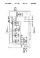
- FIG. 2illustrates a data processing system 10 which has a data processor 12, a clock generator 14, and a high resolution counter module 16.
- High resolution counter module 16may optionally be part of the timer or serial subsystem 18 within data processing system 10.
- Clock generator 14generates an input clock 20 which is an input to high resolution counter module 16.
- High resolution counter module 16generates an output waveform 22.
- Data processor 12outputs several control signals to high resolution counter module 16, including duty control signals 24, a resolution control signal 26, a polarity signal 28, and a reset signal 30.
- duty control signals 24are multiple signals, but other embodiments may use only one signal to transmit duty control information from the data processor 12 to the high resolution counter module 16.
- the present inventionrequires that duty control information be transmitted from the data processor 12 to the high resolution counter module 16.
- the remaining control signals, resolution control signal 26, polarity signal 28, and reset signal 30,are optional. These three optional control signals are used in the present embodiment of the invention, but they are not required.
- the high resolution counter module 16uses the input clock 20 and all of the control inputs from data processor 12 in order to generate the output waveform 22.
- Output waveform 22can be generated so that it has a pulse width resolution period (PWRP) that is equal to the period of the input clock 20 divided by a power of two.
- PWRPpulse width resolution period
- Similar prior art devicescan only generate output waveforms with a PWRP that is equal to the period of the input clock 20.
- a smaller PWRPallows a device to generate pulses with intermediate pulse widths that cannot be generated by a device with a larger PWRP. These intermediate pulse widths may be required by certain peripheral devices, such as stepper motors or communication receivers, which are receiving and using the pulses generated by the timing device.
- FIG. 3illustrates in greater detail the structure of the high resolution counter module 16 of FIG. 2.
- High resolution counter module 16contains a duty compare logic 32, a counter 34, a resolution selection logic 36, and a waveform completion and edge adjustment logic 38.
- Counter 34contains N counter stage circuits, of which four counter stage circuits, counter stage 0 circuit 40a, counter stage 1 circuit 40b, counter stage 2 circuit 40c, and counter stage N circuit 40d, are illustrated.
- Duty compare logic 32receives duty control signals 24 as inputs. Also, duty compare logic 32 receives, as inputs, the contents of each counter stage, counter stage 0 circuit 40a, counter stage 1 circuit 40b, counter stage 2 circuit 40c, and counter stage N circuit 40d. Duty compare logic 32 generates two output signals, a duty compare match 42 and an edge adjust 44, which are inputs to the waveform completion and edge adjustment logic 38.
- Resolution control signal 26is an input to both the resolution selection logic 36 and the waveform completion and edge adjustment logic 38.
- Input clock 20is likewise an input to both the resolution selection logic 36 and the waveform completion and edge adjustment logic 38.
- Resolution selection logic 36outputs STAGE 0 IN signal 46 as an input to counter stage 0 circuit 40a.
- resolution selection logic 36outputs STAGE 1 IN signal 48 as an input to counter stage 1 circuit 40b.
- Counter stage 0 circuit 40aoutputs STAGE 0 OUT signal 50 as an input to resolution selection logic 36.
- Counter stage N circuit 40doutputs an end of period signal 52 as an input to the waveform completion and edge adjustment logic 38.
- Polarity signal 28 and reset signal 30are both inputs to the waveform completion and edge adjustment logic 38.
- Waveform completion and edge adjustment logic 38generates output waveform 22.
- FIG. 3illustrates an N-stage or N-bit counter
- the particular embodiment that will be describedwill be a four-bit counter that is able to produce the output waveforms illustrated in FIG. 1B.
- counter 34performs a counting function.
- One of the counter stagesreceives the input clock 20 as an input. Which counter stage receives the input clock 20 as an input determines whether the counter 34 counts or increments by one, by two, by four, or by 2 N .
- input clock 20has two edges. On the first edge of input clock 20, the counter is incremented by either one, two, four, or 2 N . On the second edge of input clock 20, the contents of counter 34 (i.e. the contents of each counter stage 40a, 40b, 40c, and 40d) are compared to a user programmed value in duty compare logic 32 in order to determine if there is a match. On the next first edge of input clock 20, the counter is again incremented and this cycle of increment and compare is continued until a match is found.
- the contents of counter 34i.e. the contents of each counter stage 40a, 40b, 40c, and 40d
- the duty compare match signal 42is asserted to indicate that the logic state of output waveform 22 should be inverted by the waveform completion and edge adjustment logic 38.
- the counter 34continues to count. When counter 34 reaches its maximum count value and rolls over to its lowest count value, counter stage N circuit 40d produces an end of period signal 52 which indicates that the end of the period of the output waveform 22 has been reached and that the logic state of output waveform 22 should once again be inverted by the waveform completion and edge adjustment logic 38. Consequently, the period of the output waveform 22 is determined by the amount of time it takes for counter 34 to increment from its lowest count value to its maximum count value and then roll over to its lowest count value again.
- the period of output waveform 22can be programmed by selecting how many stages of counter 34 will actually be utilized. The more stages that counter 34 utilizes, the higher the maximum count value. The higher the maximum count value, the longer it takes to count up from the lowest count value to the maximum count value, and thus the longer the period of output waveform 22. For example, if the user selects to utilize only three stages of counter 34, then the output of counter stage 2 circuit 40c passes directly through all higher counter stages and is output from counter stage N 40d as the end of period signal 52. If a counter stage is utilized, its input from the prior stage does not pass through, but is instead used as a carry in bit by the receiving counter stage.
- the duty control signals 24determine the duty cycle of output waveform 22.
- the duty cycle of output waveform 22is the percentage of time that output waveform 22 is high during its total waveform period. Note, however, that if polarity signal 28 indicates that the polarity of output waveform 22 is inverted, then the duty cycle of output waveform 22 is the percentage of time that output waveform 22 is low during its total waveform period.
- the duty control signals 24represent a number of half-cycles or half-periods of input clock 20. If the polarity of output waveform 22 is not inverted, then a value of "2" transmitted by duty control signals 24 indicates that output waveform 22 is high for "2" half-periods (or one full period) of input clock 20.
- Output waveform D in FIG. 1Billustrates an output waveform 22 that has a duty control 24 value of "2".
- a value of "3" transmitted by duty control signals 24indicates that output waveform 22 is high for "3" half-periods of input clock 20.
- Output waveform E in FIG. 1Billustrates an output waveform 22 that has a duty control 24 value of "3".
- a value of "4" transmitted by duty control signals 24indicates that output waveform 22 is high for "4" half-periods (or two full periods) of input clock 20.
- Output waveform F in FIG. 1Billustrates an output waveform 22 that has a duty control 24 value of "4".
- output waveforms D and F in FIG. 1Bboth have an "even” duty control 24 value.
- Output waveform Dis high for "2" half-periods of input clock 20 and output waveform F is high for "4" half-periods of input clock 20.
- the counter 34 which produced the output waveforms illustrated in FIG. 1Bwas incremented by two, the counter 34 contents incremented from 0 to 2, to 4, to 6, up to the maximum even value of the counter 34 before it rolled over to 0 again.
- counter 34could match the duty control 24 value and produce output waveform D when the counter contained the count value "2".
- the counter 34 contentscould match the duty control 24 value for output waveform F when the counter contained the count value "4".
- duty compare match signal 42is asserted too soon.
- duty compare logic 32sends an edge adjust signal 44 to the waveform completion and edge adjustment logic 38.
- This edge adjust signal 44indicates to the waveform completion and edge adjustment logic 38 that it should wait one extra input clock 20 edge before inverting the logic state of output waveform 22.
- the duty compare logic 32determines whether the duty control 24 value is "even” or "odd” by looking at the least significant binary bit of the duty control 24 value. If the least significant binary bit of the duty control 24 value is a "0”, the value is even and no edge adjust delay is required. If the least significant binary bit of the duty control 24 value is a "1”, the value is odd and an edge adjust delay is indeed required.
- output waveform E in FIG. 1Bhas a duty control 24 value equal to "3", which is represented in binary as %0011.
- Duty compare logic 32ignores the least significant bit of the counter 34 and finds a match when the counter contains "2", which is represented in binary as %0010. Note that a duty control 24 value equal to "2" would also have resulted in the duty compare match signal 42 being asserted at the same time. But because the duty control 24 value is "odd", duty compare logic 32 also asserts the edge adjust signal 44.
- the waveform completion and edge adjustment logic 38uses the edge adjust signal 44 to differentiate between the "even” case when the inversion of output waveform 22 should not be delayed and the "odd” case when the inversion of output waveform 22 should be delayed one-half period of the input clock 20.
- the high resolution counter module 16is able to produce waveforms with one-half the pulse width resolution period (PWRP) of prior art devices. This is a doubling of performance.
- PWRPpulse width resolution period
- FIG. 3 of the disclosed embodimentonly illustrates a counter 34 which can produce output waveforms 22 with the same performance or double the performance of prior art devices, it would be possible to extend the present invention to produce waveforms with 2 N times the performance of prior art devices. However, the complexity of the edge adjust circuitry would increase.
- duty compare logic 32finds a match when counter 34 contains "4" or binary %0100 if the duty control 24 value is "4", "5", "6", or "7". Instead of simply using the edge adjust signal 44 to indicate whether the duty control 24 value is "even” or "odd", duty compare logic 24 must now differentiate between four possible values that differ from each other in their binary representations by the two least significant bits.
- a signalmust be available that has four edges during one input clock 20 period in order to produce output waveforms with a pulse width resolution period (PWRP) equal to one-fourth of the input clock 20 period.
- PWRPpulse width resolution period
- the requirement of a signal that has four edges during one input clock 20 periodi.e. a signal twice the frequency of input clock 20
- the present inventionachieves a doubling of performance using the same input clock 20 frequency as the prior art and without requiring any signal that has a frequency greater than input clock 20.
- resolution selection logic 36is used to choose between possible configurations of high resolution counter module 16.
- Resolution selection logic 36programmably selects which stage of counter 34 is directly incremented by input clock 20. Which counter stage is directly incremented by input clock 20 determines whether the counter 34 counts by one, by two, by four, or by 2 N . If counter stage 0 circuit 40a is directly incremented by input clock 20, then counter 34 is incremented by one. If counter stage 1 circuit 40b is directly incremented by input clock 20, then counter 34 is incremented by two. And if counter stage N circuit 40d is directly incremented by input clock 20, then counter 34 is incremented by 2 N .
- resolution control signal 26indicates to resolution selection logic 36 whether the user is programmably choosing to increment counter 34 by one or by two. If the user chooses the "increment by one" configuration, the resulting output waveform 22 will have a pulse width resolution period (PWRP) equal to one input clock 20 period, which is the same as the prior art. But if the user chooses the "increment by two” configuration, the resulting output waveform 22 will have a PWRP equal to one-half of the input clock 20 period, which is double the performance of the prior art. In the general case, the "increment by 2 N " configuration, the resulting output waveform 22 will have a PWRP equal to the input clock 20 period divided by 2 N , which is 2 N times the performance of the prior art.
- PWRPpulse width resolution period
- resolution control signal 26 and resolution selection logic 36could directly hardwire input clock 20 to one fixed stage of counter 34. But if input clock 20 is directly hardwired to one fixed stage of counter 34, the PWRP of the output waveforms 22 produced will be fixed.
- resolution control signal 26 and resolution selection logic 36is that the user can programmably reconfigure the circuitry to choose a different length of the PWRP of the output waveform 22.
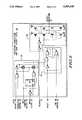
- FIG. 4illustrates one implementation of the resolution selection logic 36.
- the resolution control signal 26determines whether input clock 20 is input to counter stage 0 circuit 40a across STAGE 0 IN signal 46 or whether input clock 20 is input to counter stage 1 circuit 40b across STAGE 1 IN signal 48. If input clock 20 is being input to counter stage 0 circuit 40a, then STAGE 0 OUT signal 50, which is the output of counter stage 0 circuit 40a, is fed into the input of counter stage 1 circuit 40b across STAGE 1 IN signal 48. If input clock 20 is being input to counter stage 1 circuit 40b, then counter stage 0 circuit 40a, STAGE 0 IN signal 46, and STAGE 0 OUT signal 50 are not used.
- FIG. 5illustrates one implementation of the waveform completion and edge adjustment logic 38.
- the circuitry of waveform completion and edge adjustment logic 38can be functionally divided into three sub-blocks.
- the first sub-blockis edge adjust logic 60.
- Edge adjust logic 60receives four signals as inputs, namely edge adjust 44, resolution control 26, duty compare match 42, and input clock 20. These four input signals are used to determine whether output waveform 22 should be inverted, and if so, whether the inversion of output waveform 22 should be delayed by one-half of the input clock 20 period. Output waveform 22 is inverted when duty compare match 42 indicates that there has been a match. The inversion of the output waveform 22 is only delayed if the resolution control signal 26 indicates that the counter 34 is counting by two, and the edge adjust signal 44 indicates that the duty control 24 value is "odd" rather than "even”. If a delay is required, edge adjust logic 60 generates that delay.
- the second sub-blockis polarity determination logic 62.
- This sub-blockis optional.
- Polarity determination logic 62merely determines whether the initial state of output waveform 22 is high or low.
- the duty cycle of a waveformis the percentage of time that the waveform is high during the total waveform period.
- Polarity determination logic 62allows the user to define the duty cycle of output waveform 22 as either the percentage of high time or the percentage of low time, depending upon whether the initial state of output waveform 22 is chosen to be high or low. This is useful because different peripheral devices which receive and use output waveform 22 require different polarities. Some peripheral devices require the initial state of output waveform 22 to be high, and some devices require the initial state to be low.
- the third sub-blockis reset and end of period determination logic 64.
- the reset portion of this circuitryis optional.
- the reset 30 input to this sub-blockmerely forces the value of the output waveform 22 to a particular reset state.
- the reset 30 signalcould be a control signal for disabling output waveform 22 or for performing some other function which required the output to be forced to a known state. In the present embodiment, whether the reset state of output waveform 22 is high or low is defined by the polarity determination logic 62.
- the remaining circuitry in the reset and end of period determination logic 64causes output waveform 22 to be inverted when the end of the period of output waveform 22 has been reached.
- Counter 34asserts the end of period signal 52 when counter 34 reaches its maximum count value and rolls over to its lowest count value.
- the end of period signal 52is received by the reset and end of period determination logic 64 and is used to indicate that the end of the period of output waveform 22 has been reached and that the logic state of output waveform 22 should once again be inverted.
- the above specificationdescribes a data processing system 10 having a high resolution counter module 16 which has improved pulse width resolution.
- the pulse width resolution period (PWRP)can be improved by the predetermined power of two.
- the pulse width resolution period (PWRP)can be reduced by one-half which is a doubling of performance.
- the data processing system 10may or may not be contained on a single semiconductor chip.
- data processor 12may be contained on a semiconductor chip and clock generator 14 may be an oscillator that is not contained on that same semiconductor chip.
- the high resolution counter module 16may be part of a timer or serial subsystem 18 within data processing system 10.
- Various frequencies of input clock 20could be used, with the maximum frequency determined by the limitations of the circuitry.
- the number of stages in counter 34may be any number.
- counter 34may be a down counter that decrements rather than increments, and thus counter 34 counts down until it rolls over from its minimum count value to its maximum count value.
- output waveform 22could be made for all "even” duty control 24 values rather than for all "odd” duty control 24 values.
- output waveform 22could be shortened by one-half input clock 20 period for all "even” values. In order to be able to shorten output waveform 22, there must be a delay in the actual inversion of output waveform 22 in order to allow for any shortening of output waveform 22 that is required.
Landscapes
- Engineering & Computer Science (AREA)
- Theoretical Computer Science (AREA)
- Physics & Mathematics (AREA)
- General Engineering & Computer Science (AREA)
- General Physics & Mathematics (AREA)
- Pulse Circuits (AREA)
Abstract
Description
Claims (20)
Priority Applications (3)
| Application Number | Priority Date | Filing Date | Title |
|---|---|---|---|
| US07/787,167US5293628A (en) | 1991-11-04 | 1991-11-04 | Data processing system which generates a waveform with improved pulse width resolution |
| JP4305863AJPH05259839A (en) | 1991-11-04 | 1992-10-21 | Data processing system generating waveform with improved pulse width resolution and its method |
| EP19920118085EP0540949A3 (en) | 1991-11-04 | 1992-10-22 | A data processing system which generates a waveform with improved pulse width resolution |
Applications Claiming Priority (1)
| Application Number | Priority Date | Filing Date | Title |
|---|---|---|---|
| US07/787,167US5293628A (en) | 1991-11-04 | 1991-11-04 | Data processing system which generates a waveform with improved pulse width resolution |
Publications (1)
| Publication Number | Publication Date |
|---|---|
| US5293628Atrue US5293628A (en) | 1994-03-08 |
Family
ID=25140617
Family Applications (1)
| Application Number | Title | Priority Date | Filing Date |
|---|---|---|---|
| US07/787,167Expired - LifetimeUS5293628A (en) | 1991-11-04 | 1991-11-04 | Data processing system which generates a waveform with improved pulse width resolution |
Country Status (3)
| Country | Link |
|---|---|
| US (1) | US5293628A (en) |
| EP (1) | EP0540949A3 (en) |
| JP (1) | JPH05259839A (en) |
Cited By (20)
| Publication number | Priority date | Publication date | Assignee | Title |
|---|---|---|---|---|
| US5481230A (en)* | 1994-11-14 | 1996-01-02 | Tektronix, Inc. | Phase modulator having individually placed edges |
| US5627500A (en)* | 1995-12-26 | 1997-05-06 | Tektronix, Inc. | Phase modulator having individually placed edges |
| US5734877A (en)* | 1992-09-09 | 1998-03-31 | Silicon Graphics, Inc. | Processor chip having on-chip circuitry for generating a programmable external clock signal and for controlling data patterns |
| US5812831A (en)* | 1996-04-22 | 1998-09-22 | Motorola, Inc. | Method and apparatus for pulse width modulation |
| US5854985A (en)* | 1993-12-15 | 1998-12-29 | Spectrum Information Technologies, Inc. | Adaptive omni-modal radio apparatus and methods |
| US5944835A (en)* | 1996-05-31 | 1999-08-31 | Sgs-Thomson Microelectronics S.A. | Method and programmable device for generating variable width pulses |
| US6138047A (en)* | 1998-02-09 | 2000-10-24 | Delco Electronics Corporation | Low frequency PWM generation method for a microprocessor-based controller |
| US20030184248A1 (en)* | 2002-03-27 | 2003-10-02 | Brother Kogyo Kabushiki Kaisha | Apparatus and method for controlling an electric motor |
| US20040027167A1 (en)* | 2002-08-07 | 2004-02-12 | Mitsubishi Denki Kabushiki Kaisha | Data transfer device for transferring data between blocks of different clock domains |
| US20040078616A1 (en)* | 2002-10-11 | 2004-04-22 | Renesas Technology Corp. | Microcomputer |
| US6934558B1 (en) | 1993-12-15 | 2005-08-23 | Mlr, Llc | Adaptive omni-modal radio apparatus and methods |
| US20060222089A1 (en)* | 2005-04-01 | 2006-10-05 | John Dicky | System for multiplexing independent signals |
| US20080077896A1 (en)* | 2006-09-26 | 2008-03-27 | Fujitsu Limited | Method and apparatus for editing timing diagram, and computer product |
| US20080214231A1 (en)* | 2000-03-22 | 2008-09-04 | Mlr, Llc | Tiered Wireless, Multi-Modal Access System and Method |
| US20100214082A1 (en)* | 2009-02-20 | 2010-08-26 | Redwood Systems, Inc. | Transmission of power and data with frequency modulation |
| US20100213759A1 (en)* | 2009-02-20 | 2010-08-26 | Redwood Systems, Inc. | Digital switch communication |
| US20100237695A1 (en)* | 2009-02-20 | 2010-09-23 | Redwood Systems, Inc. | Smart power device |
| US20100289343A1 (en)* | 2009-05-14 | 2010-11-18 | Redwood Systems, Inc. | Discharge cycle communication |
| USRE42697E1 (en) | 1993-12-15 | 2011-09-13 | Mlr, Llc. | Apparatus and methods for networking omni-modal radio devices |
| EP3764251A3 (en)* | 2019-07-11 | 2021-01-27 | STMicroelectronics (Research & Development) Limited | Time domain discrete transform computation |
Citations (18)
| Publication number | Priority date | Publication date | Assignee | Title |
|---|---|---|---|---|
| FR2342585A1 (en)* | 1976-02-28 | 1977-09-23 | Itt | Polyphase MOSFET circuit for pulse duration variations - uses ring counters with decoders connected to RS flip flop controlled by digital signal applied to AND gates |
| US4191998A (en)* | 1978-03-29 | 1980-03-04 | Honeywell Inc. | Variable symmetry multiphase clock generator |
| JPS5847325A (en)* | 1981-09-17 | 1983-03-19 | Sanyo Electric Co Ltd | Modulating circuit of pulse width |
| US4435757A (en)* | 1979-07-25 | 1984-03-06 | The Singer Company | Clock control for digital computer |
| DE3302744A1 (en)* | 1983-01-27 | 1984-08-02 | Siemens AG, 1000 Berlin und 8000 München | Clocked pulse generator |
| US4546269A (en)* | 1983-12-01 | 1985-10-08 | Control Data Corporation | Method and apparatus for optimally tuning clock signals for digital computers |
| US4564953A (en)* | 1983-03-28 | 1986-01-14 | Texas Instruments Incorporated | Programmable timing system |
| US4618968A (en)* | 1983-11-04 | 1986-10-21 | Motorola, Inc. | Output compare system and method automatically controlilng multiple outputs in a data processor |
| US4754163A (en)* | 1983-07-08 | 1988-06-28 | Hewlett-Packard Company | Pulse generator with adjustable pulse frequency, pulse width and pulse delay |
| WO1988007289A1 (en)* | 1987-03-09 | 1988-09-22 | Hughes Aircraft Company | Method and apparatus for obtaining high frequency resolution of a low frequency signal |
| US4870665A (en)* | 1988-08-04 | 1989-09-26 | Gte Government Systems Corporation | Digital pulse generator having a programmable pulse width and a pulse repetition interval |
| US4881040A (en)* | 1988-08-04 | 1989-11-14 | Gte Government Systems Corporation | Signal generator for producing accurately timed pulse groupings |
| US4935944A (en)* | 1989-03-20 | 1990-06-19 | Motorola, Inc. | Frequency divider circuit with integer and non-integer divisors |
| US4989223A (en)* | 1988-11-25 | 1991-01-29 | Nec Corporation | Serial clock generating circuit |
| US5029272A (en)* | 1989-11-03 | 1991-07-02 | Motorola, Inc. | Input/output circuit with programmable input sensing time |
| US5039950A (en)* | 1989-07-20 | 1991-08-13 | Eastman Kodak Company | Multiple clock synthesizer |
| US5086387A (en)* | 1986-01-17 | 1992-02-04 | International Business Machines Corporation | Multi-frequency clock generation with low state coincidence upon latching |
| US5223742A (en)* | 1991-08-14 | 1993-06-29 | Schumacher Mark E | Circuit and method for monitoring a pulse width modulated waveform |
- 1991
- 1991-11-04USUS07/787,167patent/US5293628A/ennot_activeExpired - Lifetime
- 1992
- 1992-10-21JPJP4305863Apatent/JPH05259839A/enactivePending
- 1992-10-22EPEP19920118085patent/EP0540949A3/ennot_activeCeased
Patent Citations (18)
| Publication number | Priority date | Publication date | Assignee | Title |
|---|---|---|---|---|
| FR2342585A1 (en)* | 1976-02-28 | 1977-09-23 | Itt | Polyphase MOSFET circuit for pulse duration variations - uses ring counters with decoders connected to RS flip flop controlled by digital signal applied to AND gates |
| US4191998A (en)* | 1978-03-29 | 1980-03-04 | Honeywell Inc. | Variable symmetry multiphase clock generator |
| US4435757A (en)* | 1979-07-25 | 1984-03-06 | The Singer Company | Clock control for digital computer |
| JPS5847325A (en)* | 1981-09-17 | 1983-03-19 | Sanyo Electric Co Ltd | Modulating circuit of pulse width |
| DE3302744A1 (en)* | 1983-01-27 | 1984-08-02 | Siemens AG, 1000 Berlin und 8000 München | Clocked pulse generator |
| US4564953A (en)* | 1983-03-28 | 1986-01-14 | Texas Instruments Incorporated | Programmable timing system |
| US4754163A (en)* | 1983-07-08 | 1988-06-28 | Hewlett-Packard Company | Pulse generator with adjustable pulse frequency, pulse width and pulse delay |
| US4618968A (en)* | 1983-11-04 | 1986-10-21 | Motorola, Inc. | Output compare system and method automatically controlilng multiple outputs in a data processor |
| US4546269A (en)* | 1983-12-01 | 1985-10-08 | Control Data Corporation | Method and apparatus for optimally tuning clock signals for digital computers |
| US5086387A (en)* | 1986-01-17 | 1992-02-04 | International Business Machines Corporation | Multi-frequency clock generation with low state coincidence upon latching |
| WO1988007289A1 (en)* | 1987-03-09 | 1988-09-22 | Hughes Aircraft Company | Method and apparatus for obtaining high frequency resolution of a low frequency signal |
| US4870665A (en)* | 1988-08-04 | 1989-09-26 | Gte Government Systems Corporation | Digital pulse generator having a programmable pulse width and a pulse repetition interval |
| US4881040A (en)* | 1988-08-04 | 1989-11-14 | Gte Government Systems Corporation | Signal generator for producing accurately timed pulse groupings |
| US4989223A (en)* | 1988-11-25 | 1991-01-29 | Nec Corporation | Serial clock generating circuit |
| US4935944A (en)* | 1989-03-20 | 1990-06-19 | Motorola, Inc. | Frequency divider circuit with integer and non-integer divisors |
| US5039950A (en)* | 1989-07-20 | 1991-08-13 | Eastman Kodak Company | Multiple clock synthesizer |
| US5029272A (en)* | 1989-11-03 | 1991-07-02 | Motorola, Inc. | Input/output circuit with programmable input sensing time |
| US5223742A (en)* | 1991-08-14 | 1993-06-29 | Schumacher Mark E | Circuit and method for monitoring a pulse width modulated waveform |
Cited By (43)
| Publication number | Priority date | Publication date | Assignee | Title |
|---|---|---|---|---|
| US5734877A (en)* | 1992-09-09 | 1998-03-31 | Silicon Graphics, Inc. | Processor chip having on-chip circuitry for generating a programmable external clock signal and for controlling data patterns |
| US5978926A (en)* | 1992-09-09 | 1999-11-02 | Mips Technologies, Inc. | Processor chip for using an external clock to generate an internal clock and for using data transmit patterns in combination with the internal clock to control transmission of data words to an external memory |
| US6934558B1 (en) | 1993-12-15 | 2005-08-23 | Mlr, Llc | Adaptive omni-modal radio apparatus and methods |
| US5854985A (en)* | 1993-12-15 | 1998-12-29 | Spectrum Information Technologies, Inc. | Adaptive omni-modal radio apparatus and methods |
| US20080274767A1 (en)* | 1993-12-15 | 2008-11-06 | Mlr, Llc | Adaptive Omni-Modal Radio Apparatus and Methods |
| US7386322B2 (en) | 1993-12-15 | 2008-06-10 | Mlr, Llc | Adaptive omni-modal radio apparatus and methods |
| USRE42697E1 (en) | 1993-12-15 | 2011-09-13 | Mlr, Llc. | Apparatus and methods for networking omni-modal radio devices |
| US5481230A (en)* | 1994-11-14 | 1996-01-02 | Tektronix, Inc. | Phase modulator having individually placed edges |
| US5627500A (en)* | 1995-12-26 | 1997-05-06 | Tektronix, Inc. | Phase modulator having individually placed edges |
| US5812831A (en)* | 1996-04-22 | 1998-09-22 | Motorola, Inc. | Method and apparatus for pulse width modulation |
| US5944835A (en)* | 1996-05-31 | 1999-08-31 | Sgs-Thomson Microelectronics S.A. | Method and programmable device for generating variable width pulses |
| US6138047A (en)* | 1998-02-09 | 2000-10-24 | Delco Electronics Corporation | Low frequency PWM generation method for a microprocessor-based controller |
| US8700041B2 (en) | 2000-03-22 | 2014-04-15 | Mlr, Llc | Tiered wireless, multi-modal access system and method |
| US8401559B2 (en) | 2000-03-22 | 2013-03-19 | Mlr, Llc | Tiered wireless, multi-modal access system and method |
| US20080214231A1 (en)* | 2000-03-22 | 2008-09-04 | Mlr, Llc | Tiered Wireless, Multi-Modal Access System and Method |
| US8831617B2 (en) | 2000-03-22 | 2014-09-09 | Mlr, Llc | Tiered wireless, multi-modal access system and method |
| US9532267B2 (en) | 2000-03-22 | 2016-12-27 | Mobile Data Off-Loading Inc. | Tiered wireless, multi-modal access system and method |
| US8078221B2 (en) | 2000-03-22 | 2011-12-13 | Mlr, Llc | Tiered wireless, multi-modal access system and method |
| US7627340B2 (en) | 2000-03-22 | 2009-12-01 | Mlr, Llc | Tiered wireless, multi-modal access system and method |
| US10098047B2 (en) | 2000-03-22 | 2018-10-09 | Mobile Data Off-Loading, Inc. | Tiered wireless, multi-modal access system and method |
| US20030184248A1 (en)* | 2002-03-27 | 2003-10-02 | Brother Kogyo Kabushiki Kaisha | Apparatus and method for controlling an electric motor |
| US7230401B2 (en)* | 2002-03-27 | 2007-06-12 | Brother Kogyo Kabushiki Kaisha | Apparatus and method for controlling an electric motor |
| US6911843B2 (en)* | 2002-08-07 | 2005-06-28 | Renesas Technology Corp. | Data transfer device for transferring data between blocks of different clock domains |
| US20040027167A1 (en)* | 2002-08-07 | 2004-02-12 | Mitsubishi Denki Kabushiki Kaisha | Data transfer device for transferring data between blocks of different clock domains |
| US7290126B2 (en)* | 2002-10-11 | 2007-10-30 | Renesas Technology Corp. | One-chip microcomputer with multiple timers |
| US20040078616A1 (en)* | 2002-10-11 | 2004-04-22 | Renesas Technology Corp. | Microcomputer |
| US7551669B2 (en) | 2005-04-01 | 2009-06-23 | Harman International Industries, Incorporated | System for multiplexing independent signals |
| US20060222089A1 (en)* | 2005-04-01 | 2006-10-05 | John Dicky | System for multiplexing independent signals |
| US7911466B2 (en)* | 2006-09-26 | 2011-03-22 | Fujitsu Limited | Method and apparatus for editing timing diagram, and computer product |
| US20080077896A1 (en)* | 2006-09-26 | 2008-03-27 | Fujitsu Limited | Method and apparatus for editing timing diagram, and computer product |
| US8248230B2 (en) | 2009-02-20 | 2012-08-21 | Redwood Systems, Inc. | Smart power device |
| US8207635B2 (en) | 2009-02-20 | 2012-06-26 | Redwood Systems, Inc. | Digital switch communication |
| US8390441B2 (en) | 2009-02-20 | 2013-03-05 | Redwood Systems, Inc. | Smart power device |
| US20100237695A1 (en)* | 2009-02-20 | 2010-09-23 | Redwood Systems, Inc. | Smart power device |
| US8427300B2 (en) | 2009-02-20 | 2013-04-23 | Redwood Systems, Inc. | Transmission of power and data with frequency modulation |
| US20100213759A1 (en)* | 2009-02-20 | 2010-08-26 | Redwood Systems, Inc. | Digital switch communication |
| US20100214082A1 (en)* | 2009-02-20 | 2010-08-26 | Redwood Systems, Inc. | Transmission of power and data with frequency modulation |
| US8890679B2 (en) | 2009-02-20 | 2014-11-18 | Redwood Systems, Inc. | Smart power device |
| US8890663B2 (en) | 2009-02-20 | 2014-11-18 | Redwood Systems, Inc. | Transmission of power and data at multiple power levels |
| US9583979B2 (en) | 2009-02-20 | 2017-02-28 | Redwood Systems, Inc. | Powering a fixture from AC and DC sources |
| US20100289343A1 (en)* | 2009-05-14 | 2010-11-18 | Redwood Systems, Inc. | Discharge cycle communication |
| US8058750B2 (en) | 2009-05-14 | 2011-11-15 | Redwood Systems, Inc. | Discharge cycle communication |
| EP3764251A3 (en)* | 2019-07-11 | 2021-01-27 | STMicroelectronics (Research & Development) Limited | Time domain discrete transform computation |
Also Published As
| Publication number | Publication date |
|---|---|
| JPH05259839A (en) | 1993-10-08 |
| EP0540949A2 (en) | 1993-05-12 |
| EP0540949A3 (en) | 1993-07-07 |
Similar Documents
| Publication | Publication Date | Title |
|---|---|---|
| US5293628A (en) | Data processing system which generates a waveform with improved pulse width resolution | |
| CA1198780A (en) | Self-clocking binary receiver | |
| US4799022A (en) | Frequency doubler with duty cycle monitor means | |
| US6169889B1 (en) | Method and electronic device using random pulse characteristics in digital signals | |
| KR0139764B1 (en) | Pulse generator | |
| JP2549229B2 (en) | Digital clock signal waveform shaping circuit | |
| US4837721A (en) | Digital divider with integer and fractional division capability | |
| JP2004013784A (en) | Clock-modulating circuit | |
| US5854755A (en) | Clock frequency multiplication device | |
| JP2678115B2 (en) | Timer circuit | |
| US6337588B1 (en) | Apparatus and method for doubling the frequency of a clock signal | |
| JP3649874B2 (en) | Frequency divider circuit | |
| US4862096A (en) | Programmable multiphase sequence controller | |
| US6204711B1 (en) | Reduced error asynchronous clock | |
| JP2906966B2 (en) | Pulse switching circuit | |
| JPH11509658A (en) | Extended chip select reset device and method | |
| US6901528B2 (en) | Minimum latency propagation of variable pulse width signals across clock domains with variable frequencies | |
| KR100236083B1 (en) | Pulse generator | |
| JP3284317B2 (en) | Pulse width modulator | |
| KR100563244B1 (en) | Variable period and assertion width req/ack pulse generator for synchronous scsi data transfers | |
| JPH0879029A (en) | Four-phase clock pulse generating circuit | |
| KR0183948B1 (en) | Frequency multiplication circuit | |
| JP2529401B2 (en) | Timing signal generation circuit | |
| KR970008366B1 (en) | Stepping Motor Control Circuit | |
| KR0150682B1 (en) | Clock multiplier |
Legal Events
| Date | Code | Title | Description |
|---|---|---|---|
| AS | Assignment | Owner name:MOTOROLA, INC.,, ILLINOIS Free format text:ASSIGNMENT OF ASSIGNORS INTEREST.;ASSIGNORS:LANGAN, JOHN A.;AMEDEO, ROBERT J.;FRONTERA, ROBERTO M.;REEL/FRAME:005918/0575 Effective date:19911031 | |
| STCF | Information on status: patent grant | Free format text:PATENTED CASE | |
| CC | Certificate of correction | ||
| FPAY | Fee payment | Year of fee payment:4 | |
| FPAY | Fee payment | Year of fee payment:8 | |
| AS | Assignment | Owner name:FREESCALE SEMICONDUCTOR, INC., TEXAS Free format text:ASSIGNMENT OF ASSIGNORS INTEREST;ASSIGNOR:MOTOROLA, INC.;REEL/FRAME:015698/0657 Effective date:20040404 Owner name:FREESCALE SEMICONDUCTOR, INC.,TEXAS Free format text:ASSIGNMENT OF ASSIGNORS INTEREST;ASSIGNOR:MOTOROLA, INC.;REEL/FRAME:015698/0657 Effective date:20040404 | |
| FPAY | Fee payment | Year of fee payment:12 | |
| AS | Assignment | Owner name:CITIBANK, N.A. AS COLLATERAL AGENT, NEW YORK Free format text:SECURITY AGREEMENT;ASSIGNORS:FREESCALE SEMICONDUCTOR, INC.;FREESCALE ACQUISITION CORPORATION;FREESCALE ACQUISITION HOLDINGS CORP.;AND OTHERS;REEL/FRAME:018855/0129 Effective date:20061201 Owner name:CITIBANK, N.A. AS COLLATERAL AGENT,NEW YORK Free format text:SECURITY AGREEMENT;ASSIGNORS:FREESCALE SEMICONDUCTOR, INC.;FREESCALE ACQUISITION CORPORATION;FREESCALE ACQUISITION HOLDINGS CORP.;AND OTHERS;REEL/FRAME:018855/0129 Effective date:20061201 | |
| AS | Assignment | Owner name:CITIBANK, N.A., AS COLLATERAL AGENT,NEW YORK Free format text:SECURITY AGREEMENT;ASSIGNOR:FREESCALE SEMICONDUCTOR, INC.;REEL/FRAME:024397/0001 Effective date:20100413 Owner name:CITIBANK, N.A., AS COLLATERAL AGENT, NEW YORK Free format text:SECURITY AGREEMENT;ASSIGNOR:FREESCALE SEMICONDUCTOR, INC.;REEL/FRAME:024397/0001 Effective date:20100413 | |
| AS | Assignment | Owner name:FREESCALE SEMICONDUCTOR, INC., TEXAS Free format text:PATENT RELEASE;ASSIGNOR:CITIBANK, N.A., AS COLLATERAL AGENT;REEL/FRAME:037356/0553 Effective date:20151207 Owner name:FREESCALE SEMICONDUCTOR, INC., TEXAS Free format text:PATENT RELEASE;ASSIGNOR:CITIBANK, N.A., AS COLLATERAL AGENT;REEL/FRAME:037356/0143 Effective date:20151207 Owner name:FREESCALE SEMICONDUCTOR, INC., TEXAS Free format text:PATENT RELEASE;ASSIGNOR:CITIBANK, N.A., AS COLLATERAL AGENT;REEL/FRAME:037354/0225 Effective date:20151207 |