US5293528A - Electrophoretic display panel and associated methods providing single pixel erase capability - Google Patents
Electrophoretic display panel and associated methods providing single pixel erase capabilityDownload PDFInfo
- Publication number
- US5293528A US5293528AUS07/841,380US84138092AUS5293528AUS 5293528 AUS5293528 AUS 5293528AUS 84138092 AUS84138092 AUS 84138092AUS 5293528 AUS5293528 AUS 5293528A
- Authority
- US
- United States
- Prior art keywords
- lines
- grid
- anode
- local anode
- cathode
- Prior art date
- Legal status (The legal status is an assumption and is not a legal conclusion. Google has not performed a legal analysis and makes no representation as to the accuracy of the status listed.)
- Expired - Fee Related
Links
- 238000000034methodMethods0.000titleclaimsdescription23
- 239000000049pigmentSubstances0.000claimsdescription33
- 239000002245particleSubstances0.000claimsdescription25
- 239000012530fluidSubstances0.000claimsdescription13
- 239000011159matrix materialSubstances0.000claimsdescription12
- 239000012212insulatorSubstances0.000claimsdescription9
- 238000005381potential energyMethods0.000claimsdescription4
- 239000006185dispersionSubstances0.000claimsdescription3
- 230000006872improvementEffects0.000claimsdescription2
- 230000001939inductive effectEffects0.000claimsdescription2
- 239000004020conductorSubstances0.000description10
- 229920002120photoresistant polymerPolymers0.000description10
- 239000000463materialSubstances0.000description6
- 230000005686electrostatic fieldEffects0.000description5
- 230000006870functionEffects0.000description5
- 239000011148porous materialSubstances0.000description5
- 125000006850spacer groupChemical group0.000description5
- PXHVJJICTQNCMI-UHFFFAOYSA-NNickelChemical compound[Ni]PXHVJJICTQNCMI-UHFFFAOYSA-N0.000description4
- VYPSYNLAJGMNEJ-UHFFFAOYSA-NSilicium dioxideChemical compoundO=[Si]=OVYPSYNLAJGMNEJ-UHFFFAOYSA-N0.000description4
- 229910052751metalInorganic materials0.000description4
- 239000002184metalSubstances0.000description4
- 239000000725suspensionSubstances0.000description4
- 230000005012migrationEffects0.000description3
- 238000013508migrationMethods0.000description3
- VYZAMTAEIAYCRO-UHFFFAOYSA-NChromiumChemical compound[Cr]VYZAMTAEIAYCRO-UHFFFAOYSA-N0.000description2
- 239000004593EpoxySubstances0.000description2
- 230000004888barrier functionEffects0.000description2
- 230000008901benefitEffects0.000description2
- 239000011248coating agentSubstances0.000description2
- 238000000576coating methodMethods0.000description2
- 229910052681coesiteInorganic materials0.000description2
- 238000010276constructionMethods0.000description2
- 229910052906cristobaliteInorganic materials0.000description2
- 230000009977dual effectEffects0.000description2
- 238000005530etchingMethods0.000description2
- 238000010030laminatingMethods0.000description2
- 239000000203mixtureSubstances0.000description2
- 229910052759nickelInorganic materials0.000description2
- 239000000377silicon dioxideSubstances0.000description2
- 235000012239silicon dioxideNutrition0.000description2
- 229910052682stishoviteInorganic materials0.000description2
- 229910052905tridymiteInorganic materials0.000description2
- 230000000007visual effectEffects0.000description2
- 238000012800visualizationMethods0.000description2
- 230000004913activationEffects0.000description1
- 238000004026adhesive bondingMethods0.000description1
- 229910052782aluminiumInorganic materials0.000description1
- XAGFODPZIPBFFR-UHFFFAOYSA-NaluminiumChemical compound[Al]XAGFODPZIPBFFR-UHFFFAOYSA-N0.000description1
- 238000007743anodisingMethods0.000description1
- 230000009286beneficial effectEffects0.000description1
- 238000001816coolingMethods0.000description1
- 230000003247decreasing effectEffects0.000description1
- 238000000151depositionMethods0.000description1
- 230000008021depositionEffects0.000description1
- 238000010586diagramMethods0.000description1
- -1e.g.Substances0.000description1
- 230000000694effectsEffects0.000description1
- 239000005357flat glassSubstances0.000description1
- 239000011521glassSubstances0.000description1
- 238000010348incorporationMethods0.000description1
- AMGQUBHHOARCQH-UHFFFAOYSA-Nindium;oxotinChemical compound[In].[Sn]=OAMGQUBHHOARCQH-UHFFFAOYSA-N0.000description1
- 238000009413insulationMethods0.000description1
- 238000003475laminationMethods0.000description1
- 230000000873masking effectEffects0.000description1
- 230000004048modificationEffects0.000description1
- 238000012986modificationMethods0.000description1
- 238000007747platingMethods0.000description1
- 230000008569processEffects0.000description1
- 230000009467reductionEffects0.000description1
- 230000004044responseEffects0.000description1
- 239000004065semiconductorSubstances0.000description1
- 239000007787solidSubstances0.000description1
- 238000004544sputter depositionMethods0.000description1
- 229910001220stainless steelInorganic materials0.000description1
- 239000010935stainless steelSubstances0.000description1
Images


Classifications
- G—PHYSICS
- G09—EDUCATION; CRYPTOGRAPHY; DISPLAY; ADVERTISING; SEALS
- G09G—ARRANGEMENTS OR CIRCUITS FOR CONTROL OF INDICATING DEVICES USING STATIC MEANS TO PRESENT VARIABLE INFORMATION
- G09G3/00—Control arrangements or circuits, of interest only in connection with visual indicators other than cathode-ray tubes
- G09G3/20—Control arrangements or circuits, of interest only in connection with visual indicators other than cathode-ray tubes for presentation of an assembly of a number of characters, e.g. a page, by composing the assembly by combination of individual elements arranged in a matrix no fixed position being assigned to or needed to be assigned to the individual characters or partial characters
- G09G3/34—Control arrangements or circuits, of interest only in connection with visual indicators other than cathode-ray tubes for presentation of an assembly of a number of characters, e.g. a page, by composing the assembly by combination of individual elements arranged in a matrix no fixed position being assigned to or needed to be assigned to the individual characters or partial characters by control of light from an independent source
- G09G3/3433—Control arrangements or circuits, of interest only in connection with visual indicators other than cathode-ray tubes for presentation of an assembly of a number of characters, e.g. a page, by composing the assembly by combination of individual elements arranged in a matrix no fixed position being assigned to or needed to be assigned to the individual characters or partial characters by control of light from an independent source using light modulating elements actuated by an electric field and being other than liquid crystal devices and electrochromic devices
- G09G3/344—Control arrangements or circuits, of interest only in connection with visual indicators other than cathode-ray tubes for presentation of an assembly of a number of characters, e.g. a page, by composing the assembly by combination of individual elements arranged in a matrix no fixed position being assigned to or needed to be assigned to the individual characters or partial characters by control of light from an independent source using light modulating elements actuated by an electric field and being other than liquid crystal devices and electrochromic devices based on particles moving in a fluid or in a gas, e.g. electrophoretic devices
- G09G3/3446—Control arrangements or circuits, of interest only in connection with visual indicators other than cathode-ray tubes for presentation of an assembly of a number of characters, e.g. a page, by composing the assembly by combination of individual elements arranged in a matrix no fixed position being assigned to or needed to be assigned to the individual characters or partial characters by control of light from an independent source using light modulating elements actuated by an electric field and being other than liquid crystal devices and electrochromic devices based on particles moving in a fluid or in a gas, e.g. electrophoretic devices with more than two electrodes controlling the modulating element
- G—PHYSICS
- G02—OPTICS
- G02F—OPTICAL DEVICES OR ARRANGEMENTS FOR THE CONTROL OF LIGHT BY MODIFICATION OF THE OPTICAL PROPERTIES OF THE MEDIA OF THE ELEMENTS INVOLVED THEREIN; NON-LINEAR OPTICS; FREQUENCY-CHANGING OF LIGHT; OPTICAL LOGIC ELEMENTS; OPTICAL ANALOGUE/DIGITAL CONVERTERS
- G02F1/00—Devices or arrangements for the control of the intensity, colour, phase, polarisation or direction of light arriving from an independent light source, e.g. switching, gating or modulating; Non-linear optics
- G02F1/01—Devices or arrangements for the control of the intensity, colour, phase, polarisation or direction of light arriving from an independent light source, e.g. switching, gating or modulating; Non-linear optics for the control of the intensity, phase, polarisation or colour
- G02F1/165—Devices or arrangements for the control of the intensity, colour, phase, polarisation or direction of light arriving from an independent light source, e.g. switching, gating or modulating; Non-linear optics for the control of the intensity, phase, polarisation or colour based on translational movement of particles in a fluid under the influence of an applied field
- G02F1/166—Devices or arrangements for the control of the intensity, colour, phase, polarisation or direction of light arriving from an independent light source, e.g. switching, gating or modulating; Non-linear optics for the control of the intensity, phase, polarisation or colour based on translational movement of particles in a fluid under the influence of an applied field characterised by the electro-optical or magneto-optical effect
- G02F1/167—Devices or arrangements for the control of the intensity, colour, phase, polarisation or direction of light arriving from an independent light source, e.g. switching, gating or modulating; Non-linear optics for the control of the intensity, phase, polarisation or colour based on translational movement of particles in a fluid under the influence of an applied field characterised by the electro-optical or magneto-optical effect by electrophoresis
- G—PHYSICS
- G02—OPTICS
- G02F—OPTICAL DEVICES OR ARRANGEMENTS FOR THE CONTROL OF LIGHT BY MODIFICATION OF THE OPTICAL PROPERTIES OF THE MEDIA OF THE ELEMENTS INVOLVED THEREIN; NON-LINEAR OPTICS; FREQUENCY-CHANGING OF LIGHT; OPTICAL LOGIC ELEMENTS; OPTICAL ANALOGUE/DIGITAL CONVERTERS
- G02F1/00—Devices or arrangements for the control of the intensity, colour, phase, polarisation or direction of light arriving from an independent light source, e.g. switching, gating or modulating; Non-linear optics
- G02F1/01—Devices or arrangements for the control of the intensity, colour, phase, polarisation or direction of light arriving from an independent light source, e.g. switching, gating or modulating; Non-linear optics for the control of the intensity, phase, polarisation or colour
- G02F1/165—Devices or arrangements for the control of the intensity, colour, phase, polarisation or direction of light arriving from an independent light source, e.g. switching, gating or modulating; Non-linear optics for the control of the intensity, phase, polarisation or colour based on translational movement of particles in a fluid under the influence of an applied field
- G02F1/1675—Constructional details
- G02F1/1679—Gaskets; Spacers; Sealing of cells; Filling or closing of cells
- G—PHYSICS
- G09—EDUCATION; CRYPTOGRAPHY; DISPLAY; ADVERTISING; SEALS
- G09G—ARRANGEMENTS OR CIRCUITS FOR CONTROL OF INDICATING DEVICES USING STATIC MEANS TO PRESENT VARIABLE INFORMATION
- G09G2300/00—Aspects of the constitution of display devices
- G09G2300/06—Passive matrix structure, i.e. with direct application of both column and row voltages to the light emitting or modulating elements, other than LCD or OLED
- G—PHYSICS
- G09—EDUCATION; CRYPTOGRAPHY; DISPLAY; ADVERTISING; SEALS
- G09G—ARRANGEMENTS OR CIRCUITS FOR CONTROL OF INDICATING DEVICES USING STATIC MEANS TO PRESENT VARIABLE INFORMATION
- G09G2330/00—Aspects of power supply; Aspects of display protection and defect management
- G09G2330/02—Details of power systems and of start or stop of display operation
Landscapes
- Physics & Mathematics (AREA)
- Nonlinear Science (AREA)
- General Physics & Mathematics (AREA)
- Optics & Photonics (AREA)
- Engineering & Computer Science (AREA)
- Computer Hardware Design (AREA)
- Theoretical Computer Science (AREA)
- Health & Medical Sciences (AREA)
- Life Sciences & Earth Sciences (AREA)
- Chemical & Material Sciences (AREA)
- Chemical Kinetics & Catalysis (AREA)
- Electrochemistry (AREA)
- Molecular Biology (AREA)
- Electrochromic Elements, Electrophoresis, Or Variable Reflection Or Absorption Elements (AREA)
- Control Of Indicators Other Than Cathode Ray Tubes (AREA)
- Devices For Indicating Variable Information By Combining Individual Elements (AREA)
Abstract
Description
The present invention relates to an electrophoretic display panel apparatus and methods of operation and, more particularly, to multi-electrode electrophoretic display panels which permit pixel erasure.
Electrophoretic displays (EPIDS) are now well known. A variety of display types and features are taught in several patents issued in the names of the inventors herein, Frank J. DiSanto and Denis A. Krusos and assigned to the assignee herein, Copytele, Inc. of Huntington Station, N.Y. For example, U.S. Pat. Nos. 4,655,897 and 4,732,830, each entitled ELECTROPHORETIC DISPLAY PANELS AND ASSOCIATED METHODS describe the basic operation and construction of an electrophoretic display. U.S. Pat. No. 4,742,345, entitled ELECTROPHORETIC DISPLAY PANELS AND METHODS THEREFOR, describes a display having improved alignment and contrast. Many other patents regarding such displays are also assigned to Copytele, Inc. The following issued patents and pending applications by the inventors herein and assigned to CopyTele, Inc. and which may have some relevance to the present invention are: application Ser. No. 07/794,969, filed Nov. 20, 1991, entitled ELECTROPHORETIC DISPLAY PANEL WITH INTERNAL MESH BACKGROUND SCREEN; DUAL ANODE FLAT PANEL ELECTROPHORETIC DISPLAY APPARATUS, U.S. Pat. No. 5,053,763, issued Oct. 1, 1991; ELECTROPHORETIC DISPLAY WITH SELECTIVE LINE ERASURE, U.S. Pat. No. 5,066,946 issued Nov. 19, 1991; SEMITRANSPARENTELECTROPHORETIC INFORMATION DISPLAYS (EPID) EMPLOYING MESH LIKE ELECTRODES, U.S. Pat. No. 5,041,824 issued on Aug. 20, 1991; application Ser. No. 752,184 filed on Aug. 23, 1991 entitled ELECTROPHORETIC DISPLAY WITH SINGLE CHARACTER ERASURE, which is a continuation of Ser. No. 699,216 filed on May 13, 1991 having the same title; application Ser. No. 07/667,630, filed Mar. 11, 1991, entitled ELECTROPHORETIC DISPLAY PANEL WITH PLURAL ELECTRICALLY INDEPENDENT ANODE ELEMENTS, each of which are indicated below.
The display panels shown in the above-mentioned patents operate upon the same basic principle, viz., if a suspension of electrically charged pigment particles in a dielectric fluid is subjected to an applied electrostatic field, the pigment particles will migrate through the fluid in response to the electrostatic field. Given a substantially homogeneous suspension of particles having a pigment color different from that of the dielectric fluid, if the applied electrostatic field is localized it will cause a visually observable localized pigment particle migration. The localized pigment particle migration results either in a localized area of concentration or rarefaction of particles depending upon the sign and direction of the electrostatic field and the charge on the pigment particles. Certain of the electrophoretic display apparatus taught in such issued Patents are "triode-type" displays having a plurality of independent, parallel, cathode row conductor members deposited in the horizontal with transverse grid lines insulated from the anode lines. The grid and cathode lines form an X-Y matrix which can be accessed to address and control the pigment particles according to a selected X-Y intersection or pixel. U.S. Pat. No. 5,041,024 depicts a "tetrode" type display including a mesh electrode located between the anode and the X-Y grid cathode matrix. The operating voltages on both of the cathode and grid must be able to assume at least two states corresponding to a logical one and a logical zero. Logical one for the cathode may either correspond to attraction or repulsion of pigment. Typically, the cathode and grid voltages are selected such that only when both are a logical one at a particular intersection point, will a sufficient electrostatic field be present at the intersection relative to the anode to cause the writing of a visual bit of information on the display through migration of pigment particles. The bit may be erased, e.g., upon a reversal of polarity and a logical zero-zero state occurring at the intersection coordinated with an erase voltage gradient between anode and cathode. In this manner, digitized data can be displayed on the electrophoretic display.
An alternative EPID construction is described in U.S. Pat. No. 5,053,763, referred to above, which relates to an electrophoretic display in which the cathode/grid matrix as is found in triode-type displays is overlayed by a plurality of independent separately addressable "local" anode lines to constitute a "tetrode". The local anode lines are deposited upon and align with the grid lines and are insulated therefrom by interstitial lines of photoresist. The local anode lines may be in addition to a "remote" anode, which is a layer deposited upon the anode faceplate as in triode displays. The dual anode structure aforesaid provides enhanced operation by eliminating unwanted variations in display brightness between frames, increasing the speed of the display and decreasing the anode voltage required during Write and Hold cycles, all as explained in application Ser. No. 07/345,825, which is incorporated herein by reference.
In yet another form of EPID, as described in application Ser. No. 07/667,630, a triode is formed by a plurality of independent anode elements deposited upon one faceplate and a plurality of independent cathode elements deposited at right angles thereto on an opposing faceplate. An electrically continuous grid with a plurality of pores therein is deposited upon a layer of insulation overlying the cathode lines and is intermediate the cathode and anode lines.
To be useful as a display, an electrophoretic display must be able to assume a blank or erased state; must be able to display character data written during a write operation; and must be able to continually maintain or hold the written characters (and blank characters) in a hold mode until they are erased or overwritten. These three modes of operation, i.e., erase, write and hold are well documented in existing patents issued to the inventors herein and such description shall not be repeated at length herein. The above-described patents and pending patent applications provide apparatus and methods for hold, full write (all pixels written), full erase (all pixels erased), selective write (writing selective pixels in previously erased positions), selective character line erasure and selective character erasure. As one can ascertain, a character is generated by the activation or writing in of a plurality of pixels, each of which can form or provide part of the character. It is therefore an object of the present invention to provide a method for operating an electrophoretic display with an internal mesh element to allow single pixel erasure, thereby simultaneously realizing the advantages and benefits of a display of this type, as well as, the desired discrete erasure function.
The problems and disadvantages associated with pixel display control in conventional electrophoretic displays are overcome by the present invention which includes in a tetrode-type electrophoretic display of the type having a plurality of parallel cathode lines arranged in a given direction, a plurality of parallel grid lines insulated from the cathode lines and perpendicular thereto to form an X-Y addressing matrix, a plurality of local anode lines deposited upon the grid lines and insulated therefrom by insulator strips, a remote anode separated from the local anode lines with the space therebetween accommodating an electrophoretic dispersion including pigment particles suspended in a fluid and an electrically conductive screen allowing the pigment particles to pass therethrough, the improvement of disposing the local anode lines perpendicular to the grid lines. In a method of operating the display the cathode lines, the grid lines, the screen, the local anode lines and the remote anode are electrically connected to a source of electrical potential energy. The source simultaneously provides a selected set of independent voltages to each of the cathode lines, the grid lines, the screen, the local anode lines and the remote anode under the control of a controller for controlling the independent voltages supplied by the source. By controlling the source of electrical potential energy, voltage levels are applied to the cathode matrix, the grid matrix, the screen, the local anode lines and the remote anode to selectively write and erase single pixels on the display.
For a better understanding of the present invention, reference is made to the following detailed description of an exemplary embodiment considered in conjunction with the accompanying drawings, in which:
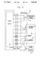
FIG. 1 is an exploded perspective view of an electrophoretic display in accordance with an exemplary embodiment of the present invention.
FIG. 2 is a cross-sectional view of the electrophoretic display shown in FIG. 1 in the unexploded state, taken along section line II--II and looking in the direction of the arrows.
FIG. 3 is a plan view of a local anode line of the display having a tined configuration.
FIG. 4 is a schematic diagram showing the connection of the devices depicted in FIGS. 1 and 2 to a power supply as controlled by a controller.
FIG. 1 shows anelectrophoretic display 10 in accordance with the present invention. Thedisplay 10 has ananode faceplate 12 and acathode faceplate 14 which are sealably affixed on either side ofintermediate spaces faceplates
In the invention, as depicted in FIG. 1, for example, a plurality of independent, electrically conductive cathode members 18 (horizontal rows) are deposited upon thecathode faceplate 14 using conventional deposition and etching techniques. It is preferred that thecathode members 18 be composed of Indium Tin Oxide (ITO) as set forth in U.S. Pat. No. 4,742,345. A plurality of independentgrid conductor members 20 are superimposed in the vertical over thecathode members 18 and are insulated therefrom by an interstitial photoresist layer 22 (see FIG. 2). Thegrid members 20 may be formed by coating thephotoresist layer 22 with a metal, such as nickel, using sputtering techniques or the like, and then selectively masking and etching to yield the intersecting but insulated configuration shown in FIGS. 1 and 2. Each cathode andgrid member contact pad 24 or is otherwise adapted to permit connection to display driver circuitry (not shown).
As can be appreciated from FIG. 1, the overlaying ofgrid lines 20 uponcathode lines 18 creates a plurality of wells 21 bounded by the intersectinglines grid 20 andcathode 18 lines in a tyned configuration. The wells 21 communicate with the fluid contained within the EPID and thus permit pigment particles to travel close to theglass cathode faceplate 14 where they are most clearly visible.
Ananode 26 is formed on an interior surface of theanode faceplate 12 by plating with a thin layer of conductor material, such as, chrome. A mesh element orscreen 28 is sandwiched betweenspacers EPID 10. Themesh screen 28 has a plurality ofpores 29 through which pigment particles may pass so as not to obstruct the normal operation of the EPID. Coincidental to the light barrier function, the mesh itself is an optically significant element, i.e., it is readily visible to the naked eye. It is preferred that the mesh appear as a flat planar object. This is achieved by making the mesh with the minimum pore size which does not critically impede pigment movement. A mesh screen having suitable characteristics is commercially available from the Buckee Mears Co., viz., a perforated stainless steel mesh having an approximate thickness and pore size of 10 to 12 mils. The mesh has an open area ratio, i.e., the ratio of the sum of pore area to the total surface area on one surface of the screen, of approximately 40% to 50%. The mesh is blackened by an anodizing process. The significance of themesh screen 28 is that it provides a solid visual background for the display of pixels and it permits a reduction of dye concentration to effect a desired background intensity. It has also been observed that the above-described mesh screen provides such an effective background that no dye is required. Themesh screen 28 also functions to prevent inadvertent backlighting due to the overall translucence of theEPID 10. It should be observed that thescreen 28 is positioned in theEPID 10 such that when the pigment is in the display position, it is on one side of thescreen 28 and when it is in the written position it is on the other side of thescreen 28, obscured from view by thescreen 28 and/or dye in the solution.
In the present invention, thescreen 28 is fabricated from an electrically conductive material so that it can be utilized to carry an electric charge for the purpose of aiding in controlling the movement of the pigment particles. FIGS. 1 and 2 illustrate the incorporation of themesh screen 28 into a tetrode-type display. The tetrode display includes a plurality oflocal anode elements 32 which are deposited upon corresponding photoresist insulator strips 34 (see FIG. 2) formed perpendicular to thegrid elements 20. The methods for forming thelocal anode elements 32 are set forth at length in application Ser. No. 07/345,825. In brief, a layer of SiO2 is applied over thegrid elements 20, followed by a layer of photoresist. A layer of metal, e.g., nickel or aluminum, is applied over the photoresist layer. Yet another layer of photoresist is applied over the metal layer, and is then masked, exposed and developed perpendicular to the grid elements. The metal layer is then etched with a suitable solution. The photoresist is then plasma etched down to the cathode structure.
To form anEPID 10 like that shown in FIG. 1, the parts may be assembled in a stack and placed in an oven for baking. Thespacers EPID 10 shown, such as, e.g., gluing. The lamination of the EPID elements forms an envelope for containing the dielectric fluid/pigment particle suspension.
The discrete cathode andgrid members electrophoretic display 10 can assume a variety of voltages during operation for controlling the display operations of erase, hold and write at the numerous points of intersection defining a cathode/grid matrix. A display panel would have a large number of intersections, e.g., 2,200×1,700 or a total of 3,740,000 separately addressable intersection points. for ease of illustration, however, only afew cathode members 18 andgrid members 20 are depicted. Similarly, the shape and proportions of the elements depicted are for purposes of illustration only. The dimensions of the respective elements have also been greatly enlarged for illustration and are not necessarily in proportion to an actual operational device. More illustrations of electrophoretic displays, their components and electrical circuitry can be seen by referring to U.S. Pat. Nos. 4,742,345 and 4,772,820, each being awarded to the inventors herein and which are incorporated by reference herein.
Certain details have been omitted from the device depicted, but are taught in prior patents. For example it has been determined that a SiO2 coating on certain of the conductor elements provides beneficial results. See application Ser. No. 07/675,733, filed Mar. 27, 1991 and entitled ELECTROPHORETIC DISPLAY PANEL WITH SEMICONDUCTOR COATED ELEMENTS by the inventors herein and assigned to the assignee herein.
It has previously been shown that certain conductor elements having a tined configuration provide enhanced resolution, see U.S. Pat. No. 4,742,345 issued to the inventors herein and assigned to the present assignee, such patent being incorporated herein by reference. In the present invention, it is preferred that each local anode line have a tined configuration as described more specifically below.
FIG. 2 shows the electrophoretic display of FIG. 1 assembled and in cross-section. Theremote anode 26 in the embodiment shown, is a plate-like area of conductor material having a length and width essentially matching that of the cathode/grid matrix, i.e., coextensive with the matrix, as is taught in the above referenced patents and applications of the present applicant. Thecathode elements 18,grid elements 20 and grid insulator strips 22 as are also like those shown in the foregoing patents, etc. Since all conductor elements are quite thin, they extend beneath theinterstitial spacers epoxy bonding material 30 is depicted providing the laminating bond betweenspacers faceplates mesh screen 28 between thespacers 16a and b.
A tined configuration for thelocal anode lines 32 is depicted in FIG. 3. Each local anode line preferably has fourtines 33 which may, for example be about 16.8 um wide and separated by aspace 35 approximately 15 um wide, each tine rejoining a common electrically continuous portion of the local anode at both terminal ends.
The operation of the display will now be described. For the purposes of illustration, the following may be taken as initial assumptions: (1) negatively surface-charged, light colored pigment particles suspended in a clear or dark dielectric fluid; (2) a darkcolored screen element 28; and (3) visualization of the image at thecathode faceplate 14. Given these initial conditions, a written pixel is represented by the absence of visible pigment particles, hence is a dark pixel. Erased pixels would be represented by visible pigment particles at that location. For example, a totally erased display is completely light colored due to the presence of visible pigment particles at the cathode faceplate. It should be understood that these assumptions are merely exemplary, given that the surface of visualization could be the anode faceplate. Alternatively, the coloration of the particles and the background could be altered, etc., all within the confines of the present invention as described herein.
Since the voltages applied to the various elements of the display for a given function will depend upon the dimensions and distance between elements, the following dimensions can be assumed for the purposes of illustration:
(1)Cathode line 18 width=112 μm.
(2)Cathode line 18 spacing=15 μm.
(3)Photoresist layer 22 thickness=3-4 μm.
(4)Grid line 20 width and composition=112 μm (6 tynes), chrome
(5)Photoresist layer 34 thickness=3-4 μm.
(6)Local anode 32 width=112 μm (4 tynes).
(7) Distance frommesh 28 tolocal anode 32=7 mils.
(8)Remote anode 26 composition=ITO.
(9) Distance frommesh 28 toremote anode 26=7 mils.
Given the foregoing assumptions, exemplary voltages applied to the various elements in the EPID to perform certain basic functions and for performing the function of single pixel erase are set forth below.
The following operations, typical voltages would be:
+V1=+200 (PULSED TO +400 DURING FULL WRITE)
-V1=-300
+V2=+140
-V2=-200
+V3=+20 (PULSED TO +32 DURING WRITING OF IMAGE)
GRID (VDD)=0 (PULSED TO +5 DURING WRITING OF IMAGE)
GRID (VSS)=-10
CATH. (VDD)=+15 (PULSED TO +18 DURING WRITING OF IMAGE)
CATH. (VSS)=0
VAC=100 V RMS
(ANODE=REMOTE ANODE; L.A.=LOCAL ANODE)
TO PERFORM FULL WRITE APPLY THE FOLLOWING VOLTAGES:
V ANODE=+V1
V MESH=VAC
V L.A.=0
V GRID=GRID (VDD)
V CATH=0
TO PERFORM FULL ERASE:
V ANODE=-V1
V MESH=-V2
V L.A.=0
V GRID=VDD
V CATH=0
TO PLACE THE DISPLAY IN A HOLD CONDITION:
V ANODE=+V1
V MESH=+V2
V L.A.=0
V GRID=GRID (VSS)
V CATH=CATH. (VDD)
TO PREPARE FOR SELECTIVE PIXEL WRITING:
The GRID is raised to GRID (VDD) and the returned to GRID (VSS) to remove excess pigment from the wells. Pigment moves from the MESH to the REMOTE ANODE by applying the following voltages:
V ANODE=+V1
V MESH=VAC
V L.A.=0
V GRID=GRID (VSS)
V CATH=CATH. (VDD)
LOCAL ANODE HOLD is then established by applying the following voltages:
V ANODE=+V3
V MESH=0
V L.A.=+V3
V GRID=GRID (VSS)
V CATH=CATH. (VDD)
TO WRITE IMAGE:
The image is then written on the local anode by selectively raising appropriate grid lines to GRID (VDD) and sequentially lowering cathode lines to 0 volts. During the writing mode, the pigment passes from the cathode faceplate through the spaces between the local anode tines to the local anode. The purpose of writing to the local anode is to permit subsequent erasure of the panel from the local anode which eliminates the flash which occurs when erasing from the remote anode and also to permit single character erase and rewrite.
TO SELECTIVELY ERASE A GIVEN PIXEL:
The local anode lines are driven individually. When it is desired to erase a particular pixel, the grid, cathode and local anode lines intersecting at that pixel are given the following potentials:
V GRID=GRID (VDD)
V CATH.-CATH. (VDD)
V L.A.=0
The remaining elements receive the following potentials:
All other grids=GRID (VSS)
All other local anodes=+V3
All other cathodes=CATH. (VDD)
TO PLACE SELECTED PIXEL IN HOLD:
Intersecting Grid line=GRID (VSS)
Intersecting Local Anode=+V3
All cathode=CATH. (VDD)
FIG. 4 illustrates in schematic form how the various components of the electrophoretic display described above in reference to FIGS. 1 and 2 might be electrically connected to asuitable power supply 36 under the control of adigital controller 38 in order to assume the correct voltage states during the operations described.
Adisplay 10 as previously described, but without having amesh element 28, could, if operated as set forth above, perform single pixel erase. Themesh electrode 28, however, permits the removal of power while maintaining the image intact, and is therefore preferable.
It should be understood that the embodiments described herein are merely exemplary and that a person skilled in the art may make many variations and modifications without departing from the spirit and scope of the invention as defined in the appended claims.
Claims (13)
1. In a tetrode-type electrophoretic display of the type having a plurality of parallel cathode lines arranged in a given direction, a plurality of parallel grid lines insulated by first insulator strips from said cathode lines and perpendicular thereto to form an X-Y addressing matrix, a plurality of local anode lines deposited upon said grid lines and insulated therefrom by second insulator strips, a remote anode separated from said local anode lines with space therebetween accommodating an electrophoretic dispersion including pigment particles suspended in a fluid and an electrically conductive screen allowing said pigment particles to pass therethrough, the improvement comprising:
each of said local anode lines being disposed perpendicular to said grid lines, said local anode lines having at least two tines with spaces therebetween for at least a portion of the length of said local anode lines.
2. The device of claim 1, wherein said second insulator strips have openings therethrough aligning with said spaces between said tines of said local anode lines.
3. The device of claim 2, wherein said grid lines and said first insulator strips have openings therethrough communicating with said openings in said second insulator strips.
4. The device of claim 3, wherein said tines are four in number.
5. A method for operating a tetrode-type electrophoretic display of the type having a plurality of parallel cathode lines arranged in a given direction, a plurality of parallel grid lines insulated from said cathode lines and perpendicular thereto to form an X-Y addressing matrix, a plurality of local anode lines deposited upon said grid lines perpendicular thereto and insulated therefrom by insulator strips, a remote anode separated from said local anode lines with space therebetween accommodating an electrophoretic dispersion including pigment particles suspended in a fluid and an electrically conductive screen allowing said pigment particles to pass therethrough, includes the steps of:
electrically connecting said cathode lines, said grid lines, said screen, said local anode lines and said remote anode to a source of electrical potential energy, said source simultaneously providing a selected set of independent voltages to each of said cathode lines, said grid lines, said screen, said local anode lines and said remote anode under the control of control means for controlling said independent voltages supplied by said source; and
selectively erasing single pixels previously written on said display by controlling said source of electrical potential energy with said control means such that voltage levels are applied to said cathode lines, said grid lines, said screen, said local anode lines and said remote anode.
6. The method of claim 5, further including a step of local anode writing prior to said step of selectively erasing, wherein said previously written single pixels are written upon said local anode.
7. The method of claim 6, wherein said step of selectively erasing single pixels includes providing a voltage of approximately GRID (VDD) to selected said grid lines and a voltage of approximately 0 to selected said local anode lines intersecting said selected grid lines at said single pixels to be erased.
8. The method of claim 7, wherein said step of selectively erasing single pixels includes maintaining all grid lines other than those intersecting pixels to be erased at an approximate voltage of GRID (VSS); maintaining all local anode lines other than those intersecting pixels to be erased at a voltage of approximately +V3; and maintaining a voltage of approximately CATH (VDD) on said cathode lines.
9. The method of claim 8, further including placing said local anode lines in a hold condition by providing approximate voltage levels of +V3 to said remote anode, 0 volts to said screen, +V3 to said local anode lines, GRID (VSS) to said grid lines, and CATH (VDD) to said cathode lines before said step of local anode writing.
10. The method of claim 9, wherein said grid lines and said cathode lines of said X-Y matrix define a plurality of wells proximate said plurality of intersections thereof, said wells communicating with said space accommodating said fluid and further including the step of removing excess pigment from said wells and inducing the movement of pigment from said screen to said remote anode by providing approximate voltage levels of +V1 to said remote anode, VAC to said screen, 0 to said local anode lines, GRID (VSS) to said grid lines, and CATH (VDD) to said cathode lines prior to said step of placing said local anode lines in a hold condition.
11. The method of claim 10, further including a step of placing said selectively erased single pixels in a hold condition after said step of selective pixel erasure by providing approximate voltage levels of GRID (VSS) to said selected said grid lines and +V3 to said selected said local anode lines intersecting said selected said grid lines.
12. The method of claim 11, further including a step of fully erasing said display prior to said step of removing excess pigment by providing approximate voltage levels of -V1 to said remote anode, -V2 to said screen, 0 to said local anode, GRID (VDD) to said grid lines and 0 to said cathode lines.
13. The method of claim 12, further including the step of placing said display in a preliminary hold condition after said step of fully erasing and prior to said step of removing excess pigment by providing approximate voltage levels of +V1 to said remote anode, +V2 to said screen, 0 to said local anode lines, GRID (VSS) to said grid lines and CATH (VDD) to said cathode lines.
Priority Applications (6)
| Application Number | Priority Date | Filing Date | Title |
|---|---|---|---|
| US07/841,380US5293528A (en) | 1992-02-25 | 1992-02-25 | Electrophoretic display panel and associated methods providing single pixel erase capability |
| CA002130753ACA2130753C (en) | 1992-02-25 | 1993-01-29 | Electrophoretic display panel and associated methods providing single pixel erase capability |
| JP5514870AJP2825656B2 (en) | 1992-02-25 | 1993-01-29 | Electrophoretic display panel with single pixel erasure performance and associated method |
| EP93904812AEP0628194B1 (en) | 1992-02-25 | 1993-01-29 | Electrophoretic display panel and associated methods providing single pixel erase capability |
| DE69319898TDE69319898T2 (en) | 1992-02-25 | 1993-01-29 | ELECTROPHORETIC DISPLAY BOARD AND RELATED METHODS FOR GENERATING A INDIVIDUAL PIXEL DELETION POSSIBILITY. |
| PCT/US1993/000898WO1993017414A1 (en) | 1992-02-25 | 1993-01-29 | Electrophoretic display panel and associated methods providing single pixel erase capability |
Applications Claiming Priority (1)
| Application Number | Priority Date | Filing Date | Title |
|---|---|---|---|
| US07/841,380US5293528A (en) | 1992-02-25 | 1992-02-25 | Electrophoretic display panel and associated methods providing single pixel erase capability |
Publications (1)
| Publication Number | Publication Date |
|---|---|
| US5293528Atrue US5293528A (en) | 1994-03-08 |
Family
ID=25284723
Family Applications (1)
| Application Number | Title | Priority Date | Filing Date |
|---|---|---|---|
| US07/841,380Expired - Fee RelatedUS5293528A (en) | 1992-02-25 | 1992-02-25 | Electrophoretic display panel and associated methods providing single pixel erase capability |
Country Status (6)
| Country | Link |
|---|---|
| US (1) | US5293528A (en) |
| EP (1) | EP0628194B1 (en) |
| JP (1) | JP2825656B2 (en) |
| CA (1) | CA2130753C (en) |
| DE (1) | DE69319898T2 (en) |
| WO (1) | WO1993017414A1 (en) |
Cited By (109)
| Publication number | Priority date | Publication date | Assignee | Title |
|---|---|---|---|---|
| US5745094A (en)* | 1994-12-28 | 1998-04-28 | International Business Machines Corporation | Electrophoretic display |
| US6067185A (en) | 1997-08-28 | 2000-05-23 | E Ink Corporation | Process for creating an encapsulated electrophoretic display |
| US6120839A (en) | 1995-07-20 | 2000-09-19 | E Ink Corporation | Electro-osmotic displays and materials for making the same |
| US6124851A (en)* | 1995-07-20 | 2000-09-26 | E Ink Corporation | Electronic book with multiple page displays |
| US6144361A (en)* | 1998-09-16 | 2000-11-07 | International Business Machines Corporation | Transmissive electrophoretic display with vertical electrodes |
| US6177921B1 (en) | 1997-08-28 | 2001-01-23 | E Ink Corporation | Printable electrode structures for displays |
| US6184856B1 (en) | 1998-09-16 | 2001-02-06 | International Business Machines Corporation | Transmissive electrophoretic display with laterally adjacent color cells |
| US6225971B1 (en) | 1998-09-16 | 2001-05-01 | International Business Machines Corporation | Reflective electrophoretic display with laterally adjacent color cells using an absorbing panel |
| US6232950B1 (en) | 1997-08-28 | 2001-05-15 | E Ink Corporation | Rear electrode structures for displays |
| US6249271B1 (en) | 1995-07-20 | 2001-06-19 | E Ink Corporation | Retroreflective electrophoretic displays and materials for making the same |
| US6262706B1 (en) | 1995-07-20 | 2001-07-17 | E Ink Corporation | Retroreflective electrophoretic displays and materials for making the same |
| US6262833B1 (en) | 1998-10-07 | 2001-07-17 | E Ink Corporation | Capsules for electrophoretic displays and methods for making the same |
| US6271823B1 (en) | 1998-09-16 | 2001-08-07 | International Business Machines Corporation | Reflective electrophoretic display with laterally adjacent color cells using a reflective panel |
| US6300932B1 (en) | 1997-08-28 | 2001-10-09 | E Ink Corporation | Electrophoretic displays with luminescent particles and materials for making the same |
| US6312304B1 (en) | 1998-12-15 | 2001-11-06 | E Ink Corporation | Assembly of microencapsulated electronic displays |
| US20020021270A1 (en)* | 2000-08-17 | 2002-02-21 | Albert Jonathan D. | Bistable electro-optic desplay, and method for addressing same |
| US6376828B1 (en) | 1998-10-07 | 2002-04-23 | E Ink Corporation | Illumination system for nonemissive electronic displays |
| US6377387B1 (en) | 1999-04-06 | 2002-04-23 | E Ink Corporation | Methods for producing droplets for use in capsule-based electrophoretic displays |
| US6392786B1 (en) | 1999-07-01 | 2002-05-21 | E Ink Corporation | Electrophoretic medium provided with spacers |
| US20020063661A1 (en)* | 2000-11-29 | 2002-05-30 | E Ink Corporation | Addressing schemes for electronic displays |
| US6445489B1 (en) | 1998-03-18 | 2002-09-03 | E Ink Corporation | Electrophoretic displays and systems for addressing such displays |
| US6473072B1 (en) | 1998-05-12 | 2002-10-29 | E Ink Corporation | Microencapsulated electrophoretic electrostatically-addressed media for drawing device applications |
| US6498114B1 (en) | 1999-04-09 | 2002-12-24 | E Ink Corporation | Method for forming a patterned semiconductor film |
| US6504524B1 (en) | 2000-03-08 | 2003-01-07 | E Ink Corporation | Addressing methods for displays having zero time-average field |
| US20030020844A1 (en)* | 2001-07-27 | 2003-01-30 | Albert Jonathan D. | Microencapsulated electrophoretic display with integrated driver |
| US6515649B1 (en) | 1995-07-20 | 2003-02-04 | E Ink Corporation | Suspended particle displays and materials for making the same |
| US6518949B2 (en) | 1998-04-10 | 2003-02-11 | E Ink Corporation | Electronic displays using organic-based field effect transistors |
| US6531997B1 (en) | 1999-04-30 | 2003-03-11 | E Ink Corporation | Methods for addressing electrophoretic displays |
| US20030137521A1 (en)* | 1999-04-30 | 2003-07-24 | E Ink Corporation | Methods for driving bistable electro-optic displays, and apparatus for use therein |
| US20030214697A1 (en)* | 2001-12-13 | 2003-11-20 | E Ink Corporation | Electrophoretic electronic displays with low-index films |
| US6664944B1 (en) | 1995-07-20 | 2003-12-16 | E-Ink Corporation | Rear electrode structures for electrophoretic displays |
| USD485294S1 (en) | 1998-07-22 | 2004-01-13 | E Ink Corporation | Electrode structure for an electronic display |
| US6683333B2 (en) | 2000-07-14 | 2004-01-27 | E Ink Corporation | Fabrication of electronic circuit elements using unpatterned semiconductor layers |
| US20040027327A1 (en)* | 2002-06-10 | 2004-02-12 | E Ink Corporation | Components and methods for use in electro-optic displays |
| US6693620B1 (en) | 1999-05-03 | 2004-02-17 | E Ink Corporation | Threshold addressing of electrophoretic displays |
| US6704133B2 (en) | 1998-03-18 | 2004-03-09 | E-Ink Corporation | Electro-optic display overlays and systems for addressing such displays |
| US6710540B1 (en) | 1995-07-20 | 2004-03-23 | E Ink Corporation | Electrostatically-addressable electrophoretic display |
| US6724519B1 (en) | 1998-12-21 | 2004-04-20 | E-Ink Corporation | Protective electrodes for electrophoretic displays |
| US6727881B1 (en) | 1995-07-20 | 2004-04-27 | E Ink Corporation | Encapsulated electrophoretic displays and methods and materials for making the same |
| US20040090415A1 (en)* | 1995-07-20 | 2004-05-13 | E-Ink Corporation | Rear electrode structures for electrophoretic displays |
| US20040094422A1 (en)* | 2002-08-07 | 2004-05-20 | E Ink Corporation | Electrophoretic media containing specularly reflective particles |
| US20040113884A1 (en)* | 1995-07-20 | 2004-06-17 | E Ink Corporation | Electrostatically addressable electrophoretic display |
| US20040155857A1 (en)* | 2002-09-03 | 2004-08-12 | E Ink Corporation | Electro-optic displays |
| US20040180476A1 (en)* | 2000-04-18 | 2004-09-16 | E Ink Corporation | Flexible electronic circuits and displays |
| US20040190114A1 (en)* | 1998-07-08 | 2004-09-30 | E Ink | Methods for achieving improved color in microencapsulated electrophoretic devices |
| US20040217929A1 (en)* | 1997-08-28 | 2004-11-04 | E Ink Corporation | Encapsulated electrophoretic displays having a monolayer of capsules and materials and methods for making the same |
| US6825829B1 (en)* | 1997-08-28 | 2004-11-30 | E Ink Corporation | Adhesive backed displays |
| US6825068B2 (en) | 2000-04-18 | 2004-11-30 | E Ink Corporation | Process for fabricating thin film transistors |
| US20040263947A1 (en)* | 1998-04-10 | 2004-12-30 | Paul Drzaic | Full color reflective display with multichromatic sub-pixels |
| US6839158B2 (en) | 1997-08-28 | 2005-01-04 | E Ink Corporation | Encapsulated electrophoretic displays having a monolayer of capsules and materials and methods for making the same |
| US20050001812A1 (en)* | 1999-04-30 | 2005-01-06 | E Ink Corporation | Methods for driving bistable electro-optic displays, and apparatus for use therein |
| US20050000813A1 (en)* | 1997-08-28 | 2005-01-06 | E Ink Corporation | Electrophoretic particles, and processes for the production thereof |
| US6842657B1 (en) | 1999-04-09 | 2005-01-11 | E Ink Corporation | Reactive formation of dielectric layers and protection of organic layers in organic semiconductor device fabrication |
| US20050024353A1 (en)* | 2001-11-20 | 2005-02-03 | E Ink Corporation | Methods for driving electro-optic displays |
| US20050035941A1 (en)* | 1995-07-20 | 2005-02-17 | Albert Jonathan D. | Retroreflective electrophoretic displaya and materials for making the same |
| US20050041004A1 (en)* | 2003-08-19 | 2005-02-24 | E Ink Corporation | Method for controlling electro-optic display |
| US6900851B2 (en) | 2002-02-08 | 2005-05-31 | E Ink Corporation | Electro-optic displays and optical systems for addressing such displays |
| US20050122284A1 (en)* | 2003-11-25 | 2005-06-09 | E Ink Corporation | Electro-optic displays, and methods for driving same |
| US20050156340A1 (en)* | 2004-01-20 | 2005-07-21 | E Ink Corporation | Preparation of capsules |
| US20050168799A1 (en)* | 2001-05-15 | 2005-08-04 | E Ink Corporation | Electrophoretic media and processes for the production thereof |
| US20050179642A1 (en)* | 2001-11-20 | 2005-08-18 | E Ink Corporation | Electro-optic displays with reduced remnant voltage |
| US20050212747A1 (en)* | 2004-03-26 | 2005-09-29 | E Ink Corporation | Methods for driving bistable electro-optic displays |
| US20050270261A1 (en)* | 1999-04-30 | 2005-12-08 | Danner Guy M | Methods for driving electro-optic displays, and apparatus for use therein |
| US20050280626A1 (en)* | 2001-11-20 | 2005-12-22 | E Ink Corporation | Methods and apparatus for driving electro-optic displays |
| US20060024437A1 (en)* | 1997-08-28 | 2006-02-02 | E Ink Corporation | Electrophoretic particles, and processes for the production thereof |
| US7030412B1 (en) | 1999-05-05 | 2006-04-18 | E Ink Corporation | Minimally-patterned semiconductor devices for display applications |
| US7038655B2 (en) | 1999-05-03 | 2006-05-02 | E Ink Corporation | Electrophoretic ink composed of particles with field dependent mobilities |
| US20060139308A1 (en)* | 1995-07-20 | 2006-06-29 | E Ink Corporation | Addressing schemes for electronic displays |
| US20060176267A1 (en)* | 2003-07-24 | 2006-08-10 | E Ink Corporation | Improvements in electro-optic displays |
| US7110164B2 (en) | 2002-06-10 | 2006-09-19 | E Ink Corporation | Electro-optic displays, and processes for the production thereof |
| US7109968B2 (en) | 1995-07-20 | 2006-09-19 | E Ink Corporation | Non-spherical cavity electrophoretic displays and methods and materials for making the same |
| US7167155B1 (en) | 1995-07-20 | 2007-01-23 | E Ink Corporation | Color electrophoretic displays |
| US7176880B2 (en) | 1999-07-21 | 2007-02-13 | E Ink Corporation | Use of a storage capacitor to enhance the performance of an active matrix driven electronic display |
| US7236290B1 (en) | 2000-07-25 | 2007-06-26 | E Ink Corporation | Electrophoretic medium with improved stability |
| US20070153361A1 (en)* | 2002-06-10 | 2007-07-05 | E Ink Corporation | Components and testing methods for use in the production of electro-optic displays |
| US7256766B2 (en) | 1998-08-27 | 2007-08-14 | E Ink Corporation | Electrophoretic display comprising optical biasing element |
| US20070211017A1 (en)* | 2006-03-13 | 2007-09-13 | Honeywell International, Inc. | System and apparatus for an electrophoretic display |
| US7307779B1 (en) | 2006-09-21 | 2007-12-11 | Honeywell International, Inc. | Transmissive E-paper display |
| US20080024482A1 (en)* | 2002-06-13 | 2008-01-31 | E Ink Corporation | Methods for driving electro-optic displays |
| US20080043318A1 (en)* | 2005-10-18 | 2008-02-21 | E Ink Corporation | Color electro-optic displays, and processes for the production thereof |
| US20080048969A1 (en)* | 2003-06-30 | 2008-02-28 | E Ink Corporation | Methods for driving electrophoretic displays |
| US20080057252A1 (en)* | 2002-06-10 | 2008-03-06 | E Ink Corporation | Components and methods for use in electro-optic displays |
| US20080073211A1 (en)* | 2006-09-22 | 2008-03-27 | Cernasov Andrel | Non-volatile addressable electronic paper with gray level capability |
| US20080111785A1 (en)* | 2006-11-09 | 2008-05-15 | Andrei Cernasov | Non-volatile addressable electronic paper for disposable flexible displays |
| US20080117164A1 (en)* | 2006-11-16 | 2008-05-22 | Andrei Cernasov | Non volatile addressable electronic paper with color capability |
| US7453445B2 (en) | 2004-08-13 | 2008-11-18 | E Ink Corproation | Methods for driving electro-optic displays |
| US7583251B2 (en) | 1995-07-20 | 2009-09-01 | E Ink Corporation | Dielectrophoretic displays |
| US7685967B2 (en) | 2006-05-23 | 2010-03-30 | Seed Resources, Llc | Feed cake assembly |
| US20100148385A1 (en)* | 2001-05-15 | 2010-06-17 | E Ink Corporation | Electrophoretic media and processes for the production thereof |
| US20100165446A1 (en)* | 2002-06-10 | 2010-07-01 | E Ink Corporation | Components and methods for use in electro-optic displays |
| US7839564B2 (en) | 2002-09-03 | 2010-11-23 | E Ink Corporation | Components and methods for use in electro-optic displays |
| US7957054B1 (en) | 2009-12-21 | 2011-06-07 | Hewlett-Packard Development Company, L.P. | Electro-optical display systems |
| US20110141087A1 (en)* | 2009-12-11 | 2011-06-16 | Fuji Xerox Co., Ltd. | Display device |
| US20110149376A1 (en)* | 2009-12-21 | 2011-06-23 | Mabeck Jeffrey T | Electro-optical display systems |
| US20110164307A1 (en)* | 2002-06-10 | 2011-07-07 | E Ink Corporation | Electro-optic displays, and processes for the production thereof |
| US20110193841A1 (en)* | 2002-06-13 | 2011-08-11 | E Ink Corporation | Methods for driving electrophoretic displays using dielectrophoretic forces |
| US20110193840A1 (en)* | 1995-07-20 | 2011-08-11 | E Ink Corporation | Methods for driving electrophoretic displays using dielectrophoretic forces |
| US8115729B2 (en) | 1999-05-03 | 2012-02-14 | E Ink Corporation | Electrophoretic display element with filler particles |
| US8125501B2 (en) | 2001-11-20 | 2012-02-28 | E Ink Corporation | Voltage modulated driver circuits for electro-optic displays |
| US8593396B2 (en) | 2001-11-20 | 2013-11-26 | E Ink Corporation | Methods and apparatus for driving electro-optic displays |
| US20140063758A1 (en)* | 2012-09-02 | 2014-03-06 | E Ink Holdings Inc. | Dual screen electronic device and detachable display module thereof |
| US9412314B2 (en) | 2001-11-20 | 2016-08-09 | E Ink Corporation | Methods for driving electro-optic displays |
| US9470950B2 (en) | 2002-06-10 | 2016-10-18 | E Ink Corporation | Electro-optic displays, and processes for the production thereof |
| US9530363B2 (en) | 2001-11-20 | 2016-12-27 | E Ink Corporation | Methods and apparatus for driving electro-optic displays |
| US9620067B2 (en) | 2003-03-31 | 2017-04-11 | E Ink Corporation | Methods for driving electro-optic displays |
| US9664978B2 (en) | 2002-10-16 | 2017-05-30 | E Ink Corporation | Electrophoretic displays |
| US10726798B2 (en) | 2003-03-31 | 2020-07-28 | E Ink Corporation | Methods for operating electro-optic displays |
| CN112748600A (en)* | 2020-09-11 | 2021-05-04 | 山东蓝贝思特教装集团股份有限公司 | Writing device and method for locally erasing liquid crystal |
| US11250794B2 (en) | 2004-07-27 | 2022-02-15 | E Ink Corporation | Methods for driving electrophoretic displays using dielectrophoretic forces |
Citations (4)
| Publication number | Priority date | Publication date | Assignee | Title |
|---|---|---|---|---|
| US5041824A (en)* | 1989-03-02 | 1991-08-20 | Copytele, Inc. | Semitransparent electrophoretic information displays (EPID) employing mesh like electrodes |
| US5053763A (en)* | 1989-05-01 | 1991-10-01 | Copytele, Inc. | Dual anode flat panel electrophoretic display apparatus |
| US5077157A (en)* | 1989-11-24 | 1991-12-31 | Copytele, Inc. | Methods of fabricating dual anode, flat panel electrophoretic displays |
| US5177476A (en)* | 1989-11-24 | 1993-01-05 | Copytele, Inc. | Methods of fabricating dual anode, flat panel electrophoretic displays |
- 1992
- 1992-02-25USUS07/841,380patent/US5293528A/ennot_activeExpired - Fee Related
- 1993
- 1993-01-29CACA002130753Apatent/CA2130753C/ennot_activeExpired - Fee Related
- 1993-01-29EPEP93904812Apatent/EP0628194B1/ennot_activeExpired - Lifetime
- 1993-01-29JPJP5514870Apatent/JP2825656B2/ennot_activeExpired - Lifetime
- 1993-01-29WOPCT/US1993/000898patent/WO1993017414A1/enactiveIP Right Grant
- 1993-01-29DEDE69319898Tpatent/DE69319898T2/ennot_activeExpired - Fee Related
Patent Citations (4)
| Publication number | Priority date | Publication date | Assignee | Title |
|---|---|---|---|---|
| US5041824A (en)* | 1989-03-02 | 1991-08-20 | Copytele, Inc. | Semitransparent electrophoretic information displays (EPID) employing mesh like electrodes |
| US5053763A (en)* | 1989-05-01 | 1991-10-01 | Copytele, Inc. | Dual anode flat panel electrophoretic display apparatus |
| US5077157A (en)* | 1989-11-24 | 1991-12-31 | Copytele, Inc. | Methods of fabricating dual anode, flat panel electrophoretic displays |
| US5177476A (en)* | 1989-11-24 | 1993-01-05 | Copytele, Inc. | Methods of fabricating dual anode, flat panel electrophoretic displays |
Cited By (241)
| Publication number | Priority date | Publication date | Assignee | Title |
|---|---|---|---|---|
| US5745094A (en)* | 1994-12-28 | 1998-04-28 | International Business Machines Corporation | Electrophoretic display |
| US5872552A (en)* | 1994-12-28 | 1999-02-16 | International Business Machines Corporation | Electrophoretic display |
| US6727881B1 (en) | 1995-07-20 | 2004-04-27 | E Ink Corporation | Encapsulated electrophoretic displays and methods and materials for making the same |
| US7106296B1 (en) | 1995-07-20 | 2006-09-12 | E Ink Corporation | Electronic book with multiple page displays |
| US6124851A (en)* | 1995-07-20 | 2000-09-26 | E Ink Corporation | Electronic book with multiple page displays |
| US7999787B2 (en) | 1995-07-20 | 2011-08-16 | E Ink Corporation | Methods for driving electrophoretic displays using dielectrophoretic forces |
| US20050035941A1 (en)* | 1995-07-20 | 2005-02-17 | Albert Jonathan D. | Retroreflective electrophoretic displaya and materials for making the same |
| US8139050B2 (en)* | 1995-07-20 | 2012-03-20 | E Ink Corporation | Addressing schemes for electronic displays |
| US20100207073A1 (en)* | 1995-07-20 | 2010-08-19 | E Ink Corporation | Electro-osmotic displays and materials for making the same |
| US20060139308A1 (en)* | 1995-07-20 | 2006-06-29 | E Ink Corporation | Addressing schemes for electronic displays |
| US6249271B1 (en) | 1995-07-20 | 2001-06-19 | E Ink Corporation | Retroreflective electrophoretic displays and materials for making the same |
| US6262706B1 (en) | 1995-07-20 | 2001-07-17 | E Ink Corporation | Retroreflective electrophoretic displays and materials for making the same |
| US8305341B2 (en) | 1995-07-20 | 2012-11-06 | E Ink Corporation | Dielectrophoretic displays |
| US7746544B2 (en) | 1995-07-20 | 2010-06-29 | E Ink Corporation | Electro-osmotic displays and materials for making the same |
| US20040113884A1 (en)* | 1995-07-20 | 2004-06-17 | E Ink Corporation | Electrostatically addressable electrophoretic display |
| US7071913B2 (en) | 1995-07-20 | 2006-07-04 | E Ink Corporation | Retroreflective electrophoretic displays and materials for making the same |
| US20110193840A1 (en)* | 1995-07-20 | 2011-08-11 | E Ink Corporation | Methods for driving electrophoretic displays using dielectrophoretic forces |
| US20100045592A1 (en)* | 1995-07-20 | 2010-02-25 | E Ink Corporation | Dielectrophoretic displays |
| US7583251B2 (en) | 1995-07-20 | 2009-09-01 | E Ink Corporation | Dielectrophoretic displays |
| US20090174651A1 (en)* | 1995-07-20 | 2009-07-09 | E Ink Corporation | Addressing schemes for electronic displays |
| US20040090415A1 (en)* | 1995-07-20 | 2004-05-13 | E-Ink Corporation | Rear electrode structures for electrophoretic displays |
| US8593718B2 (en) | 1995-07-20 | 2013-11-26 | E Ink Corporation | Electro-osmotic displays and materials for making the same |
| US6710540B1 (en) | 1995-07-20 | 2004-03-23 | E Ink Corporation | Electrostatically-addressable electrophoretic display |
| US7109968B2 (en) | 1995-07-20 | 2006-09-19 | E Ink Corporation | Non-spherical cavity electrophoretic displays and methods and materials for making the same |
| US7391555B2 (en) | 1995-07-20 | 2008-06-24 | E Ink Corporation | Non-spherical cavity electrophoretic displays and materials for making the same |
| US7352353B2 (en) | 1995-07-20 | 2008-04-01 | E Ink Corporation | Electrostatically addressable electrophoretic display |
| US20060245038A1 (en)* | 1995-07-20 | 2006-11-02 | E Ink Corporation | Non-spherical cavity electrophoretic displays and materials for making the same |
| US6680725B1 (en) | 1995-07-20 | 2004-01-20 | E Ink Corporation | Methods of manufacturing electronically addressable displays |
| US6515649B1 (en) | 1995-07-20 | 2003-02-04 | E Ink Corporation | Suspended particle displays and materials for making the same |
| US7167155B1 (en) | 1995-07-20 | 2007-01-23 | E Ink Corporation | Color electrophoretic displays |
| US6120839A (en) | 1995-07-20 | 2000-09-19 | E Ink Corporation | Electro-osmotic displays and materials for making the same |
| US6664944B1 (en) | 1995-07-20 | 2003-12-16 | E-Ink Corporation | Rear electrode structures for electrophoretic displays |
| US7304634B2 (en) | 1995-07-20 | 2007-12-04 | E Ink Corporation | Rear electrode structures for electrophoretic displays |
| US6839158B2 (en) | 1997-08-28 | 2005-01-04 | E Ink Corporation | Encapsulated electrophoretic displays having a monolayer of capsules and materials and methods for making the same |
| US6392785B1 (en) | 1997-08-28 | 2002-05-21 | E Ink Corporation | Non-spherical cavity electrophoretic displays and materials for making the same |
| US20050000813A1 (en)* | 1997-08-28 | 2005-01-06 | E Ink Corporation | Electrophoretic particles, and processes for the production thereof |
| US6067185A (en) | 1997-08-28 | 2000-05-23 | E Ink Corporation | Process for creating an encapsulated electrophoretic display |
| US20050007336A1 (en)* | 1997-08-28 | 2005-01-13 | E Ink Corporation | Adhesive backed displays |
| US6177921B1 (en) | 1997-08-28 | 2001-01-23 | E Ink Corporation | Printable electrode structures for displays |
| US6535197B1 (en) | 1997-08-28 | 2003-03-18 | E Ink Corporation | Printable electrode structures for displays |
| US6300932B1 (en) | 1997-08-28 | 2001-10-09 | E Ink Corporation | Electrophoretic displays with luminescent particles and materials for making the same |
| US6445374B2 (en) | 1997-08-28 | 2002-09-03 | E Ink Corporation | Rear electrode structures for displays |
| US6842167B2 (en) | 1997-08-28 | 2005-01-11 | E Ink Corporation | Rear electrode structures for displays |
| US7728811B2 (en) | 1997-08-28 | 2010-06-01 | E Ink Corporation | Adhesive backed displays |
| US7242513B2 (en) | 1997-08-28 | 2007-07-10 | E Ink Corporation | Encapsulated electrophoretic displays having a monolayer of capsules and materials and methods for making the same |
| US7247379B2 (en) | 1997-08-28 | 2007-07-24 | E Ink Corporation | Electrophoretic particles, and processes for the production thereof |
| US6825829B1 (en)* | 1997-08-28 | 2004-11-30 | E Ink Corporation | Adhesive backed displays |
| US20040217929A1 (en)* | 1997-08-28 | 2004-11-04 | E Ink Corporation | Encapsulated electrophoretic displays having a monolayer of capsules and materials and methods for making the same |
| US6232950B1 (en) | 1997-08-28 | 2001-05-15 | E Ink Corporation | Rear electrode structures for displays |
| US7002728B2 (en) | 1997-08-28 | 2006-02-21 | E Ink Corporation | Electrophoretic particles, and processes for the production thereof |
| US20060024437A1 (en)* | 1997-08-28 | 2006-02-02 | E Ink Corporation | Electrophoretic particles, and processes for the production thereof |
| US6704133B2 (en) | 1998-03-18 | 2004-03-09 | E-Ink Corporation | Electro-optic display overlays and systems for addressing such displays |
| US6445489B1 (en) | 1998-03-18 | 2002-09-03 | E Ink Corporation | Electrophoretic displays and systems for addressing such displays |
| US20040263947A1 (en)* | 1998-04-10 | 2004-12-30 | Paul Drzaic | Full color reflective display with multichromatic sub-pixels |
| US6864875B2 (en) | 1998-04-10 | 2005-03-08 | E Ink Corporation | Full color reflective display with multichromatic sub-pixels |
| US7075502B1 (en) | 1998-04-10 | 2006-07-11 | E Ink Corporation | Full color reflective display with multichromatic sub-pixels |
| US8466852B2 (en) | 1998-04-10 | 2013-06-18 | E Ink Corporation | Full color reflective display with multichromatic sub-pixels |
| US20080048970A1 (en)* | 1998-04-10 | 2008-02-28 | E Ink Corporation | Full color reflective display with multichromatic sub-pixels |
| US6518949B2 (en) | 1998-04-10 | 2003-02-11 | E Ink Corporation | Electronic displays using organic-based field effect transistors |
| US6738050B2 (en) | 1998-05-12 | 2004-05-18 | E Ink Corporation | Microencapsulated electrophoretic electrostatically addressed media for drawing device applications |
| US6473072B1 (en) | 1998-05-12 | 2002-10-29 | E Ink Corporation | Microencapsulated electrophoretic electrostatically-addressed media for drawing device applications |
| US7667684B2 (en) | 1998-07-08 | 2010-02-23 | E Ink Corporation | Methods for achieving improved color in microencapsulated electrophoretic devices |
| US20040190114A1 (en)* | 1998-07-08 | 2004-09-30 | E Ink | Methods for achieving improved color in microencapsulated electrophoretic devices |
| US20100103502A1 (en)* | 1998-07-08 | 2010-04-29 | E Ink Corporation | Methods for achieving improved color in microencapsulated electrophoretic devices |
| US9293511B2 (en) | 1998-07-08 | 2016-03-22 | E Ink Corporation | Methods for achieving improved color in microencapsulated electrophoretic devices |
| USD485294S1 (en) | 1998-07-22 | 2004-01-13 | E Ink Corporation | Electrode structure for an electronic display |
| US7256766B2 (en) | 1998-08-27 | 2007-08-14 | E Ink Corporation | Electrophoretic display comprising optical biasing element |
| US6225971B1 (en) | 1998-09-16 | 2001-05-01 | International Business Machines Corporation | Reflective electrophoretic display with laterally adjacent color cells using an absorbing panel |
| US6184856B1 (en) | 1998-09-16 | 2001-02-06 | International Business Machines Corporation | Transmissive electrophoretic display with laterally adjacent color cells |
| US6271823B1 (en) | 1998-09-16 | 2001-08-07 | International Business Machines Corporation | Reflective electrophoretic display with laterally adjacent color cells using a reflective panel |
| US6144361A (en)* | 1998-09-16 | 2000-11-07 | International Business Machines Corporation | Transmissive electrophoretic display with vertical electrodes |
| US6376828B1 (en) | 1998-10-07 | 2002-04-23 | E Ink Corporation | Illumination system for nonemissive electronic displays |
| US6262833B1 (en) | 1998-10-07 | 2001-07-17 | E Ink Corporation | Capsules for electrophoretic displays and methods for making the same |
| US6312304B1 (en) | 1998-12-15 | 2001-11-06 | E Ink Corporation | Assembly of microencapsulated electronic displays |
| US6724519B1 (en) | 1998-12-21 | 2004-04-20 | E-Ink Corporation | Protective electrodes for electrophoretic displays |
| US6377387B1 (en) | 1999-04-06 | 2002-04-23 | E Ink Corporation | Methods for producing droplets for use in capsule-based electrophoretic displays |
| US6498114B1 (en) | 1999-04-09 | 2002-12-24 | E Ink Corporation | Method for forming a patterned semiconductor film |
| US6842657B1 (en) | 1999-04-09 | 2005-01-11 | E Ink Corporation | Reactive formation of dielectric layers and protection of organic layers in organic semiconductor device fabrication |
| US20060232531A1 (en)* | 1999-04-30 | 2006-10-19 | E Ink Corporation | Methods for driving bistable electro-optic displays, and apparatus for use therein |
| US20030137521A1 (en)* | 1999-04-30 | 2003-07-24 | E Ink Corporation | Methods for driving bistable electro-optic displays, and apparatus for use therein |
| US7688297B2 (en) | 1999-04-30 | 2010-03-30 | E Ink Corporation | Methods for driving bistable electro-optic displays, and apparatus for use therein |
| US7733311B2 (en) | 1999-04-30 | 2010-06-08 | E Ink Corporation | Methods for driving bistable electro-optic displays, and apparatus for use therein |
| US7312794B2 (en) | 1999-04-30 | 2007-12-25 | E Ink Corporation | Methods for driving electro-optic displays, and apparatus for use therein |
| US7012600B2 (en) | 1999-04-30 | 2006-03-14 | E Ink Corporation | Methods for driving bistable electro-optic displays, and apparatus for use therein |
| US7733335B2 (en) | 1999-04-30 | 2010-06-08 | E Ink Corporation | Methods for driving bistable electro-optic displays, and apparatus for use therein |
| US20050001812A1 (en)* | 1999-04-30 | 2005-01-06 | E Ink Corporation | Methods for driving bistable electro-optic displays, and apparatus for use therein |
| US20100220121A1 (en)* | 1999-04-30 | 2010-09-02 | E Ink Corporation | Methods for driving bistable electro-optic displays, and apparatus for use therein |
| US7119772B2 (en) | 1999-04-30 | 2006-10-10 | E Ink Corporation | Methods for driving bistable electro-optic displays, and apparatus for use therein |
| US20060139310A1 (en)* | 1999-04-30 | 2006-06-29 | E Ink Corporation | Methods for driving bistable electro-optic displays, and apparatus for use therein |
| US20060139311A1 (en)* | 1999-04-30 | 2006-06-29 | E Ink Corporation | Methods for driving bistable electro-optic displays, and apparatus for use therein |
| US10909936B2 (en) | 1999-04-30 | 2021-02-02 | E Ink Corporation | Methods for driving bistable electro-optic displays, and apparatus for use therein |
| US10319314B2 (en) | 1999-04-30 | 2019-06-11 | E Ink Corporation | Methods for driving electro-optic displays, and apparatus for use therein |
| US20070091418A1 (en)* | 1999-04-30 | 2007-04-26 | E Ink Corporation | Methods for driving electro-optic displays, and apparatus for use therein |
| US8558785B2 (en) | 1999-04-30 | 2013-10-15 | E Ink Corporation | Methods for driving bistable electro-optic displays, and apparatus for use therein |
| US7193625B2 (en) | 1999-04-30 | 2007-03-20 | E Ink Corporation | Methods for driving electro-optic displays, and apparatus for use therein |
| US20050270261A1 (en)* | 1999-04-30 | 2005-12-08 | Danner Guy M | Methods for driving electro-optic displays, and apparatus for use therein |
| US6531997B1 (en) | 1999-04-30 | 2003-03-11 | E Ink Corporation | Methods for addressing electrophoretic displays |
| US8115729B2 (en) | 1999-05-03 | 2012-02-14 | E Ink Corporation | Electrophoretic display element with filler particles |
| US7038655B2 (en) | 1999-05-03 | 2006-05-02 | E Ink Corporation | Electrophoretic ink composed of particles with field dependent mobilities |
| US6693620B1 (en) | 1999-05-03 | 2004-02-17 | E Ink Corporation | Threshold addressing of electrophoretic displays |
| US7030412B1 (en) | 1999-05-05 | 2006-04-18 | E Ink Corporation | Minimally-patterned semiconductor devices for display applications |
| US6392786B1 (en) | 1999-07-01 | 2002-05-21 | E Ink Corporation | Electrophoretic medium provided with spacers |
| US7176880B2 (en) | 1999-07-21 | 2007-02-13 | E Ink Corporation | Use of a storage capacitor to enhance the performance of an active matrix driven electronic display |
| US20070085818A1 (en)* | 1999-07-21 | 2007-04-19 | E Ink Corporation | Use of a storage capacitor to enhance the performance of an active matrix driven electronic display |
| US7859637B2 (en) | 1999-07-21 | 2010-12-28 | E Ink Corporation | Use of a storage capacitor to enhance the performance of an active matrix driven electronic display |
| US6504524B1 (en) | 2000-03-08 | 2003-01-07 | E Ink Corporation | Addressing methods for displays having zero time-average field |
| US20110140744A1 (en)* | 2000-04-18 | 2011-06-16 | E Ink Corporation | Flexible electronic circuits and displays |
| US6825068B2 (en) | 2000-04-18 | 2004-11-30 | E Ink Corporation | Process for fabricating thin film transistors |
| US7365394B2 (en) | 2000-04-18 | 2008-04-29 | E Ink Corporation | Process for fabricating thin film transistors |
| US7893435B2 (en) | 2000-04-18 | 2011-02-22 | E Ink Corporation | Flexible electronic circuits and displays including a backplane comprising a patterned metal foil having a plurality of apertures extending therethrough |
| US20050067656A1 (en)* | 2000-04-18 | 2005-03-31 | E Ink Corporation | Process for fabricating thin film transistors |
| US20040180476A1 (en)* | 2000-04-18 | 2004-09-16 | E Ink Corporation | Flexible electronic circuits and displays |
| US6683333B2 (en) | 2000-07-14 | 2004-01-27 | E Ink Corporation | Fabrication of electronic circuit elements using unpatterned semiconductor layers |
| US7236290B1 (en) | 2000-07-25 | 2007-06-26 | E Ink Corporation | Electrophoretic medium with improved stability |
| US20020021270A1 (en)* | 2000-08-17 | 2002-02-21 | Albert Jonathan D. | Bistable electro-optic desplay, and method for addressing same |
| US6816147B2 (en) | 2000-08-17 | 2004-11-09 | E Ink Corporation | Bistable electro-optic display, and method for addressing same |
| US20050017944A1 (en)* | 2000-08-17 | 2005-01-27 | E Ink Corporation | Bistable electro-optic display, and method for addressing same |
| US7280094B2 (en) | 2000-08-17 | 2007-10-09 | E Ink Corporation | Bistable electro-optic display, and method for addressing same |
| US7023420B2 (en) | 2000-11-29 | 2006-04-04 | E Ink Corporation | Electronic display with photo-addressing means |
| US20020063661A1 (en)* | 2000-11-29 | 2002-05-30 | E Ink Corporation | Addressing schemes for electronic displays |
| US7375875B2 (en) | 2001-05-15 | 2008-05-20 | E Ink Corporation | Electrophoretic media and processes for the production thereof |
| US20070201124A1 (en)* | 2001-05-15 | 2007-08-30 | E Ink Corporation | Electrophoretic media and processes for the production thereof |
| US7532388B2 (en) | 2001-05-15 | 2009-05-12 | E Ink Corporation | Electrophoretic media and processes for the production thereof |
| US20100148385A1 (en)* | 2001-05-15 | 2010-06-17 | E Ink Corporation | Electrophoretic media and processes for the production thereof |
| US20050168799A1 (en)* | 2001-05-15 | 2005-08-04 | E Ink Corporation | Electrophoretic media and processes for the production thereof |
| US7230750B2 (en) | 2001-05-15 | 2007-06-12 | E Ink Corporation | Electrophoretic media and processes for the production thereof |
| US20050134554A1 (en)* | 2001-07-27 | 2005-06-23 | E Ink Corporation | Microencapsulated electrophoretic display with integrated driver |
| US20030020844A1 (en)* | 2001-07-27 | 2003-01-30 | Albert Jonathan D. | Microencapsulated electrophoretic display with integrated driver |
| US6967640B2 (en) | 2001-07-27 | 2005-11-22 | E Ink Corporation | Microencapsulated electrophoretic display with integrated driver |
| US7382363B2 (en) | 2001-07-27 | 2008-06-03 | E Ink Corporation | Microencapsulated electrophoretic display with integrated driver |
| US7528822B2 (en) | 2001-11-20 | 2009-05-05 | E Ink Corporation | Methods for driving electro-optic displays |
| US7952557B2 (en) | 2001-11-20 | 2011-05-31 | E Ink Corporation | Methods and apparatus for driving electro-optic displays |
| US8125501B2 (en) | 2001-11-20 | 2012-02-28 | E Ink Corporation | Voltage modulated driver circuits for electro-optic displays |
| US9886886B2 (en) | 2001-11-20 | 2018-02-06 | E Ink Corporation | Methods for driving electro-optic displays |
| US9564088B2 (en) | 2001-11-20 | 2017-02-07 | E Ink Corporation | Electro-optic displays with reduced remnant voltage |
| US8593396B2 (en) | 2001-11-20 | 2013-11-26 | E Ink Corporation | Methods and apparatus for driving electro-optic displays |
| US20050179642A1 (en)* | 2001-11-20 | 2005-08-18 | E Ink Corporation | Electro-optic displays with reduced remnant voltage |
| US9881564B2 (en) | 2001-11-20 | 2018-01-30 | E Ink Corporation | Electro-optic displays with reduced remnant voltage |
| US9412314B2 (en) | 2001-11-20 | 2016-08-09 | E Ink Corporation | Methods for driving electro-optic displays |
| US9530363B2 (en) | 2001-11-20 | 2016-12-27 | E Ink Corporation | Methods and apparatus for driving electro-optic displays |
| US8558783B2 (en) | 2001-11-20 | 2013-10-15 | E Ink Corporation | Electro-optic displays with reduced remnant voltage |
| US20050024353A1 (en)* | 2001-11-20 | 2005-02-03 | E Ink Corporation | Methods for driving electro-optic displays |
| US20050280626A1 (en)* | 2001-11-20 | 2005-12-22 | E Ink Corporation | Methods and apparatus for driving electro-optic displays |
| US6865010B2 (en) | 2001-12-13 | 2005-03-08 | E Ink Corporation | Electrophoretic electronic displays with low-index films |
| US20030214697A1 (en)* | 2001-12-13 | 2003-11-20 | E Ink Corporation | Electrophoretic electronic displays with low-index films |
| US6900851B2 (en) | 2002-02-08 | 2005-05-31 | E Ink Corporation | Electro-optic displays and optical systems for addressing such displays |
| US11294255B2 (en) | 2002-06-10 | 2022-04-05 | E Ink Corporation | Components and methods for use in electro-optic displays |
| US20100165446A1 (en)* | 2002-06-10 | 2010-07-01 | E Ink Corporation | Components and methods for use in electro-optic displays |
| US7110164B2 (en) | 2002-06-10 | 2006-09-19 | E Ink Corporation | Electro-optic displays, and processes for the production thereof |
| US7583427B2 (en) | 2002-06-10 | 2009-09-01 | E Ink Corporation | Components and methods for use in electro-optic displays |
| US8482835B2 (en) | 2002-06-10 | 2013-07-09 | E Ink Corporation | Components and methods for use in electro-optic displays |
| US9778536B2 (en) | 2002-06-10 | 2017-10-03 | E Ink Corporation | Components and methods for use in electro-optic displays |
| US20040027327A1 (en)* | 2002-06-10 | 2004-02-12 | E Ink Corporation | Components and methods for use in electro-optic displays |
| US6982178B2 (en) | 2002-06-10 | 2006-01-03 | E Ink Corporation | Components and methods for use in electro-optic displays |
| US8363299B2 (en) | 2002-06-10 | 2013-01-29 | E Ink Corporation | Electro-optic displays, and processes for the production thereof |
| US20090168067A1 (en)* | 2002-06-10 | 2009-07-02 | E Ink Corporation | Components and methods for use in electro-optic displays |
| US20090109522A1 (en)* | 2002-06-10 | 2009-04-30 | E Ink Corporation | Electro-optic displays, and processes for the production thereof |
| US7729039B2 (en) | 2002-06-10 | 2010-06-01 | E Ink Corporation | Components and methods for use in electro-optic displays |
| US7513813B2 (en) | 2002-06-10 | 2009-04-07 | E Ink Corporation | Sub-assemblies and processes for the production of electro-optic displays |
| US8786929B2 (en) | 2002-06-10 | 2014-07-22 | E Ink Corporation | Components and methods for use in electro-optic displays |
| US20100142030A1 (en)* | 2002-06-10 | 2010-06-10 | E Ink Corporation | Components and methods for use in electro-optic displays |
| US20100149630A1 (en)* | 2002-06-10 | 2010-06-17 | E Ink Corporation | Components and methods for use in electro-optic displays |
| US20080299859A1 (en)* | 2002-06-10 | 2008-12-04 | E Ink Corporation | Sub-assemblies and processes for the production of electro-optic displays |
| US8854721B2 (en) | 2002-06-10 | 2014-10-07 | E Ink Corporation | Components and testing methods for use in the production of electro-optic displays |
| US7443571B2 (en) | 2002-06-10 | 2008-10-28 | E Ink Corporation | Components and methods for use in electro-optic displays |
| US9733540B2 (en) | 2002-06-10 | 2017-08-15 | E Ink Corporation | Components and methods for use in electro-optic displays |
| US20050146774A1 (en)* | 2002-06-10 | 2005-07-07 | E Ink Corporation | Components and methods for use in electro-optic displays |
| US9182646B2 (en) | 2002-06-10 | 2015-11-10 | E Ink Corporation | Electro-optic displays, and processes for the production thereof |
| US7791782B2 (en) | 2002-06-10 | 2010-09-07 | E Ink Corporation | Electro-optics displays, and processes for the production thereof |
| US20110164307A1 (en)* | 2002-06-10 | 2011-07-07 | E Ink Corporation | Electro-optic displays, and processes for the production thereof |
| US7843621B2 (en) | 2002-06-10 | 2010-11-30 | E Ink Corporation | Components and testing methods for use in the production of electro-optic displays |
| US7236292B2 (en) | 2002-06-10 | 2007-06-26 | E Ink Corporation | Components and methods for use in electro-optic displays |
| US20070153361A1 (en)* | 2002-06-10 | 2007-07-05 | E Ink Corporation | Components and testing methods for use in the production of electro-optic displays |
| US20110032596A1 (en)* | 2002-06-10 | 2011-02-10 | E Ink Corporation | Components and testing methods for use in the production of electro-optic displays |
| US20080057252A1 (en)* | 2002-06-10 | 2008-03-06 | E Ink Corporation | Components and methods for use in electro-optic displays |
| US9470950B2 (en) | 2002-06-10 | 2016-10-18 | E Ink Corporation | Electro-optic displays, and processes for the production thereof |
| US20110075248A1 (en)* | 2002-06-10 | 2011-03-31 | E Ink Corporation | Components and methods for use in electro-optic displays |
| US9563099B2 (en) | 2002-06-10 | 2017-02-07 | E Ink Corporation | Components and methods for use in electro-optic displays |
| US8077381B2 (en) | 2002-06-10 | 2011-12-13 | E Ink Corporation | Components and methods for use in electro-optic displays |
| US8068272B2 (en) | 2002-06-10 | 2011-11-29 | E Ink Corporation | Components and methods for use in electro-optic displays |
| US20070207560A1 (en)* | 2002-06-10 | 2007-09-06 | E Ink Corporation | Components and methods for use in electro-optic displays |
| US8049947B2 (en) | 2002-06-10 | 2011-11-01 | E Ink Corporation | Components and methods for use in electro-optic displays |
| US20110199671A1 (en)* | 2002-06-13 | 2011-08-18 | E Ink Corporation | Methods for driving electrophoretic displays using dielectrophoretic forces |
| US20080024482A1 (en)* | 2002-06-13 | 2008-01-31 | E Ink Corporation | Methods for driving electro-optic displays |
| US9966018B2 (en) | 2002-06-13 | 2018-05-08 | E Ink Corporation | Methods for driving electro-optic displays |
| US20110193841A1 (en)* | 2002-06-13 | 2011-08-11 | E Ink Corporation | Methods for driving electrophoretic displays using dielectrophoretic forces |
| US7312916B2 (en) | 2002-08-07 | 2007-12-25 | E Ink Corporation | Electrophoretic media containing specularly reflective particles |
| US20040094422A1 (en)* | 2002-08-07 | 2004-05-20 | E Ink Corporation | Electrophoretic media containing specularly reflective particles |
| US9075280B2 (en) | 2002-09-03 | 2015-07-07 | E Ink Corporation | Components and methods for use in electro-optic displays |
| US10444590B2 (en) | 2002-09-03 | 2019-10-15 | E Ink Corporation | Electro-optic displays |
| US20040155857A1 (en)* | 2002-09-03 | 2004-08-12 | E Ink Corporation | Electro-optic displays |
| US7561324B2 (en) | 2002-09-03 | 2009-07-14 | E Ink Corporation | Electro-optic displays |
| US20090225398A1 (en)* | 2002-09-03 | 2009-09-10 | E Ink Corporation | Electro-optic displays |
| US20110032595A1 (en)* | 2002-09-03 | 2011-02-10 | E Ink Corporation | Components and methods for use in electro-optic displays |
| US10599005B2 (en) | 2002-09-03 | 2020-03-24 | E Ink Corporation | Electro-optic displays |
| US7839564B2 (en) | 2002-09-03 | 2010-11-23 | E Ink Corporation | Components and methods for use in electro-optic displays |
| US11520179B2 (en) | 2002-09-03 | 2022-12-06 | E Ink Corporation | Method of forming an electrophoretic display having a color filter array |
| US10331005B2 (en) | 2002-10-16 | 2019-06-25 | E Ink Corporation | Electrophoretic displays |
| US9664978B2 (en) | 2002-10-16 | 2017-05-30 | E Ink Corporation | Electrophoretic displays |
| US10726798B2 (en) | 2003-03-31 | 2020-07-28 | E Ink Corporation | Methods for operating electro-optic displays |
| US9620067B2 (en) | 2003-03-31 | 2017-04-11 | E Ink Corporation | Methods for driving electro-optic displays |
| US8174490B2 (en) | 2003-06-30 | 2012-05-08 | E Ink Corporation | Methods for driving electrophoretic displays |
| US20080048969A1 (en)* | 2003-06-30 | 2008-02-28 | E Ink Corporation | Methods for driving electrophoretic displays |
| US20060176267A1 (en)* | 2003-07-24 | 2006-08-10 | E Ink Corporation | Improvements in electro-optic displays |
| US7636191B2 (en) | 2003-07-24 | 2009-12-22 | E Ink Corporation | Electro-optic display |
| US7957053B2 (en) | 2003-07-24 | 2011-06-07 | E Ink Corporation | Electro-optic displays |
| US20050041004A1 (en)* | 2003-08-19 | 2005-02-24 | E Ink Corporation | Method for controlling electro-optic display |
| US7545358B2 (en) | 2003-08-19 | 2009-06-09 | E Ink Corporation | Methods for controlling electro-optic displays |
| US7034783B2 (en) | 2003-08-19 | 2006-04-25 | E Ink Corporation | Method for controlling electro-optic display |
| US9542895B2 (en) | 2003-11-25 | 2017-01-10 | E Ink Corporation | Electro-optic displays, and methods for driving same |
| US8928562B2 (en) | 2003-11-25 | 2015-01-06 | E Ink Corporation | Electro-optic displays, and methods for driving same |
| US20050122284A1 (en)* | 2003-11-25 | 2005-06-09 | E Ink Corporation | Electro-optic displays, and methods for driving same |
| US20100044894A1 (en)* | 2004-01-20 | 2010-02-25 | E Ink Corporation | Preparation of capsules |
| US20050156340A1 (en)* | 2004-01-20 | 2005-07-21 | E Ink Corporation | Preparation of capsules |
| US9005494B2 (en) | 2004-01-20 | 2015-04-14 | E Ink Corporation | Preparation of capsules |
| US20050212747A1 (en)* | 2004-03-26 | 2005-09-29 | E Ink Corporation | Methods for driving bistable electro-optic displays |
| US7492339B2 (en) | 2004-03-26 | 2009-02-17 | E Ink Corporation | Methods for driving bistable electro-optic displays |
| US11250794B2 (en) | 2004-07-27 | 2022-02-15 | E Ink Corporation | Methods for driving electrophoretic displays using dielectrophoretic forces |
| US7453445B2 (en) | 2004-08-13 | 2008-11-18 | E Ink Corproation | Methods for driving electro-optic displays |
| US9726959B2 (en) | 2005-10-18 | 2017-08-08 | E Ink Corporation | Color electro-optic displays, and processes for the production thereof |
| US9170467B2 (en) | 2005-10-18 | 2015-10-27 | E Ink Corporation | Color electro-optic displays, and processes for the production thereof |
| US20080043318A1 (en)* | 2005-10-18 | 2008-02-21 | E Ink Corporation | Color electro-optic displays, and processes for the production thereof |
| US20070211017A1 (en)* | 2006-03-13 | 2007-09-13 | Honeywell International, Inc. | System and apparatus for an electrophoretic display |
| US7746541B2 (en) | 2006-03-13 | 2010-06-29 | Honeywell International Inc. | System and apparatus for an electrophoretic display |
| US7685967B2 (en) | 2006-05-23 | 2010-03-30 | Seed Resources, Llc | Feed cake assembly |
| US7307779B1 (en) | 2006-09-21 | 2007-12-11 | Honeywell International, Inc. | Transmissive E-paper display |
| US8623191B2 (en) | 2006-09-22 | 2014-01-07 | Honeywell International Inc. | Non-volatile addressable electronic paper with gray level capability |
| US20080073211A1 (en)* | 2006-09-22 | 2008-03-27 | Cernasov Andrel | Non-volatile addressable electronic paper with gray level capability |
| US7675672B2 (en) | 2006-11-09 | 2010-03-09 | Honeywell International Inc. | Non-volatile addressable electronic paper for disposable flexible displays |
| US20080111785A1 (en)* | 2006-11-09 | 2008-05-15 | Andrei Cernasov | Non-volatile addressable electronic paper for disposable flexible displays |
| US7843623B2 (en) | 2006-11-16 | 2010-11-30 | Honeywell International Inc. | Non volatile addressable electronic paper with color capability |
| US20080117164A1 (en)* | 2006-11-16 | 2008-05-22 | Andrei Cernasov | Non volatile addressable electronic paper with color capability |
| US8587512B2 (en)* | 2009-12-11 | 2013-11-19 | Fuji Xerox Co., Ltd. | Display device comprising a single, continuous display electrode, a perforated intermediate electrode, and plural pixel electrodes |
| US20110141087A1 (en)* | 2009-12-11 | 2011-06-16 | Fuji Xerox Co., Ltd. | Display device |
| US20110149376A1 (en)* | 2009-12-21 | 2011-06-23 | Mabeck Jeffrey T | Electro-optical display systems |
| US8089687B2 (en) | 2009-12-21 | 2012-01-03 | Hewlett-Packard Development Company, L.P. | Electro-optical display systems |
| US7957054B1 (en) | 2009-12-21 | 2011-06-07 | Hewlett-Packard Development Company, L.P. | Electro-optical display systems |
| US20110149377A1 (en)* | 2009-12-21 | 2011-06-23 | Jong-Souk Yeo | Electro-optical display systems |
| US20140063758A1 (en)* | 2012-09-02 | 2014-03-06 | E Ink Holdings Inc. | Dual screen electronic device and detachable display module thereof |
| US9326394B2 (en)* | 2012-09-02 | 2016-04-26 | E Ink Holdings Inc. | Dual screen electronic device and detachable display module thereof |
| CN112748600A (en)* | 2020-09-11 | 2021-05-04 | 山东蓝贝思特教装集团股份有限公司 | Writing device and method for locally erasing liquid crystal |
Also Published As
| Publication number | Publication date |
|---|---|
| JP2825656B2 (en) | 1998-11-18 |
| JPH07504048A (en) | 1995-04-27 |
| EP0628194B1 (en) | 1998-07-22 |
| WO1993017414A1 (en) | 1993-09-02 |
| CA2130753C (en) | 1998-07-21 |
| EP0628194A1 (en) | 1994-12-14 |
| DE69319898T2 (en) | 1999-03-18 |
| CA2130753A1 (en) | 1993-08-26 |
| EP0628194A4 (en) | 1995-05-31 |
| DE69319898D1 (en) | 1998-08-27 |
Similar Documents
| Publication | Publication Date | Title |
|---|---|---|
| US5293528A (en) | Electrophoretic display panel and associated methods providing single pixel erase capability | |
| US5359346A (en) | Electrophoretic display panel and associated methods for blinking displayed characters | |
| US5412398A (en) | Electrophoretic display panel and associated methods for blinking displayed characters | |
| US5276438A (en) | Electrophoretic display panel with internal mesh background screen | |
| EP0601075B1 (en) | Electrophoretic display with single character erasure | |
| EP0679284B1 (en) | Electrophoretic display panel with interleaved cathode and anode | |
| US5304439A (en) | Method of making an electrophoretic display panel with interleaved local anode | |
| EP0396247B1 (en) | Dual anode flat panel electrophoretic display apparatus | |
| US5467107A (en) | Electrophoretic display panel with selective character addressability | |
| EP0591272A1 (en) | Dual anode flat panel electrophoretic display apparatus |
Legal Events
| Date | Code | Title | Description |
|---|---|---|---|
| AS | Assignment | Owner name:COPYTELE, INC., NEW YORK Free format text:ASSIGNMENT OF ASSIGNORS INTEREST.;ASSIGNORS:DI SANTO, FRANK J.;KRUSOS, DENIS A.;REEL/FRAME:006033/0030 Effective date:19920224 | |
| FPAY | Fee payment | Year of fee payment:4 | |
| REMI | Maintenance fee reminder mailed | ||
| LAPS | Lapse for failure to pay maintenance fees | ||
| STCH | Information on status: patent discontinuation | Free format text:PATENT EXPIRED DUE TO NONPAYMENT OF MAINTENANCE FEES UNDER 37 CFR 1.362 | |
| FP | Lapsed due to failure to pay maintenance fee | Effective date:20020308 | |
| AS | Assignment | Owner name:AU OPTRONICS CORPORATION, TAIWAN Free format text:ASSIGNMENT OF ASSIGNORS INTEREST;ASSIGNOR:ITUS CORPORATION;REEL/FRAME:035010/0798 Effective date:20150102 |