US5293067A - Integrated circuit chip carrier - Google Patents
Integrated circuit chip carrierDownload PDFInfo
- Publication number
- US5293067A US5293067AUS07/898,231US89823192AUS5293067AUS 5293067 AUS5293067 AUS 5293067AUS 89823192 AUS89823192 AUS 89823192AUS 5293067 AUS5293067 AUS 5293067A
- Authority
- US
- United States
- Prior art keywords
- integrated circuit
- pads
- circuit chip
- holes
- semiconductor device
- Prior art date
- Legal status (The legal status is an assumption and is not a legal conclusion. Google has not performed a legal analysis and makes no representation as to the accuracy of the status listed.)
- Expired - Lifetime
Links
Images


Classifications
- H—ELECTRICITY
- H01—ELECTRIC ELEMENTS
- H01L—SEMICONDUCTOR DEVICES NOT COVERED BY CLASS H10
- H01L23/00—Details of semiconductor or other solid state devices
- H01L23/48—Arrangements for conducting electric current to or from the solid state body in operation, e.g. leads, terminal arrangements ; Selection of materials therefor
- H01L23/488—Arrangements for conducting electric current to or from the solid state body in operation, e.g. leads, terminal arrangements ; Selection of materials therefor consisting of soldered or bonded constructions
- H01L23/498—Leads, i.e. metallisations or lead-frames on insulating substrates, e.g. chip carriers
- H01L23/49827—Via connections through the substrates, e.g. pins going through the substrate, coaxial cables
- H—ELECTRICITY
- H01—ELECTRIC ELEMENTS
- H01L—SEMICONDUCTOR DEVICES NOT COVERED BY CLASS H10
- H01L21/00—Processes or apparatus adapted for the manufacture or treatment of semiconductor or solid state devices or of parts thereof
- H01L21/02—Manufacture or treatment of semiconductor devices or of parts thereof
- H01L21/04—Manufacture or treatment of semiconductor devices or of parts thereof the devices having potential barriers, e.g. a PN junction, depletion layer or carrier concentration layer
- H01L21/50—Assembly of semiconductor devices using processes or apparatus not provided for in a single one of the groups H01L21/18 - H01L21/326 or H10D48/04 - H10D48/07 e.g. sealing of a cap to a base of a container
- H01L21/56—Encapsulations, e.g. encapsulation layers, coatings
- H01L21/563—Encapsulation of active face of flip-chip device, e.g. underfilling or underencapsulation of flip-chip, encapsulation preform on chip or mounting substrate
- H—ELECTRICITY
- H01—ELECTRIC ELEMENTS
- H01L—SEMICONDUCTOR DEVICES NOT COVERED BY CLASS H10
- H01L2224/00—Indexing scheme for arrangements for connecting or disconnecting semiconductor or solid-state bodies and methods related thereto as covered by H01L24/00
- H01L2224/01—Means for bonding being attached to, or being formed on, the surface to be connected, e.g. chip-to-package, die-attach, "first-level" interconnects; Manufacturing methods related thereto
- H01L2224/10—Bump connectors; Manufacturing methods related thereto
- H01L2224/15—Structure, shape, material or disposition of the bump connectors after the connecting process
- H01L2224/16—Structure, shape, material or disposition of the bump connectors after the connecting process of an individual bump connector
- H01L2224/161—Disposition
- H01L2224/16151—Disposition the bump connector connecting between a semiconductor or solid-state body and an item not being a semiconductor or solid-state body, e.g. chip-to-substrate, chip-to-passive
- H01L2224/16221—Disposition the bump connector connecting between a semiconductor or solid-state body and an item not being a semiconductor or solid-state body, e.g. chip-to-substrate, chip-to-passive the body and the item being stacked
- H01L2224/16225—Disposition the bump connector connecting between a semiconductor or solid-state body and an item not being a semiconductor or solid-state body, e.g. chip-to-substrate, chip-to-passive the body and the item being stacked the item being non-metallic, e.g. insulating substrate with or without metallisation
- H01L2224/16237—Disposition the bump connector connecting between a semiconductor or solid-state body and an item not being a semiconductor or solid-state body, e.g. chip-to-substrate, chip-to-passive the body and the item being stacked the item being non-metallic, e.g. insulating substrate with or without metallisation the bump connector connecting to a bonding area disposed in a recess of the surface of the item
- H—ELECTRICITY
- H01—ELECTRIC ELEMENTS
- H01L—SEMICONDUCTOR DEVICES NOT COVERED BY CLASS H10
- H01L2224/00—Indexing scheme for arrangements for connecting or disconnecting semiconductor or solid-state bodies and methods related thereto as covered by H01L24/00
- H01L2224/01—Means for bonding being attached to, or being formed on, the surface to be connected, e.g. chip-to-package, die-attach, "first-level" interconnects; Manufacturing methods related thereto
- H01L2224/26—Layer connectors, e.g. plate connectors, solder or adhesive layers; Manufacturing methods related thereto
- H01L2224/31—Structure, shape, material or disposition of the layer connectors after the connecting process
- H01L2224/32—Structure, shape, material or disposition of the layer connectors after the connecting process of an individual layer connector
- H01L2224/321—Disposition
- H01L2224/32151—Disposition the layer connector connecting between a semiconductor or solid-state body and an item not being a semiconductor or solid-state body, e.g. chip-to-substrate, chip-to-passive
- H01L2224/32221—Disposition the layer connector connecting between a semiconductor or solid-state body and an item not being a semiconductor or solid-state body, e.g. chip-to-substrate, chip-to-passive the body and the item being stacked
- H01L2224/32225—Disposition the layer connector connecting between a semiconductor or solid-state body and an item not being a semiconductor or solid-state body, e.g. chip-to-substrate, chip-to-passive the body and the item being stacked the item being non-metallic, e.g. insulating substrate with or without metallisation
- H—ELECTRICITY
- H01—ELECTRIC ELEMENTS
- H01L—SEMICONDUCTOR DEVICES NOT COVERED BY CLASS H10
- H01L2224/00—Indexing scheme for arrangements for connecting or disconnecting semiconductor or solid-state bodies and methods related thereto as covered by H01L24/00
- H01L2224/73—Means for bonding being of different types provided for in two or more of groups H01L2224/10, H01L2224/18, H01L2224/26, H01L2224/34, H01L2224/42, H01L2224/50, H01L2224/63, H01L2224/71
- H01L2224/732—Location after the connecting process
- H01L2224/73201—Location after the connecting process on the same surface
- H01L2224/73203—Bump and layer connectors
- H01L2224/73204—Bump and layer connectors the bump connector being embedded into the layer connector
- H—ELECTRICITY
- H01—ELECTRIC ELEMENTS
- H01L—SEMICONDUCTOR DEVICES NOT COVERED BY CLASS H10
- H01L2924/00—Indexing scheme for arrangements or methods for connecting or disconnecting semiconductor or solid-state bodies as covered by H01L24/00
- H01L2924/01—Chemical elements
- H01L2924/01004—Beryllium [Be]
- H—ELECTRICITY
- H01—ELECTRIC ELEMENTS
- H01L—SEMICONDUCTOR DEVICES NOT COVERED BY CLASS H10
- H01L2924/00—Indexing scheme for arrangements or methods for connecting or disconnecting semiconductor or solid-state bodies as covered by H01L24/00
- H01L2924/15—Details of package parts other than the semiconductor or other solid state devices to be connected
- H01L2924/151—Die mounting substrate
- H01L2924/153—Connection portion
- H01L2924/1531—Connection portion the connection portion being formed only on the surface of the substrate opposite to the die mounting surface
- H01L2924/15311—Connection portion the connection portion being formed only on the surface of the substrate opposite to the die mounting surface being a ball array, e.g. BGA
Definitions
- This inventionrelates generally to the field of integrated circuits and most particularly to a reduced size integrated circuit chip carrier.
- the integrated circuit chipis brittle and fragile and subject to stress and breakage if the circuit board is bent, vibrated or exposed to wide variations in temperature. Accordingly, in many applications such as two-way radios and other portable communication devices, where the electrical assembly is subject to vibration and severe environmental disturbances, direct connections between the integrated circuit chip and the circuit board are not desirable and can cause reliability problems.
- Chip carriersare larger than the integrated circuit and typically require two to three times the area on the circuit board as the integrated circuit.
- the finished packageis typically expensive and not repairable. The inability of repair a rather expensive package becomes a liability in electrical testing.
- chip-on-board technologythe density of lines and spaces required on the circuit board is extremely high, thereby creating a very complex printed circuit board with fine lines and spaces that is very expensive to manufacture.
- chip carriersallows one to incorporate printed boards with less stringent line and space requirements, thereby reducing the cost of the printed circuit board. This cost reduction comes at the expense of using a larger chip carrier package which is more expensive and also has a greater height.
- the semiconductor deviceis attached to the substrate by means of the control-collapse-chip-connection (known as C4).
- C4control-collapse-chip-connection
- a clean room environmentmust be utilized during this process.
- the C4 processis not suitble for a normal manufacturing assembly environment where components are mounted onto circuit boards.
- an integrated circuit device assemblycomprising a semiconductor device with interconnecting pads arranged on an active surface of the device.
- the deviceis bonded to a substrate by attaching the device face down to corresponding circuit pads on the substrate.
- the circuit pads of the substrateare connected to solder pads on the opposite side of the substrate by conductive thru-holes.
- the integrated circuit deviceis connected to the substrate by electrically conductive bumps between the device pads and the substrate pads such that the device covers at least some of the conductive thru-holes on the substrate.
- the gap between the device and the substratemay be filled with an organic coupling agent such as an epoxy resin.
- FIG. 1is an isometric cut-away view of the integrated circuit chip carrier in accordance with the invention.
- FIG. 2is a cross section of the chip carrier of FIG. 1 through section 2--2.
- FIG. 3is a cross section of an alternate embodiment of the chip carrier of FIG. 1 through section 2--2.
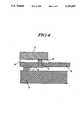
- FIG. 4is a cross section of an alternate embodiment of the chip carrier of FIG. 1 through section 2--2.
- an integrated circuit or semiconductor device 10contains an active surface 12 having interconnection pads 14 arranged in a configuration near the perimeter of the device.
- a circuit carrying substrate 16has an array of interconnection pads 18 that correspond to the interconnect pads 14 of the device.
- the substrate materialis typically a printed circuit board. Circuit boards made from materials with low expansion coefficients are preferred (between about 6 and about 18 in/in/°C ⁇ 10 -6 ).
- One example of a useful materialis Thermount E-215/CE laminate from the DuPont Corporation of Wilmington, Del. This laminate is an epoxy resin reinforced with aramid fiber. Other types of organic resin such as polyesters, polyamides, polyimides, and modifications or blends of these resins may also be employed in conjunction with the aramid reinforcements.
- the substrate 16also contains other circuitry 20 that interconnects the pads to conductive thru-holes or vias 22 in the substrate.
- the circuitry 20may also be connected to semicircular conductive thru-holes 24 on the perimeter of the substrate.
- each of the integrated circuit interconnect pads 14may be routed to a corresponding solder pad on the bottom of the substrate 16.
- the lines and spaces required for the solder padsare much larger than those on the integrated circuit device since he entire surface of the substrate may be used.
- spaces between interconnect pads on an integrated circuit deviceare typically 0.004 inches.
- the spacings between the solder pads on the bottom of the substratemay be as great as 0.030 inches.
- the solder pad diametersmay be as great as 0.030 inches as opposed to 0.004 inches on the device interconnect pads.
- the semiconductor device 10is attached to the substrate by facing the active surface 12 of the device 10 toward the upper surface of the substrate 16. Interconnection of the device to the substrate is provided by means of conducive bumps 26 between the pads 14 of the device and the circuitry 18 of the substrate. These bumps may typically be made from solder or be thermocompression bonds, conductive epoxy, or conductive elastomer. If they are made from solder, the device is attached to the substrate by means of the control-collapse-chip-connection (C4). This type of connection is well known to those skilled in the art and has been utilized to achieve high-density circuitry.
- C4control-collapse-chip-connection
- the chip carrierin accordance with the present invention once completed, does not require a clean room environment in order to be attached to a main circuit board.
- the COB processrequires cleanroom conditions for assembly to the main circuit board.
- an organic coupling agent 28may be applied in the gap between the integrated circuit and the substrate.
- This coupling agentmay be, for example, a rigid adhesive such as an epoxy or a softer material such as a silicone.
- An example of a suitable coupling agentis Hysol FP 4510, an epoxy from the Dexter Corporation of Industry, California.
- the coupling agentserves to provide additional mechanical bonding between the device and the substrate and also serves as a stress relieving member.
- the third function of the coupling agentis to environmentally protect the active surface of the device and the interconnections. Depending on the application, the coupling agent may cover the entire gap between the device and the substrate or may only cover a portion of the active surface of the device.
- the integrated circuit 10lies over some of the conductive thru-holes 22.
- Each of the conductive thru-holes 22connects to a solder pad 23 on the bottom side of the substrate 16.
- the organic coupling agent or underfill material 28fills the gap between the device 10 and the substrate 16.
- the interconnect pads 14 of the device 10are connected to the circuitry pads 18 of the substrate by means of a metallic bump 26.
- the overall size of the substrate 16is only slightly larger than the overall size of the integrated circuit 10.
- the length and width of the substrateis no greater than 0.15 inches greater than the length and width of the device and may be as small as the device itself in some cases.
- the substrateis 0.025 to 0.1 inches greater than the largest dimension of the device.
- the assembled integrated circuit chip carriermay now be electrically tested with conventional testing equipment, without having to resort to expensive and complex semiconductor testing equipment. Since the carrier is tested at a package level, the testing regime can be more thorough, and does not require the complexity and minaturization necessary for testing at the wafer level.
- the assemblymay now be placed onto a printed circuit board 25 by any number of interconnection schemes.
- the integrated circuit assemblymay be attached to the circuit board by solder joints as in the C5 process (controlled collapse chip carrier connection) or it may be attached using elastomeric interconnects of hot-melt adhesive interconnects.
- solder joints 27are achieved by reflowing solder balls between the assembly and the circuit board.
- an alternate embodiment of the inventioncomprises attaching the semiconductor device 10 to a substrate 36 containing circuitry patterns 18 on one side only.
- the device 10is directly attached via solder bumps 26 to the circuitry pattern on the top side of the substrate 36 to create a chip carrier assembly.
- the circuitry patternextends to a hole 22 in the substrate, and may terminate in an annular ring around the hole or may cover the hole entirely so as to tent the hole.
- the assemblymay contain the above referenced organic coupling agent 28 is desired.
- the carrieris soldered to the PCB using additional, usually larger, solder bumps 37.
- the solder bumps 37are soldered to the circuitry pattern 18 by forming the bumps in the substrate hole 32 so that the solder 37 connects to the back side of the circuitry pattern 18.
- a semiconductor device 10is attached to a substrate 46 having a circuitry pattern 48 on the back side of the substrate.
- the deviceis connected to the back side of the circuitry pattern via a series of solder bumps 46 that extend through a hole 42 in the substrate to create a chip carrier assembly.
- the assemblymay contain the above referenced organic coupling agent 28 if desired.
- the carrieris soldered to the PCB using additional, usually larger, solder bumps 47.
- the solder bumps 47are soldered to the circuitry pattern 48 and the PCB 25 using, for example, a C5 process.
- a package created in accordance with the inventionprovides numerous advantages, amongst which are: a package with a smaller footprint than conventional chip carrier packages, a package with a footprint only slightly larger than the actual size of the integrated circuit itself, a package with significantly reduced height (only slightly greater than the height of the integrated circuit), a package that may be easily tested prior to assembly to a main circuit board, and a package that does not require clean room environments for assembling an integrated circuit to a main circuit board.
- the present inventionsatisfies a long-existing need for an improved integrated circuit chip carrier that is smaller in size, more reliable, lower cost, easier to manufacture, and is electrically testable.
Landscapes
- Engineering & Computer Science (AREA)
- Physics & Mathematics (AREA)
- Condensed Matter Physics & Semiconductors (AREA)
- General Physics & Mathematics (AREA)
- Computer Hardware Design (AREA)
- Microelectronics & Electronic Packaging (AREA)
- Power Engineering (AREA)
- Manufacturing & Machinery (AREA)
- Wire Bonding (AREA)
Abstract
Description
Claims (14)
Priority Applications (1)
| Application Number | Priority Date | Filing Date | Title |
|---|---|---|---|
| US07/898,231US5293067A (en) | 1991-05-23 | 1992-06-12 | Integrated circuit chip carrier |
Applications Claiming Priority (2)
| Application Number | Priority Date | Filing Date | Title |
|---|---|---|---|
| US70447191A | 1991-05-23 | 1991-05-23 | |
| US07/898,231US5293067A (en) | 1991-05-23 | 1992-06-12 | Integrated circuit chip carrier |
Related Parent Applications (1)
| Application Number | Title | Priority Date | Filing Date |
|---|---|---|---|
| US70447191AContinuation | 1991-05-23 | 1991-05-23 |
Publications (1)
| Publication Number | Publication Date |
|---|---|
| US5293067Atrue US5293067A (en) | 1994-03-08 |
Family
ID=24829653
Family Applications (1)
| Application Number | Title | Priority Date | Filing Date |
|---|---|---|---|
| US07/898,231Expired - LifetimeUS5293067A (en) | 1991-05-23 | 1992-06-12 | Integrated circuit chip carrier |
Country Status (5)
| Country | Link |
|---|---|
| US (1) | US5293067A (en) |
| EP (1) | EP0585376A4 (en) |
| JP (1) | JP2570498B2 (en) |
| KR (1) | KR970011620B1 (en) |
| WO (1) | WO1992021150A1 (en) |
Cited By (94)
| Publication number | Priority date | Publication date | Assignee | Title |
|---|---|---|---|---|
| US5418471A (en)* | 1994-01-26 | 1995-05-23 | Emulation Technology, Inc. | Adapter which emulates ball grid array packages |
| US5427984A (en)* | 1993-03-01 | 1995-06-27 | At&T Global Information Solutions | Method of making a cooling package for a semiconductor chip |
| US5444303A (en)* | 1994-08-10 | 1995-08-22 | Motorola, Inc. | Wire bond pad arrangement having improved pad density |
| US5501006A (en)* | 1993-09-22 | 1996-03-26 | Motorola, Inc. | Method for connection of signals to an integrated circuit |
| US5625224A (en)* | 1994-08-10 | 1997-04-29 | Motorola, Inc. | Method and apparatus for an integrated circuit chip carrier having improved mounting pad density |
| US5637916A (en)* | 1996-02-02 | 1997-06-10 | National Semiconductor Corporation | Carrier based IC packaging arrangement |
| US5731709A (en)* | 1996-01-26 | 1998-03-24 | Motorola, Inc. | Method for testing a ball grid array semiconductor device and a device for such testing |
| US5814401A (en)* | 1997-02-04 | 1998-09-29 | Motorola, Inc. | Selectively filled adhesive film containing a fluxing agent |
| US5821597A (en)* | 1992-09-11 | 1998-10-13 | Semiconductor Energy Laboratory Co., Ltd. | Photoelectric conversion device |
| US5847456A (en)* | 1996-02-28 | 1998-12-08 | Nec Corporation | Semiconductor device |
| USRE36442E (en)* | 1994-01-26 | 1999-12-14 | Emulation Technology, Inc. | Adapter which emulates ball grid array packages |
| US6007348A (en)* | 1996-05-07 | 1999-12-28 | Advanced Intercommunications Corporation | Solder ball terminal |
| US6013944A (en)* | 1997-02-10 | 2000-01-11 | Fujitsu Limited | Semiconductor device in which chip electrodes are connected to terminals arranged along the periphery of an insulative board |
| US6093971A (en)* | 1996-10-14 | 2000-07-25 | Fraunhofer-Gesellschaft Zur Forderung Der Angewandten Forschung E.V. | Chip module with conductor paths on the chip bonding side of a chip carrier |
| US6144090A (en)* | 1997-02-13 | 2000-11-07 | Fujitsu Limited | Ball grid array package having electrodes on peripheral side surfaces of a package board |
| US6147876A (en)* | 1993-09-14 | 2000-11-14 | Kabushiki Kaisha Toshiba | Multi-chip module having printed wiring board comprising circuit pattern for IC chip |
| US6163076A (en)* | 1999-06-04 | 2000-12-19 | Advanced Semiconductor Engineering, Inc. | Stacked structure of semiconductor package |
| US6278178B1 (en)* | 1998-02-10 | 2001-08-21 | Hyundai Electronics Industries Co., Ltd. | Integrated device package and fabrication methods thereof |
| US6281571B1 (en)* | 1999-03-26 | 2001-08-28 | Fujitsu Limited | Semiconductor device having an external connection electrode extending through a through hole formed in a substrate |
| US6287893B1 (en) | 1997-10-20 | 2001-09-11 | Flip Chip Technologies, L.L.C. | Method for forming chip scale package |
| US6291776B1 (en)* | 1998-11-03 | 2001-09-18 | International Business Machines Corporation | Thermal deformation management for chip carriers |
| US6308938B1 (en) | 1997-09-26 | 2001-10-30 | Mitsubishi Denki Kabushiki Kaisha | Semiconductor integrated circuit device |
| US6316830B1 (en) | 1998-12-17 | 2001-11-13 | Charles Wen Chyang Lin | Bumpless flip chip assembly with strips and via-fill |
| US6350632B1 (en) | 2000-09-20 | 2002-02-26 | Charles W. C. Lin | Semiconductor chip assembly with ball bond connection joint |
| US6350633B1 (en) | 2000-08-22 | 2002-02-26 | Charles W. C. Lin | Semiconductor chip assembly with simultaneously electroplated contact terminal and connection joint |
| US6350386B1 (en)* | 2000-09-20 | 2002-02-26 | Charles W. C. Lin | Method of making a support circuit with a tapered through-hole for a semiconductor chip assembly |
| US20020030272A1 (en)* | 1998-02-17 | 2002-03-14 | Akihiro Murata | Semiconductor apparatus substrate, semiconductor apparatus, and method of manufacturing thereof and electronic apparatus |
| US6403460B1 (en) | 2000-08-22 | 2002-06-11 | Charles W. C. Lin | Method of making a semiconductor chip assembly |
| US6403400B2 (en) | 1998-12-17 | 2002-06-11 | Charles Wen Chyang Lin | Bumpless flip chip assembly with strips-in-via and plating |
| US6402970B1 (en) | 2000-08-22 | 2002-06-11 | Charles W. C. Lin | Method of making a support circuit for a semiconductor chip assembly |
| US6406939B1 (en) | 1998-05-02 | 2002-06-18 | Charles W. C. Lin | Flip chip assembly with via interconnection |
| US20020093803A1 (en)* | 2001-01-17 | 2002-07-18 | Honeywell International, Inc. | Adapter for plastic-leaded chip carrier (PLCC) and other surface mount technology (SMT) chip carriers |
| US6436734B1 (en) | 2000-08-22 | 2002-08-20 | Charles W. C. Lin | Method of making a support circuit for a semiconductor chip assembly |
| US6440835B1 (en) | 2000-10-13 | 2002-08-27 | Charles W. C. Lin | Method of connecting a conductive trace to a semiconductor chip |
| US6444489B1 (en) | 2000-12-15 | 2002-09-03 | Charles W. C. Lin | Semiconductor chip assembly with bumped molded substrate |
| US6448644B1 (en) | 1998-05-02 | 2002-09-10 | Charles W. C. Lin | Flip chip assembly with via interconnection |
| US6448108B1 (en) | 2000-10-02 | 2002-09-10 | Charles W. C. Lin | Method of making a semiconductor chip assembly with a conductive trace subtractively formed before and after chip attachment |
| US20020155728A1 (en)* | 1990-09-24 | 2002-10-24 | Tessera, Inc. | Semiconductor chip assemblies, methods of making same and components for same |
| US6492252B1 (en) | 2000-10-13 | 2002-12-10 | Bridge Semiconductor Corporation | Method of connecting a bumped conductive trace to a semiconductor chip |
| US6511865B1 (en) | 2000-09-20 | 2003-01-28 | Charles W. C. Lin | Method for forming a ball bond connection joint on a conductive trace and conductive pad in a semiconductor chip assembly |
| US6528891B2 (en) | 1998-12-17 | 2003-03-04 | Charles Wen Chyang Lin | Bumpless flip chip assembly with solder via |
| US6537851B1 (en) | 2000-10-13 | 2003-03-25 | Bridge Semiconductor Corporation | Method of connecting a bumped compliant conductive trace to a semiconductor chip |
| US20030057974A1 (en)* | 2001-09-26 | 2003-03-27 | Mccormick Carolyn | Arrangement of vias in a substrate to support a ball grid array |
| US6544813B1 (en) | 2000-10-02 | 2003-04-08 | Charles W. C. Lin | Method of making a semiconductor chip assembly with a conductive trace subtractively formed before and after chip attachment |
| US6548393B1 (en) | 2000-10-13 | 2003-04-15 | Charles W. C. Lin | Semiconductor chip assembly with hardened connection joint |
| US6551861B1 (en) | 2000-08-22 | 2003-04-22 | Charles W. C. Lin | Method of making a semiconductor chip assembly by joining the chip to a support circuit with an adhesive |
| US6562657B1 (en) | 2000-08-22 | 2003-05-13 | Charles W. C. Lin | Semiconductor chip assembly with simultaneously electrolessly plated contact terminal and connection joint |
| US6562709B1 (en) | 2000-08-22 | 2003-05-13 | Charles W. C. Lin | Semiconductor chip assembly with simultaneously electroplated contact terminal and connection joint |
| US6576493B1 (en) | 2000-10-13 | 2003-06-10 | Bridge Semiconductor Corporation | Method of connecting a conductive trace and an insulative base to a semiconductor chip using multiple etch steps |
| US6576539B1 (en) | 2000-10-13 | 2003-06-10 | Charles W.C. Lin | Semiconductor chip assembly with interlocked conductive trace |
| US6583040B1 (en) | 2000-10-13 | 2003-06-24 | Bridge Semiconductor Corporation | Method of making a pillar in a laminated structure for a semiconductor chip assembly |
| US6653170B1 (en) | 2001-02-06 | 2003-11-25 | Charles W. C. Lin | Semiconductor chip assembly with elongated wire ball bonded to chip and electrolessly plated to support circuit |
| US6660626B1 (en) | 2000-08-22 | 2003-12-09 | Charles W. C. Lin | Semiconductor chip assembly with simultaneously electrolessly plated contact terminal and connection joint |
| US6667229B1 (en) | 2000-10-13 | 2003-12-23 | Bridge Semiconductor Corporation | Method of connecting a bumped compliant conductive trace and an insulative base to a semiconductor chip |
| DE10227059A1 (en)* | 2002-06-17 | 2004-01-15 | Infineon Technologies Ag | Packaging for semiconductor devices and method of manufacturing the same |
| US6699780B1 (en) | 2000-10-13 | 2004-03-02 | Bridge Semiconductor Corporation | Method of connecting a conductive trace to a semiconductor chip using plasma undercut etching |
| US6720576B1 (en) | 1992-09-11 | 2004-04-13 | Semiconductor Energy Laboratory Co., Ltd. | Plasma processing method and photoelectric conversion device |
| US6740576B1 (en) | 2000-10-13 | 2004-05-25 | Bridge Semiconductor Corporation | Method of making a contact terminal with a plated metal peripheral sidewall portion for a semiconductor chip assembly |
| US20040105244A1 (en)* | 2002-08-06 | 2004-06-03 | Ilyas Mohammed | Lead assemblies with offset portions and microelectronic assemblies with leads having offset portions |
| DE10323296A1 (en)* | 2003-05-21 | 2005-01-05 | Infineon Technologies Ag | Arrangement for stress reduction for substrate-based chip packages has uniform trench-shaped structures on chip side of substrate to interrupt or displace thermally induced mechanical stress |
| US6872591B1 (en) | 2000-10-13 | 2005-03-29 | Bridge Semiconductor Corporation | Method of making a semiconductor chip assembly with a conductive trace and a substrate |
| US6876072B1 (en) | 2000-10-13 | 2005-04-05 | Bridge Semiconductor Corporation | Semiconductor chip assembly with chip in substrate cavity |
| US6908788B1 (en) | 2000-10-13 | 2005-06-21 | Bridge Semiconductor Corporation | Method of connecting a conductive trace to a semiconductor chip using a metal base |
| US6949408B1 (en) | 2000-10-13 | 2005-09-27 | Bridge Semiconductor Corporation | Method of connecting a conductive trace and an insulative base to a semiconductor chip using multiple etch steps |
| US6984576B1 (en) | 2000-10-13 | 2006-01-10 | Bridge Semiconductor Corporation | Method of connecting an additively and subtractively formed conductive trace and an insulative base to a semiconductor chip |
| US20060012024A1 (en)* | 2000-10-13 | 2006-01-19 | Bridge Semiconductor Corporation | Semiconductor chip assembly with metal containment wall and solder terminal |
| US7009297B1 (en) | 2000-10-13 | 2006-03-07 | Bridge Semiconductor Corporation | Semiconductor chip assembly with embedded metal particle |
| US7071089B1 (en) | 2000-10-13 | 2006-07-04 | Bridge Semiconductor Corporation | Method of making a semiconductor chip assembly with a carved bumped terminal |
| US7075186B1 (en) | 2000-10-13 | 2006-07-11 | Bridge Semiconductor Corporation | Semiconductor chip assembly with interlocked contact terminal |
| US7094676B1 (en) | 2000-10-13 | 2006-08-22 | Bridge Semiconductor Corporation | Semiconductor chip assembly with embedded metal pillar |
| US7112521B1 (en) | 2000-10-13 | 2006-09-26 | Bridge Semiconductor Corporation | Method of making a semiconductor chip assembly with a bumped metal pillar |
| US7129113B1 (en) | 2000-10-13 | 2006-10-31 | Bridge Semiconductor Corporation | Method of making a three-dimensional stacked semiconductor package with a metal pillar in an encapsulant aperture |
| US7132741B1 (en) | 2000-10-13 | 2006-11-07 | Bridge Semiconductor Corporation | Semiconductor chip assembly with carved bumped terminal |
| US7190080B1 (en) | 2000-10-13 | 2007-03-13 | Bridge Semiconductor Corporation | Semiconductor chip assembly with embedded metal pillar |
| US7229857B2 (en) | 2002-01-14 | 2007-06-12 | Infineon Technologies Ag | Method for producing a protection for chip edges and system for the protection of chip edges |
| US7262082B1 (en) | 2000-10-13 | 2007-08-28 | Bridge Semiconductor Corporation | Method of making a three-dimensional stacked semiconductor package with a metal pillar and a conductive interconnect in an encapsulant aperture |
| US7264991B1 (en) | 2000-10-13 | 2007-09-04 | Bridge Semiconductor Corporation | Method of connecting a conductive trace to a semiconductor chip using conductive adhesive |
| US7268421B1 (en) | 2004-11-10 | 2007-09-11 | Bridge Semiconductor Corporation | Semiconductor chip assembly with welded metal pillar that includes enlarged ball bond |
| US7319265B1 (en) | 2000-10-13 | 2008-01-15 | Bridge Semiconductor Corporation | Semiconductor chip assembly with precision-formed metal pillar |
| US7396703B1 (en) | 2003-11-20 | 2008-07-08 | Bridge Semiconductor Corporation | Method of making a semiconductor chip assembly with a bumped terminal and a filler |
| US7446419B1 (en) | 2004-11-10 | 2008-11-04 | Bridge Semiconductor Corporation | Semiconductor chip assembly with welded metal pillar of stacked metal balls |
| US7476110B2 (en) | 1996-10-10 | 2009-01-13 | Fci Americas Technology, Inc. | High density connector and method of manufacture |
| US7494843B1 (en) | 2006-12-26 | 2009-02-24 | Bridge Semiconductor Corporation | Method of making a semiconductor chip assembly with thermal conductor and encapsulant grinding |
| US7538415B1 (en) | 2003-11-20 | 2009-05-26 | Bridge Semiconductor Corporation | Semiconductor chip assembly with bumped terminal, filler and insulative base |
| US7750483B1 (en) | 2004-11-10 | 2010-07-06 | Bridge Semiconductor Corporation | Semiconductor chip assembly with welded metal pillar and enlarged plated contact terminal |
| US7811863B1 (en) | 2006-10-26 | 2010-10-12 | Bridge Semiconductor Corporation | Method of making a semiconductor chip assembly with metal pillar and encapsulant grinding and heat sink attachment |
| US20110019379A1 (en)* | 2009-07-22 | 2011-01-27 | Nec Electronics Corporation | Printed wiring board, semiconductor device, and method for manufacturing printed wiring board |
| US7993983B1 (en) | 2003-11-17 | 2011-08-09 | Bridge Semiconductor Corporation | Method of making a semiconductor chip assembly with chip and encapsulant grinding |
| USD668658S1 (en)* | 2011-11-15 | 2012-10-09 | Connectblue Ab | Module |
| USD668659S1 (en)* | 2011-11-15 | 2012-10-09 | Connectblue Ab | Module |
| USD680119S1 (en)* | 2011-11-15 | 2013-04-16 | Connectblue Ab | Module |
| USD680545S1 (en)* | 2011-11-15 | 2013-04-23 | Connectblue Ab | Module |
| USD689053S1 (en)* | 2011-11-15 | 2013-09-03 | Connectblue Ab | Module |
| USD692896S1 (en)* | 2011-11-15 | 2013-11-05 | Connectblue Ab | Module |
Families Citing this family (9)
| Publication number | Priority date | Publication date | Assignee | Title |
|---|---|---|---|---|
| US5611140A (en)* | 1989-12-18 | 1997-03-18 | Epoxy Technology, Inc. | Method of forming electrically conductive polymer interconnects on electrical substrates |
| JP3247384B2 (en) | 1994-03-18 | 2002-01-15 | 日立化成工業株式会社 | Semiconductor package manufacturing method and semiconductor package |
| US5677246A (en)* | 1994-11-29 | 1997-10-14 | Kabushiki Kaisha Toshiba | Method of manufacturing semiconductor devices |
| JPH08236654A (en) | 1995-02-23 | 1996-09-13 | Matsushita Electric Ind Co Ltd | Chip carrier and manufacturing method thereof |
| JP3726318B2 (en)* | 1995-08-22 | 2005-12-14 | 株式会社日立製作所 | Chip size package, manufacturing method thereof, and second level packaging |
| JP3176307B2 (en)* | 1997-03-03 | 2001-06-18 | 日本電気株式会社 | Mounting structure of integrated circuit device and method of manufacturing the same |
| RU2134466C1 (en) | 1998-12-08 | 1999-08-10 | Таран Александр Иванович | Carrier of crystal of integrated circuit |
| JP2016178001A (en)* | 2015-03-20 | 2016-10-06 | カシオ計算機株式会社 | Connector and electronic apparatus |
| JP2016178068A (en)* | 2015-03-23 | 2016-10-06 | カシオ計算機株式会社 | Connector and electronic apparatus |
Citations (13)
| Publication number | Priority date | Publication date | Assignee | Title |
|---|---|---|---|---|
| JPS5994441A (en)* | 1982-11-19 | 1984-05-31 | Nippon Denso Co Ltd | Semiconductor device |
| JPS60154632A (en)* | 1984-01-25 | 1985-08-14 | Hitachi Ltd | Semiconductor device |
| JPS6127667A (en)* | 1984-07-17 | 1986-02-07 | Mitsubishi Electric Corp | Semiconductor device |
| JPS61279164A (en)* | 1985-06-05 | 1986-12-09 | Hitachi Ltd | Multichip module |
| JPS6252930A (en)* | 1985-09-02 | 1987-03-07 | Canon Inc | Semiconductor manufacture equipment |
| JPS63301552A (en)* | 1987-06-01 | 1988-12-08 | Nec Corp | Wiring substrate |
| US4821142A (en)* | 1986-06-06 | 1989-04-11 | Hitachi, Ltd. | Ceramic multilayer circuit board and semiconductor module |
| JPH01132150A (en)* | 1987-11-18 | 1989-05-24 | Hitachi Ltd | Semiconductor chip carrier substrate |
| JPH023263A (en)* | 1988-06-20 | 1990-01-08 | Nec Corp | Semiconductor device |
| US4893172A (en)* | 1987-01-19 | 1990-01-09 | Hitachi, Ltd. | Connecting structure for electronic part and method of manufacturing the same |
| US4933810A (en)* | 1987-04-30 | 1990-06-12 | Honeywell Inc. | Integrated circuit interconnector |
| US4954878A (en)* | 1989-06-29 | 1990-09-04 | Digital Equipment Corp. | Method of packaging and powering integrated circuit chips and the chip assembly formed thereby |
| US4963414A (en)* | 1989-06-12 | 1990-10-16 | General Electric Company | Low thermal expansion, heat sinking substrate for electronic surface mount applications |
Family Cites Families (3)
| Publication number | Priority date | Publication date | Assignee | Title |
|---|---|---|---|---|
| JPS599441A (en)* | 1982-07-08 | 1984-01-18 | Yamatake Honeywell Co Ltd | Starting operation of heat source equipment |
| EP0351581A1 (en)* | 1988-07-22 | 1990-01-24 | Oerlikon-Contraves AG | High-density integrated circuit and method for its production |
| JPH0269945A (en)* | 1988-09-05 | 1990-03-08 | Hitachi Ltd | Semiconductor device and its manufacturing method |
- 1992
- 1992-04-23JPJP5500049Apatent/JP2570498B2/ennot_activeExpired - Lifetime
- 1992-04-23EPEP19920912829patent/EP0585376A4/ennot_activeWithdrawn
- 1992-04-23KRKR1019930702937Apatent/KR970011620B1/ennot_activeExpired - Lifetime
- 1992-04-23WOPCT/US1992/003361patent/WO1992021150A1/ennot_activeApplication Discontinuation
- 1992-06-12USUS07/898,231patent/US5293067A/ennot_activeExpired - Lifetime
Patent Citations (13)
| Publication number | Priority date | Publication date | Assignee | Title |
|---|---|---|---|---|
| JPS5994441A (en)* | 1982-11-19 | 1984-05-31 | Nippon Denso Co Ltd | Semiconductor device |
| JPS60154632A (en)* | 1984-01-25 | 1985-08-14 | Hitachi Ltd | Semiconductor device |
| JPS6127667A (en)* | 1984-07-17 | 1986-02-07 | Mitsubishi Electric Corp | Semiconductor device |
| JPS61279164A (en)* | 1985-06-05 | 1986-12-09 | Hitachi Ltd | Multichip module |
| JPS6252930A (en)* | 1985-09-02 | 1987-03-07 | Canon Inc | Semiconductor manufacture equipment |
| US4821142A (en)* | 1986-06-06 | 1989-04-11 | Hitachi, Ltd. | Ceramic multilayer circuit board and semiconductor module |
| US4893172A (en)* | 1987-01-19 | 1990-01-09 | Hitachi, Ltd. | Connecting structure for electronic part and method of manufacturing the same |
| US4933810A (en)* | 1987-04-30 | 1990-06-12 | Honeywell Inc. | Integrated circuit interconnector |
| JPS63301552A (en)* | 1987-06-01 | 1988-12-08 | Nec Corp | Wiring substrate |
| JPH01132150A (en)* | 1987-11-18 | 1989-05-24 | Hitachi Ltd | Semiconductor chip carrier substrate |
| JPH023263A (en)* | 1988-06-20 | 1990-01-08 | Nec Corp | Semiconductor device |
| US4963414A (en)* | 1989-06-12 | 1990-10-16 | General Electric Company | Low thermal expansion, heat sinking substrate for electronic surface mount applications |
| US4954878A (en)* | 1989-06-29 | 1990-09-04 | Digital Equipment Corp. | Method of packaging and powering integrated circuit chips and the chip assembly formed thereby |
Cited By (142)
| Publication number | Priority date | Publication date | Assignee | Title |
|---|---|---|---|---|
| US7271481B2 (en) | 1990-09-24 | 2007-09-18 | Tessera, Inc. | Microelectronic component and assembly having leads with offset portions |
| US20050087855A1 (en)* | 1990-09-24 | 2005-04-28 | Tessera, Inc. | Microelectronic component and assembly having leads with offset portions |
| US7098078B2 (en) | 1990-09-24 | 2006-08-29 | Tessera, Inc. | Microelectronic component and assembly having leads with offset portions |
| US20030168253A1 (en)* | 1990-09-24 | 2003-09-11 | Tessera, Inc. | Microelectronic component and assembly having leads with offset portions |
| US20020155728A1 (en)* | 1990-09-24 | 2002-10-24 | Tessera, Inc. | Semiconductor chip assemblies, methods of making same and components for same |
| US7095090B2 (en) | 1992-09-11 | 2006-08-22 | Semiconductor Energy Laboratory Co., Ltd. | Photoelectric conversion device |
| US5821597A (en)* | 1992-09-11 | 1998-10-13 | Semiconductor Energy Laboratory Co., Ltd. | Photoelectric conversion device |
| US20040188680A1 (en)* | 1992-09-11 | 2004-09-30 | Semiconductor Energy Laboratory Co., Ltd. | Plasma processing method and photoelectric conversion device |
| US6720576B1 (en) | 1992-09-11 | 2004-04-13 | Semiconductor Energy Laboratory Co., Ltd. | Plasma processing method and photoelectric conversion device |
| US5427984A (en)* | 1993-03-01 | 1995-06-27 | At&T Global Information Solutions | Method of making a cooling package for a semiconductor chip |
| US6418030B1 (en) | 1993-09-14 | 2002-07-09 | Kabushiki Kaisha Toshiba | Multi-chip module |
| US6147876A (en)* | 1993-09-14 | 2000-11-14 | Kabushiki Kaisha Toshiba | Multi-chip module having printed wiring board comprising circuit pattern for IC chip |
| US5501006A (en)* | 1993-09-22 | 1996-03-26 | Motorola, Inc. | Method for connection of signals to an integrated circuit |
| USRE36442E (en)* | 1994-01-26 | 1999-12-14 | Emulation Technology, Inc. | Adapter which emulates ball grid array packages |
| US5418471A (en)* | 1994-01-26 | 1995-05-23 | Emulation Technology, Inc. | Adapter which emulates ball grid array packages |
| US5625224A (en)* | 1994-08-10 | 1997-04-29 | Motorola, Inc. | Method and apparatus for an integrated circuit chip carrier having improved mounting pad density |
| US5444303A (en)* | 1994-08-10 | 1995-08-22 | Motorola, Inc. | Wire bond pad arrangement having improved pad density |
| US5731709A (en)* | 1996-01-26 | 1998-03-24 | Motorola, Inc. | Method for testing a ball grid array semiconductor device and a device for such testing |
| US5765280A (en)* | 1996-02-02 | 1998-06-16 | National Semiconductor Corporation | Method for making a carrier based IC packaging arrangement |
| US5637916A (en)* | 1996-02-02 | 1997-06-10 | National Semiconductor Corporation | Carrier based IC packaging arrangement |
| US5847456A (en)* | 1996-02-28 | 1998-12-08 | Nec Corporation | Semiconductor device |
| US6007348A (en)* | 1996-05-07 | 1999-12-28 | Advanced Intercommunications Corporation | Solder ball terminal |
| US6325280B1 (en) | 1996-05-07 | 2001-12-04 | Advanced Interconnections Corporation | Solder ball terminal |
| US7476110B2 (en) | 1996-10-10 | 2009-01-13 | Fci Americas Technology, Inc. | High density connector and method of manufacture |
| US8167630B2 (en) | 1996-10-10 | 2012-05-01 | Fci Americas Technology Llc | High density connector and method of manufacture |
| US6093971A (en)* | 1996-10-14 | 2000-07-25 | Fraunhofer-Gesellschaft Zur Forderung Der Angewandten Forschung E.V. | Chip module with conductor paths on the chip bonding side of a chip carrier |
| CN1097305C (en)* | 1997-02-04 | 2002-12-25 | 摩托罗拉公司 | Selectively filled adhesive film containing fluxing agent |
| US5814401A (en)* | 1997-02-04 | 1998-09-29 | Motorola, Inc. | Selectively filled adhesive film containing a fluxing agent |
| US6013944A (en)* | 1997-02-10 | 2000-01-11 | Fujitsu Limited | Semiconductor device in which chip electrodes are connected to terminals arranged along the periphery of an insulative board |
| US6144090A (en)* | 1997-02-13 | 2000-11-07 | Fujitsu Limited | Ball grid array package having electrodes on peripheral side surfaces of a package board |
| US6308938B1 (en) | 1997-09-26 | 2001-10-30 | Mitsubishi Denki Kabushiki Kaisha | Semiconductor integrated circuit device |
| US6750135B2 (en) | 1997-10-20 | 2004-06-15 | Flip Chip Technologies, L.L.C. | Method for forming chip scale package |
| US6441487B2 (en) | 1997-10-20 | 2002-08-27 | Flip Chip Technologies, L.L.C. | Chip scale package using large ductile solder balls |
| US6287893B1 (en) | 1997-10-20 | 2001-09-11 | Flip Chip Technologies, L.L.C. | Method for forming chip scale package |
| US6278178B1 (en)* | 1998-02-10 | 2001-08-21 | Hyundai Electronics Industries Co., Ltd. | Integrated device package and fabrication methods thereof |
| US6803251B2 (en) | 1998-02-10 | 2004-10-12 | Hyundai Electronics Industries Co., Ltd. | Integrated device package and fabrication methods thereof |
| US20020030272A1 (en)* | 1998-02-17 | 2002-03-14 | Akihiro Murata | Semiconductor apparatus substrate, semiconductor apparatus, and method of manufacturing thereof and electronic apparatus |
| US6406939B1 (en) | 1998-05-02 | 2002-06-18 | Charles W. C. Lin | Flip chip assembly with via interconnection |
| US6448644B1 (en) | 1998-05-02 | 2002-09-10 | Charles W. C. Lin | Flip chip assembly with via interconnection |
| US6291776B1 (en)* | 1998-11-03 | 2001-09-18 | International Business Machines Corporation | Thermal deformation management for chip carriers |
| KR100368630B1 (en)* | 1998-11-03 | 2003-01-24 | 인터내셔널 비지네스 머신즈 코포레이션 | Thermal deformation management for chip carriers |
| SG89300A1 (en)* | 1998-11-03 | 2002-06-18 | Ibm | Thermal deformation management for chip carriers |
| US6437452B2 (en) | 1998-12-17 | 2002-08-20 | Charles Wen Chyang Lin | Bumpless flip chip assembly with strips-in-via and plating |
| US6528891B2 (en) | 1998-12-17 | 2003-03-04 | Charles Wen Chyang Lin | Bumpless flip chip assembly with solder via |
| US6475833B2 (en) | 1998-12-17 | 2002-11-05 | Charles Wen Chyang Lin | Bumpless flip chip assembly with strips and via-fill |
| US6316830B1 (en) | 1998-12-17 | 2001-11-13 | Charles Wen Chyang Lin | Bumpless flip chip assembly with strips and via-fill |
| US6403400B2 (en) | 1998-12-17 | 2002-06-11 | Charles Wen Chyang Lin | Bumpless flip chip assembly with strips-in-via and plating |
| US6281571B1 (en)* | 1999-03-26 | 2001-08-28 | Fujitsu Limited | Semiconductor device having an external connection electrode extending through a through hole formed in a substrate |
| US6163076A (en)* | 1999-06-04 | 2000-12-19 | Advanced Semiconductor Engineering, Inc. | Stacked structure of semiconductor package |
| US6403460B1 (en) | 2000-08-22 | 2002-06-11 | Charles W. C. Lin | Method of making a semiconductor chip assembly |
| US6660626B1 (en) | 2000-08-22 | 2003-12-09 | Charles W. C. Lin | Semiconductor chip assembly with simultaneously electrolessly plated contact terminal and connection joint |
| US6436734B1 (en) | 2000-08-22 | 2002-08-20 | Charles W. C. Lin | Method of making a support circuit for a semiconductor chip assembly |
| US6402970B1 (en) | 2000-08-22 | 2002-06-11 | Charles W. C. Lin | Method of making a support circuit for a semiconductor chip assembly |
| US6350633B1 (en) | 2000-08-22 | 2002-02-26 | Charles W. C. Lin | Semiconductor chip assembly with simultaneously electroplated contact terminal and connection joint |
| US6551861B1 (en) | 2000-08-22 | 2003-04-22 | Charles W. C. Lin | Method of making a semiconductor chip assembly by joining the chip to a support circuit with an adhesive |
| US6562657B1 (en) | 2000-08-22 | 2003-05-13 | Charles W. C. Lin | Semiconductor chip assembly with simultaneously electrolessly plated contact terminal and connection joint |
| US6562709B1 (en) | 2000-08-22 | 2003-05-13 | Charles W. C. Lin | Semiconductor chip assembly with simultaneously electroplated contact terminal and connection joint |
| US6511865B1 (en) | 2000-09-20 | 2003-01-28 | Charles W. C. Lin | Method for forming a ball bond connection joint on a conductive trace and conductive pad in a semiconductor chip assembly |
| US6350632B1 (en) | 2000-09-20 | 2002-02-26 | Charles W. C. Lin | Semiconductor chip assembly with ball bond connection joint |
| US6350386B1 (en)* | 2000-09-20 | 2002-02-26 | Charles W. C. Lin | Method of making a support circuit with a tapered through-hole for a semiconductor chip assembly |
| US6627824B1 (en) | 2000-09-20 | 2003-09-30 | Charles W. C. Lin | Support circuit with a tapered through-hole for a semiconductor chip assembly |
| US6544813B1 (en) | 2000-10-02 | 2003-04-08 | Charles W. C. Lin | Method of making a semiconductor chip assembly with a conductive trace subtractively formed before and after chip attachment |
| US6448108B1 (en) | 2000-10-02 | 2002-09-10 | Charles W. C. Lin | Method of making a semiconductor chip assembly with a conductive trace subtractively formed before and after chip attachment |
| US6699780B1 (en) | 2000-10-13 | 2004-03-02 | Bridge Semiconductor Corporation | Method of connecting a conductive trace to a semiconductor chip using plasma undercut etching |
| US7129575B1 (en) | 2000-10-13 | 2006-10-31 | Bridge Semiconductor Corporation | Semiconductor chip assembly with bumped metal pillar |
| US6653217B1 (en) | 2000-10-13 | 2003-11-25 | Charles W. C. Lin | Method of connecting a conductive trace to a semiconductor chip |
| US6653742B1 (en) | 2000-10-13 | 2003-11-25 | Charles W. C. Lin | Semiconductor chip assembly with interlocked conductive trace |
| US6608374B1 (en) | 2000-10-13 | 2003-08-19 | Bridge Semiconductor Corporation | Semiconductor chip assembly with bumped conductive trace |
| US6667229B1 (en) | 2000-10-13 | 2003-12-23 | Bridge Semiconductor Corporation | Method of connecting a bumped compliant conductive trace and an insulative base to a semiconductor chip |
| US6673710B1 (en) | 2000-10-13 | 2004-01-06 | Bridge Semiconductor Corporation | Method of connecting a conductive trace and an insulative base to a semiconductor chip |
| US6440835B1 (en) | 2000-10-13 | 2002-08-27 | Charles W. C. Lin | Method of connecting a conductive trace to a semiconductor chip |
| US7419851B2 (en) | 2000-10-13 | 2008-09-02 | Bridge Semiconductor Corporation | Method of making a semiconductor chip assembly with a metal containment wall and a solder terminal |
| US6583040B1 (en) | 2000-10-13 | 2003-06-24 | Bridge Semiconductor Corporation | Method of making a pillar in a laminated structure for a semiconductor chip assembly |
| US6740576B1 (en) | 2000-10-13 | 2004-05-25 | Bridge Semiconductor Corporation | Method of making a contact terminal with a plated metal peripheral sidewall portion for a semiconductor chip assembly |
| US7414319B2 (en) | 2000-10-13 | 2008-08-19 | Bridge Semiconductor Corporation | Semiconductor chip assembly with metal containment wall and solder terminal |
| US6576539B1 (en) | 2000-10-13 | 2003-06-10 | Charles W.C. Lin | Semiconductor chip assembly with interlocked conductive trace |
| US6576493B1 (en) | 2000-10-13 | 2003-06-10 | Bridge Semiconductor Corporation | Method of connecting a conductive trace and an insulative base to a semiconductor chip using multiple etch steps |
| US6800506B1 (en) | 2000-10-13 | 2004-10-05 | Bridge Semiconductor Corporation | Method of making a bumped terminal in a laminated structure for a semiconductor chip assembly |
| US6548393B1 (en) | 2000-10-13 | 2003-04-15 | Charles W. C. Lin | Semiconductor chip assembly with hardened connection joint |
| US6809414B1 (en) | 2000-10-13 | 2004-10-26 | Bridge Semiconductor Corporation | Semiconductor chip assembly with bumped conductive trace |
| US7319265B1 (en) | 2000-10-13 | 2008-01-15 | Bridge Semiconductor Corporation | Semiconductor chip assembly with precision-formed metal pillar |
| US7264991B1 (en) | 2000-10-13 | 2007-09-04 | Bridge Semiconductor Corporation | Method of connecting a conductive trace to a semiconductor chip using conductive adhesive |
| US7262082B1 (en) | 2000-10-13 | 2007-08-28 | Bridge Semiconductor Corporation | Method of making a three-dimensional stacked semiconductor package with a metal pillar and a conductive interconnect in an encapsulant aperture |
| US6872591B1 (en) | 2000-10-13 | 2005-03-29 | Bridge Semiconductor Corporation | Method of making a semiconductor chip assembly with a conductive trace and a substrate |
| US6876072B1 (en) | 2000-10-13 | 2005-04-05 | Bridge Semiconductor Corporation | Semiconductor chip assembly with chip in substrate cavity |
| US7232707B1 (en) | 2000-10-13 | 2007-06-19 | Bridge Semiconductor Corporation | Method of making a semiconductor chip assembly with an interlocked contact terminal |
| US6908788B1 (en) | 2000-10-13 | 2005-06-21 | Bridge Semiconductor Corporation | Method of connecting a conductive trace to a semiconductor chip using a metal base |
| US6949408B1 (en) | 2000-10-13 | 2005-09-27 | Bridge Semiconductor Corporation | Method of connecting a conductive trace and an insulative base to a semiconductor chip using multiple etch steps |
| US6984576B1 (en) | 2000-10-13 | 2006-01-10 | Bridge Semiconductor Corporation | Method of connecting an additively and subtractively formed conductive trace and an insulative base to a semiconductor chip |
| US20060012024A1 (en)* | 2000-10-13 | 2006-01-19 | Bridge Semiconductor Corporation | Semiconductor chip assembly with metal containment wall and solder terminal |
| US20060014316A1 (en)* | 2000-10-13 | 2006-01-19 | Bridge Semiconductor Corporation | Method of making a semiconductor chip assemby with a metal containment wall and a solder terminal |
| US7009297B1 (en) | 2000-10-13 | 2006-03-07 | Bridge Semiconductor Corporation | Semiconductor chip assembly with embedded metal particle |
| US7015128B1 (en) | 2000-10-13 | 2006-03-21 | Bridge Semiconductor Corporation | Method of making a semiconductor chip assembly with an embedded metal particle |
| US7232706B1 (en) | 2000-10-13 | 2007-06-19 | Bridge Semiconductor Corporation | Method of making a semiconductor chip assembly with a precision-formed metal pillar |
| US7067911B1 (en) | 2000-10-13 | 2006-06-27 | Bridge Semiconductor Corporation | Three-dimensional stacked semiconductor package with metal pillar in encapsulant aperture |
| US7071573B1 (en) | 2000-10-13 | 2006-07-04 | Bridge Semiconductor Corporation | Semiconductor chip assembly with welded metal pillar |
| US7071089B1 (en) | 2000-10-13 | 2006-07-04 | Bridge Semiconductor Corporation | Method of making a semiconductor chip assembly with a carved bumped terminal |
| US7075186B1 (en) | 2000-10-13 | 2006-07-11 | Bridge Semiconductor Corporation | Semiconductor chip assembly with interlocked contact terminal |
| US7094676B1 (en) | 2000-10-13 | 2006-08-22 | Bridge Semiconductor Corporation | Semiconductor chip assembly with embedded metal pillar |
| US6537851B1 (en) | 2000-10-13 | 2003-03-25 | Bridge Semiconductor Corporation | Method of connecting a bumped compliant conductive trace to a semiconductor chip |
| US6492252B1 (en) | 2000-10-13 | 2002-12-10 | Bridge Semiconductor Corporation | Method of connecting a bumped conductive trace to a semiconductor chip |
| US7112521B1 (en) | 2000-10-13 | 2006-09-26 | Bridge Semiconductor Corporation | Method of making a semiconductor chip assembly with a bumped metal pillar |
| US7190080B1 (en) | 2000-10-13 | 2007-03-13 | Bridge Semiconductor Corporation | Semiconductor chip assembly with embedded metal pillar |
| US7129113B1 (en) | 2000-10-13 | 2006-10-31 | Bridge Semiconductor Corporation | Method of making a three-dimensional stacked semiconductor package with a metal pillar in an encapsulant aperture |
| US7132741B1 (en) | 2000-10-13 | 2006-11-07 | Bridge Semiconductor Corporation | Semiconductor chip assembly with carved bumped terminal |
| US6444489B1 (en) | 2000-12-15 | 2002-09-03 | Charles W. C. Lin | Semiconductor chip assembly with bumped molded substrate |
| US6862190B2 (en)* | 2001-01-17 | 2005-03-01 | Honeywell International, Inc. | Adapter for plastic-leaded chip carrier (PLCC) and other surface mount technology (SMT) chip carriers |
| US20020093803A1 (en)* | 2001-01-17 | 2002-07-18 | Honeywell International, Inc. | Adapter for plastic-leaded chip carrier (PLCC) and other surface mount technology (SMT) chip carriers |
| US6653170B1 (en) | 2001-02-06 | 2003-11-25 | Charles W. C. Lin | Semiconductor chip assembly with elongated wire ball bonded to chip and electrolessly plated to support circuit |
| US20030057974A1 (en)* | 2001-09-26 | 2003-03-27 | Mccormick Carolyn | Arrangement of vias in a substrate to support a ball grid array |
| US7061116B2 (en)* | 2001-09-26 | 2006-06-13 | Intel Corporation | Arrangement of vias in a substrate to support a ball grid array |
| CN100385656C (en)* | 2001-09-26 | 2008-04-30 | 英特尔公司 | Arrangement of vias in a substrate to support a ball grid array |
| WO2003028099A3 (en)* | 2001-09-26 | 2003-07-03 | Intel Corp | Arrangement of vias in a substrate to support a ball grid array |
| US7229857B2 (en) | 2002-01-14 | 2007-06-12 | Infineon Technologies Ag | Method for producing a protection for chip edges and system for the protection of chip edges |
| DE10227059A1 (en)* | 2002-06-17 | 2004-01-15 | Infineon Technologies Ag | Packaging for semiconductor devices and method of manufacturing the same |
| US20070138607A1 (en)* | 2002-08-06 | 2007-06-21 | Tessera, Inc. | Lead assemblies with offset portions and microelectronic assemblies with leads having offset portions |
| US20040105244A1 (en)* | 2002-08-06 | 2004-06-03 | Ilyas Mohammed | Lead assemblies with offset portions and microelectronic assemblies with leads having offset portions |
| US7180162B2 (en) | 2003-05-21 | 2007-02-20 | Infineon Technologies Ag | Arrangement for reducing stress in substrate-based chip packages |
| US20050017354A1 (en)* | 2003-05-21 | 2005-01-27 | Jens Paul | Arrangement for reducing stress in substrate-based chip packages |
| DE10323296A1 (en)* | 2003-05-21 | 2005-01-05 | Infineon Technologies Ag | Arrangement for stress reduction for substrate-based chip packages has uniform trench-shaped structures on chip side of substrate to interrupt or displace thermally induced mechanical stress |
| US7993983B1 (en) | 2003-11-17 | 2011-08-09 | Bridge Semiconductor Corporation | Method of making a semiconductor chip assembly with chip and encapsulant grinding |
| US7453140B1 (en) | 2003-11-20 | 2008-11-18 | Bridge Semiconductor Corporation | Semiconductor chip assembly with laterally aligned filler and insulative base |
| US7932165B1 (en) | 2003-11-20 | 2011-04-26 | Bridge Semiconductor Corporation | Method of making a semiconductor chip assembly with a laterally aligned filler and insulative base |
| US7425759B1 (en) | 2003-11-20 | 2008-09-16 | Bridge Semiconductor Corporation | Semiconductor chip assembly with bumped terminal and filler |
| US7459385B1 (en) | 2003-11-20 | 2008-12-02 | Bridge Semiconductor Corporation | Method of making a semiconductor chip assembly with a laterally aligned bumped terminal and filler |
| US7417314B1 (en) | 2003-11-20 | 2008-08-26 | Bridge Semiconductor Corporation | Semiconductor chip assembly with laterally aligned bumped terminal and filler |
| US7396703B1 (en) | 2003-11-20 | 2008-07-08 | Bridge Semiconductor Corporation | Method of making a semiconductor chip assembly with a bumped terminal and a filler |
| US7538415B1 (en) | 2003-11-20 | 2009-05-26 | Bridge Semiconductor Corporation | Semiconductor chip assembly with bumped terminal, filler and insulative base |
| US7833827B1 (en) | 2003-11-20 | 2010-11-16 | Bridge Semiconductor Corporation | Method of making a semiconductor chip assembly with a bumped terminal, a filler and an insulative base |
| US7268421B1 (en) | 2004-11-10 | 2007-09-11 | Bridge Semiconductor Corporation | Semiconductor chip assembly with welded metal pillar that includes enlarged ball bond |
| US7750483B1 (en) | 2004-11-10 | 2010-07-06 | Bridge Semiconductor Corporation | Semiconductor chip assembly with welded metal pillar and enlarged plated contact terminal |
| US7446419B1 (en) | 2004-11-10 | 2008-11-04 | Bridge Semiconductor Corporation | Semiconductor chip assembly with welded metal pillar of stacked metal balls |
| US7811863B1 (en) | 2006-10-26 | 2010-10-12 | Bridge Semiconductor Corporation | Method of making a semiconductor chip assembly with metal pillar and encapsulant grinding and heat sink attachment |
| US7494843B1 (en) | 2006-12-26 | 2009-02-24 | Bridge Semiconductor Corporation | Method of making a semiconductor chip assembly with thermal conductor and encapsulant grinding |
| US8243462B2 (en)* | 2009-07-22 | 2012-08-14 | Renesas Electronics Corporation | Printed wiring board, semiconductor device, and method for manufacturing printed wiring board |
| US20110019379A1 (en)* | 2009-07-22 | 2011-01-27 | Nec Electronics Corporation | Printed wiring board, semiconductor device, and method for manufacturing printed wiring board |
| USD668658S1 (en)* | 2011-11-15 | 2012-10-09 | Connectblue Ab | Module |
| USD668659S1 (en)* | 2011-11-15 | 2012-10-09 | Connectblue Ab | Module |
| USD680119S1 (en)* | 2011-11-15 | 2013-04-16 | Connectblue Ab | Module |
| USD680545S1 (en)* | 2011-11-15 | 2013-04-23 | Connectblue Ab | Module |
| USD689053S1 (en)* | 2011-11-15 | 2013-09-03 | Connectblue Ab | Module |
| USD692896S1 (en)* | 2011-11-15 | 2013-11-05 | Connectblue Ab | Module |
Also Published As
| Publication number | Publication date |
|---|---|
| EP0585376A1 (en) | 1994-03-09 |
| JP2570498B2 (en) | 1997-01-08 |
| JPH06510396A (en) | 1994-11-17 |
| EP0585376A4 (en) | 1994-06-08 |
| KR970011620B1 (en) | 1997-07-12 |
| WO1992021150A1 (en) | 1992-11-26 |
Similar Documents
| Publication | Publication Date | Title |
|---|---|---|
| US5293067A (en) | Integrated circuit chip carrier | |
| US5535101A (en) | Leadless integrated circuit package | |
| US6562662B2 (en) | Electronic package with bonded structure and method of making | |
| US5831832A (en) | Molded plastic ball grid array package | |
| US5521435A (en) | Semiconductor device and a fabrication process thereof | |
| US6678167B1 (en) | High performance multi-chip IC package | |
| US7427535B2 (en) | Semiconductor/printed circuit board assembly, and computer system | |
| US6306686B1 (en) | Method of fabricating an electronic package with interconnected chips | |
| US5216278A (en) | Semiconductor device having a pad array carrier package | |
| JP2561793B2 (en) | Direct chip attach module | |
| US5701032A (en) | Integrated circuit package | |
| KR100269528B1 (en) | High performance, low cost multi-chip module package | |
| WO1996012299A1 (en) | Integrated circuit package | |
| US6903458B1 (en) | Embedded carrier for an integrated circuit chip | |
| US6317333B1 (en) | Package construction of semiconductor device | |
| US6294838B1 (en) | Multi-chip stacked package | |
| US6541847B1 (en) | Packaging for multi-processor shared-memory system | |
| US5530289A (en) | Semiconductor device and method of manufacturing the same | |
| US6933616B2 (en) | Multi-chip module packaging device using flip-chip bonding technology | |
| US20050133929A1 (en) | Flexible package with rigid substrate segments for high density integrated circuit systems | |
| EP1126752B1 (en) | Chip scale packaging on CTE matched printed wiring boards | |
| US6351389B1 (en) | Device and method for packaging an electronic device | |
| US20060197233A1 (en) | Die attach material for TBGA or flexible circuitry | |
| US20080251948A1 (en) | Chip package structure | |
| KR20050014441A (en) | Semiconductor chip package and stacked module thereof having functional part and packaging part arranged sideways on one plane |
Legal Events
| Date | Code | Title | Description |
|---|---|---|---|
| STCF | Information on status: patent grant | Free format text:PATENTED CASE | |
| FPAY | Fee payment | Year of fee payment:4 | |
| FPAY | Fee payment | Year of fee payment:8 | |
| AS | Assignment | Owner name:FREESCALE SEMICONDUCTOR, INC., TEXAS Free format text:ASSIGNMENT OF ASSIGNORS INTEREST;ASSIGNOR:MOTOROLA, INC.;REEL/FRAME:015698/0657 Effective date:20040404 Owner name:FREESCALE SEMICONDUCTOR, INC.,TEXAS Free format text:ASSIGNMENT OF ASSIGNORS INTEREST;ASSIGNOR:MOTOROLA, INC.;REEL/FRAME:015698/0657 Effective date:20040404 | |
| FPAY | Fee payment | Year of fee payment:12 | |
| AS | Assignment | Owner name:CITIBANK, N.A. AS COLLATERAL AGENT, NEW YORK Free format text:SECURITY AGREEMENT;ASSIGNORS:FREESCALE SEMICONDUCTOR, INC.;FREESCALE ACQUISITION CORPORATION;FREESCALE ACQUISITION HOLDINGS CORP.;AND OTHERS;REEL/FRAME:018855/0129 Effective date:20061201 Owner name:CITIBANK, N.A. AS COLLATERAL AGENT,NEW YORK Free format text:SECURITY AGREEMENT;ASSIGNORS:FREESCALE SEMICONDUCTOR, INC.;FREESCALE ACQUISITION CORPORATION;FREESCALE ACQUISITION HOLDINGS CORP.;AND OTHERS;REEL/FRAME:018855/0129 Effective date:20061201 | |
| AS | Assignment | Owner name:CITIBANK, N.A., AS COLLATERAL AGENT,NEW YORK Free format text:SECURITY AGREEMENT;ASSIGNOR:FREESCALE SEMICONDUCTOR, INC.;REEL/FRAME:024397/0001 Effective date:20100413 Owner name:CITIBANK, N.A., AS COLLATERAL AGENT, NEW YORK Free format text:SECURITY AGREEMENT;ASSIGNOR:FREESCALE SEMICONDUCTOR, INC.;REEL/FRAME:024397/0001 Effective date:20100413 | |
| AS | Assignment | Owner name:FREESCALE SEMICONDUCTOR, INC., TEXAS Free format text:PATENT RELEASE;ASSIGNOR:CITIBANK, N.A., AS COLLATERAL AGENT;REEL/FRAME:037354/0225 Effective date:20151207 Owner name:FREESCALE SEMICONDUCTOR, INC., TEXAS Free format text:PATENT RELEASE;ASSIGNOR:CITIBANK, N.A., AS COLLATERAL AGENT;REEL/FRAME:037356/0553 Effective date:20151207 Owner name:FREESCALE SEMICONDUCTOR, INC., TEXAS Free format text:PATENT RELEASE;ASSIGNOR:CITIBANK, N.A., AS COLLATERAL AGENT;REEL/FRAME:037356/0143 Effective date:20151207 |