US5292370A - Coupled microwave ECR and radio-frequency plasma source for plasma processing - Google Patents
Coupled microwave ECR and radio-frequency plasma source for plasma processingDownload PDFInfo
- Publication number
- US5292370A US5292370AUS07/930,590US93059092AUS5292370AUS 5292370 AUS5292370 AUS 5292370AUS 93059092 AUS93059092 AUS 93059092AUS 5292370 AUS5292370 AUS 5292370A
- Authority
- US
- United States
- Prior art keywords
- plasma
- microwave
- ecr
- plasma source
- source
- Prior art date
- Legal status (The legal status is an assumption and is not a legal conclusion. Google has not performed a legal analysis and makes no representation as to the accuracy of the status listed.)
- Expired - Fee Related
Links
Images

Classifications
- H—ELECTRICITY
- H01—ELECTRIC ELEMENTS
- H01J—ELECTRIC DISCHARGE TUBES OR DISCHARGE LAMPS
- H01J37/00—Discharge tubes with provision for introducing objects or material to be exposed to the discharge, e.g. for the purpose of examination or processing thereof
- H01J37/32—Gas-filled discharge tubes
- H01J37/32009—Arrangements for generation of plasma specially adapted for examination or treatment of objects, e.g. plasma sources
- H01J37/32192—Microwave generated discharge
- H—ELECTRICITY
- H01—ELECTRIC ELEMENTS
- H01J—ELECTRIC DISCHARGE TUBES OR DISCHARGE LAMPS
- H01J37/00—Discharge tubes with provision for introducing objects or material to be exposed to the discharge, e.g. for the purpose of examination or processing thereof
- H01J37/32—Gas-filled discharge tubes
- H01J37/32009—Arrangements for generation of plasma specially adapted for examination or treatment of objects, e.g. plasma sources
- H01J37/32082—Radio frequency generated discharge
- H—ELECTRICITY
- H01—ELECTRIC ELEMENTS
- H01J—ELECTRIC DISCHARGE TUBES OR DISCHARGE LAMPS
- H01J37/00—Discharge tubes with provision for introducing objects or material to be exposed to the discharge, e.g. for the purpose of examination or processing thereof
- H01J37/32—Gas-filled discharge tubes
- H01J37/32431—Constructional details of the reactor
- H01J37/3266—Magnetic control means
- H01J37/32678—Electron cyclotron resonance
Definitions
- This inventionrelates generally to vacuum deposition and etching apparatus, and more particularly to a plasma source utilizing coupled ECR microwave and radio-frequency (RF) plasmas; the apparatus particularly employing line cusp magnetic multipole structures in both plasma regions for enhancing plasma confinement and producing a uniform plasma over a large substrate area, and also incorporating an electrically-biased magnetic filter for controlling the properties of the ECR microwave and RF plasmas.
- RFradio-frequency
- Parallel plate radio-frequency (RF) reactorsare another type of vacuum deposition and etching apparatus. See, for example, C. M. Melliar-Smith and C. J. Mogab, "Plasma-Assisted Etching Techniques for Pattern Delineation", in Thin Film Processes (J. L. Vossen and W. Kern, Eds.), Academic Press, New York, Chapt. V-2 (1978) pp.497-556. It is well known with parallel plate radio-frequency (RF) reactors that it is difficult to produce desired high density and uniform plasma at low pressures below 1 mtorr. Low pressures are desired to minimize gas scattering because the uniformity and directionality become more important as the sub-features are reduced in size for manufacturing of the electronics.
- ECRelectron cyclotron resonance
- Roppel et alfeeds charged excited species to the active RF plasma from a physically separated ECR microwave disk plasma.
- Roppelcharacterizes his active plasma as a microwave and RF plasma (or hybrid plasma) since it includes species from both microwave excitation and RF excitation.
- Roppelwas able to achieve flexibility by controlling reactive species of the hybrid plasma.
- the operating pressure rangewas not reported
- the plasma sourceappears to operate at pressures well above 1 mtorr because of limited magnetic confinement for both the disk microwave plasma and the hybrid plasma.
- FIG. 1 of the 4,691,662 patentdepicts some of the magnets 20 located on the sliding plate of the microwave cavity.
- a resonant cavityis used to induce strong microwave electric fields which in turn create the microwave driven plasma inside a quartz dish.
- the frequency required of the power supplydecreases inversely proportional to the cross-sectional area of the microwave plasma. Consequently, it is difficult in such a source to create a uniform plasma over a large article at low pressures below 0.1 mtorr as needed for manufacturing microelectronics.
- Another object of the inventionis to couple an ECR microwave plasma to an RF plasma in a manner that produces a plasma with improved properties for uniformly treating substrates with large areas.
- Another objectis to provide an electrically-biased magnetic filter between an ECR microwave plasma discharge and an RF plasma discharge for achieving both operational reliability and plasma uniformity at low pressures.
- Still another objectis to enhance the flexibility of plasma processing at low pressures by providing a magnetic filter with variable microwave passage and operating with controllable electrical biasing.
- Yet another object of this inventionis to enhance flexibility of operating over a wide parameter space thereby allowing investigation of design parameters that influence plasmas processing applications.
- Another objectis to provide a large-area ECR microwave plasma source that is capable of being scaled up in size with minimum effort, thereby simplifying the design of large area ECR microwave and RF plasma reactors.
- Yet another object of this inventionis to provide an improved dual plasma reactor featuring magnetically enhanced plasma generation for material processing.
- a plasma processor incorporating an electron cyclotron resonance (ECR) microwave plasma source to initiate and feed the radio-frequency (RF) plasma of a RF plasma source in a common vacuum chamberis improved as follows:
- the microwave plasma sourceincludes static magnetic field producing means located at the walls of the microwave source for producing an ECR zone over a maximum extent of inner wall area, the microwave source operating at ECR and producing a uniform ECR microwave plasma over at least a 1000 cm 2 area at a pressure below 0.1 mtorr;
- the RF plasma sourceincludes static magnetic field means for producing ECR zones within the RF plasma source;
- a magnetic filteris used between the plasma sources, the filter including static magnetic field means and electrically biased plates for affecting the ECR microwave plasma and RF plasma;
- the static magnetic field means of the filteralso producing ECR zones within the ECR microwave plasma source and the RF plasma source.
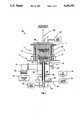
- FIG. 1is a schematic diagram showing an axial cross-sectional view of one embodiment of the plasma generating apparatus of this invention, particularly illustrating a dual plasma source including an initiating ECR microwave plasma 4 and an acting radio-frequency plasma 5;
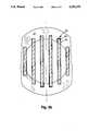
- FIG. 2ais an axial cross-sectional view of a magnetic filter used to couple the two plasmas in the apparatus of FIG. 1 and FIG. 3, the magnetic filter including magnets and electrically biased slotted plates for assisting the production of large uniform plasmas at low pressures;
- FIG. 2bis a transverse cross-sectional view of the magnetic filter of FIG. 2a.
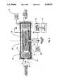
- FIG. 3is a schematic diagram showing an axial cross-sectional view of an alternative dual plasma source for plasma processing of the invention, particularly illustrating a parallel plate geometry featuring a peripheral initiating ECR microwave plasma 90 and an acting radio-frequency plasma 91.
- a plasma source 10featuring two physically separated but coupled plasmas 4 and 5 is described.
- the sourcegenerates a uniform plasma over a large area of about 1000 cm 2 at low pressures below 0.1 mtorr.
- a cylindrical vacuum chamber 60has a pumping region located below the substrate (workpiece) 40 and RF powered substrate holder 41, an upper region where an initiating ECR microwave plasma 4 is generated, and a parallel plate mid region where the radio-frequency (RF) plasma 5 that acts on the substrate 40 is formed.
- the two plasmasmay be operated independently.
- the ECR microwave multicusp plasma source 11may use 2.45 GHz microwaves, while the radio-frequency parallel plate plasma generator 12 may be excited with RF at 13.56 MHz, for example.
- the electron cyclotron resonance (ECR) microwave multicusp plasma source 11 of Tsai(U. S. Pat. 5,032,202) has been developed to produce plasmas of argon, helium, hydrogen, oxygen, etc., at operating pressures in the range from 0.1 to 10 mtorr.
- ECR microwave multicusp plasma sourcesare known to operate at desired low pressures compared to RF parallel plate plasma generators that typically operate above 100 mtorr and with much difficulty at pressures below 1 mtorr.
- the subject inventionis a coupled plasma, dual radio-frequency (13.56 MHz) and microwave (2.45 GHz) plasma source that produces a uniform plasma over a large substrate at low pressure with a high fraction of ionization of the cold working gas particles.
- the ECR microwave multicusp plasma source 11is used to initiate the discharge of the acting plasma 5. Electrons in the ECR microwave plasma 4 drift through the magnetic filter 13 into the RF chamber to initiate and feed the RF plasma 5.
- the magnetic filter 13is designed to control microwave entry into the RF plasma region and to enhance reliability and uniformity of the RF discharge at low pressures.
- microwave energyis used to accelerate electrons, which excite and ionize working gas particles and produce an ECR microwave plasma 4.
- the microwave energyenters the source 11 through a conventional microwave waveguide 20 and microwave entrance window 21.
- the magnetic filter 13includes magnet column assemblies 31 mounted in a metal ring 37, upper slotted plate 30, lower slotted plate 32, and post insulators 38 between these components for electrical separation.
- Power supplies 47, 48, and 49are used to bias the plate 32, ring 37 and plate 30, respectively.
- the upper slotted plate 30 facing the ECR microwave plasma 4is biased negatively for producing microwave plasmas at low pressures.
- the lower slotted plate 32 facing the RF plasma 5is biased positively to accelerate electrons which diffuse from the ECR microwave plasma 4 into the RF plasma 5 through the slot regions between the magnet columns 31.
- the ring 37 with its associated magnet column assemblies 31are biased positively with respect to ground to control electron and ion energy distributions.
- the placement of the magnet columns and the polarity of the power suppliescan be optimized for achieving particular plasma properties in the associated application.
- the magnet columns 31 of FIG. 2aare assembled by placing strong magnets 35 on a thin soft iron bar 36 where they are held in place by magnetic attraction. When all the magnets are thus placed, the bar magnet assembly is enclosed in an aluminum casing 34.
- the magnet column assemblies 31may be press-fit into slots in the metal ring 37 to form a magnetic field of desired configuration in the vacuum chamber 60.
- the magnetic filter 13may be installed in the chamber 60 using ring insulators 39 that electrically insulate it from the two plasma regions.
- the materials chosen for constructing the coupled plasma sourceshould be relatively inert to the processing gas and plasmas, and be free of impurities generation. Stainless steel, quartz, and anodized aluminum are typical materials of construction.
- the magnetsmay be samarium cobalt magnets.
- the lower limit of operating pressureis extended further by use of proper plasma confining line cusp magnetic field design in both the ECR microwave plasma 4 region and in the RF plasma 5 region.
- the enclosing static magnetic fieldis due to magnet columns 25, 26 in the source 11, magnet columns 27 in the source 12, and bar magnets 35 in the magnetic filter 13.
- the lower slotted plate 32 facing the RF plasma 5is biased positively to accelerate electrons diffusing through the slot regions between magnet columns. These electrons gain further energy from the applied RF fields in both the ECR zone 8 and the plasma sheath region, i.e., the region of plasma 5 adjacent the powered substrate holder 41.
- the magnetic columns 27 located on the chamber 60 wall in the region of the RF plasma generator 12 in combination with the magnetic filter 13form the second ECR zone 8, which is used to contain electrons in the RF plasma 5 and enhance the RF discharge. Utilizing the confined high energy electrons and increased lifetime, the electrons improve the ionization efficiency and produce plasmas at lower pressures. Thus, the lower limit of the source operating pressure can be extended below 0.1 mtorr.
- RF energyis supplied to the RF plasma generator 12 from the commercial RF supply 55.
- the RF energypasses through the tuning circuit 56, RF coaxial cable 57, and RF feedthrough 54 to a metal tube 59.
- the tuning circuit 56is an impedance matching circuit which, in simplest form, may be only a capacitor.
- the metal tube 59terminates at the substrate holder 41 to provide the active element, or electrode of the RF parallel plate plasma generator 12.
- An electrically insulating pyre tube 58surrounds the metal tube 59. Together, these tubes and mechanical vacuum feedthrough 53 function as a vertically adjustable support pedestal for the substrate holder 41. Insulators 42 isolate the powered substrate holder 41 from its supporting frame 43 inside the pumping region of vacuum chamber 60.
- Working gas from a source 61passes through vacuum feedthrough 53 and into the RF plasma generator 12 through the metal tube 59.
- the gas feeds 28, 61can be operated independently of each other.
- the gas pressure in the vacuum chamber 60is varied by controlling the gas pumping and the gas feeds, and regulating the vacuum valve 50 between the vacuum piping 51 and the turbomolecular vacuum pump 52.
- the dual plasma source 10can be operated to produce only an ECR microwave plasma 4, only an RF plasma 5, or, in preferred embodiment, coupled plasmas 4 and 5 simultaneously.
- the dual sourceIn order to produce a large and uniform RF plasma 5 at low pressures below 0.1 mtorr, the dual source must be operated in the coupled plasma mode.
- a further feature of the dual plasma sourceis that the RF plasma 5, uniform over the substrate 40, is very readily produced.
- the dual sourceis very flexible for producing various plasmas for various plasma processing applications.
- the RF poweris applied between the substrate holder 41 and the magnetic filter 13 by means of the RF supply 55 and biasing supplies 47-49.
- the RF powerwould be applied through the filter 13 while the substrate holder 41 would be grounded.
- the source shown in FIG. 1is operated for etching as follows. First, the vacuum chamber is pumped down with the vacuum system to establish the proper vacuum conditions, that is, the proper gas pressure and gas throughput through the system. The gas feed system and throttling valve 50 near the vacuum pump are used to accomplish this. After the gas pressure and gas throughput are established, the source power supplies are warmed up for the feed of the microwaves into the source 11 via the Waveguide 20 and window 21. At the same time, a choice of biasing parameters is made for the magnetic filter 13, and these parameters are a priori set at the power supplies 47-49.
- the ECR microwave plasmais established without much regard to the RF plasma generation.
- microwave poweris introduced into the vacuum chamber.
- the microwavesbounce around.
- electronsgain energy from microwave fields to initiate discharges in the plasma regions 4, 5.
- the electrons heated in specific resonant zones 7-9are confined by the cusp fields and aid in the formation of the uniform plasmas 4 and 5.
- the magnets 25-27 and 35provide two functions; they provide the resonant zones for the microwaves for the heating of electrons, and they provide the plasma confinement.
- the next taskis to vary the potentials on the filter region at the power supplies 47-49.
- the ion and electron density in the RF plasma 5 regionis measured, either by a probe or by monitoring the current on the substrate holder 41. This may be done by placing a potential on the substrate holder 41, statically at first, then negative and positive, varying them to understand what kind of plasma is being created in the RF region. By an external mechanism such as a probe in the RF plasma region, the plasma variations resulting from placing the RF potential on the workpiece holder are then determined.
- the applied microwave power, pressure, electrical potentials on the magnetic filter 13, and RF potentials on the workpiece holder 41are varied until the desired plasma uniformity, density, ion energy, and electron energy parameters are attained.
- the workpiece holdermay be moved up and down in the vacuum chamber to take advantage of the most uniform plasma location. Of course, this may also require subsequent iteration of the parameters mentioned before.
- FIG. 3illustrates an alternate version of the dual plasma source. Like the source of FIG. 1, it utilizes an ECR microwave plasma initiating and feeding an RF plasma; the construction of the vacuum chamber and use of the magnetic filter is different.
- the vacuum chamber 72is again cylindrical. It has an outer peripheral region for forming a circumferential ECR microwave plasma 90 and an inner parallel plate region for forming the RF plasma 91.
- the source pressureis controlled by gas pumping and the working gas feeds 70 and 82 to the plasma 90, 91 regions, respectively.
- the ECR microwave plasma 90is produced in the chamber 72 by applying microwave power via the microwave waveguide 74 and microwave entrance window 71 into the ECR microwave plasma region.
- One or more microwave feedsmay be needed to fill the peripheral region with microwaves.
- Magnet columns 73are placed around the vacuum chamber 72 walls in the region of the plasma 90. As before, electrons in the region are accelerated by the microwave electric field, ionize working gas particles, and produce an ECR zone 84 for the ECR microwave plasma 90. Electrons from the plasma 90 diffuse through the magnetic filter 75, enter the RF plasma 91 region, and initiate an RF discharge between the parallel plates 80 and 81.
- the magnetic filter 75is similar to the one shown and described in the embodiment of FIG. 1.
- the RF electric field from the RF supply 77 and tuning circuit 76is applied between the substrate holder 81 and parallel plate 80.
- the electrons in the RF plasma 91 regionare accelerated, ionize the working gas particles, and form the ECR zone 85 from which the RF plasma 91 is produced.
- the ECR zone 85forms due to the nearby static magnetic field from the magnetic filter 75 and magnet columns 83 located on parallel plate 80.
- the RF poweris applied to the substrate holder 81 on which the substrate is fastened, and the parallel plate 80 is the grounded electrode.
- the RF poweris applied to the parallel plate 80, while the substrate holder 81, on which the working piece is fastened, would be grounded.
- the RF plasma 91is formed between plates 80 and 81 similar to a parallel plate reactor.
- the RF plasma 5is formed between the magnetic filter 13 and powered substrate holder 41, both together functioning in the manner of two parallel plates.
- the plasma source of FIG. 3is also capable of operating at low pressures of 0.1 mtorr and below.
- the source of FIG. 3is operated for etching like that of FIG. 1.
- the microwavesbounce around in the plasma 90, 91 regions.
- the ECR microwave plasma 90is formed in the outer peripheral region of the vacuum chamber 72. Electrons gain energy from microwaves applied in the ECR zone 84 and produce this plasma at very low pressure, below 0.1 mtorr. With the plasma 90 created, the plasma electrons pass through the magnetic filter 75 into the RF plasma 91 region. The electrons gain further energy from 1) microwaves that are introduced through the filter 75, 2) the ECR resonance zone 85, and 3) RF power applied to the substrate holder 81. The uniform RF plasma is then used for plasma etching on the substrate.
- the coupled plasma sourcesare expected to operate as reliably as the ECR microwave plasma source of prior invention at low pressures of 0.1mtorr.
- the sourcesprovide the flexibility of control of plasma current density and variable ion energy desired for materials processing.
- the plasma sourcesare designed with magnetic multicusp configurations that closely confine both of the coupled plasmas.
- the plasma sourcescan be configured with various other geometries, e.g. sphere, cylinder, tube, etc.
- the physical separation of the two dischargesenhances the flexibility for performing etching and deposition processes. It allows large plasma reactors to be designed for mass production.
- the alternative design of FIG. 3can also be used for both etching and deposition applications.
- Magnetic filterimproves the discharge stability and plasma confinement of both embodiment of the invention, and reduces the plasma impurity content from the chamber walls.
- the capability to perform plasma deposition at low pressurereduces impurity clusters. Impurity clusters form in the gas phase, deposit as thin films, degrade the quality of the process, and damage substrate films. Improvement in plasma confinement and reduction in impurity content enhances the operating efficiency of the plasma reactor.
- the magnetic configuration in the magnetic filtercan be designed to perform particular etching or deposition applications, controlling charged or neutral particles that pass through the magnetic filter from the ECR microwave plasma 4 to the RF plasma 5.
- the magnetic filterprovides independent electrical biasing of the slotted plates 30 and 32 and the magnet assemblies 31 both in magnitude and in polarity to control properties of the RF plasma for special etching and deposition applications.
- This inventionprovides for independent control of operating parameters in the target region such as gas pressure, gas species, microwave power, microwave frequency, RF frequency, and RF power.
- the sourcesprovide simple mechanical structures for producing uniform plasmas at low pressures.
- the sourcesuses ECR microwave plasmas to initiate RF discharges and produce uniform plasmas between RF parallel plates for manufacturing microelectronics.
Landscapes
- Physics & Mathematics (AREA)
- Engineering & Computer Science (AREA)
- Plasma & Fusion (AREA)
- Chemical & Material Sciences (AREA)
- Analytical Chemistry (AREA)
- Plasma Technology (AREA)
- Chemical Vapour Deposition (AREA)
Abstract
Description
This invention was made with Government support under contract no. DE-AC05-84OR21400 awarded by the U. S. Department of Energy. The Government has certain rights in this invention.
1. Technical Field
This invention relates generally to vacuum deposition and etching apparatus, and more particularly to a plasma source utilizing coupled ECR microwave and radio-frequency (RF) plasmas; the apparatus particularly employing line cusp magnetic multipole structures in both plasma regions for enhancing plasma confinement and producing a uniform plasma over a large substrate area, and also incorporating an electrically-biased magnetic filter for controlling the properties of the ECR microwave and RF plasmas.
2. Prior Art
In U. S. Pat. No. 5,032,202, one of the inventors provided an improved ECR microwave plasma source featuring a magnetic multipole construction for both the plasma confinement and plasma generation, and which also provides a uniform plasma for large area plasma processing. Like ECR microwave plasma sources before it, the plasma source relies solely on microwave energy to produce its plasma. In microwave plasma sources, variations of the plasma uniformity are a sensitive function of gas pressure and magnetic field in the microwave launcher.
Parallel plate radio-frequency (RF) reactors are another type of vacuum deposition and etching apparatus. See, for example, C. M. Melliar-Smith and C. J. Mogab, "Plasma-Assisted Etching Techniques for Pattern Delineation", in Thin Film Processes (J. L. Vossen and W. Kern, Eds.), Academic Press, New York, Chapt. V-2 (1978) pp.497-556. It is well known with parallel plate radio-frequency (RF) reactors that it is difficult to produce desired high density and uniform plasma at low pressures below 1 mtorr. Low pressures are desired to minimize gas scattering because the uniformity and directionality become more important as the sub-features are reduced in size for manufacturing of the electronics.
Recently, the use of electron cyclotron resonance (ECR) modes and static magnetic field structures have been reported in connection with parallel plate RF reactors (U. S. Pat. Nos. 4,585,668; 4,630,566; 4,691,662; 4,727,293; 4,906,900; and 5,081,398).
In one of these pats. 4,691,662, Roppel et al feeds charged excited species to the active RF plasma from a physically separated ECR microwave disk plasma. Roppel characterizes his active plasma as a microwave and RF plasma (or hybrid plasma) since it includes species from both microwave excitation and RF excitation. Roppel was able to achieve flexibility by controlling reactive species of the hybrid plasma. However, the operating pressure range was not reported The plasma source appears to operate at pressures well above 1 mtorr because of limited magnetic confinement for both the disk microwave plasma and the hybrid plasma. In fact, FIG. 1 of the 4,691,662 patent depicts some of themagnets 20 located on the sliding plate of the microwave cavity. In the Roppel apparatus, a resonant cavity is used to induce strong microwave electric fields which in turn create the microwave driven plasma inside a quartz dish. In such a source, the frequency required of the power supply decreases inversely proportional to the cross-sectional area of the microwave plasma. Consequently, it is difficult in such a source to create a uniform plasma over a large article at low pressures below 0.1 mtorr as needed for manufacturing microelectronics.
Accordingly, it is a first object of this invention to use an ECR microwave plasma discharge to feed and initiate an RF discharge in a parallel plate reactor to produce a desired uniform high density plasma at low pressures below 0.1 mtorr.
Another object of the invention is to couple an ECR microwave plasma to an RF plasma in a manner that produces a plasma with improved properties for uniformly treating substrates with large areas.
Another object is to provide an electrically-biased magnetic filter between an ECR microwave plasma discharge and an RF plasma discharge for achieving both operational reliability and plasma uniformity at low pressures.
Still another object is to enhance the flexibility of plasma processing at low pressures by providing a magnetic filter with variable microwave passage and operating with controllable electrical biasing.
Yet another object of this invention is to enhance flexibility of operating over a wide parameter space thereby allowing investigation of design parameters that influence plasmas processing applications.
Another object is to provide a large-area ECR microwave plasma source that is capable of being scaled up in size with minimum effort, thereby simplifying the design of large area ECR microwave and RF plasma reactors.
Yet another object of this invention is to provide an improved dual plasma reactor featuring magnetically enhanced plasma generation for material processing.
Further and other objects and advantages of the present invention will become apparent from the description contained herein.
A plasma processor incorporating an electron cyclotron resonance (ECR) microwave plasma source to initiate and feed the radio-frequency (RF) plasma of a RF plasma source in a common vacuum chamber is improved as follows:
the microwave plasma source includes static magnetic field producing means located at the walls of the microwave source for producing an ECR zone over a maximum extent of inner wall area, the microwave source operating at ECR and producing a uniform ECR microwave plasma over at least a 1000 cm2 area at a pressure below 0.1 mtorr;
the RF plasma source includes static magnetic field means for producing ECR zones within the RF plasma source; and
a magnetic filter is used between the plasma sources, the filter including static magnetic field means and electrically biased plates for affecting the ECR microwave plasma and RF plasma;
the static magnetic field means of the filter also producing ECR zones within the ECR microwave plasma source and the RF plasma source.
In the drawings:
FIG. 1 is a schematic diagram showing an axial cross-sectional view of one embodiment of the plasma generating apparatus of this invention, particularly illustrating a dual plasma source including an initiatingECR microwave plasma 4 and an acting radio-frequency plasma 5;
FIG. 2a is an axial cross-sectional view of a magnetic filter used to couple the two plasmas in the apparatus of FIG. 1 and FIG. 3, the magnetic filter including magnets and electrically biased slotted plates for assisting the production of large uniform plasmas at low pressures;
FIG. 2b is a transverse cross-sectional view of the magnetic filter of FIG. 2a; and
FIG. 3 is a schematic diagram showing an axial cross-sectional view of an alternative dual plasma source for plasma processing of the invention, particularly illustrating a parallel plate geometry featuring a peripheral initiatingECR microwave plasma 90 and an acting radio-frequency plasma 91.
For a better understanding of the present invention, together with other and further objects, advantages, and capabilities thereof, reference is made to the following disclosure and appended claims in connection with the above-described drawings.
In FIG. 1, aplasma source 10 featuring two physically separated but coupledplasmas cylindrical vacuum chamber 60 has a pumping region located below the substrate (workpiece) 40 and RF poweredsubstrate holder 41, an upper region where an initiatingECR microwave plasma 4 is generated, and a parallel plate mid region where the radio-frequency (RF)plasma 5 that acts on thesubstrate 40 is formed. The two plasmas may be operated independently. The ECR microwavemulticusp plasma source 11 may use 2.45 GHz microwaves, while the radio-frequency parallelplate plasma generator 12 may be excited with RF at 13.56 MHz, for example.
The electron cyclotron resonance (ECR) microwavemulticusp plasma source 11 of Tsai (U. S. Pat. 5,032,202) has been developed to produce plasmas of argon, helium, hydrogen, oxygen, etc., at operating pressures in the range from 0.1 to 10 mtorr. Thus, ECR microwave multicusp plasma sources are known to operate at desired low pressures compared to RF parallel plate plasma generators that typically operate above 100 mtorr and with much difficulty at pressures below 1 mtorr. Thus, the subject invention is a coupled plasma, dual radio-frequency (13.56 MHz) and microwave (2.45 GHz) plasma source that produces a uniform plasma over a large substrate at low pressure with a high fraction of ionization of the cold working gas particles.
Again in FIG. 1, the ECR microwavemulticusp plasma source 11 is used to initiate the discharge of the actingplasma 5. Electrons in theECR microwave plasma 4 drift through themagnetic filter 13 into the RF chamber to initiate and feed theRF plasma 5. Themagnetic filter 13 is designed to control microwave entry into the RF plasma region and to enhance reliability and uniformity of the RF discharge at low pressures. In further detail, in thesource 11, microwave energy is used to accelerate electrons, which excite and ionize working gas particles and produce anECR microwave plasma 4. The microwave energy enters thesource 11 through aconventional microwave waveguide 20 andmicrowave entrance window 21.
It will be noted that in Tsai's earlier pat. (5,032,202), a magnet coil/microwave launcher surrounded the microwave window, and magnetic columns surrounded the chamber walls. Such structure resulted in two ECR zones, one in the throat of the microwave launcher and the other at the periphery of the chamber. In the present invention,magnet columns 25 cover the top ofchamber 60 and replace the former magnet coil and microwave launcher. This has the result, shown in FIG. 1, of producing asingle ECR zone 7 around the entire inner periphery of the ECR microwavemulticusp plasma source 11. As in the earlier source, microwave energy in theECR zone 7 accelerates electrons and produces theECR microwave plasma 4. The electrons in theECR microwave plasma 4 subsequently diffuse through themagnetic filter 13 and initiate RF discharges that produce theRF plasma 5 in the (mid) region between themagnetic filter 13 andpowered substrate holder 41.
Now in FIGS. 2a and 2b, themagnetic filter 13 includesmagnet column assemblies 31 mounted in ametal ring 37, upper slottedplate 30, lower slottedplate 32, and postinsulators 38 between these components for electrical separation. Power supplies 47, 48, and 49 are used to bias theplate 32,ring 37 andplate 30, respectively. In the example of FIG. 2a, the upper slottedplate 30 facing theECR microwave plasma 4 is biased negatively for producing microwave plasmas at low pressures. The lower slottedplate 32 facing theRF plasma 5 is biased positively to accelerate electrons which diffuse from theECR microwave plasma 4 into theRF plasma 5 through the slot regions between themagnet columns 31. Thering 37 with its associatedmagnet column assemblies 31 are biased positively with respect to ground to control electron and ion energy distributions. The placement of the magnet columns and the polarity of the power supplies can be optimized for achieving particular plasma properties in the associated application.
Themagnet columns 31 of FIG. 2a are assembled by placingstrong magnets 35 on a thinsoft iron bar 36 where they are held in place by magnetic attraction. When all the magnets are thus placed, the bar magnet assembly is enclosed in analuminum casing 34. Themagnet column assemblies 31 may be press-fit into slots in themetal ring 37 to form a magnetic field of desired configuration in thevacuum chamber 60. In practice, themagnetic filter 13 may be installed in thechamber 60 usingring insulators 39 that electrically insulate it from the two plasma regions. For plasma processing applications, the materials chosen for constructing the coupled plasma source should be relatively inert to the processing gas and plasmas, and be free of impurities generation. Stainless steel, quartz, and anodized aluminum are typical materials of construction. The magnets may be samarium cobalt magnets.
In the invention, the lower limit of operating pressure is extended further by use of proper plasma confining line cusp magnetic field design in both theECR microwave plasma 4 region and in theRF plasma 5 region. The enclosing static magnetic field is due tomagnet columns source 11,magnet columns 27 in thesource 12, andbar magnets 35 in themagnetic filter 13. As mentioned previously, the lower slottedplate 32 facing theRF plasma 5 is biased positively to accelerate electrons diffusing through the slot regions between magnet columns. These electrons gain further energy from the applied RF fields in both theECR zone 8 and the plasma sheath region, i.e., the region ofplasma 5 adjacent thepowered substrate holder 41. These energetic electrons are reflected by, bounced off of, and contained by the electric and magnetic fields adjacent the RF parallel plates (holder 41 and filter 13) andchamber 60 walls. These energetic electrons ionize the working gas particles and create theRF plasma 5. Because the ECR microwavemulticusp plasma source 11 in combination with themagnetic filter 13 distributes the ionizing electrons uniformly over the whole RF discharge chamber area, theRF plasma 5 is likewise uniform, resulting in very uniform processing of thesubstrate 40.
As mentioned previously, themagnetic columns 27 located on thechamber 60 wall in the region of theRF plasma generator 12 in combination with themagnetic filter 13 form thesecond ECR zone 8, which is used to contain electrons in theRF plasma 5 and enhance the RF discharge. Utilizing the confined high energy electrons and increased lifetime, the electrons improve the ionization efficiency and produce plasmas at lower pressures. Thus, the lower limit of the source operating pressure can be extended below 0.1 mtorr.
Again in FIG. 1, RF energy is supplied to theRF plasma generator 12 from thecommercial RF supply 55. The RF energy passes through thetuning circuit 56, RFcoaxial cable 57, and RF feedthrough 54 to ametal tube 59. Thetuning circuit 56 is an impedance matching circuit which, in simplest form, may be only a capacitor. Themetal tube 59 terminates at thesubstrate holder 41 to provide the active element, or electrode of the RF parallelplate plasma generator 12. An electrically insulatingpyre tube 58 surrounds themetal tube 59. Together, these tubes andmechanical vacuum feedthrough 53 function as a vertically adjustable support pedestal for thesubstrate holder 41.Insulators 42 isolate thepowered substrate holder 41 from its supportingframe 43 inside the pumping region ofvacuum chamber 60. Working gas from asource 61 passes throughvacuum feedthrough 53 and into theRF plasma generator 12 through themetal tube 59. The gas feeds 28, 61 can be operated independently of each other. The gas pressure in thevacuum chamber 60 is varied by controlling the gas pumping and the gas feeds, and regulating thevacuum valve 50 between the vacuum piping 51 and theturbomolecular vacuum pump 52. With independent control of the applied microwave and RF powers, thedual plasma source 10 can be operated to produce only anECR microwave plasma 4, only anRF plasma 5, or, in preferred embodiment, coupledplasmas uniform RF plasma 5 at low pressures below 0.1 mtorr, the dual source must be operated in the coupled plasma mode. A further feature of the dual plasma source is that theRF plasma 5, uniform over thesubstrate 40, is very readily produced. Clearly, the dual source is very flexible for producing various plasmas for various plasma processing applications.
For etching applications, the RF power is applied between thesubstrate holder 41 and themagnetic filter 13 by means of theRF supply 55 and biasing supplies 47-49. For deposition applications, the RF power would be applied through thefilter 13 while thesubstrate holder 41 would be grounded.
The source shown in FIG. 1 is operated for etching as follows. First, the vacuum chamber is pumped down with the vacuum system to establish the proper vacuum conditions, that is, the proper gas pressure and gas throughput through the system. The gas feed system and throttlingvalve 50 near the vacuum pump are used to accomplish this. After the gas pressure and gas throughput are established, the source power supplies are warmed up for the feed of the microwaves into thesource 11 via theWaveguide 20 andwindow 21. At the same time, a choice of biasing parameters is made for themagnetic filter 13, and these parameters are a priori set at the power supplies 47-49.
Next, the ECR microwave plasma is established without much regard to the RF plasma generation. Using some relatively low pressure and low microwave feed, microwave power is introduced into the vacuum chamber. Upon entering the chamber, the microwaves bounce around. At specific resonant zones 7-9 as determined by the magnetic fields surrounding the chamber, electrons gain energy from microwave fields to initiate discharges in theplasma regions uniform plasmas
The next task is to vary the potentials on the filter region at the power supplies 47-49. During this step, the ion and electron density in theRF plasma 5 region is measured, either by a probe or by monitoring the current on thesubstrate holder 41. This may be done by placing a potential on thesubstrate holder 41, statically at first, then negative and positive, varying them to understand what kind of plasma is being created in the RF region. By an external mechanism such as a probe in the RF plasma region, the plasma variations resulting from placing the RF potential on the workpiece holder are then determined.
Next, the applied microwave power, pressure, electrical potentials on themagnetic filter 13, and RF potentials on theworkpiece holder 41 are varied until the desired plasma uniformity, density, ion energy, and electron energy parameters are attained. There remains one further parameter for plasma control. Since the plasma uniformity over the substrate holder is a complicated result of the parameters mentioned, the workpiece holder may be moved up and down in the vacuum chamber to take advantage of the most uniform plasma location. Of course, this may also require subsequent iteration of the parameters mentioned before.
It will be understood that the particular static magnetic field configurations used in this invention improve the efficiency of plasma generation in bothplasma regions regions
FIG. 3 illustrates an alternate version of the dual plasma source. Like the source of FIG. 1, it utilizes an ECR microwave plasma initiating and feeding an RF plasma; the construction of the vacuum chamber and use of the magnetic filter is different. In this source, thevacuum chamber 72 is again cylindrical. It has an outer peripheral region for forming a circumferentialECR microwave plasma 90 and an inner parallel plate region for forming theRF plasma 91. As before, the source pressure is controlled by gas pumping and the working gas feeds 70 and 82 to theplasma ECR microwave plasma 90 is produced in thechamber 72 by applying microwave power via themicrowave waveguide 74 andmicrowave entrance window 71 into the ECR microwave plasma region. One or more microwave feeds may be needed to fill the peripheral region with microwaves.
The RF electric field from theRF supply 77 andtuning circuit 76 is applied between thesubstrate holder 81 andparallel plate 80. The electrons in theRF plasma 91 region are accelerated, ionize the working gas particles, and form theECR zone 85 from which theRF plasma 91 is produced. TheECR zone 85 forms due to the nearby static magnetic field from themagnetic filter 75 andmagnet columns 83 located onparallel plate 80.
For etching applications, the RF power is applied to thesubstrate holder 81 on which the substrate is fastened, and theparallel plate 80 is the grounded electrode. For deposition applications, the RF power is applied to theparallel plate 80, while thesubstrate holder 81, on which the working piece is fastened, would be grounded.
It will be noted in FIG. 3 that theRF plasma 91 is formed betweenplates RF plasma 5 is formed between themagnetic filter 13 andpowered substrate holder 41, both together functioning in the manner of two parallel plates. With the improvement in electron confinement achieved by use of themagnet columns magnetic filter 75, the plasma source of FIG. 3 is also capable of operating at low pressures of 0.1 mtorr and below.
The source of FIG. 3 is operated for etching like that of FIG. 1. The microwaves bounce around in theplasma ECR microwave plasma 90 is formed in the outer peripheral region of thevacuum chamber 72. Electrons gain energy from microwaves applied in theECR zone 84 and produce this plasma at very low pressure, below 0.1 mtorr. With theplasma 90 created, the plasma electrons pass through themagnetic filter 75 into theRF plasma 91 region. The electrons gain further energy from 1) microwaves that are introduced through thefilter 75, 2) theECR resonance zone 85, and 3) RF power applied to thesubstrate holder 81. The uniform RF plasma is then used for plasma etching on the substrate.
Some of the major features and advantages of the coupled plasma sources of the invention are described below:
1. Reliability. The coupled plasma sources are expected to operate as reliably as the ECR microwave plasma source of prior invention at low pressures of 0.1mtorr. The sources provide the flexibility of control of plasma current density and variable ion energy desired for materials processing.
2. Efficiency. The plasma sources are designed with magnetic multicusp configurations that closely confine both of the coupled plasmas.
3. Configuration. The plasma sources can be configured with various other geometries, e.g. sphere, cylinder, tube, etc. In the version of FIG. 1, the physical separation of the two discharges enhances the flexibility for performing etching and deposition processes. It allows large plasma reactors to be designed for mass production. The alternative design of FIG. 3 can also be used for both etching and deposition applications.
4. Magnetic filter. The magnetic filter improves the discharge stability and plasma confinement of both embodiment of the invention, and reduces the plasma impurity content from the chamber walls. The capability to perform plasma deposition at low pressure reduces impurity clusters. Impurity clusters form in the gas phase, deposit as thin films, degrade the quality of the process, and damage substrate films. Improvement in plasma confinement and reduction in impurity content enhances the operating efficiency of the plasma reactor. Moreover, the magnetic configuration in the magnetic filter can be designed to perform particular etching or deposition applications, controlling charged or neutral particles that pass through the magnetic filter from theECR microwave plasma 4 to theRF plasma 5. In addition to providing magnetic biasing, the magnetic filter provides independent electrical biasing of the slottedplates magnet assemblies 31 both in magnitude and in polarity to control properties of the RF plasma for special etching and deposition applications.
5. Flexibility. This invention provides for independent control of operating parameters in the target region such as gas pressure, gas species, microwave power, microwave frequency, RF frequency, and RF power.
6. Simplicity. The sources provide simple mechanical structures for producing uniform plasmas at low pressures.
7. Dual source. The sources uses ECR microwave plasmas to initiate RF discharges and produce uniform plasmas between RF parallel plates for manufacturing microelectronics.
8. Operation Increased microwave introduction into the rf plasma generator enhances the rf discharge. Reduced microwave power in the RF plasma region reduces the risks of damage to the microfeatures being processed.
While there has been shown and described what are at present considered the preferred embodiments of the invention, it will be obvious to those skilled in the art that various changes and modifications can be made therein without departing from the scope of the inventions defined by the appended claims.
Claims (8)
1. In a plasma processor incorporating an electron cyclotron resonance (ECR) microwave plasma source to initiate and feed the radio-frequency (RF) plasma of a RF plasma source in a common vacuum chamber, the improvement comprising:
said microwave plasma source including static magnetic field producing means located at the walls of said microwave source for producing an ECR zone over a maximum extent of inner wall area, said microwave source operating at ECR and producing a uniform ECR microwave plasma over at least a 1000 cm2 area at a pressure below 0.1 mtorr;
said RF plasma source including static magnetic field means for producing ECR zones within said RF plasma source; and
a magnetic filter between said plasma sources, said filter including static magnetic field means and electrically biased plates for affecting said ECR microwave plasma and said RF plasma;
said static magnetic field means of said filter also producing ECR zones within said ECR microwave plasma source and said RF plasma source.
2. In the plasma processor of claim 1, the walls of said microwave plasma source and said RF plasma source being right circular cylindrical;
said magnetic filter having a right circular cylindrical geometry; and
said ECR microwave plasma source, said magnetic filter, and said RF plasma source being arranged along a common axis.
3. In the plasma processor of claim 1, said RF plasma source being right circular cylindrical;
said magnetic filter having a circumferential geometry, and being disposed coaxially about said RF plasma source; and
said ECR microwave plasma source having a circumferential geometry, and being disposed coaxially about said magnetic filter.
4. A plasma processor according to claim 3 further including a second ECR microwave plasma source, the walls of said second ECR microwave plasma source being right circular cylindrical, said plasma processor and said second ECR microwave plasma source being arranged along a common axis, and said second ECR microwave plasma source providing a second microwave feed into said RF plasma source for added flexibility in plasma processing.
5. In the plasma processor of claim 1, said magnetic filter including bar-shaped magnet column assemblies mounted in a metal ring, said metal ring disposed between two slotted plates, said ring and said slotted plates being capable of independent electrical biasing through individual power supplies.
6. The plasma processor of claim 1 wherein said microwave plasma source is turned on and said RF plasma source is turned off.
7. The plasma processor of claim 1 wherein said microwave plasma source is turned off and said RF plasma source is turned on.
8. The plasma processor of claim 1 wherein said microwave plasma source is turned on and said RF plasma source is turned on.
Priority Applications (1)
| Application Number | Priority Date | Filing Date | Title |
|---|---|---|---|
| US07/930,590US5292370A (en) | 1992-08-14 | 1992-08-14 | Coupled microwave ECR and radio-frequency plasma source for plasma processing |
Applications Claiming Priority (1)
| Application Number | Priority Date | Filing Date | Title |
|---|---|---|---|
| US07/930,590US5292370A (en) | 1992-08-14 | 1992-08-14 | Coupled microwave ECR and radio-frequency plasma source for plasma processing |
Publications (1)
| Publication Number | Publication Date |
|---|---|
| US5292370Atrue US5292370A (en) | 1994-03-08 |
Family
ID=25459495
Family Applications (1)
| Application Number | Title | Priority Date | Filing Date |
|---|---|---|---|
| US07/930,590Expired - Fee RelatedUS5292370A (en) | 1992-08-14 | 1992-08-14 | Coupled microwave ECR and radio-frequency plasma source for plasma processing |
Country Status (1)
| Country | Link |
|---|---|
| US (1) | US5292370A (en) |
Cited By (211)
| Publication number | Priority date | Publication date | Assignee | Title |
|---|---|---|---|---|
| US5413954A (en)* | 1992-11-10 | 1995-05-09 | At&T Bell Laboratories | Method of making a silicon-based device comprising surface plasma cleaning |
| US5527396A (en)* | 1992-06-30 | 1996-06-18 | Canon Kabushiki Kaisha | Deposited film forming apparatus |
| US5620522A (en)* | 1994-09-30 | 1997-04-15 | Hitachi, Ltd. | Microwave plasma generator |
| US5651825A (en)* | 1994-03-02 | 1997-07-29 | Nissin Electric Co., Ltd. | Plasma generating apparatus and plasma processing apparatus |
| US5707452A (en)* | 1996-07-08 | 1998-01-13 | Applied Microwave Plasma Concepts, Inc. | Coaxial microwave applicator for an electron cyclotron resonance plasma source |
| US5735451A (en)* | 1993-04-05 | 1998-04-07 | Seiko Epson Corporation | Method and apparatus for bonding using brazing material |
| US5753886A (en)* | 1995-02-07 | 1998-05-19 | Seiko Epson Corporation | Plasma treatment apparatus and method |
| US5758680A (en)* | 1996-03-29 | 1998-06-02 | Lam Research Corporation | Method and apparatus for pressure control in vacuum processors |
| US5783102A (en)* | 1996-02-05 | 1998-07-21 | International Business Machines Corporation | Negative ion deductive source for etching high aspect ratio structures |
| US5803107A (en)* | 1996-03-29 | 1998-09-08 | Lam Research Corporation | Method and apparatus for pressure control in vacuum processors |
| US5831238A (en)* | 1993-12-09 | 1998-11-03 | Seiko Epson Corporation | Method and apparatus for bonding using brazing material at approximately atmospheric pressure |
| US5835996A (en)* | 1995-12-18 | 1998-11-10 | Seiko Epscon Corporation | Power generation method and power generator using a piezoelectric element, and electronic device using the power |
| US5858162A (en)* | 1993-01-29 | 1999-01-12 | Sony Corporation | Plasma processing apparatus |
| EP0749147A3 (en)* | 1995-06-13 | 1999-01-13 | Ipsen International GmbH | Method and device for controlling the electrical current density over a workpiece during heat treatment by plasma |
| US5918354A (en)* | 1996-04-02 | 1999-07-06 | Seiko Epson Corporation | Method of making a piezoelectric element |
| WO1999040608A1 (en)* | 1998-02-09 | 1999-08-12 | Applied Materials, Inc. | High selectivity etch using an external plasma discharge |
| WO1999040609A1 (en)* | 1998-02-09 | 1999-08-12 | Applied Materials, Inc. | Plasma assisted processing chamber with separate control of species density |
| WO1999059384A1 (en)* | 1998-05-13 | 1999-11-18 | Intevac, Inc. | Processing system with dual ion sources |
| US6004631A (en)* | 1995-02-07 | 1999-12-21 | Seiko Epson Corporation | Apparatus and method of removing unnecessary matter and coating process using such method |
| US6006763A (en)* | 1995-01-11 | 1999-12-28 | Seiko Epson Corporation | Surface treatment method |
| US6020570A (en)* | 1997-02-03 | 2000-02-01 | Mitsubishi Denki Kabushiki Kaisha | Plasma processing apparatus |
| EP0925896A3 (en)* | 1997-12-25 | 2000-03-01 | Bridgestone Corporation | Vulcanization die cleaning method and apparatus |
| US6051150A (en)* | 1995-08-07 | 2000-04-18 | Seiko Epson Corporation | Plasma etching method and method of manufacturing liquid crystal display panel |
| US6086710A (en)* | 1995-04-07 | 2000-07-11 | Seiko Epson Corporation | Surface treatment apparatus |
| US6094012A (en)* | 1998-11-06 | 2000-07-25 | The Regents Of The University Of California | Low energy spread ion source with a coaxial magnetic filter |
| US6142163A (en)* | 1996-03-29 | 2000-11-07 | Lam Research Corporation | Method and apparatus for pressure control in vacuum processors |
| WO2001036703A1 (en)* | 1999-11-19 | 2001-05-25 | Nano Scale Surface Systems, Inc. | System and method for depositing inorganic/organic dielectric films |
| WO2001088950A1 (en)* | 2000-05-18 | 2001-11-22 | Robert Bosch Gmbh | Plasma etching system |
| US6332567B1 (en) | 1996-03-18 | 2001-12-25 | Seiko Epson Corporation | Piezoelectric element, manufacturing method thereof, and mounting apparatus of piezoelectric resonators |
| WO2001029879A3 (en)* | 1999-10-20 | 2002-01-24 | Mattson Tech Inc | Systems and methods for photoresist strip and residue treatment in integrated circuit manufacturing |
| US6342275B1 (en) | 1993-12-24 | 2002-01-29 | Seiko Epson Corporation | Method and apparatus for atmospheric pressure plasma surface treatment, method of manufacturing semiconductor device, and method of manufacturing ink jet printing head |
| US6352049B1 (en)* | 1998-02-09 | 2002-03-05 | Applied Materials, Inc. | Plasma assisted processing chamber with separate control of species density |
| US6368678B1 (en) | 1998-05-13 | 2002-04-09 | Terry Bluck | Plasma processing system and method |
| US6426302B2 (en)* | 1998-09-22 | 2002-07-30 | Canon Kabushiki Kaisha | Process for producing semiconductor device |
| US6427621B1 (en)* | 1999-04-14 | 2002-08-06 | Hitachi, Ltd. | Plasma processing device and plasma processing method |
| US20020142572A1 (en)* | 2000-03-27 | 2002-10-03 | Hitoshi Sakamoto | Method for forming metallic film and apparatus for forming the same |
| US6499425B1 (en)* | 1999-01-22 | 2002-12-31 | Micron Technology, Inc. | Quasi-remote plasma processing method and apparatus |
| US6511577B1 (en)* | 1998-04-13 | 2003-01-28 | Tokyo Electron Limited | Reduced impedance chamber |
| US20030075273A1 (en)* | 2001-08-15 | 2003-04-24 | Olli Kilpela | Atomic layer deposition reactor |
| WO2003054912A1 (en)* | 2001-12-20 | 2003-07-03 | Tokyo Electron Limited | Method and apparatus comprising a magnetic filter for plasma processing a workpiece |
| US20030150562A1 (en)* | 2000-09-12 | 2003-08-14 | Quon Bill H. | Apparatus and method to control the uniformity of plasma by reducing radial loss |
| US20030154921A1 (en)* | 2002-02-19 | 2003-08-21 | Nobuo Matsuki | Apparatus and method for forming low dielectric constant film |
| US6611249B1 (en) | 1998-07-22 | 2003-08-26 | Silicon Graphics, Inc. | System and method for providing a wide aspect ratio flat panel display monitor independent white-balance adjustment and gamma correction capabilities |
| US20030173013A1 (en)* | 2002-03-05 | 2003-09-18 | Mitsushige Idei | Motorcycle tire |
| US6635578B1 (en) | 1998-02-09 | 2003-10-21 | Applied Materials, Inc | Method of operating a dual chamber reactor with neutral density decoupled from ion density |
| US20030203650A1 (en)* | 2002-04-26 | 2003-10-30 | Robbins Michael D. | Method and apparatus for shaping thin films in the near-edge regions of in-process semiconductor substrates |
| US20040178180A1 (en)* | 1996-01-03 | 2004-09-16 | Tetsunori Kaji | Plasma processing apparatus |
| US6805139B1 (en) | 1999-10-20 | 2004-10-19 | Mattson Technology, Inc. | Systems and methods for photoresist strip and residue treatment in integrated circuit manufacturing |
| US20050022839A1 (en)* | 1999-10-20 | 2005-02-03 | Savas Stephen E. | Systems and methods for photoresist strip and residue treatment in integrated circuit manufacturing |
| US20050037154A1 (en)* | 2001-11-08 | 2005-02-17 | Koh Won Yong | Method for forming thin film |
| US6955177B1 (en)* | 2001-12-07 | 2005-10-18 | Novellus Systems, Inc. | Methods for post polysilicon etch photoresist and polymer removal with minimal gate oxide loss |
| US20060276037A1 (en)* | 2001-08-06 | 2006-12-07 | Lee Chun S | Plasma enhanced atomic layer deposition (PEALD) equipment and method of forming a conducting thin film using the same thereof |
| US20070040634A1 (en)* | 2005-03-30 | 2007-02-22 | Matsushita Electric Industrial Co., Ltd. | Transmission line |
| US20070186953A1 (en)* | 2004-07-12 | 2007-08-16 | Savas Stephen E | Systems and Methods for Photoresist Strip and Residue Treatment in Integrated Circuit Manufacturing |
| US20080011332A1 (en)* | 2002-04-26 | 2008-01-17 | Accretech Usa, Inc. | Method and apparatus for cleaning a wafer substrate |
| US20080017316A1 (en)* | 2002-04-26 | 2008-01-24 | Accretech Usa, Inc. | Clean ignition system for wafer substrate processing |
| US20080190558A1 (en)* | 2002-04-26 | 2008-08-14 | Accretech Usa, Inc. | Wafer processing apparatus and method |
| US20080241387A1 (en)* | 2007-03-29 | 2008-10-02 | Asm International N.V. | Atomic layer deposition reactor |
| US20080248200A1 (en)* | 2005-06-02 | 2008-10-09 | Asm America, Inc. | Apparatus and methods for isolating chemical vapor reactions at a substrate surface |
| US20090035946A1 (en)* | 2007-07-31 | 2009-02-05 | Asm International N.V. | In situ deposition of different metal-containing films using cyclopentadienyl metal precursors |
| US20090215214A1 (en)* | 2008-02-22 | 2009-08-27 | Mickael Renault | Method of Sealing a Cavity |
| US20090269941A1 (en)* | 2008-04-25 | 2009-10-29 | Asm America, Inc. | Plasma-enhanced deposition process for forming a metal oxide thin film and related structures |
| US20090275163A1 (en)* | 2008-04-30 | 2009-11-05 | Joseph Damian Gordon Lacey | System and Method of Encapsulation |
| KR100931622B1 (en)* | 2007-03-28 | 2009-12-14 | 미쯔이 죠센 가부시키가이샤 | High voltage plasma generator |
| US20100154996A1 (en)* | 2008-12-19 | 2010-06-24 | Eric Hudson | Plasma confinement structures in plasma processing systems |
| US20100266765A1 (en)* | 2009-04-21 | 2010-10-21 | White Carl L | Method and apparatus for growing a thin film onto a substrate |
| US20140001983A1 (en)* | 2010-12-21 | 2014-01-02 | Commissariat À L' Énergie Atomique Et Aux Énergies Alternatives | Electron cyclotron resonance ionisation device |
| US20140057447A1 (en)* | 2012-08-02 | 2014-02-27 | Applied Materials, Inc. | Semiconductor processing with dc assisted rf power for improved control |
| US20140262039A1 (en)* | 2007-03-23 | 2014-09-18 | International Business Machines Corporation | Method of forming asymmetric spacers and methods of fabricating semiconductor device using asymmetric spacers |
| US9272095B2 (en) | 2011-04-01 | 2016-03-01 | Sio2 Medical Products, Inc. | Vessels, contact surfaces, and coating and inspection apparatus and methods |
| US9425058B2 (en) | 2014-07-24 | 2016-08-23 | Applied Materials, Inc. | Simplified litho-etch-litho-etch process |
| US9437451B2 (en) | 2012-09-18 | 2016-09-06 | Applied Materials, Inc. | Radical-component oxide etch |
| US9449845B2 (en) | 2012-12-21 | 2016-09-20 | Applied Materials, Inc. | Selective titanium nitride etching |
| US9449846B2 (en) | 2015-01-28 | 2016-09-20 | Applied Materials, Inc. | Vertical gate separation |
| US9458536B2 (en) | 2009-07-02 | 2016-10-04 | Sio2 Medical Products, Inc. | PECVD coating methods for capped syringes, cartridges and other articles |
| US9472412B2 (en) | 2013-12-02 | 2016-10-18 | Applied Materials, Inc. | Procedure for etch rate consistency |
| US9472417B2 (en) | 2013-11-12 | 2016-10-18 | Applied Materials, Inc. | Plasma-free metal etch |
| US9478434B2 (en) | 2014-09-24 | 2016-10-25 | Applied Materials, Inc. | Chlorine-based hardmask removal |
| US9478432B2 (en) | 2014-09-25 | 2016-10-25 | Applied Materials, Inc. | Silicon oxide selective removal |
| US9493879B2 (en) | 2013-07-12 | 2016-11-15 | Applied Materials, Inc. | Selective sputtering for pattern transfer |
| US9496167B2 (en) | 2014-07-31 | 2016-11-15 | Applied Materials, Inc. | Integrated bit-line airgap formation and gate stack post clean |
| US9499898B2 (en) | 2014-03-03 | 2016-11-22 | Applied Materials, Inc. | Layered thin film heater and method of fabrication |
| US9502258B2 (en) | 2014-12-23 | 2016-11-22 | Applied Materials, Inc. | Anisotropic gap etch |
| US9545360B2 (en) | 2009-05-13 | 2017-01-17 | Sio2 Medical Products, Inc. | Saccharide protective coating for pharmaceutical package |
| US9553102B2 (en) | 2014-08-19 | 2017-01-24 | Applied Materials, Inc. | Tungsten separation |
| US9554968B2 (en) | 2013-03-11 | 2017-01-31 | Sio2 Medical Products, Inc. | Trilayer coated pharmaceutical packaging |
| US9564296B2 (en) | 2014-03-20 | 2017-02-07 | Applied Materials, Inc. | Radial waveguide systems and methods for post-match control of microwaves |
| US9576809B2 (en) | 2013-11-04 | 2017-02-21 | Applied Materials, Inc. | Etch suppression with germanium |
| US9572526B2 (en) | 2009-05-13 | 2017-02-21 | Sio2 Medical Products, Inc. | Apparatus and method for transporting a vessel to and from a PECVD processing station |
| US9607856B2 (en) | 2013-03-05 | 2017-03-28 | Applied Materials, Inc. | Selective titanium nitride removal |
| US9659792B2 (en) | 2013-03-15 | 2017-05-23 | Applied Materials, Inc. | Processing systems and methods for halide scavenging |
| US9659753B2 (en) | 2014-08-07 | 2017-05-23 | Applied Materials, Inc. | Grooved insulator to reduce leakage current |
| US9662450B2 (en) | 2013-03-01 | 2017-05-30 | Sio2 Medical Products, Inc. | Plasma or CVD pre-treatment for lubricated pharmaceutical package, coating process and apparatus |
| US9664626B2 (en) | 2012-11-01 | 2017-05-30 | Sio2 Medical Products, Inc. | Coating inspection method |
| US9691645B2 (en) | 2015-08-06 | 2017-06-27 | Applied Materials, Inc. | Bolted wafer chuck thermal management systems and methods for wafer processing systems |
| US9721789B1 (en) | 2016-10-04 | 2017-08-01 | Applied Materials, Inc. | Saving ion-damaged spacers |
| US9728437B2 (en) | 2015-02-03 | 2017-08-08 | Applied Materials, Inc. | High temperature chuck for plasma processing systems |
| US9741593B2 (en) | 2015-08-06 | 2017-08-22 | Applied Materials, Inc. | Thermal management systems and methods for wafer processing systems |
| US9754800B2 (en) | 2010-05-27 | 2017-09-05 | Applied Materials, Inc. | Selective etch for silicon films |
| US9764093B2 (en) | 2012-11-30 | 2017-09-19 | Sio2 Medical Products, Inc. | Controlling the uniformity of PECVD deposition |
| US9768034B1 (en) | 2016-11-11 | 2017-09-19 | Applied Materials, Inc. | Removal methods for high aspect ratio structures |
| US9773648B2 (en) | 2013-08-30 | 2017-09-26 | Applied Materials, Inc. | Dual discharge modes operation for remote plasma |
| US9842744B2 (en) | 2011-03-14 | 2017-12-12 | Applied Materials, Inc. | Methods for etch of SiN films |
| US9863042B2 (en) | 2013-03-15 | 2018-01-09 | Sio2 Medical Products, Inc. | PECVD lubricity vessel coating, coating process and apparatus providing different power levels in two phases |
| US9865484B1 (en) | 2016-06-29 | 2018-01-09 | Applied Materials, Inc. | Selective etch using material modification and RF pulsing |
| US9878101B2 (en) | 2010-11-12 | 2018-01-30 | Sio2 Medical Products, Inc. | Cyclic olefin polymer vessels and vessel coating methods |
| US9881805B2 (en) | 2015-03-02 | 2018-01-30 | Applied Materials, Inc. | Silicon selective removal |
| US9885117B2 (en) | 2014-03-31 | 2018-02-06 | Applied Materials, Inc. | Conditioned semiconductor system parts |
| US9903782B2 (en) | 2012-11-16 | 2018-02-27 | Sio2 Medical Products, Inc. | Method and apparatus for detecting rapid barrier coating integrity characteristics |
| US9934942B1 (en) | 2016-10-04 | 2018-04-03 | Applied Materials, Inc. | Chamber with flow-through source |
| US9937099B2 (en) | 2013-03-11 | 2018-04-10 | Sio2 Medical Products, Inc. | Trilayer coated pharmaceutical packaging with low oxygen transmission rate |
| US9947549B1 (en) | 2016-10-10 | 2018-04-17 | Applied Materials, Inc. | Cobalt-containing material removal |
| US9966240B2 (en) | 2014-10-14 | 2018-05-08 | Applied Materials, Inc. | Systems and methods for internal surface conditioning assessment in plasma processing equipment |
| US9978564B2 (en) | 2012-09-21 | 2018-05-22 | Applied Materials, Inc. | Chemical control features in wafer process equipment |
| US10026621B2 (en) | 2016-11-14 | 2018-07-17 | Applied Materials, Inc. | SiN spacer profile patterning |
| US10043674B1 (en) | 2017-08-04 | 2018-08-07 | Applied Materials, Inc. | Germanium etching systems and methods |
| US10043684B1 (en) | 2017-02-06 | 2018-08-07 | Applied Materials, Inc. | Self-limiting atomic thermal etching systems and methods |
| US10049891B1 (en) | 2017-05-31 | 2018-08-14 | Applied Materials, Inc. | Selective in situ cobalt residue removal |
| US10062587B2 (en) | 2012-07-18 | 2018-08-28 | Applied Materials, Inc. | Pedestal with multi-zone temperature control and multiple purge capabilities |
| US10062579B2 (en) | 2016-10-07 | 2018-08-28 | Applied Materials, Inc. | Selective SiN lateral recess |
| US10062585B2 (en) | 2016-10-04 | 2018-08-28 | Applied Materials, Inc. | Oxygen compatible plasma source |
| US10062575B2 (en) | 2016-09-09 | 2018-08-28 | Applied Materials, Inc. | Poly directional etch by oxidation |
| US10062578B2 (en) | 2011-03-14 | 2018-08-28 | Applied Materials, Inc. | Methods for etch of metal and metal-oxide films |
| US10128086B1 (en) | 2017-10-24 | 2018-11-13 | Applied Materials, Inc. | Silicon pretreatment for nitride removal |
| US10163696B2 (en) | 2016-11-11 | 2018-12-25 | Applied Materials, Inc. | Selective cobalt removal for bottom up gapfill |
| US10170336B1 (en) | 2017-08-04 | 2019-01-01 | Applied Materials, Inc. | Methods for anisotropic control of selective silicon removal |
| US10189603B2 (en) | 2011-11-11 | 2019-01-29 | Sio2 Medical Products, Inc. | Passivation, pH protective or lubricity coating for pharmaceutical package, coating process and apparatus |
| US10201660B2 (en) | 2012-11-30 | 2019-02-12 | Sio2 Medical Products, Inc. | Controlling the uniformity of PECVD deposition on medical syringes, cartridges, and the like |
| US10224210B2 (en) | 2014-12-09 | 2019-03-05 | Applied Materials, Inc. | Plasma processing system with direct outlet toroidal plasma source |
| US10242908B2 (en) | 2016-11-14 | 2019-03-26 | Applied Materials, Inc. | Airgap formation with damage-free copper |
| US10256079B2 (en) | 2013-02-08 | 2019-04-09 | Applied Materials, Inc. | Semiconductor processing systems having multiple plasma configurations |
| US10256112B1 (en) | 2017-12-08 | 2019-04-09 | Applied Materials, Inc. | Selective tungsten removal |
| US10283324B1 (en) | 2017-10-24 | 2019-05-07 | Applied Materials, Inc. | Oxygen treatment for nitride etching |
| US10283321B2 (en) | 2011-01-18 | 2019-05-07 | Applied Materials, Inc. | Semiconductor processing system and methods using capacitively coupled plasma |
| US10297458B2 (en) | 2017-08-07 | 2019-05-21 | Applied Materials, Inc. | Process window widening using coated parts in plasma etch processes |
| US10319649B2 (en) | 2017-04-11 | 2019-06-11 | Applied Materials, Inc. | Optical emission spectroscopy (OES) for remote plasma monitoring |
| US10319739B2 (en) | 2017-02-08 | 2019-06-11 | Applied Materials, Inc. | Accommodating imperfectly aligned memory holes |
| US10319600B1 (en) | 2018-03-12 | 2019-06-11 | Applied Materials, Inc. | Thermal silicon etch |
| US10354889B2 (en) | 2017-07-17 | 2019-07-16 | Applied Materials, Inc. | Non-halogen etching of silicon-containing materials |
| US10403507B2 (en) | 2017-02-03 | 2019-09-03 | Applied Materials, Inc. | Shaped etch profile with oxidation |
| US10424463B2 (en) | 2015-08-07 | 2019-09-24 | Applied Materials, Inc. | Oxide etch selectivity systems and methods |
| US10424485B2 (en) | 2013-03-01 | 2019-09-24 | Applied Materials, Inc. | Enhanced etching processes using remote plasma sources |
| US10431429B2 (en) | 2017-02-03 | 2019-10-01 | Applied Materials, Inc. | Systems and methods for radial and azimuthal control of plasma uniformity |
| US10453655B2 (en)* | 2015-03-23 | 2019-10-22 | Applied Materials, Inc. | Plasma reactor having digital control over rotation frequency of a microwave field with direct up-conversion |
| US10468267B2 (en) | 2017-05-31 | 2019-11-05 | Applied Materials, Inc. | Water-free etching methods |
| US10465294B2 (en) | 2014-05-28 | 2019-11-05 | Applied Materials, Inc. | Oxide and metal removal |
| US10490406B2 (en) | 2018-04-10 | 2019-11-26 | Appled Materials, Inc. | Systems and methods for material breakthrough |
| US10497573B2 (en) | 2018-03-13 | 2019-12-03 | Applied Materials, Inc. | Selective atomic layer etching of semiconductor materials |
| US10504700B2 (en) | 2015-08-27 | 2019-12-10 | Applied Materials, Inc. | Plasma etching systems and methods with secondary plasma injection |
| US10504754B2 (en) | 2016-05-19 | 2019-12-10 | Applied Materials, Inc. | Systems and methods for improved semiconductor etching and component protection |
| US10522371B2 (en) | 2016-05-19 | 2019-12-31 | Applied Materials, Inc. | Systems and methods for improved semiconductor etching and component protection |
| US10541246B2 (en) | 2017-06-26 | 2020-01-21 | Applied Materials, Inc. | 3D flash memory cells which discourage cross-cell electrical tunneling |
| US10541184B2 (en) | 2017-07-11 | 2020-01-21 | Applied Materials, Inc. | Optical emission spectroscopic techniques for monitoring etching |
| US10546729B2 (en) | 2016-10-04 | 2020-01-28 | Applied Materials, Inc. | Dual-channel showerhead with improved profile |
| US10566206B2 (en) | 2016-12-27 | 2020-02-18 | Applied Materials, Inc. | Systems and methods for anisotropic material breakthrough |
| US10573496B2 (en) | 2014-12-09 | 2020-02-25 | Applied Materials, Inc. | Direct outlet toroidal plasma source |
| US10573527B2 (en) | 2018-04-06 | 2020-02-25 | Applied Materials, Inc. | Gas-phase selective etching systems and methods |
| US10593560B2 (en) | 2018-03-01 | 2020-03-17 | Applied Materials, Inc. | Magnetic induction plasma source for semiconductor processes and equipment |
| US10593523B2 (en) | 2014-10-14 | 2020-03-17 | Applied Materials, Inc. | Systems and methods for internal surface conditioning in plasma processing equipment |
| US10615047B2 (en) | 2018-02-28 | 2020-04-07 | Applied Materials, Inc. | Systems and methods to form airgaps |
| US10629473B2 (en) | 2016-09-09 | 2020-04-21 | Applied Materials, Inc. | Footing removal for nitride spacer |
| US10672642B2 (en) | 2018-07-24 | 2020-06-02 | Applied Materials, Inc. | Systems and methods for pedestal configuration |
| US10679870B2 (en) | 2018-02-15 | 2020-06-09 | Applied Materials, Inc. | Semiconductor processing chamber multistage mixing apparatus |
| US10699879B2 (en) | 2018-04-17 | 2020-06-30 | Applied Materials, Inc. | Two piece electrode assembly with gap for plasma control |
| US10727080B2 (en) | 2017-07-07 | 2020-07-28 | Applied Materials, Inc. | Tantalum-containing material removal |
| US10755941B2 (en) | 2018-07-06 | 2020-08-25 | Applied Materials, Inc. | Self-limiting selective etching systems and methods |
| US10854426B2 (en) | 2018-01-08 | 2020-12-01 | Applied Materials, Inc. | Metal recess for semiconductor structures |
| US10872778B2 (en) | 2018-07-06 | 2020-12-22 | Applied Materials, Inc. | Systems and methods utilizing solid-phase etchants |
| US10886137B2 (en) | 2018-04-30 | 2021-01-05 | Applied Materials, Inc. | Selective nitride removal |
| US10892198B2 (en) | 2018-09-14 | 2021-01-12 | Applied Materials, Inc. | Systems and methods for improved performance in semiconductor processing |
| US10903054B2 (en) | 2017-12-19 | 2021-01-26 | Applied Materials, Inc. | Multi-zone gas distribution systems and methods |
| US10920320B2 (en) | 2017-06-16 | 2021-02-16 | Applied Materials, Inc. | Plasma health determination in semiconductor substrate processing reactors |
| US10920319B2 (en) | 2019-01-11 | 2021-02-16 | Applied Materials, Inc. | Ceramic showerheads with conductive electrodes |
| US10943834B2 (en) | 2017-03-13 | 2021-03-09 | Applied Materials, Inc. | Replacement contact process |
| US10964512B2 (en) | 2018-02-15 | 2021-03-30 | Applied Materials, Inc. | Semiconductor processing chamber multistage mixing apparatus and methods |
| US11049755B2 (en) | 2018-09-14 | 2021-06-29 | Applied Materials, Inc. | Semiconductor substrate supports with embedded RF shield |
| US11062887B2 (en) | 2018-09-17 | 2021-07-13 | Applied Materials, Inc. | High temperature RF heater pedestals |
| US11066745B2 (en) | 2014-03-28 | 2021-07-20 | Sio2 Medical Products, Inc. | Antistatic coatings for plastic vessels |
| US11077233B2 (en) | 2015-08-18 | 2021-08-03 | Sio2 Medical Products, Inc. | Pharmaceutical and other packaging with low oxygen transmission rate |
| US11121002B2 (en) | 2018-10-24 | 2021-09-14 | Applied Materials, Inc. | Systems and methods for etching metals and metal derivatives |
| US11116695B2 (en) | 2011-11-11 | 2021-09-14 | Sio2 Medical Products, Inc. | Blood sample collection tube |
| US11239061B2 (en) | 2014-11-26 | 2022-02-01 | Applied Materials, Inc. | Methods and systems to enhance process uniformity |
| US11257693B2 (en) | 2015-01-09 | 2022-02-22 | Applied Materials, Inc. | Methods and systems to improve pedestal temperature control |
| US11276559B2 (en) | 2017-05-17 | 2022-03-15 | Applied Materials, Inc. | Semiconductor processing chamber for multiple precursor flow |
| US11276590B2 (en) | 2017-05-17 | 2022-03-15 | Applied Materials, Inc. | Multi-zone semiconductor substrate supports |
| US11273491B2 (en) | 2018-06-19 | 2022-03-15 | 6K Inc. | Process for producing spheroidized powder from feedstock materials |
| US11311938B2 (en) | 2019-04-30 | 2022-04-26 | 6K Inc. | Mechanically alloyed powder feedstock |
| US11328909B2 (en) | 2017-12-22 | 2022-05-10 | Applied Materials, Inc. | Chamber conditioning and removal processes |
| US11417534B2 (en) | 2018-09-21 | 2022-08-16 | Applied Materials, Inc. | Selective material removal |
| US11437242B2 (en) | 2018-11-27 | 2022-09-06 | Applied Materials, Inc. | Selective removal of silicon-containing materials |
| US11577314B2 (en) | 2015-12-16 | 2023-02-14 | 6K Inc. | Spheroidal titanium metallic powders with custom microstructures |
| US11590568B2 (en) | 2019-12-19 | 2023-02-28 | 6K Inc. | Process for producing spheroidized powder from feedstock materials |
| US11594428B2 (en) | 2015-02-03 | 2023-02-28 | Applied Materials, Inc. | Low temperature chuck for plasma processing systems |
| US11611130B2 (en) | 2019-04-30 | 2023-03-21 | 6K Inc. | Lithium lanthanum zirconium oxide (LLZO) powder |
| US11624115B2 (en) | 2010-05-12 | 2023-04-11 | Sio2 Medical Products, Inc. | Syringe with PECVD lubrication |
| US11682560B2 (en) | 2018-10-11 | 2023-06-20 | Applied Materials, Inc. | Systems and methods for hafnium-containing film removal |
| US20230209694A1 (en)* | 2021-12-23 | 2023-06-29 | Finesse Technology Co., Ltd. | Hybrid plasma source and operation method thereof |
| US11721527B2 (en) | 2019-01-07 | 2023-08-08 | Applied Materials, Inc. | Processing chamber mixing systems |
| US11717886B2 (en) | 2019-11-18 | 2023-08-08 | 6K Inc. | Unique feedstocks for spherical powders and methods of manufacturing |
| US11839919B2 (en) | 2015-12-16 | 2023-12-12 | 6K Inc. | Spheroidal dehydrogenated metals and metal alloy particles |
| US11855278B2 (en) | 2020-06-25 | 2023-12-26 | 6K, Inc. | Microcomposite alloy structure |
| US11919071B2 (en) | 2020-10-30 | 2024-03-05 | 6K Inc. | Systems and methods for synthesis of spheroidized metal powders |
| US11963287B2 (en) | 2020-09-24 | 2024-04-16 | 6K Inc. | Systems, devices, and methods for starting plasma |
| US12040162B2 (en) | 2022-06-09 | 2024-07-16 | 6K Inc. | Plasma apparatus and methods for processing feed material utilizing an upstream swirl module and composite gas flows |
| US12042861B2 (en) | 2021-03-31 | 2024-07-23 | 6K Inc. | Systems and methods for additive manufacturing of metal nitride ceramics |
| US12094688B2 (en) | 2022-08-25 | 2024-09-17 | 6K Inc. | Plasma apparatus and methods for processing feed material utilizing a powder ingress preventor (PIP) |
| US12195338B2 (en) | 2022-12-15 | 2025-01-14 | 6K Inc. | Systems, methods, and device for pyrolysis of methane in a microwave plasma for hydrogen and structured carbon powder production |
| US12261023B2 (en) | 2022-05-23 | 2025-03-25 | 6K Inc. | Microwave plasma apparatus and methods for processing materials using an interior liner |
| US12257371B2 (en) | 2012-07-03 | 2025-03-25 | Sio2 Medical Products, Llc | SiOx barrier for pharmaceutical package and coating process |
| US12340979B2 (en) | 2017-05-17 | 2025-06-24 | Applied Materials, Inc. | Semiconductor processing chamber for improved precursor flow |
| US12406829B2 (en) | 2021-01-11 | 2025-09-02 | 6K Inc. | Methods and systems for reclamation of Li-ion cathode materials using microwave plasma processing |
Citations (16)
| Publication number | Priority date | Publication date | Assignee | Title |
|---|---|---|---|---|
| US4585668A (en)* | 1983-02-28 | 1986-04-29 | Michigan State University | Method for treating a surface with a microwave or UHF plasma and improved apparatus |
| JPS61127862A (en)* | 1984-11-28 | 1986-06-16 | Hitachi Ltd | Thin film forming method and its forming apparatus |
| US4630566A (en)* | 1984-08-16 | 1986-12-23 | Board Of Trustees Operating Michigan State University | Microwave or UHF plasma improved apparatus |
| JPS6255924A (en)* | 1985-09-05 | 1987-03-11 | Mitsubishi Electric Corp | Plasma cvd device |
| US4691662A (en)* | 1983-02-28 | 1987-09-08 | Michigan State University | Dual plasma microwave apparatus and method for treating a surface |
| US4727293A (en)* | 1984-08-16 | 1988-02-23 | Board Of Trustees Operating Michigan State University | Plasma generating apparatus using magnets and method |
| US4832981A (en)* | 1982-09-20 | 1989-05-23 | Semiconductor Energy Laboratory Co., Ltd. | Method and apparatus for forming non-single crystal layer |
| US4906900A (en)* | 1989-04-03 | 1990-03-06 | Board Of Trustees Operating Michigan State University | Coaxial cavity type, radiofrequency wave, plasma generating apparatus |
| US4943345A (en)* | 1989-03-23 | 1990-07-24 | Board Of Trustees Operating Michigan State University | Plasma reactor apparatus and method for treating a substrate |
| US4960071A (en)* | 1987-09-30 | 1990-10-02 | Sumitomo Metal Industries Ltd. | Thin film forming apparatus |
| US4971832A (en)* | 1988-03-02 | 1990-11-20 | Canon Kabushiki Kaisha | HR-CVD process for the formation of a functional deposited film on a substrate with application of a voltage in the range of -5 to -100 V |
| US5032202A (en)* | 1989-10-03 | 1991-07-16 | Martin Marietta Energy Systems, Inc. | Plasma generating apparatus for large area plasma processing |
| US5079481A (en)* | 1990-08-02 | 1992-01-07 | Texas Instruments Incorporated | Plasma-assisted processing magneton with magnetic field adjustment |
| US5081398A (en)* | 1989-10-20 | 1992-01-14 | Board Of Trustees Operating Michigan State University | Resonant radio frequency wave coupler apparatus using higher modes |
| US5110619A (en)* | 1989-03-06 | 1992-05-05 | Zempachi Ogumi | Method for production of films |
| US5181986A (en)* | 1990-04-02 | 1993-01-26 | Fuji Electric Co., Ltd. | Plasma processing apparatus |
- 1992
- 1992-08-14USUS07/930,590patent/US5292370A/ennot_activeExpired - Fee Related
Patent Citations (16)
| Publication number | Priority date | Publication date | Assignee | Title |
|---|---|---|---|---|
| US4832981A (en)* | 1982-09-20 | 1989-05-23 | Semiconductor Energy Laboratory Co., Ltd. | Method and apparatus for forming non-single crystal layer |
| US4691662A (en)* | 1983-02-28 | 1987-09-08 | Michigan State University | Dual plasma microwave apparatus and method for treating a surface |
| US4585668A (en)* | 1983-02-28 | 1986-04-29 | Michigan State University | Method for treating a surface with a microwave or UHF plasma and improved apparatus |
| US4630566A (en)* | 1984-08-16 | 1986-12-23 | Board Of Trustees Operating Michigan State University | Microwave or UHF plasma improved apparatus |
| US4727293A (en)* | 1984-08-16 | 1988-02-23 | Board Of Trustees Operating Michigan State University | Plasma generating apparatus using magnets and method |
| JPS61127862A (en)* | 1984-11-28 | 1986-06-16 | Hitachi Ltd | Thin film forming method and its forming apparatus |
| JPS6255924A (en)* | 1985-09-05 | 1987-03-11 | Mitsubishi Electric Corp | Plasma cvd device |
| US4960071A (en)* | 1987-09-30 | 1990-10-02 | Sumitomo Metal Industries Ltd. | Thin film forming apparatus |
| US4971832A (en)* | 1988-03-02 | 1990-11-20 | Canon Kabushiki Kaisha | HR-CVD process for the formation of a functional deposited film on a substrate with application of a voltage in the range of -5 to -100 V |
| US5110619A (en)* | 1989-03-06 | 1992-05-05 | Zempachi Ogumi | Method for production of films |
| US4943345A (en)* | 1989-03-23 | 1990-07-24 | Board Of Trustees Operating Michigan State University | Plasma reactor apparatus and method for treating a substrate |
| US4906900A (en)* | 1989-04-03 | 1990-03-06 | Board Of Trustees Operating Michigan State University | Coaxial cavity type, radiofrequency wave, plasma generating apparatus |
| US5032202A (en)* | 1989-10-03 | 1991-07-16 | Martin Marietta Energy Systems, Inc. | Plasma generating apparatus for large area plasma processing |
| US5081398A (en)* | 1989-10-20 | 1992-01-14 | Board Of Trustees Operating Michigan State University | Resonant radio frequency wave coupler apparatus using higher modes |
| US5181986A (en)* | 1990-04-02 | 1993-01-26 | Fuji Electric Co., Ltd. | Plasma processing apparatus |
| US5079481A (en)* | 1990-08-02 | 1992-01-07 | Texas Instruments Incorporated | Plasma-assisted processing magneton with magnetic field adjustment |
Non-Patent Citations (2)
| Title |
|---|
| C. M. Melliar Smith and C. J. Mogab, Plasma Assisted Etching Techniques for Pattern Delineation, in Thin Film Processes (J. L. Vossen and W. Kern, Eds.), Academic Press, New York, Chapt. V 2 (1978) pp. 497 556.* |
| C. M. Melliar-Smith and C. J. Mogab, "Plasma-Assisted Etching Techniques for Pattern Delineation," in Thin Film Processes (J. L. Vossen and W. Kern, Eds.), Academic Press, New York, Chapt. V-2 (1978) pp. 497-556. |
Cited By (310)
| Publication number | Priority date | Publication date | Assignee | Title |
|---|---|---|---|---|
| US5527396A (en)* | 1992-06-30 | 1996-06-18 | Canon Kabushiki Kaisha | Deposited film forming apparatus |
| US5413954A (en)* | 1992-11-10 | 1995-05-09 | At&T Bell Laboratories | Method of making a silicon-based device comprising surface plasma cleaning |
| US5858162A (en)* | 1993-01-29 | 1999-01-12 | Sony Corporation | Plasma processing apparatus |
| US6158648A (en)* | 1993-04-05 | 2000-12-12 | Seiko Epson Corporation | Method and apparatus for bonding using brazing material |
| US5735451A (en)* | 1993-04-05 | 1998-04-07 | Seiko Epson Corporation | Method and apparatus for bonding using brazing material |
| US5831238A (en)* | 1993-12-09 | 1998-11-03 | Seiko Epson Corporation | Method and apparatus for bonding using brazing material at approximately atmospheric pressure |
| US6100496A (en)* | 1993-12-09 | 2000-08-08 | Seiko Epson Corporation | Method and apparatus for bonding using brazing material |
| US6342275B1 (en) | 1993-12-24 | 2002-01-29 | Seiko Epson Corporation | Method and apparatus for atmospheric pressure plasma surface treatment, method of manufacturing semiconductor device, and method of manufacturing ink jet printing head |
| US5651825A (en)* | 1994-03-02 | 1997-07-29 | Nissin Electric Co., Ltd. | Plasma generating apparatus and plasma processing apparatus |
| US5620522A (en)* | 1994-09-30 | 1997-04-15 | Hitachi, Ltd. | Microwave plasma generator |
| US6006763A (en)* | 1995-01-11 | 1999-12-28 | Seiko Epson Corporation | Surface treatment method |
| US5753886A (en)* | 1995-02-07 | 1998-05-19 | Seiko Epson Corporation | Plasma treatment apparatus and method |
| US6004631A (en)* | 1995-02-07 | 1999-12-21 | Seiko Epson Corporation | Apparatus and method of removing unnecessary matter and coating process using such method |
| US6086710A (en)* | 1995-04-07 | 2000-07-11 | Seiko Epson Corporation | Surface treatment apparatus |
| EP0749147A3 (en)* | 1995-06-13 | 1999-01-13 | Ipsen International GmbH | Method and device for controlling the electrical current density over a workpiece during heat treatment by plasma |
| US6051150A (en)* | 1995-08-07 | 2000-04-18 | Seiko Epson Corporation | Plasma etching method and method of manufacturing liquid crystal display panel |
| US5835996A (en)* | 1995-12-18 | 1998-11-10 | Seiko Epscon Corporation | Power generation method and power generator using a piezoelectric element, and electronic device using the power |
| US20050082006A1 (en)* | 1996-01-03 | 2005-04-21 | Tetsunori Kaji | Plasma processing apparatus |
| US20040178180A1 (en)* | 1996-01-03 | 2004-09-16 | Tetsunori Kaji | Plasma processing apparatus |
| US5783102A (en)* | 1996-02-05 | 1998-07-21 | International Business Machines Corporation | Negative ion deductive source for etching high aspect ratio structures |
| US20060144518A1 (en)* | 1996-03-01 | 2006-07-06 | Tetsunori Kaji | Plasma processing apparatus and plasma processing method |
| US6332567B1 (en) | 1996-03-18 | 2001-12-25 | Seiko Epson Corporation | Piezoelectric element, manufacturing method thereof, and mounting apparatus of piezoelectric resonators |
| US5803107A (en)* | 1996-03-29 | 1998-09-08 | Lam Research Corporation | Method and apparatus for pressure control in vacuum processors |
| US5758680A (en)* | 1996-03-29 | 1998-06-02 | Lam Research Corporation | Method and apparatus for pressure control in vacuum processors |
| US6142163A (en)* | 1996-03-29 | 2000-11-07 | Lam Research Corporation | Method and apparatus for pressure control in vacuum processors |
| US5918354A (en)* | 1996-04-02 | 1999-07-06 | Seiko Epson Corporation | Method of making a piezoelectric element |
| US5707452A (en)* | 1996-07-08 | 1998-01-13 | Applied Microwave Plasma Concepts, Inc. | Coaxial microwave applicator for an electron cyclotron resonance plasma source |
| US6020570A (en)* | 1997-02-03 | 2000-02-01 | Mitsubishi Denki Kabushiki Kaisha | Plasma processing apparatus |
| EP0925896A3 (en)* | 1997-12-25 | 2000-03-01 | Bridgestone Corporation | Vulcanization die cleaning method and apparatus |
| US6387288B1 (en) | 1998-02-09 | 2002-05-14 | Applied Materials, Inc. | High selectivity etch using an external plasma discharge |
| US6074514A (en)* | 1998-02-09 | 2000-06-13 | Applied Materials, Inc. | High selectivity etch using an external plasma discharge |
| WO1999040609A1 (en)* | 1998-02-09 | 1999-08-12 | Applied Materials, Inc. | Plasma assisted processing chamber with separate control of species density |
| WO1999040608A1 (en)* | 1998-02-09 | 1999-08-12 | Applied Materials, Inc. | High selectivity etch using an external plasma discharge |
| US6352049B1 (en)* | 1998-02-09 | 2002-03-05 | Applied Materials, Inc. | Plasma assisted processing chamber with separate control of species density |
| US6635578B1 (en) | 1998-02-09 | 2003-10-21 | Applied Materials, Inc | Method of operating a dual chamber reactor with neutral density decoupled from ion density |
| US6511577B1 (en)* | 1998-04-13 | 2003-01-28 | Tokyo Electron Limited | Reduced impedance chamber |
| WO1999059384A1 (en)* | 1998-05-13 | 1999-11-18 | Intevac, Inc. | Processing system with dual ion sources |
| US6203862B1 (en) | 1998-05-13 | 2001-03-20 | Intevac, Inc. | Processing systems with dual ion sources |
| US6368678B1 (en) | 1998-05-13 | 2002-04-09 | Terry Bluck | Plasma processing system and method |
| US7782345B2 (en) | 1998-05-29 | 2010-08-24 | Graphics Properties Holdings, Inc. | System and method for providing a wide aspect ratio flat panel display monitor independent white-balance adjustment and gamma correct capabilities |
| US6611249B1 (en) | 1998-07-22 | 2003-08-26 | Silicon Graphics, Inc. | System and method for providing a wide aspect ratio flat panel display monitor independent white-balance adjustment and gamma correction capabilities |
| US6426302B2 (en)* | 1998-09-22 | 2002-07-30 | Canon Kabushiki Kaisha | Process for producing semiconductor device |
| US6094012A (en)* | 1998-11-06 | 2000-07-25 | The Regents Of The University Of California | Low energy spread ion source with a coaxial magnetic filter |
| US6499425B1 (en)* | 1999-01-22 | 2002-12-31 | Micron Technology, Inc. | Quasi-remote plasma processing method and apparatus |
| US6427621B1 (en)* | 1999-04-14 | 2002-08-06 | Hitachi, Ltd. | Plasma processing device and plasma processing method |
| WO2001029879A3 (en)* | 1999-10-20 | 2002-01-24 | Mattson Tech Inc | Systems and methods for photoresist strip and residue treatment in integrated circuit manufacturing |
| US20050022839A1 (en)* | 1999-10-20 | 2005-02-03 | Savas Stephen E. | Systems and methods for photoresist strip and residue treatment in integrated circuit manufacturing |
| US6805139B1 (en) | 1999-10-20 | 2004-10-19 | Mattson Technology, Inc. | Systems and methods for photoresist strip and residue treatment in integrated circuit manufacturing |
| WO2001036703A1 (en)* | 1999-11-19 | 2001-05-25 | Nano Scale Surface Systems, Inc. | System and method for depositing inorganic/organic dielectric films |
| US20060191477A1 (en)* | 2000-03-27 | 2006-08-31 | Mitsubishi Heavy Industries, Ltd. | Apparatus for the formation of a metal film |
| US20090095425A1 (en)* | 2000-03-27 | 2009-04-16 | Phyzchemix Corporation | Apparatus for the formation of a metal film |
| US6656540B2 (en)* | 2000-03-27 | 2003-12-02 | Mitsubishi Heavy Industries, Ltd. | Method for forming metallic film and apparatus for forming the same |
| US20040091636A1 (en)* | 2000-03-27 | 2004-05-13 | Mitsubishi Heavy Industries, Ltd. | Methods and apparatus for the formation of a metal film |
| US20020142572A1 (en)* | 2000-03-27 | 2002-10-03 | Hitoshi Sakamoto | Method for forming metallic film and apparatus for forming the same |
| US20060191481A1 (en)* | 2000-03-27 | 2006-08-31 | Mitsubishi Heavy Industries, Ltd. | Apparatus for the formation of a metal film |
| US20060177583A1 (en)* | 2000-03-27 | 2006-08-10 | Mitsubishi Heavy Industries, Ltd. | Method for the formation of a metal film |
| US20020179015A1 (en)* | 2000-05-18 | 2002-12-05 | Franz Laermer | Plasma etching system |
| WO2001088950A1 (en)* | 2000-05-18 | 2001-11-22 | Robert Bosch Gmbh | Plasma etching system |
| US20030150562A1 (en)* | 2000-09-12 | 2003-08-14 | Quon Bill H. | Apparatus and method to control the uniformity of plasma by reducing radial loss |
| US20060276037A1 (en)* | 2001-08-06 | 2006-12-07 | Lee Chun S | Plasma enhanced atomic layer deposition (PEALD) equipment and method of forming a conducting thin film using the same thereof |
| US20050092249A1 (en)* | 2001-08-15 | 2005-05-05 | Olli Kilpela | Atomic layer deposition reactor |
| US20030075273A1 (en)* | 2001-08-15 | 2003-04-24 | Olli Kilpela | Atomic layer deposition reactor |
| US6820570B2 (en)* | 2001-08-15 | 2004-11-23 | Nobel Biocare Services Ag | Atomic layer deposition reactor |
| US20050037154A1 (en)* | 2001-11-08 | 2005-02-17 | Koh Won Yong | Method for forming thin film |
| US6955177B1 (en)* | 2001-12-07 | 2005-10-18 | Novellus Systems, Inc. | Methods for post polysilicon etch photoresist and polymer removal with minimal gate oxide loss |
| US20040219737A1 (en)* | 2001-12-20 | 2004-11-04 | Tokyo Electron Limited | Method and apparatus for processing a workpiece with a plasma |
| WO2003054912A1 (en)* | 2001-12-20 | 2003-07-03 | Tokyo Electron Limited | Method and apparatus comprising a magnetic filter for plasma processing a workpiece |
| US6830007B2 (en)* | 2002-02-19 | 2004-12-14 | Asm Japan K.K. | Apparatus and method for forming low dielectric constant film |
| US20030154921A1 (en)* | 2002-02-19 | 2003-08-21 | Nobuo Matsuki | Apparatus and method for forming low dielectric constant film |
| US20030173013A1 (en)* | 2002-03-05 | 2003-09-18 | Mitsushige Idei | Motorcycle tire |
| US20050205518A1 (en)* | 2002-04-26 | 2005-09-22 | Robbins Michael D | Method for shaping thin films in the near-edge regions of in-process semiconductor substrates |
| US6936546B2 (en) | 2002-04-26 | 2005-08-30 | Accretech Usa, Inc. | Apparatus for shaping thin films in the near-edge regions of in-process semiconductor substrates |
| US20080190558A1 (en)* | 2002-04-26 | 2008-08-14 | Accretech Usa, Inc. | Wafer processing apparatus and method |
| US20030203650A1 (en)* | 2002-04-26 | 2003-10-30 | Robbins Michael D. | Method and apparatus for shaping thin films in the near-edge regions of in-process semiconductor substrates |
| US20080011332A1 (en)* | 2002-04-26 | 2008-01-17 | Accretech Usa, Inc. | Method and apparatus for cleaning a wafer substrate |
| US20080017316A1 (en)* | 2002-04-26 | 2008-01-24 | Accretech Usa, Inc. | Clean ignition system for wafer substrate processing |
| US20070186953A1 (en)* | 2004-07-12 | 2007-08-16 | Savas Stephen E | Systems and Methods for Photoresist Strip and Residue Treatment in Integrated Circuit Manufacturing |
| US20070193602A1 (en)* | 2004-07-12 | 2007-08-23 | Savas Stephen E | Systems and Methods for Photoresist Strip and Residue Treatment in Integrated Circuit Manufacturing |
| US20070040634A1 (en)* | 2005-03-30 | 2007-02-22 | Matsushita Electric Industrial Co., Ltd. | Transmission line |
| US20080248200A1 (en)* | 2005-06-02 | 2008-10-09 | Asm America, Inc. | Apparatus and methods for isolating chemical vapor reactions at a substrate surface |
| US20140262039A1 (en)* | 2007-03-23 | 2014-09-18 | International Business Machines Corporation | Method of forming asymmetric spacers and methods of fabricating semiconductor device using asymmetric spacers |
| KR100931622B1 (en)* | 2007-03-28 | 2009-12-14 | 미쯔이 죠센 가부시키가이샤 | High voltage plasma generator |
| US20080241387A1 (en)* | 2007-03-29 | 2008-10-02 | Asm International N.V. | Atomic layer deposition reactor |
| US20090035946A1 (en)* | 2007-07-31 | 2009-02-05 | Asm International N.V. | In situ deposition of different metal-containing films using cyclopentadienyl metal precursors |
| US20090215214A1 (en)* | 2008-02-22 | 2009-08-27 | Mickael Renault | Method of Sealing a Cavity |
| US8395249B2 (en) | 2008-02-22 | 2013-03-12 | Cavendish Kinetics, Ltd. | Sealed cavity |
| US7989262B2 (en) | 2008-02-22 | 2011-08-02 | Cavendish Kinetics, Ltd. | Method of sealing a cavity |
| US20090269941A1 (en)* | 2008-04-25 | 2009-10-29 | Asm America, Inc. | Plasma-enhanced deposition process for forming a metal oxide thin film and related structures |
| US8383525B2 (en) | 2008-04-25 | 2013-02-26 | Asm America, Inc. | Plasma-enhanced deposition process for forming a metal oxide thin film and related structures |
| US7993950B2 (en) | 2008-04-30 | 2011-08-09 | Cavendish Kinetics, Ltd. | System and method of encapsulation |
| US20090275163A1 (en)* | 2008-04-30 | 2009-11-05 | Joseph Damian Gordon Lacey | System and Method of Encapsulation |
| US8677590B2 (en)* | 2008-12-19 | 2014-03-25 | Lam Research Corporation | Plasma confinement structures in plasma processing systems and methods thereof |
| US8540844B2 (en)* | 2008-12-19 | 2013-09-24 | Lam Research Corporation | Plasma confinement structures in plasma processing systems |
| US20100154996A1 (en)* | 2008-12-19 | 2010-06-24 | Eric Hudson | Plasma confinement structures in plasma processing systems |
| US20140007413A1 (en)* | 2008-12-19 | 2014-01-09 | Eric Hudson | Plasma confinement structures in plasma processing systems and methods thereof |
| US20100266765A1 (en)* | 2009-04-21 | 2010-10-21 | White Carl L | Method and apparatus for growing a thin film onto a substrate |
| US10537273B2 (en) | 2009-05-13 | 2020-01-21 | Sio2 Medical Products, Inc. | Syringe with PECVD lubricity layer |
| US9572526B2 (en) | 2009-05-13 | 2017-02-21 | Sio2 Medical Products, Inc. | Apparatus and method for transporting a vessel to and from a PECVD processing station |
| US10390744B2 (en) | 2009-05-13 | 2019-08-27 | Sio2 Medical Products, Inc. | Syringe with PECVD lubricity layer, apparatus and method for transporting a vessel to and from a PECVD processing station, and double wall plastic vessel |
| US9545360B2 (en) | 2009-05-13 | 2017-01-17 | Sio2 Medical Products, Inc. | Saccharide protective coating for pharmaceutical package |
| US9458536B2 (en) | 2009-07-02 | 2016-10-04 | Sio2 Medical Products, Inc. | PECVD coating methods for capped syringes, cartridges and other articles |
| US11624115B2 (en) | 2010-05-12 | 2023-04-11 | Sio2 Medical Products, Inc. | Syringe with PECVD lubrication |
| US9754800B2 (en) | 2010-05-27 | 2017-09-05 | Applied Materials, Inc. | Selective etch for silicon films |
| US11123491B2 (en) | 2010-11-12 | 2021-09-21 | Sio2 Medical Products, Inc. | Cyclic olefin polymer vessels and vessel coating methods |
| US9878101B2 (en) | 2010-11-12 | 2018-01-30 | Sio2 Medical Products, Inc. | Cyclic olefin polymer vessels and vessel coating methods |
| US20140001983A1 (en)* | 2010-12-21 | 2014-01-02 | Commissariat À L' Énergie Atomique Et Aux Énergies Alternatives | Electron cyclotron resonance ionisation device |
| US9265139B2 (en)* | 2010-12-21 | 2016-02-16 | Commissariat A L'energie Atomique Et Aux Energies Alternatives | Electron cyclotron resonance ionisation device |
| US10283321B2 (en) | 2011-01-18 | 2019-05-07 | Applied Materials, Inc. | Semiconductor processing system and methods using capacitively coupled plasma |
| US10062578B2 (en) | 2011-03-14 | 2018-08-28 | Applied Materials, Inc. | Methods for etch of metal and metal-oxide films |
| US9842744B2 (en) | 2011-03-14 | 2017-12-12 | Applied Materials, Inc. | Methods for etch of SiN films |
| US9272095B2 (en) | 2011-04-01 | 2016-03-01 | Sio2 Medical Products, Inc. | Vessels, contact surfaces, and coating and inspection apparatus and methods |
| US11148856B2 (en) | 2011-11-11 | 2021-10-19 | Sio2 Medical Products, Inc. | Passivation, pH protective or lubricity coating for pharmaceutical package, coating process and apparatus |
| US11884446B2 (en) | 2011-11-11 | 2024-01-30 | Sio2 Medical Products, Inc. | Passivation, pH protective or lubricity coating for pharmaceutical package, coating process and apparatus |
| US11724860B2 (en) | 2011-11-11 | 2023-08-15 | Sio2 Medical Products, Inc. | Passivation, pH protective or lubricity coating for pharmaceutical package, coating process and apparatus |
| US10577154B2 (en) | 2011-11-11 | 2020-03-03 | Sio2 Medical Products, Inc. | Passivation, pH protective or lubricity coating for pharmaceutical package, coating process and apparatus |
| US10189603B2 (en) | 2011-11-11 | 2019-01-29 | Sio2 Medical Products, Inc. | Passivation, pH protective or lubricity coating for pharmaceutical package, coating process and apparatus |
| US11116695B2 (en) | 2011-11-11 | 2021-09-14 | Sio2 Medical Products, Inc. | Blood sample collection tube |
| US12257371B2 (en) | 2012-07-03 | 2025-03-25 | Sio2 Medical Products, Llc | SiOx barrier for pharmaceutical package and coating process |
| US10062587B2 (en) | 2012-07-18 | 2018-08-28 | Applied Materials, Inc. | Pedestal with multi-zone temperature control and multiple purge capabilities |
| US10032606B2 (en)* | 2012-08-02 | 2018-07-24 | Applied Materials, Inc. | Semiconductor processing with DC assisted RF power for improved control |
| US9373517B2 (en)* | 2012-08-02 | 2016-06-21 | Applied Materials, Inc. | Semiconductor processing with DC assisted RF power for improved control |
| US20140057447A1 (en)* | 2012-08-02 | 2014-02-27 | Applied Materials, Inc. | Semiconductor processing with dc assisted rf power for improved control |
| US9437451B2 (en) | 2012-09-18 | 2016-09-06 | Applied Materials, Inc. | Radical-component oxide etch |
| US11264213B2 (en) | 2012-09-21 | 2022-03-01 | Applied Materials, Inc. | Chemical control features in wafer process equipment |
| US10354843B2 (en) | 2012-09-21 | 2019-07-16 | Applied Materials, Inc. | Chemical control features in wafer process equipment |
| US9978564B2 (en) | 2012-09-21 | 2018-05-22 | Applied Materials, Inc. | Chemical control features in wafer process equipment |
| US9664626B2 (en) | 2012-11-01 | 2017-05-30 | Sio2 Medical Products, Inc. | Coating inspection method |
| US9903782B2 (en) | 2012-11-16 | 2018-02-27 | Sio2 Medical Products, Inc. | Method and apparatus for detecting rapid barrier coating integrity characteristics |
| US10201660B2 (en) | 2012-11-30 | 2019-02-12 | Sio2 Medical Products, Inc. | Controlling the uniformity of PECVD deposition on medical syringes, cartridges, and the like |
| US10363370B2 (en) | 2012-11-30 | 2019-07-30 | Sio2 Medical Products, Inc. | Controlling the uniformity of PECVD deposition |
| US9764093B2 (en) | 2012-11-30 | 2017-09-19 | Sio2 Medical Products, Inc. | Controlling the uniformity of PECVD deposition |
| US11406765B2 (en) | 2012-11-30 | 2022-08-09 | Sio2 Medical Products, Inc. | Controlling the uniformity of PECVD deposition |
| US9449845B2 (en) | 2012-12-21 | 2016-09-20 | Applied Materials, Inc. | Selective titanium nitride etching |
| US10256079B2 (en) | 2013-02-08 | 2019-04-09 | Applied Materials, Inc. | Semiconductor processing systems having multiple plasma configurations |
| US11024486B2 (en) | 2013-02-08 | 2021-06-01 | Applied Materials, Inc. | Semiconductor processing systems having multiple plasma configurations |
| US9662450B2 (en) | 2013-03-01 | 2017-05-30 | Sio2 Medical Products, Inc. | Plasma or CVD pre-treatment for lubricated pharmaceutical package, coating process and apparatus |
| US10424485B2 (en) | 2013-03-01 | 2019-09-24 | Applied Materials, Inc. | Enhanced etching processes using remote plasma sources |
| US9607856B2 (en) | 2013-03-05 | 2017-03-28 | Applied Materials, Inc. | Selective titanium nitride removal |
| US10016338B2 (en) | 2013-03-11 | 2018-07-10 | Sio2 Medical Products, Inc. | Trilayer coated pharmaceutical packaging |
| US9937099B2 (en) | 2013-03-11 | 2018-04-10 | Sio2 Medical Products, Inc. | Trilayer coated pharmaceutical packaging with low oxygen transmission rate |
| US10912714B2 (en) | 2013-03-11 | 2021-02-09 | Sio2 Medical Products, Inc. | PECVD coated pharmaceutical packaging |
| US11684546B2 (en) | 2013-03-11 | 2023-06-27 | Sio2 Medical Products, Inc. | PECVD coated pharmaceutical packaging |
| US12239606B2 (en) | 2013-03-11 | 2025-03-04 | Sio2 Medical Products, Llc | PECVD coated pharmaceutical packaging |
| US10537494B2 (en) | 2013-03-11 | 2020-01-21 | Sio2 Medical Products, Inc. | Trilayer coated blood collection tube with low oxygen transmission rate |
| US9554968B2 (en) | 2013-03-11 | 2017-01-31 | Sio2 Medical Products, Inc. | Trilayer coated pharmaceutical packaging |
| US11344473B2 (en) | 2013-03-11 | 2022-05-31 | SiO2Medical Products, Inc. | Coated packaging |
| US11298293B2 (en) | 2013-03-11 | 2022-04-12 | Sio2 Medical Products, Inc. | PECVD coated pharmaceutical packaging |
| US9659792B2 (en) | 2013-03-15 | 2017-05-23 | Applied Materials, Inc. | Processing systems and methods for halide scavenging |
| US9704723B2 (en) | 2013-03-15 | 2017-07-11 | Applied Materials, Inc. | Processing systems and methods for halide scavenging |
| US9863042B2 (en) | 2013-03-15 | 2018-01-09 | Sio2 Medical Products, Inc. | PECVD lubricity vessel coating, coating process and apparatus providing different power levels in two phases |
| US9493879B2 (en) | 2013-07-12 | 2016-11-15 | Applied Materials, Inc. | Selective sputtering for pattern transfer |
| US9773648B2 (en) | 2013-08-30 | 2017-09-26 | Applied Materials, Inc. | Dual discharge modes operation for remote plasma |
| US9576809B2 (en) | 2013-11-04 | 2017-02-21 | Applied Materials, Inc. | Etch suppression with germanium |
| US9520303B2 (en) | 2013-11-12 | 2016-12-13 | Applied Materials, Inc. | Aluminum selective etch |
| US9711366B2 (en) | 2013-11-12 | 2017-07-18 | Applied Materials, Inc. | Selective etch for metal-containing materials |
| US9472417B2 (en) | 2013-11-12 | 2016-10-18 | Applied Materials, Inc. | Plasma-free metal etch |
| US9472412B2 (en) | 2013-12-02 | 2016-10-18 | Applied Materials, Inc. | Procedure for etch rate consistency |
| US9499898B2 (en) | 2014-03-03 | 2016-11-22 | Applied Materials, Inc. | Layered thin film heater and method of fabrication |
| US9837249B2 (en) | 2014-03-20 | 2017-12-05 | Applied Materials, Inc. | Radial waveguide systems and methods for post-match control of microwaves |
| US9564296B2 (en) | 2014-03-20 | 2017-02-07 | Applied Materials, Inc. | Radial waveguide systems and methods for post-match control of microwaves |
| US11066745B2 (en) | 2014-03-28 | 2021-07-20 | Sio2 Medical Products, Inc. | Antistatic coatings for plastic vessels |
| US9885117B2 (en) | 2014-03-31 | 2018-02-06 | Applied Materials, Inc. | Conditioned semiconductor system parts |
| US9903020B2 (en) | 2014-03-31 | 2018-02-27 | Applied Materials, Inc. | Generation of compact alumina passivation layers on aluminum plasma equipment components |
| US10465294B2 (en) | 2014-05-28 | 2019-11-05 | Applied Materials, Inc. | Oxide and metal removal |
| US9425058B2 (en) | 2014-07-24 | 2016-08-23 | Applied Materials, Inc. | Simplified litho-etch-litho-etch process |
| US9773695B2 (en) | 2014-07-31 | 2017-09-26 | Applied Materials, Inc. | Integrated bit-line airgap formation and gate stack post clean |
| US9496167B2 (en) | 2014-07-31 | 2016-11-15 | Applied Materials, Inc. | Integrated bit-line airgap formation and gate stack post clean |
| US9659753B2 (en) | 2014-08-07 | 2017-05-23 | Applied Materials, Inc. | Grooved insulator to reduce leakage current |
| US9553102B2 (en) | 2014-08-19 | 2017-01-24 | Applied Materials, Inc. | Tungsten separation |
| US9478434B2 (en) | 2014-09-24 | 2016-10-25 | Applied Materials, Inc. | Chlorine-based hardmask removal |
| US9837284B2 (en) | 2014-09-25 | 2017-12-05 | Applied Materials, Inc. | Oxide etch selectivity enhancement |
| US9613822B2 (en) | 2014-09-25 | 2017-04-04 | Applied Materials, Inc. | Oxide etch selectivity enhancement |
| US9478432B2 (en) | 2014-09-25 | 2016-10-25 | Applied Materials, Inc. | Silicon oxide selective removal |
| US10490418B2 (en) | 2014-10-14 | 2019-11-26 | Applied Materials, Inc. | Systems and methods for internal surface conditioning assessment in plasma processing equipment |
| US10593523B2 (en) | 2014-10-14 | 2020-03-17 | Applied Materials, Inc. | Systems and methods for internal surface conditioning in plasma processing equipment |
| US9966240B2 (en) | 2014-10-14 | 2018-05-08 | Applied Materials, Inc. | Systems and methods for internal surface conditioning assessment in plasma processing equipment |
| US10796922B2 (en) | 2014-10-14 | 2020-10-06 | Applied Materials, Inc. | Systems and methods for internal surface conditioning assessment in plasma processing equipment |
| US10707061B2 (en) | 2014-10-14 | 2020-07-07 | Applied Materials, Inc. | Systems and methods for internal surface conditioning in plasma processing equipment |
| US11637002B2 (en) | 2014-11-26 | 2023-04-25 | Applied Materials, Inc. | Methods and systems to enhance process uniformity |
| US11239061B2 (en) | 2014-11-26 | 2022-02-01 | Applied Materials, Inc. | Methods and systems to enhance process uniformity |
| US10573496B2 (en) | 2014-12-09 | 2020-02-25 | Applied Materials, Inc. | Direct outlet toroidal plasma source |
| US10224210B2 (en) | 2014-12-09 | 2019-03-05 | Applied Materials, Inc. | Plasma processing system with direct outlet toroidal plasma source |
| US9502258B2 (en) | 2014-12-23 | 2016-11-22 | Applied Materials, Inc. | Anisotropic gap etch |
| US11257693B2 (en) | 2015-01-09 | 2022-02-22 | Applied Materials, Inc. | Methods and systems to improve pedestal temperature control |
| US9449846B2 (en) | 2015-01-28 | 2016-09-20 | Applied Materials, Inc. | Vertical gate separation |
| US11594428B2 (en) | 2015-02-03 | 2023-02-28 | Applied Materials, Inc. | Low temperature chuck for plasma processing systems |
| US12009228B2 (en) | 2015-02-03 | 2024-06-11 | Applied Materials, Inc. | Low temperature chuck for plasma processing systems |
| US10468285B2 (en) | 2015-02-03 | 2019-11-05 | Applied Materials, Inc. | High temperature chuck for plasma processing systems |
| US9728437B2 (en) | 2015-02-03 | 2017-08-08 | Applied Materials, Inc. | High temperature chuck for plasma processing systems |
| US9881805B2 (en) | 2015-03-02 | 2018-01-30 | Applied Materials, Inc. | Silicon selective removal |
| US10453655B2 (en)* | 2015-03-23 | 2019-10-22 | Applied Materials, Inc. | Plasma reactor having digital control over rotation frequency of a microwave field with direct up-conversion |
| US9691645B2 (en) | 2015-08-06 | 2017-06-27 | Applied Materials, Inc. | Bolted wafer chuck thermal management systems and methods for wafer processing systems |
| US10147620B2 (en) | 2015-08-06 | 2018-12-04 | Applied Materials, Inc. | Bolted wafer chuck thermal management systems and methods for wafer processing systems |
| US10607867B2 (en) | 2015-08-06 | 2020-03-31 | Applied Materials, Inc. | Bolted wafer chuck thermal management systems and methods for wafer processing systems |
| US9741593B2 (en) | 2015-08-06 | 2017-08-22 | Applied Materials, Inc. | Thermal management systems and methods for wafer processing systems |
| US11158527B2 (en) | 2015-08-06 | 2021-10-26 | Applied Materials, Inc. | Thermal management systems and methods for wafer processing systems |
| US10468276B2 (en) | 2015-08-06 | 2019-11-05 | Applied Materials, Inc. | Thermal management systems and methods for wafer processing systems |
| US10424463B2 (en) | 2015-08-07 | 2019-09-24 | Applied Materials, Inc. | Oxide etch selectivity systems and methods |
| US10424464B2 (en) | 2015-08-07 | 2019-09-24 | Applied Materials, Inc. | Oxide etch selectivity systems and methods |
| US11077233B2 (en) | 2015-08-18 | 2021-08-03 | Sio2 Medical Products, Inc. | Pharmaceutical and other packaging with low oxygen transmission rate |
| US11476093B2 (en) | 2015-08-27 | 2022-10-18 | Applied Materials, Inc. | Plasma etching systems and methods with secondary plasma injection |
| US10504700B2 (en) | 2015-08-27 | 2019-12-10 | Applied Materials, Inc. | Plasma etching systems and methods with secondary plasma injection |
| US12214420B2 (en) | 2015-12-16 | 2025-02-04 | 6K Inc. | Spheroidal titanium metallic powders with custom microstructures |
| US11839919B2 (en) | 2015-12-16 | 2023-12-12 | 6K Inc. | Spheroidal dehydrogenated metals and metal alloy particles |
| US11577314B2 (en) | 2015-12-16 | 2023-02-14 | 6K Inc. | Spheroidal titanium metallic powders with custom microstructures |
| US10522371B2 (en) | 2016-05-19 | 2019-12-31 | Applied Materials, Inc. | Systems and methods for improved semiconductor etching and component protection |
| US11735441B2 (en) | 2016-05-19 | 2023-08-22 | Applied Materials, Inc. | Systems and methods for improved semiconductor etching and component protection |
| US10504754B2 (en) | 2016-05-19 | 2019-12-10 | Applied Materials, Inc. | Systems and methods for improved semiconductor etching and component protection |
| US12057329B2 (en) | 2016-06-29 | 2024-08-06 | Applied Materials, Inc. | Selective etch using material modification and RF pulsing |
| US9865484B1 (en) | 2016-06-29 | 2018-01-09 | Applied Materials, Inc. | Selective etch using material modification and RF pulsing |
| US10629473B2 (en) | 2016-09-09 | 2020-04-21 | Applied Materials, Inc. | Footing removal for nitride spacer |
| US10062575B2 (en) | 2016-09-09 | 2018-08-28 | Applied Materials, Inc. | Poly directional etch by oxidation |
| US11049698B2 (en) | 2016-10-04 | 2021-06-29 | Applied Materials, Inc. | Dual-channel showerhead with improved profile |
| US9721789B1 (en) | 2016-10-04 | 2017-08-01 | Applied Materials, Inc. | Saving ion-damaged spacers |
| US9934942B1 (en) | 2016-10-04 | 2018-04-03 | Applied Materials, Inc. | Chamber with flow-through source |
| US10224180B2 (en) | 2016-10-04 | 2019-03-05 | Applied Materials, Inc. | Chamber with flow-through source |
| US10546729B2 (en) | 2016-10-04 | 2020-01-28 | Applied Materials, Inc. | Dual-channel showerhead with improved profile |
| US10541113B2 (en) | 2016-10-04 | 2020-01-21 | Applied Materials, Inc. | Chamber with flow-through source |
| US10062585B2 (en) | 2016-10-04 | 2018-08-28 | Applied Materials, Inc. | Oxygen compatible plasma source |
| US10319603B2 (en) | 2016-10-07 | 2019-06-11 | Applied Materials, Inc. | Selective SiN lateral recess |
| US10062579B2 (en) | 2016-10-07 | 2018-08-28 | Applied Materials, Inc. | Selective SiN lateral recess |
| US9947549B1 (en) | 2016-10-10 | 2018-04-17 | Applied Materials, Inc. | Cobalt-containing material removal |
| US10163696B2 (en) | 2016-11-11 | 2018-12-25 | Applied Materials, Inc. | Selective cobalt removal for bottom up gapfill |
| US10186428B2 (en) | 2016-11-11 | 2019-01-22 | Applied Materials, Inc. | Removal methods for high aspect ratio structures |
| US10770346B2 (en) | 2016-11-11 | 2020-09-08 | Applied Materials, Inc. | Selective cobalt removal for bottom up gapfill |
| US9768034B1 (en) | 2016-11-11 | 2017-09-19 | Applied Materials, Inc. | Removal methods for high aspect ratio structures |
| US10026621B2 (en) | 2016-11-14 | 2018-07-17 | Applied Materials, Inc. | SiN spacer profile patterning |
| US10242908B2 (en) | 2016-11-14 | 2019-03-26 | Applied Materials, Inc. | Airgap formation with damage-free copper |
| US10600639B2 (en) | 2016-11-14 | 2020-03-24 | Applied Materials, Inc. | SiN spacer profile patterning |
| US10566206B2 (en) | 2016-12-27 | 2020-02-18 | Applied Materials, Inc. | Systems and methods for anisotropic material breakthrough |
| US10403507B2 (en) | 2017-02-03 | 2019-09-03 | Applied Materials, Inc. | Shaped etch profile with oxidation |
| US10431429B2 (en) | 2017-02-03 | 2019-10-01 | Applied Materials, Inc. | Systems and methods for radial and azimuthal control of plasma uniformity |
| US10903052B2 (en) | 2017-02-03 | 2021-01-26 | Applied Materials, Inc. | Systems and methods for radial and azimuthal control of plasma uniformity |
| US10043684B1 (en) | 2017-02-06 | 2018-08-07 | Applied Materials, Inc. | Self-limiting atomic thermal etching systems and methods |
| US10529737B2 (en) | 2017-02-08 | 2020-01-07 | Applied Materials, Inc. | Accommodating imperfectly aligned memory holes |
| US10325923B2 (en) | 2017-02-08 | 2019-06-18 | Applied Materials, Inc. | Accommodating imperfectly aligned memory holes |
| US10319739B2 (en) | 2017-02-08 | 2019-06-11 | Applied Materials, Inc. | Accommodating imperfectly aligned memory holes |
| US10943834B2 (en) | 2017-03-13 | 2021-03-09 | Applied Materials, Inc. | Replacement contact process |
| US10319649B2 (en) | 2017-04-11 | 2019-06-11 | Applied Materials, Inc. | Optical emission spectroscopy (OES) for remote plasma monitoring |
| US12340979B2 (en) | 2017-05-17 | 2025-06-24 | Applied Materials, Inc. | Semiconductor processing chamber for improved precursor flow |
| US11361939B2 (en) | 2017-05-17 | 2022-06-14 | Applied Materials, Inc. | Semiconductor processing chamber for multiple precursor flow |
| US11915950B2 (en) | 2017-05-17 | 2024-02-27 | Applied Materials, Inc. | Multi-zone semiconductor substrate supports |
| US11276590B2 (en) | 2017-05-17 | 2022-03-15 | Applied Materials, Inc. | Multi-zone semiconductor substrate supports |
| US11276559B2 (en) | 2017-05-17 | 2022-03-15 | Applied Materials, Inc. | Semiconductor processing chamber for multiple precursor flow |
| US10497579B2 (en) | 2017-05-31 | 2019-12-03 | Applied Materials, Inc. | Water-free etching methods |
| US10468267B2 (en) | 2017-05-31 | 2019-11-05 | Applied Materials, Inc. | Water-free etching methods |
| US10049891B1 (en) | 2017-05-31 | 2018-08-14 | Applied Materials, Inc. | Selective in situ cobalt residue removal |
| US10920320B2 (en) | 2017-06-16 | 2021-02-16 | Applied Materials, Inc. | Plasma health determination in semiconductor substrate processing reactors |
| US10541246B2 (en) | 2017-06-26 | 2020-01-21 | Applied Materials, Inc. | 3D flash memory cells which discourage cross-cell electrical tunneling |
| US10727080B2 (en) | 2017-07-07 | 2020-07-28 | Applied Materials, Inc. | Tantalum-containing material removal |
| US10541184B2 (en) | 2017-07-11 | 2020-01-21 | Applied Materials, Inc. | Optical emission spectroscopic techniques for monitoring etching |
| US10354889B2 (en) | 2017-07-17 | 2019-07-16 | Applied Materials, Inc. | Non-halogen etching of silicon-containing materials |
| US10170336B1 (en) | 2017-08-04 | 2019-01-01 | Applied Materials, Inc. | Methods for anisotropic control of selective silicon removal |
| US10043674B1 (en) | 2017-08-04 | 2018-08-07 | Applied Materials, Inc. | Germanium etching systems and methods |
| US10593553B2 (en) | 2017-08-04 | 2020-03-17 | Applied Materials, Inc. | Germanium etching systems and methods |
| US11101136B2 (en) | 2017-08-07 | 2021-08-24 | Applied Materials, Inc. | Process window widening using coated parts in plasma etch processes |
| US10297458B2 (en) | 2017-08-07 | 2019-05-21 | Applied Materials, Inc. | Process window widening using coated parts in plasma etch processes |
| US10128086B1 (en) | 2017-10-24 | 2018-11-13 | Applied Materials, Inc. | Silicon pretreatment for nitride removal |
| US10283324B1 (en) | 2017-10-24 | 2019-05-07 | Applied Materials, Inc. | Oxygen treatment for nitride etching |
| US10256112B1 (en) | 2017-12-08 | 2019-04-09 | Applied Materials, Inc. | Selective tungsten removal |
| US12148597B2 (en) | 2017-12-19 | 2024-11-19 | Applied Materials, Inc. | Multi-zone gas distribution systems and methods |
| US10903054B2 (en) | 2017-12-19 | 2021-01-26 | Applied Materials, Inc. | Multi-zone gas distribution systems and methods |
| US11328909B2 (en) | 2017-12-22 | 2022-05-10 | Applied Materials, Inc. | Chamber conditioning and removal processes |
| US10861676B2 (en) | 2018-01-08 | 2020-12-08 | Applied Materials, Inc. | Metal recess for semiconductor structures |
| US10854426B2 (en) | 2018-01-08 | 2020-12-01 | Applied Materials, Inc. | Metal recess for semiconductor structures |
| US10964512B2 (en) | 2018-02-15 | 2021-03-30 | Applied Materials, Inc. | Semiconductor processing chamber multistage mixing apparatus and methods |
| US10679870B2 (en) | 2018-02-15 | 2020-06-09 | Applied Materials, Inc. | Semiconductor processing chamber multistage mixing apparatus |
| US10699921B2 (en) | 2018-02-15 | 2020-06-30 | Applied Materials, Inc. | Semiconductor processing chamber multistage mixing apparatus |
| US10615047B2 (en) | 2018-02-28 | 2020-04-07 | Applied Materials, Inc. | Systems and methods to form airgaps |
| US10593560B2 (en) | 2018-03-01 | 2020-03-17 | Applied Materials, Inc. | Magnetic induction plasma source for semiconductor processes and equipment |
| US11004689B2 (en) | 2018-03-12 | 2021-05-11 | Applied Materials, Inc. | Thermal silicon etch |
| US10319600B1 (en) | 2018-03-12 | 2019-06-11 | Applied Materials, Inc. | Thermal silicon etch |
| US10497573B2 (en) | 2018-03-13 | 2019-12-03 | Applied Materials, Inc. | Selective atomic layer etching of semiconductor materials |
| US10573527B2 (en) | 2018-04-06 | 2020-02-25 | Applied Materials, Inc. | Gas-phase selective etching systems and methods |
| US10490406B2 (en) | 2018-04-10 | 2019-11-26 | Appled Materials, Inc. | Systems and methods for material breakthrough |
| US10699879B2 (en) | 2018-04-17 | 2020-06-30 | Applied Materials, Inc. | Two piece electrode assembly with gap for plasma control |
| US10886137B2 (en) | 2018-04-30 | 2021-01-05 | Applied Materials, Inc. | Selective nitride removal |
| US11471941B2 (en) | 2018-06-19 | 2022-10-18 | 6K Inc. | Process for producing spheroidized powder from feedstock materials |
| US11465201B2 (en) | 2018-06-19 | 2022-10-11 | 6K Inc. | Process for producing spheroidized powder from feedstock materials |
| US11273491B2 (en) | 2018-06-19 | 2022-03-15 | 6K Inc. | Process for producing spheroidized powder from feedstock materials |
| US12311447B2 (en) | 2018-06-19 | 2025-05-27 | 6K Inc. | Process for producing spheroidized powder from feedstock materials |
| US10872778B2 (en) | 2018-07-06 | 2020-12-22 | Applied Materials, Inc. | Systems and methods utilizing solid-phase etchants |
| US10755941B2 (en) | 2018-07-06 | 2020-08-25 | Applied Materials, Inc. | Self-limiting selective etching systems and methods |
| US10672642B2 (en) | 2018-07-24 | 2020-06-02 | Applied Materials, Inc. | Systems and methods for pedestal configuration |
| US10892198B2 (en) | 2018-09-14 | 2021-01-12 | Applied Materials, Inc. | Systems and methods for improved performance in semiconductor processing |
| US11049755B2 (en) | 2018-09-14 | 2021-06-29 | Applied Materials, Inc. | Semiconductor substrate supports with embedded RF shield |
| US11062887B2 (en) | 2018-09-17 | 2021-07-13 | Applied Materials, Inc. | High temperature RF heater pedestals |
| US11417534B2 (en) | 2018-09-21 | 2022-08-16 | Applied Materials, Inc. | Selective material removal |
| US11682560B2 (en) | 2018-10-11 | 2023-06-20 | Applied Materials, Inc. | Systems and methods for hafnium-containing film removal |
| US11121002B2 (en) | 2018-10-24 | 2021-09-14 | Applied Materials, Inc. | Systems and methods for etching metals and metal derivatives |
| US11437242B2 (en) | 2018-11-27 | 2022-09-06 | Applied Materials, Inc. | Selective removal of silicon-containing materials |
| US11721527B2 (en) | 2019-01-07 | 2023-08-08 | Applied Materials, Inc. | Processing chamber mixing systems |
| US10920319B2 (en) | 2019-01-11 | 2021-02-16 | Applied Materials, Inc. | Ceramic showerheads with conductive electrodes |
| US11611130B2 (en) | 2019-04-30 | 2023-03-21 | 6K Inc. | Lithium lanthanum zirconium oxide (LLZO) powder |
| US11311938B2 (en) | 2019-04-30 | 2022-04-26 | 6K Inc. | Mechanically alloyed powder feedstock |
| US11633785B2 (en) | 2019-04-30 | 2023-04-25 | 6K Inc. | Mechanically alloyed powder feedstock |
| US11717886B2 (en) | 2019-11-18 | 2023-08-08 | 6K Inc. | Unique feedstocks for spherical powders and methods of manufacturing |
| US11590568B2 (en) | 2019-12-19 | 2023-02-28 | 6K Inc. | Process for producing spheroidized powder from feedstock materials |
| US12176529B2 (en) | 2020-06-25 | 2024-12-24 | 6K Inc. | Microcomposite alloy structure |
| US11855278B2 (en) | 2020-06-25 | 2023-12-26 | 6K, Inc. | Microcomposite alloy structure |
| US11963287B2 (en) | 2020-09-24 | 2024-04-16 | 6K Inc. | Systems, devices, and methods for starting plasma |
| US11919071B2 (en) | 2020-10-30 | 2024-03-05 | 6K Inc. | Systems and methods for synthesis of spheroidized metal powders |
| US12406829B2 (en) | 2021-01-11 | 2025-09-02 | 6K Inc. | Methods and systems for reclamation of Li-ion cathode materials using microwave plasma processing |
| US12042861B2 (en) | 2021-03-31 | 2024-07-23 | 6K Inc. | Systems and methods for additive manufacturing of metal nitride ceramics |
| US11895765B2 (en)* | 2021-12-23 | 2024-02-06 | Finesse Technology Co., Ltd. | Hybrid plasma source and operation method thereof |
| US20230209694A1 (en)* | 2021-12-23 | 2023-06-29 | Finesse Technology Co., Ltd. | Hybrid plasma source and operation method thereof |
| US12261023B2 (en) | 2022-05-23 | 2025-03-25 | 6K Inc. | Microwave plasma apparatus and methods for processing materials using an interior liner |
| US12040162B2 (en) | 2022-06-09 | 2024-07-16 | 6K Inc. | Plasma apparatus and methods for processing feed material utilizing an upstream swirl module and composite gas flows |
| US12094688B2 (en) | 2022-08-25 | 2024-09-17 | 6K Inc. | Plasma apparatus and methods for processing feed material utilizing a powder ingress preventor (PIP) |
| US12195338B2 (en) | 2022-12-15 | 2025-01-14 | 6K Inc. | Systems, methods, and device for pyrolysis of methane in a microwave plasma for hydrogen and structured carbon powder production |
Similar Documents
| Publication | Publication Date | Title |
|---|---|---|
| US5292370A (en) | Coupled microwave ECR and radio-frequency plasma source for plasma processing | |
| EP0270667B1 (en) | Dual plasma microwave apparatus and method for treating a surface | |
| JP2822103B2 (en) | An improved resonant radio frequency wave coupler device. | |
| US4713585A (en) | Ion source | |
| US4507588A (en) | Ion generating apparatus and method for the use thereof | |
| US5032205A (en) | Plasma etching apparatus with surface magnetic fields | |
| JP2648235B2 (en) | Ion gun | |
| US6899054B1 (en) | Device for hybrid plasma processing | |
| US5767628A (en) | Helicon plasma processing tool utilizing a ferromagnetic induction coil with an internal cooling channel | |
| EP0570484B1 (en) | System for generating a high density plasma | |
| US4630566A (en) | Microwave or UHF plasma improved apparatus | |
| US5370765A (en) | Electron cyclotron resonance plasma source and method of operation | |
| US6803585B2 (en) | Electron-cyclotron resonance type ion beam source for ion implanter | |
| EP0300447B1 (en) | Method and apparatus for treating material by using plasma | |
| US5874807A (en) | Large area plasma processing system (LAPPS) | |
| JPH0814026B2 (en) | High density plasma deposition and etching equipment | |
| EP0344236A4 (en) | Electron cyclotron resonance plasma source | |
| US8698400B2 (en) | Method for producing a plasma beam and plasma source | |
| US7493869B1 (en) | Very large area/volume microwave ECR plasma and ion source | |
| WO1998001599A1 (en) | Microwave applicator for an electron cyclotron resonance plasma source | |
| US5531877A (en) | Microwave-enhanced sputtering configuration | |
| US5858162A (en) | Plasma processing apparatus | |
| WO2009048294A2 (en) | Magnetized inductively coupled plasma processing apparatus and generating method | |
| Kaneko et al. | Characteristics of a large-diameter surface-wave mode microwave-induced plasma | |
| RU2810726C1 (en) | High-current continuous source of ion beams based on electron-cyclotron resonance discharge plasma held in open magnetic trap |
Legal Events
| Date | Code | Title | Description |
|---|---|---|---|
| AS | Assignment | Owner name:MARTIN MARIETTA ENERGY SYSTEMS, INC. A CORP. OF Free format text:ASSIGNMENT OF ASSIGNORS INTEREST.;ASSIGNORS:TSAI, CHIN-CHI;HASELTON, HALSEY H.;REEL/FRAME:006247/0734 Effective date:19920813 | |
| AS | Assignment | Owner name:ENERGY, UNITED STATES DEPARTMENT OF, DISTRICT OF C Free format text:ASSIGNMENT OF ASSIGNORS INTEREST;ASSIGNOR:LOCKHEED MARTIN ENERGY RESEARCH CORP.;REEL/FRAME:008709/0048 Effective date:19970829 | |
| FPAY | Fee payment | Year of fee payment:4 | |
| REMI | Maintenance fee reminder mailed | ||
| LAPS | Lapse for failure to pay maintenance fees | ||
| STCH | Information on status: patent discontinuation | Free format text:PATENT EXPIRED DUE TO NONPAYMENT OF MAINTENANCE FEES UNDER 37 CFR 1.362 | |
| FP | Lapsed due to failure to pay maintenance fee | Effective date:20020308 |