US5291529A - Handshake synchronization system - Google Patents
Handshake synchronization systemDownload PDFInfo
- Publication number
- US5291529A US5291529AUS07/988,559US98855992AUS5291529AUS 5291529 AUS5291529 AUS 5291529AUS 98855992 AUS98855992 AUS 98855992AUS 5291529 AUS5291529 AUS 5291529A
- Authority
- US
- United States
- Prior art keywords
- logic circuit
- signal
- clock
- transaction
- timing domain
- Prior art date
- Legal status (The legal status is an assumption and is not a legal conclusion. Google has not performed a legal analysis and makes no representation as to the accuracy of the status listed.)
- Expired - Lifetime
Links
Images


Classifications
- H—ELECTRICITY
- H04—ELECTRIC COMMUNICATION TECHNIQUE
- H04L—TRANSMISSION OF DIGITAL INFORMATION, e.g. TELEGRAPHIC COMMUNICATION
- H04L7/00—Arrangements for synchronising receiver with transmitter
- G—PHYSICS
- G06—COMPUTING OR CALCULATING; COUNTING
- G06F—ELECTRIC DIGITAL DATA PROCESSING
- G06F1/00—Details not covered by groups G06F3/00 - G06F13/00 and G06F21/00
- G06F1/04—Generating or distributing clock signals or signals derived directly therefrom
- G06F1/12—Synchronisation of different clock signals provided by a plurality of clock generators
Definitions
- the present inventionrelates to the transfer of handshakes between functional blocks of synchronous logic which are in different timing domains, and particularly to a method and apparatus for overcoming problems associated with set-up and hold violations while reducing the overall time for a transaction between two such functional blocks.
- the master unitinitiates a request to the slave unit
- the slave unitdetects the request, and services it, and
- the slave unitindicates completion of the task by returning an acknowledgement to the master unit.
- a known technique in avoiding this problemis to use dual rank synchronization.
- a catching cellis used at the input to the slave unit, S, and an example of this is shown in FIG. 1.
- FIG. 1there is shown a master unit 10 coupled to a slave unit 20 by means of communication lines 18, 19.
- Master unit 10has an internal clock CK M
- slave unithas an internal clock CK S .
- the time taken for a transaction signal request (REQ) generated by master unit 10 to reach the input of a transaction machine 22 in slave unit 20 over request line 18is thus variable, lying between the extremes of two cases. If the signal generated by an output flip-flop 14 in master unit 10 reaches flip-flop 24 immediately prior to the set-up time of flip-flop 24, then the signal will be propagated through to flip-flop 25 at the first slave clock edge thereafter, and will be propagated through to the output of flip-flop 25 at the second slave clock edge thereafter. The transfer time is thus approximately one clock period in the slave timing domain.
- the signal generated by flip-flop 14reaches flip-flop 24 during or after the set-up and hold time, and the signal is not propagated through to the input of flip-flop 25 until the second slave clock edge. (Any metastability which may have resulted from the asynchronous input to flip-flop 24 will by then have been resolved.) The signal will then be propagated through to the output of flip-flop 25 after the third slave clock edge.
- the transfer timeis thus approximately two clock periods of the slave timing domain.
- the signal received by transaction machine 22may be acknowledged by returning an acknowledge signal (ACK) on line 19, via output flip-flop 26, and is received by a master unit transaction machine 12 in similar manner using flip-flops 15,16.
- ACKacknowledge signal
- the total timeis a maximum of 2 ⁇ (slave clock period+master clock period)+transaction processing time in the slave functional block.
- Everything other than the transaction processing time in the slave unitis an overhead. There is a requirement to reduce this overhead in the total transaction time to a minimum.
- the present inventionis directed toward a system for reducing the time taken for such transactions, while maintaining immunity from the problems of metastability caused by violations of the set-up and hold periods of such functional logic. It is an object of the present invention to provide apparatus capable of reducing this transaction time, both for situations where the transaction requestor is in a faster timing domain, and where the transaction requestee is in a faster timing domain.
- the system herein describedoperates where the transaction processing time is non-deterministic, and is relatively short with respect to the timing domain, i.e. the transaction processing time is over a few tens of clock periods. In such situations,. reduction of the transaction time overhead related to transitions between the domains is most significant.
- phase relationship of the two clocksis determined once at the beginning of a transaction, and then that phase relationship is used for the acknowledgement of that transaction.
- said first systemissuing a transaction request over said communication link to said second system as a result of a clock edge in said first timing domain
- said second systemaccepting said transaction request as a result of a clock edge in said second timing domain, said acceptance of said transaction request being communicated to a phase synchronization state machine within said second system and to a transaction state machine within said second system;
- said second systemupon completion of said transaction, said second system generating an acknowledge signal to be transmitted from said second system to said first system over said communication link as a result of a clock edge in said first timing domain, said synchronization being achieved by said phase synchronization machine using said predetermined relation between said different clock speeds in order to determine allowable clock periods of the second timing domain to transmit said acknowledge signal to said first timing domain.
- FIG. 1shows apparatus for transferring handshake signals between two blocks of functional logic operating at different clock speeds according to the prior art
- FIG. 2shows a block diagram of apparatus according to a first embodiment of the present invention
- FIG. 3shows a timing diagram showing an example of the relevant signal timings of the apparatus of FIG. 2;
- FIG. 4shows a state diagram indicating the state transitions of the phase synchronization machine of FIG. 2;
- FIG. 5shows a block diagram of apparatus according to a second embodiment of the present invention.
- FIG. 6shows a timing diagram showing an example of the relevant signal timings of the apparatus of FIG. 5;
- FIG. 7shows a state diagram inidcating the state transitions of the phase synchronization machine of FIG. 5.
- FIG. 8shows a timing diagram showing a further example of the relevant signal timings of the apparatus of FIG. 5.
- FIG. 1The apparatus of FIG. 1 has already been described with reference to the prior art.
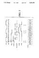
- a first embodiment of the present inventionin which there is provided a system 50, comprising a first logic circuit 52 which operates at a first clock speed CK A in a first timing domain, A, and a second logic circuit 70 which operates at a second clock speed CK B in a second timing domain, B.
- the first logic circuitincludes a transaction machine 54 which is capable of generating transaction requests to be transmitted to the second logic circuit 70 over a communication link 60.
- the communication linkmay include address lines, read/write lines, and data lines (61), together with a request line 62 and an acknowledge line 64.
- the first clock speedis slower than the second clock speed, and there is a predetermined frequency ratio between CK A and CK B . In a preferred embodiment, the first clock speed is at least three times slower than the second clock speed.
- the second logic circuit 70comprises a transaction machine 72 which is coupled to receive transaction information from the first logic circuit 54 over the communication link 60 including a transaction request on line 62 via synchronizing edge-triggered flip-flop 76. Transaction machine 72 is also coupled to return an acknowledge signal to the first logic circuit 52 over the acknowledge line 64 via a phase synchronization machine 74, which is shown to include a means for using input signals 77, following processing of the transaction. It is a particular feature of this embodiment that the duration of this transaction is of unknown length, but is typically less than a few tens of clock cycles.
- the phase synchronization machine 74is also coupled to receive the request signal REQ A from the first logic circuit via flip-flop 76, and to use that request signal to infer, with a constrained degree of ambiguity, the phase relationship between timing domain A and timing domain B at the time that phase synchronization circuit receives the signal.
- the systemoperates as follows.
- the transaction machine 54generates a transaction on communication link 60, including assertion of a transaction request pulse REQ A on line 62.
- Synchronizing flip-flop 76will pass this request B -- REQ A to both transaction machine 72 and phase synchronization machine 74 at the next rising edge of clock B (CK B ) at time t 1 .
- Phase synchronization machine 74then commences counting the clock cycles in timing domain B while transaction machine 72 implements the transaction.
- the phase synchronization machineis operative to count the number of clock cycles in timing domain B that elapse whilst the transaction is being processed, and to determine whether each of the clock edges associated with the clock cycles (CK B-- VALID?) may be regarded as legal, or illegal in timing domain A.
- a legal clock edgeis one where a signal transitioning on this edge will meet the set up and hold requirements of a flip-flop clocked in timing domain A.
- phase synchronization machinecauses a returning DONE signal from transaction machine 72, generated at time t 2 , to be propagated through to the ACK B output at time t 3 , and of sufficient duration that it will be sampled by clock A at time t 4 .
- ACK Bwill therefore not be propagated through to timing domain A over line 64 except to be synchronous to a legal clock edge of transaction machine 54.
- the state transitions of phase synchronization machine 74are indicated on the timing diagram as "STATE".
- phase synchronization machine 74While there is no REQ A asserted (!REQ A ), the phase synchronization machine remains in an idle state 200. Upon receipt of a request signal REQ A (and not a done signal (&!DONE)) the phase synchronization machine 74 transitions out of the idle state 200 and into the first of a number of states 205, 210, 225 indicating clock transitions legal in timing domain A. From any of these legal states, a DONE status in transaction machine 72 allows transition into the DONE state 230 of the phase synchronization machine, causing acknowledge signal ACK B to be transmitted to transaction machine 54.
- REQ Aand not a done signal (&!DONE)
- the DONE statemay not be entered, and the DONE signal from transaction machine 72 will not initiate the ACK B signal until the next legal state is entered.
- the loop 205-225will be more complex, and may involve a longer series of legal and illegal states within the loop.
- Multiple DONE states 230, 235, 240may be necessary to ensure that the ACK B signal is asserted for a long enough duration to be seen by one, and only one clock transition in timing domain A.
- the algorithm required to determine which clock edges in timing domain B may be usedis simple. Where the frequency ratio of the two timing domains is not a whole number, a more complex algorithm will be required.
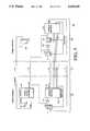
- a system 100comprising a first logic circuit 102 which operates at a first clock speed CK A in a first timing domain, A, and a second logic circuit 120 which operates at a second clock speed CK B in a second timing domain, B.
- the first logic circuitincludes a transaction machine 104 which is capable of generating transaction requests to be transmitted to a second logic circuit 120 over a communication link 110.
- the communication linkmay include address lines, read/write lines, and data lines (111), together with a request line 105, an "ALLOW" request line 112 and an acknowledge line 114. Additionally, there is a synchronization line 116.
- the first clock speed CK Ais faster than the second clock speed CK B .
- the first clock speedis at least three times faster than the second clock speed.
- the second logic circuit 120includes a transaction machine 122 which is coupled to receive transaction information from the first logic circuit 102 over the communication link 110, including a transaction request REQ A on line 105 via an edge detecting flip-flop 107, OR gate 109 and latch 119.
- Transaction machine 122is also coupled to return an acknowledge signal ACK to the first logic circuit 102 over the acknowledge line 114, via edge detecting flip-flop 126 and via AND gate 127, following processing of the transaction.
- Gating logic 109, 119, 127is controlled by the ALLOW signal provided on line 112 by the phase synchronization machine 106.
- the second logic circuit 120also includes a flip-flop 124 generating a clock change signal (B -- CHANGE) which indicates each transition of CK B : in effect, a signal with exactly one-half the frequency of CK B .
- the B -- CHANGE signalis transmitted to the first logic circuit 102 over synchronization line 116.
- a flip-flop 108is operative to pass this B -- CHANGE signal into timing domain A, where it is received by phase synchronization machine 106.
- the flip-flop 108provides the first rank of dual rank synchronization.
- the second rank of the dual rank synchronizationis provided by the state flip-flops which form part of the implementation of the phase synchronization machine 106.
- Phase synchronization machine 106is then operative to determine which clock edges in timing domain A will be valid in timing domain B, and to provide an indication of this to transaction machines 104, 122 on ALLOW line 112.
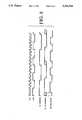
- the timing operationis as follows.
- the B -- CHANGE signalis asserted on line 116 by flip-flop 124, and is synchronized to timing domain A by edge-triggered flip-flop 108, which passes the signal to the S1 -- B -- CHANGE input of phase synchronization machine 106, synchronized with the next CK A rising clock edge.
- edge-triggered flip-flop 108which passes the signal to the S1 -- B -- CHANGE input of phase synchronization machine 106, synchronized with the next CK A rising clock edge.
- there is uncertainty which clock edge will cause this transitionshown as the two successive edges to the S1 -- B -- CHANGE signal.
- the transitionmay occur at time t 1 or at t 1 '. The same situation occurs with each transition in B -- CHANGE.
- phase synchronization machine 106By analysis of the situation for any fixed frequency relationship between clock A and clock B it is possible to determine the states required in phase synchronization machine 106 to track the transitions of S1 -- B -- CHANGE.
- the aimis to synthesize the ALLOW signal, which is shown in the diagram in its idealized form, such that the signal is never asserted during a B -- CHANGE transition for that particular frequency relationship.
- the phase synchronization machineis thus designed to accommodate the particular frequency ratio of the two circuits, and synthesizes the required ALLOW signal to accommodate the uncertainty of the time of transition of S1 -- B -- CHANGE at either t 1 or t 1 '.
- the precise sequence of states which will be followedwill depend upon the actual transition of S1 -- B -- CHANGE which takes place.
- the ideal ALLOW signalcannot be realized due to the ambiguity in the edges of S1 -- B -- CHANGE.
- a requestis generated by transaction machine 104 on communication link 110, including a transaction request pulse REQ A on line 105. This request is held on the output of edge detector 107. If signal ALLOW is asserted, then the output of edge detector 107 asserts: this indicates that CK B has not just changed, and is not about to change. In this situation, the request on the output of edge detector 107 is passed through OR gate 109 and latch 119. Once ALLOW negates, the request will be held on the output of latch 119, and will be sampled by the transaction machine 122 with no possibility of metastability.
- edge detector 107 and latch 119are reset by the transaction machine 122 upon receipt of the request using line "SEEN REQ".
- acknowledge signal ACK Bis passed from transaction machine 122 back to transaction machine 104 on line 114 via edge-detecting flip-flop 126.
- the ACK signalis held on the output of the edge detector 126. ALLOW will always be negated when the ACK signal is generated ensuring that a signal generated from a rising edge of CK B cannot immediately propagate into logic clocked by CK A .
- AND gate 127allows the output of edge detector 126 to propagate into transaction machine 104.
- Edge detector 126is reset by transaction machine 104 upon receipt of the ACK signal using line "SEEN ACK".
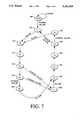
- FIG. 7there is shown a state diagram indicating the state transitions passed through by the phase synchronization machine 106 in the embodiment for which FIG. 6 represents the timing diagram (frequency ratio CK A :CK B is 5:1).
- the phase synchronization machineloops in an idle state 300 until S1 -- B -- CHANGE signal changes state (CHANGE).
- the phase synchronization machinetransitions into successive high states (H1 . . . Hn) until S1 -- B -- CHANGE transitions again (!CHANGE).
- the ALLOW signalis asserted (/ALLOW)
- the ALLOW signalWhen transitioning out of the H2 state, the ALLOW signal must be deasserted, since in the event that state H1 was entered at time t 1 ', and allowing for set-up and hold requirements, it is not safe to assert a request until after the next CHANGE signal.
- This CHANGE signalwill cause the phase synchronization machine to transition out of the H4, H5 or H6 states (320-330) to states L1, L1 or L2 respectively (335,340).
- the ALLOW signalmay once again be asserted after this transition, for a maximum of two clock cycles (CK A ), except that if state H6 has been entered, it is only safe to assert ALLOW for a single clock cycle thereafter.
- CK Aclock cycles
- the return path of the state diagram L3 to L6 (345-360)is similar, although note that the transition L4 to H1 is not required.
- the synthesized ALLOW signalcan only be asserted in states which fall into category 1. The result is that the signal ALLOW is asserted for a lower proportion of the time than the ideal allow signal ALLOW -- IDEAL.
- the frequency ratio between the two timing domainsis not a whole number, a different state diagram will be required, and the ALLOW signal will have a period which may vary from cycle to cycle, as shown in FIG. 8.
- the clock ratiois 4.5:1 (CK A :CK B ), and the uncertainty in the transition of S1 -- B -- CHANGE is shown at each rising edge only. It is known that the next transition in CK B will occur half way through a clock cycle CK A .
Landscapes
- Engineering & Computer Science (AREA)
- Theoretical Computer Science (AREA)
- Computer Networks & Wireless Communication (AREA)
- Signal Processing (AREA)
- Physics & Mathematics (AREA)
- General Engineering & Computer Science (AREA)
- General Physics & Mathematics (AREA)
- Information Transfer Systems (AREA)
Abstract
Description
Claims (10)
Applications Claiming Priority (2)
| Application Number | Priority Date | Filing Date | Title |
|---|---|---|---|
| GB9126513 | 1991-12-13 | ||
| GB9126513AGB2262415B (en) | 1991-12-13 | 1991-12-13 | Handshake synchronization system |
Publications (1)
| Publication Number | Publication Date |
|---|---|
| US5291529Atrue US5291529A (en) | 1994-03-01 |
Family
ID=10706223
Family Applications (1)
| Application Number | Title | Priority Date | Filing Date |
|---|---|---|---|
| US07/988,559Expired - LifetimeUS5291529A (en) | 1991-12-13 | 1992-12-10 | Handshake synchronization system |
Country Status (2)
| Country | Link |
|---|---|
| US (1) | US5291529A (en) |
| GB (1) | GB2262415B (en) |
Cited By (14)
| Publication number | Priority date | Publication date | Assignee | Title |
|---|---|---|---|---|
| US5420865A (en)* | 1994-06-08 | 1995-05-30 | Alcatel Data Networks | Method and apparatus for alignment of frames of information |
| US5487092A (en)* | 1994-12-22 | 1996-01-23 | International Business Machines Corporation | System for high-speed synchronization across clock domains |
| US5602878A (en)* | 1994-09-23 | 1997-02-11 | Intel Corporation | Method of delivering stable data across an asynchronous interface |
| US5684982A (en)* | 1994-09-07 | 1997-11-04 | Adaptec, Inc. | Synchronization circuit for clocked signals of similar frequencies |
| US5774704A (en)* | 1996-07-29 | 1998-06-30 | Silicon Graphics, Inc. | Apparatus and method for dynamic central processing unit clock adjustment |
| WO1999009654A3 (en)* | 1997-08-20 | 1999-06-03 | Nokia Telecommunications Oy | Method for performing phase comparison, and phase comparator |
| FR2775088A1 (en)* | 1998-02-19 | 1999-08-20 | Sgs Thomson Microelectronics | Integrated circuit with master and slave circuits operating at a first and second frequency respectively |
| US6097775A (en)* | 1998-02-17 | 2000-08-01 | Lsi Logic Corporation | Method and apparatus for synchronously transferring signals between clock domains |
| US6112016A (en)* | 1995-04-12 | 2000-08-29 | Intel Corporation | Method and apparatus for sharing a signal line between agents |
| US20020150189A1 (en)* | 1997-10-10 | 2002-10-17 | Rambus Incorporated | Apparatus and method for generating a distributed clock signal using gear ratio techniques |
| WO2002031664A3 (en)* | 2000-10-12 | 2003-05-01 | Celoxica Ltd | System, method and article of manufacture for data transfer across clock domains |
| WO2005002129A1 (en) | 2003-06-25 | 2005-01-06 | Koninklijke Philips Electronics, N.V. | Lossless transfer of events across clock domains |
| US20060053348A1 (en)* | 2004-09-09 | 2006-03-09 | International Business Machines Corporation | Dynamic frequency scaling sequence for multi-gigahertz microprocessors |
| US20110221498A1 (en)* | 2010-03-15 | 2011-09-15 | Stmicroelectronics S.R.L. | System for synchronizing operation of a circuit with a control signal, and corresponding integrated circuit |
Families Citing this family (4)
| Publication number | Priority date | Publication date | Assignee | Title |
|---|---|---|---|---|
| US5687358A (en)* | 1994-08-02 | 1997-11-11 | Melco, Inc. | Accelerator for mounting and interfacing a second CPU onto a motherboard |
| DE69430058T2 (en)* | 1994-08-05 | 2002-11-28 | Melco Inc., Nagoya | accelerator |
| US5634116A (en)* | 1995-03-30 | 1997-05-27 | International Business Machines Corporation | Non-integer multiple clock translator |
| SE521447C2 (en)* | 1999-06-08 | 2003-11-04 | Ericsson Telefon Ab L M | Method and arrangements to prevent metastability |
Citations (9)
| Publication number | Priority date | Publication date | Assignee | Title |
|---|---|---|---|---|
| US4017740A (en)* | 1975-04-30 | 1977-04-12 | Hewlett-Packard Company | Synchronization of digital circuits by bus triggering |
| US4070630A (en)* | 1976-05-03 | 1978-01-24 | Motorola Inc. | Data transfer synchronizing circuit |
| US4289976A (en)* | 1978-11-10 | 1981-09-15 | Robert Bosch Gmbh | Circuit arrangement for the transmission of digital data |
| US4727370A (en)* | 1985-12-17 | 1988-02-23 | Ampex Corporation | Method and system for synchronous handshake generation |
| US4873703A (en)* | 1985-09-27 | 1989-10-10 | Hewlett-Packard Company | Synchronizing system |
| US4973860A (en)* | 1989-05-02 | 1990-11-27 | Ast Research Inc. | Circuit for synchronizing an asynchronous input signal to a high frequency clock |
| US5012138A (en)* | 1988-07-26 | 1991-04-30 | Yamaha Corporation | Interface circuit for asychronous data transfer |
| US5036221A (en)* | 1989-03-31 | 1991-07-30 | Texas Instruments Incorporated | Circuit for eliminating metastable events associated with a data signal asynchronous to a clock signal |
| US5045801A (en)* | 1990-05-29 | 1991-09-03 | The United States Of America As Represented By The Secretary Of The Air Force | Metastable tolerant asynchronous interface |
- 1991
- 1991-12-13GBGB9126513Apatent/GB2262415B/ennot_activeExpired - Fee Related
- 1992
- 1992-12-10USUS07/988,559patent/US5291529A/ennot_activeExpired - Lifetime
Patent Citations (9)
| Publication number | Priority date | Publication date | Assignee | Title |
|---|---|---|---|---|
| US4017740A (en)* | 1975-04-30 | 1977-04-12 | Hewlett-Packard Company | Synchronization of digital circuits by bus triggering |
| US4070630A (en)* | 1976-05-03 | 1978-01-24 | Motorola Inc. | Data transfer synchronizing circuit |
| US4289976A (en)* | 1978-11-10 | 1981-09-15 | Robert Bosch Gmbh | Circuit arrangement for the transmission of digital data |
| US4873703A (en)* | 1985-09-27 | 1989-10-10 | Hewlett-Packard Company | Synchronizing system |
| US4727370A (en)* | 1985-12-17 | 1988-02-23 | Ampex Corporation | Method and system for synchronous handshake generation |
| US5012138A (en)* | 1988-07-26 | 1991-04-30 | Yamaha Corporation | Interface circuit for asychronous data transfer |
| US5036221A (en)* | 1989-03-31 | 1991-07-30 | Texas Instruments Incorporated | Circuit for eliminating metastable events associated with a data signal asynchronous to a clock signal |
| US4973860A (en)* | 1989-05-02 | 1990-11-27 | Ast Research Inc. | Circuit for synchronizing an asynchronous input signal to a high frequency clock |
| US5045801A (en)* | 1990-05-29 | 1991-09-03 | The United States Of America As Represented By The Secretary Of The Air Force | Metastable tolerant asynchronous interface |
Cited By (28)
| Publication number | Priority date | Publication date | Assignee | Title |
|---|---|---|---|---|
| US5420865A (en)* | 1994-06-08 | 1995-05-30 | Alcatel Data Networks | Method and apparatus for alignment of frames of information |
| US5684982A (en)* | 1994-09-07 | 1997-11-04 | Adaptec, Inc. | Synchronization circuit for clocked signals of similar frequencies |
| US5729719A (en)* | 1994-09-07 | 1998-03-17 | Adaptec, Inc. | Synchronization circuit for clocked signals of similar frequencies |
| US5602878A (en)* | 1994-09-23 | 1997-02-11 | Intel Corporation | Method of delivering stable data across an asynchronous interface |
| US5487092A (en)* | 1994-12-22 | 1996-01-23 | International Business Machines Corporation | System for high-speed synchronization across clock domains |
| US6112016A (en)* | 1995-04-12 | 2000-08-29 | Intel Corporation | Method and apparatus for sharing a signal line between agents |
| US5774704A (en)* | 1996-07-29 | 1998-06-30 | Silicon Graphics, Inc. | Apparatus and method for dynamic central processing unit clock adjustment |
| AU745305B2 (en)* | 1997-08-20 | 2002-03-21 | Nokia Telecommunications Oy | Method for performing phase comparison, and phase comparator |
| WO1999009654A3 (en)* | 1997-08-20 | 1999-06-03 | Nokia Telecommunications Oy | Method for performing phase comparison, and phase comparator |
| US6532257B1 (en) | 1997-08-20 | 2003-03-11 | Nokia Telecommunications Oy | Method for performing phase comparison, and phase comparator |
| US20020150189A1 (en)* | 1997-10-10 | 2002-10-17 | Rambus Incorporated | Apparatus and method for generating a distributed clock signal using gear ratio techniques |
| US20050063502A1 (en)* | 1997-10-10 | 2005-03-24 | Rambus, Inc. | Apparatus and method for generating a distributed clock signal |
| US6836521B2 (en)* | 1997-10-10 | 2004-12-28 | Rambus Inc. | Apparatus and method for generating a distributed clock signal using gear ratio techniques |
| US7263149B2 (en) | 1997-10-10 | 2007-08-28 | Rambus Inc. | Apparatus and method for generating a distributed clock signal |
| US6097775A (en)* | 1998-02-17 | 2000-08-01 | Lsi Logic Corporation | Method and apparatus for synchronously transferring signals between clock domains |
| US6175257B1 (en)* | 1998-02-19 | 2001-01-16 | Stmicroelectronics S.A. | Integrated circuit comprising a master circuit working at a first frequency to control slave circuits working at a second frequency |
| FR2775088A1 (en)* | 1998-02-19 | 1999-08-20 | Sgs Thomson Microelectronics | Integrated circuit with master and slave circuits operating at a first and second frequency respectively |
| WO2002031664A3 (en)* | 2000-10-12 | 2003-05-01 | Celoxica Ltd | System, method and article of manufacture for data transfer across clock domains |
| WO2005002129A1 (en) | 2003-06-25 | 2005-01-06 | Koninklijke Philips Electronics, N.V. | Lossless transfer of events across clock domains |
| US20110096880A1 (en)* | 2003-06-25 | 2011-04-28 | Nxp, B.V. | Lossless Transfer Of Events Across Clock Domains |
| EP1676391B1 (en)* | 2003-06-25 | 2011-05-18 | Nxp B.V. | Lossless transfer of events across clock domains |
| US8284879B2 (en) | 2003-06-25 | 2012-10-09 | Nxp B.V. | Lossless transfer of events across clock domains |
| US20060053348A1 (en)* | 2004-09-09 | 2006-03-09 | International Business Machines Corporation | Dynamic frequency scaling sequence for multi-gigahertz microprocessors |
| US7516350B2 (en)* | 2004-09-09 | 2009-04-07 | International Business Machines Corporation | Dynamic frequency scaling sequence for multi-gigahertz microprocessors |
| US20090119552A1 (en)* | 2004-09-09 | 2009-05-07 | Nathan Chelstrom | Dynamic Frequency Scaling Sequence for Multi-Gigahertz Microprocessors |
| US7702944B2 (en) | 2004-09-09 | 2010-04-20 | International Business Machines Corporation | Dynamic frequency scaling sequence for multi-gigahertz microprocessors |
| US20110221498A1 (en)* | 2010-03-15 | 2011-09-15 | Stmicroelectronics S.R.L. | System for synchronizing operation of a circuit with a control signal, and corresponding integrated circuit |
| US8390346B2 (en)* | 2010-03-15 | 2013-03-05 | Stmicroelectronics, Srl | System for synchronizing operation of a circuit with a control signal, and corresponding integrated circuit |
Also Published As
| Publication number | Publication date |
|---|---|
| GB2262415A (en) | 1993-06-16 |
| GB2262415B (en) | 1995-08-16 |
| GB9126513D0 (en) | 1992-02-12 |
Similar Documents
| Publication | Publication Date | Title |
|---|---|---|
| US5291529A (en) | Handshake synchronization system | |
| KR101089153B1 (en) | Integrated circuits and methods of transmitting data signals between different clock domains | |
| EP0666541B1 (en) | Apparatus and method for operating chips synchronously at speeds exceeding the bus speed | |
| JP3517237B2 (en) | Synchronous bus system and memory device therefor | |
| US5602878A (en) | Method of delivering stable data across an asynchronous interface | |
| US4390969A (en) | Asynchronous data transmission system with state variable memory and handshaking protocol circuits | |
| EP0352081B1 (en) | Efficient protocol for communicating between asynchronous devices | |
| CA2365288C (en) | Dynamic wave-pipelined interface apparatus and methods therefor | |
| JPH03157030A (en) | data processing equipment | |
| US7500131B2 (en) | Training pattern based de-skew mechanism and frame alignment | |
| US7134035B2 (en) | Method for generating a synchronization signal based on the clock ratio between two clock domains for data transfer between the domains | |
| JP2928866B2 (en) | Programmable data transfer timing | |
| US5923193A (en) | Method and apparatus for transferring signals between multiple clock timing domains | |
| US6172540B1 (en) | Apparatus for fast logic transfer of data across asynchronous clock domains | |
| US5706485A (en) | Method and apparatus for synchronizing clock signals in a multiple die circuit including a stop clock feature | |
| US6087867A (en) | Transaction control circuit for synchronizing transactions across asynchronous clock domains | |
| US6928574B1 (en) | System and method for transferring data from a lower frequency clock domain to a higher frequency clock domain | |
| US6067629A (en) | Apparatus and method for pseudo-synchronous communication between clocks of different frequencies | |
| US6760392B1 (en) | Method and apparatus to provide fixed latency early response in a system with multiple clock domains with fixable clock ratios | |
| US6931562B1 (en) | System and method for transferring data from a higher frequency clock domain to a lower frequency clock domain | |
| US7248661B1 (en) | Data transfer between phase independent clock domains | |
| JP3604637B2 (en) | Asynchronous transfer device and asynchronous transfer method | |
| US6651127B2 (en) | Method of detecting termination of a bus transfer operation | |
| JPH01288128A (en) | Two-way data transfer control method | |
| Del Corso et al. | Resynchronization Interfaces: Sources of Metastability Errors in Computing Systems |
Legal Events
| Date | Code | Title | Description |
|---|---|---|---|
| AS | Assignment | Owner name:DIGITAL EQUIPMENT CORPORATION, MASSACHUSETTS Free format text:ASSIGNMENT OF ASSIGNORS INTEREST.;ASSIGNORS:CROOK, NEAL ANDREW;BRUCE, PAUL LESTER;GALUSZKA, ROBERT JEFFREY;REEL/FRAME:006458/0001 Effective date:19921209 | |
| AS | Assignment | Owner name:DIGITAL EQUIPMENT INTERNATIONAL LIMITED, SWITZERLA Free format text:ASSIGNMENT OF ASSIGNORS INTEREST.;ASSIGNORS:CROOK, NEAL ANDREW;BRUCE, PAUL LESTER;GALUSZKA, ROBERT JEFFREY;REEL/FRAME:006458/0059 Effective date:19930208 | |
| STCF | Information on status: patent grant | Free format text:PATENTED CASE | |
| FPAY | Fee payment | Year of fee payment:4 | |
| AS | Assignment | Owner name:CABLETRON SYSTEMS, INC., NEW HAMPSHIRE Free format text:ASSIGNMENT OF ASSIGNORS INTEREST;ASSIGNOR:DIGITAL EQUIPMENT CORPORATION;REEL/FRAME:009187/0912 Effective date:19980206 | |
| FEPP | Fee payment procedure | Free format text:PAYOR NUMBER ASSIGNED (ORIGINAL EVENT CODE: ASPN); ENTITY STATUS OF PATENT OWNER: LARGE ENTITY | |
| AS | Assignment | Owner name:ENTERASYS NETWORKS, INC., NEW HAMPSHIRE Free format text:ASSIGNMENT OF ASSIGNORS INTEREST;ASSIGNOR:CABLETRON SYSTEMS, INC.;REEL/FRAME:011219/0376 Effective date:20000929 | |
| FPAY | Fee payment | Year of fee payment:8 | |
| FPAY | Fee payment | Year of fee payment:12 | |
| AS | Assignment | Owner name:OBSIDIAN, LLC, CALIFORNIA Free format text:SECURITY AGREEMENT;ASSIGNOR:ENTERASYS NETWORKS, INC.;REEL/FRAME:017656/0552 Effective date:20060516 Owner name:WELLS FARGO FOOTHILL, INC., CALIFORNIA Free format text:SECURITY AGREEMENT;ASSIGNOR:ENTERASYS NETWORKS, INC.;REEL/FRAME:017656/0552 Effective date:20060516 | |
| AS | Assignment | Owner name:WELLS FARGO TRUST CORPORATION LIMITED, AS SECURITY Free format text:GRANT OF SECURITY INTEREST IN U.S. PATENTS;ASSIGNOR:ENTERASYS NETWORKS INC.;REEL/FRAME:025339/0875 Effective date:20101109 | |
| AS | Assignment | Owner name:ENTERASYS NETWORKS, INC., MASSACHUSETTS Free format text:RELEASE AND REASSIGNMENT OF PATENTS AND PATENT APPLICATIONS AT REEL/FRAME NO. 17656/0552;ASSIGNORS:WELLS FARGO CAPITAL FINANCE, INC. (FORMERLY KNOWN AS WELLS FARGO FOOTHILL, INC.);ENTERPRISE COMMUNICATIONS FUNDING GMBH, AS SUCCESSOR IN INTEREST TO OBSIDIAN, LLC;REEL/FRAME:025406/0769 Effective date:20101110 |