US5290382A - Methods and apparatus for generating a plasma for "downstream" rapid shaping of surfaces of substrates and films - Google Patents
Methods and apparatus for generating a plasma for "downstream" rapid shaping of surfaces of substrates and filmsDownload PDFInfo
- Publication number
- US5290382A US5290382AUS07/807,536US80753691AUS5290382AUS 5290382 AUS5290382 AUS 5290382AUS 80753691 AUS80753691 AUS 80753691AUS 5290382 AUS5290382 AUS 5290382A
- Authority
- US
- United States
- Prior art keywords
- plasma
- substrate
- chamber
- plasma chamber
- outlet
- Prior art date
- Legal status (The legal status is an assumption and is not a legal conclusion. Google has not performed a legal analysis and makes no representation as to the accuracy of the status listed.)
- Expired - Fee Related
Links
Images

Classifications
- H—ELECTRICITY
- H01—ELECTRIC ELEMENTS
- H01J—ELECTRIC DISCHARGE TUBES OR DISCHARGE LAMPS
- H01J37/00—Discharge tubes with provision for introducing objects or material to be exposed to the discharge, e.g. for the purpose of examination or processing thereof
- H01J37/32—Gas-filled discharge tubes
- H01J37/32431—Constructional details of the reactor
- H01J37/32623—Mechanical discharge control means
- H—ELECTRICITY
- H01—ELECTRIC ELEMENTS
- H01L—SEMICONDUCTOR DEVICES NOT COVERED BY CLASS H10
- H01L21/00—Processes or apparatus adapted for the manufacture or treatment of semiconductor or solid state devices or of parts thereof
- H01L21/02—Manufacture or treatment of semiconductor devices or of parts thereof
- H01L21/04—Manufacture or treatment of semiconductor devices or of parts thereof the devices having potential barriers, e.g. a PN junction, depletion layer or carrier concentration layer
- H01L21/18—Manufacture or treatment of semiconductor devices or of parts thereof the devices having potential barriers, e.g. a PN junction, depletion layer or carrier concentration layer the devices having semiconductor bodies comprising elements of Group IV of the Periodic Table or AIIIBV compounds with or without impurities, e.g. doping materials
- H01L21/30—Treatment of semiconductor bodies using processes or apparatus not provided for in groups H01L21/20 - H01L21/26
- H01L21/302—Treatment of semiconductor bodies using processes or apparatus not provided for in groups H01L21/20 - H01L21/26 to change their surface-physical characteristics or shape, e.g. etching, polishing, cutting
- H01L21/304—Mechanical treatment, e.g. grinding, polishing, cutting
- H—ELECTRICITY
- H01—ELECTRIC ELEMENTS
- H01J—ELECTRIC DISCHARGE TUBES OR DISCHARGE LAMPS
- H01J37/00—Discharge tubes with provision for introducing objects or material to be exposed to the discharge, e.g. for the purpose of examination or processing thereof
- H01J37/32—Gas-filled discharge tubes
- H01J37/32009—Arrangements for generation of plasma specially adapted for examination or treatment of objects, e.g. plasma sources
- H01J37/32357—Generation remote from the workpiece, e.g. down-stream
- H—ELECTRICITY
- H01—ELECTRIC ELEMENTS
- H01J—ELECTRIC DISCHARGE TUBES OR DISCHARGE LAMPS
- H01J37/00—Discharge tubes with provision for introducing objects or material to be exposed to the discharge, e.g. for the purpose of examination or processing thereof
- H01J37/32—Gas-filled discharge tubes
- H01J37/32009—Arrangements for generation of plasma specially adapted for examination or treatment of objects, e.g. plasma sources
- H01J37/32366—Localised processing
- H—ELECTRICITY
- H01—ELECTRIC ELEMENTS
- H01J—ELECTRIC DISCHARGE TUBES OR DISCHARGE LAMPS
- H01J37/00—Discharge tubes with provision for introducing objects or material to be exposed to the discharge, e.g. for the purpose of examination or processing thereof
- H01J37/32—Gas-filled discharge tubes
- H01J37/32431—Constructional details of the reactor
- H01J37/32623—Mechanical discharge control means
- H01J37/32633—Baffles
Definitions
- the present inventionrelates to a method and apparatus for controlled material removal from the surface of a substrate over a confined region, and more particularly, to a method and apparatus for removing material from the surface of a substrate by a reactive and excited species created in a plasma generated so that the substrate is independent of the means for generating the plasma.
- the present inventionprovides a means for accomplishing controlled, localized material removal for error correction in precision figuring of optical surfaces and thickness profile controlling of films of semiconductor devices while avoiding the effects of substrate geometry on the removal process and a reducing the potential contamination of the surface of the substrate.
- chemomechanical processes for thinning semiconductor filmsis a contact method that leaves contaminants on the surface which cause subsurface damage to the substrate.
- chemomechanical thinning processesdo not allow corrections of the spatial variations within the film thickness.
- Plasma assisted chemical etching methods to shape surfaces of substratesare an improvement over the prior art processes such as chemomechanical thinning because such plasma processes do not contact the substrate surface, and, therefore, reduce the potential for subsurface damage.
- U.S. Pat. No. 4,668,336discloses a method and apparatus for figuring a surface by plasma assisted chemical transport where the substrate surface is mounted in close proximity to at least one electrode of an rf driven reactor having two parallel plate electrodes. Removal of material from the surface of a substrate is controlled by varying the amount of time an electrode with small surface area spends at a given region wherein the entire surface of the substrate is subjected to the presence of reactive gas which in the presence of an rf field between the two electrodes forms a plasma. Thus, material removal is effected by a plasma which is generated at the surface where material removal is desired.
- a disadvantage to the invention disclosed thereinis that the profile of the surface where the material has been removed may not be precisely controlled.
- the device disclosed thereinis of the type where the plasma excitation occurs by rf discharge directly coupled to the substrate (the local substrate surface is effectively an electrode where the reaction is occurring), underlying surface structure may cause variations in the material removal rate which is a primary cause of "print through" problems.
- the downstream methodproduces a dry chemical removal process over the substrate which eliminates damage to the substrate which could result from energetic species.
- the method disclosed thereinfails to provide a means to make precise changes to the profile of the surface where material is removed and, therefore, is not useful for local error correction of a substrate surface.
- the present inventionincorporates the advantages of decoupled plasma assisted chemical etching with a means to perform local etching so as to correct spatial errors in the substrate surface or correct the thickness profile of a film on a substrate.
- the present inventionis directed to a method and apparatus for local plasma assisted chemical etching wherein the plasma is generated away and independent (decoupled) from a substrate etching surface.
- the process of decoupling plasma generation from the etching reaction siteavoids many of the problems associated with substrate geometry when the plasma is generated locally and coupled to the site.
- the advantage of decoupled plasma generationis that it avoids uncontrolled removal rate variations caused by subsurface structure when the plasma is generated locally.
- the present inventionprovides a means to control local material removal rates.
- the present inventiongenerally comprises a plasma chamber having a gas inlet, and an outlet for flowing a chemically reactive and neutral species created by a plasma "downstream" to a reaction site on the surface of a substrate.
- the independently generated plasmais generated in a region which is located a distance away from the substrate surface that is to be etched.
- the plasma and its chemically reactive and neutral speciesmay be generated "upstream” by a radio frequency (rf) power source directly coupled to the plasma and gas mixture as in a parallel plate rf discharge, inductively coupled to the plasma and gas mixture as in a toroidal coil rf discharge, or capacitively coupled to the plasma and gas mixture as in a solenoid coil driven at high frequencies.
- the plasma and reactive speciesmay also be generated "upstream” by microwave excitation techniques.
- the plasma generated by any of the above meansflows "downstream" to the reaction site through an outlet which may have an interactive shaped skirt to prevent etching outside of a local material removal footprint.
- the footprintis defined by the size of the outlet, the distance from the substrate, the gas flow, and the plasma parameters.
- Material removal on the surface of the substrateis performed locally by chemically reactive species created by the "upstream” plasma.
- the chemical reaction rate at the surfacemay be enhanced by a flux of non-thermal energy carried by the excited neutral species also created by the "upstream” plasma. Because the plasma generation is sufficiently far from the surface of the etching area, undesired and short-lived active species such as ions are temporally “filtered” out of the reactive plasma gas flow stream before reaching the etching surface. The remaining long-lived excited neutral and chemically reactive "radicals" are carried “downstream” through the outlet to the local etching surface by the gas flux. These long-lived species enhance the rate of chemical reaction at the surface by giving up their stored energy during the etching process.
- the shaped gas outlet of the present inventionprovides a means to prevent unwanted etching outside the localized material removal footprint by supplying a surface separate from the substrate to consume the reactive species.
- the present inventionprovides a useful and controllable means for correcting local surface errors in the optical figuring and film thinning processes that is non-damaging and non-contaminating to the surface of the substrate.
- One objective of the present inventionis to provide a means for performing a plasma assisted chemical etching reaction.
- Another objective of the present inventionis to provide a means for material removal by a chemically reactive species from a plasma generated independent of the electrical and geometric characteristics of the substrate.
- Another objective of the present inventionis to provide a means for local application of a decoupled plasma for precision optical figuring or film thinning.
- Another objective of the present inventionis to provide a means for preventing unwanted etching reactions outside of the local material removal footprint.
- FIG. 1is a schematic diagram of a plasma reactor with an integral interactive skirt at the outlet for controlling local material removal in the downstream mode.
- FIG. 2is a schematic diagram of a parallel plate rf discharge downstream plasma reactor system.
- FIG. 3is a schematic diagram of an inductively coupled downstream plasma reactor system.
- FIG. 4is a schematic diagram of an rf discharge downstream plasma reactor system driven by a solenoid coil.
- the plasma assisted chemical etching method of the present invention for figuring optical surfaces and thinning films on substratesis generally performed by passing active species (chemically reactive and excited species) generated in a plasma region on to a substrate surface to be etched.
- the active species createdare generated by excitation which is "upstream" and independent of the surface to be etched.
- the decoupled generation of the plasma and active species thereofprovide a means to prevent the occurrence of "print through” phenomena typically experienced when plasma is generated by an excitation means which incorporates the substrate therein.
- Decoupled plasma generationrequires the use of higher power densities to generate the active species because those species must travel to the etching site while still excited but not directly influenced by the means for excitation.
- the use of higher power densitiesin turn, can cause local etching of the region where the plasma is generated.
- the method of the present inventionincorporates the use of apparatus which can overcome these shortfalls, such as "print through” and local etching at plasma generation region.
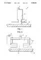
- the apparatus of the present inventionincludes a plasma assisted chemical etching reactor 10 for performing local "downstream" etching reactions of substrate surfaces which comprises a plasma chamber 12 having a gas inlet 14 at one end and a gas outlet 16 at the other end.
- the inlet 14is connected to a source of gas (not shown).
- the gas introduced into the plasma chamberis transformed into a plasma by the application of a source of excitation.
- the excitation sourcemay be radio frequency (rf) power or microwave energy.
- the "downstream" outlet 16comprises an orifice which is approximately dimensioned to the size of the removal footprint desired for local material removal.
- the outletmay have an associated skirt 18 attached to its terminal end which is fabricated out of a material which is interactive with active species responsible for "downstream" etching.
- Silicon and carbonare materials may be used as the interactive skirt.
- the skirt 18provides a surface to consume reactive species which is separate from the substrate surface. When used, the skirt is dimensioned and placed so that its surface is proximal to the surface of the substrate outside of the footprint area.
- the distance d between the terminal end of the outlet 16 and the surface of an etchable substrate 20can be varied by a reactor support means (not shown).
- the reactoralso has means (not shown) to vary the tilt of the reactor with respect to the substrate surface. Because the removal footprint profile varies with the distance between the outlet 16 and the surface of the substrate, these adjustment means allow variations in the removal footprint profile.
- the upstream plasma generation at the plasma chamber 12may be accomplished in a number of ways.
- the plasmamay be generated by rf excitation of the reactive gas coupled directly, capacitively, or inductively to an rf power source or it may be generated by microwave excitation.
- FIG. 2a directly coupled embodiment having two parallel plate electrodes directly coupled to the plasma and gas mixture is shown.
- an rf power source 22is applied to a pair of parallel plate electrodes 24 located at opposite ends of the plasma chamber 12.
- Gasis continuously fed into the chamber via the inlet 14 where it is converted to a plasma having long-lived active species for etching reactions.
- the active speciesare then applied to the surface through the outlet 16.
- an inductively coupled embodiment having a ferromagnetic toroidal coil located proximally to a toroidal shaped plasma chamberis illustrated.
- gasis fed into the plasma chamber 12a which has a general toroidal shape.
- the plasmais generated by applying the rf power source 22 to a ferromagnetic toroid 26 placed adjacent to the toroid shaped plasma chamber 12a containing the gas.
- the plasma within the chamber 12aacts as a secondary loop around the toroidal core 19.
- the plasma and reactive species thereofare flowed through the outlet 16 to the substrate.
- FIG. 4illustrates yet another embodiment wherein the generation of the active species is decoupled from the substrate.
- the gasis continuously fed through the inlet 14 and is broken down into a plasma by the application of rf power 22 to a solenoid coil 30 wrapped around the tubular plasma chamber 12b.
- this embodimentmay act in a capacitative or inductive manner.
- the resulting active speciesare flowed out through the outlet 16 to the substrate surface.
- the rf power frequency used to generate the plasmamay be anywhere from direct current to microwave (gigahertz). However, each of the above mentioned embodiments works best in certain frequency ranges. For example, direct coupling while in theory operational at all frequencies, is usually limited to frequencies less than one (1) MHz. Inductively coupled embodiments operate best above a frequency where the shunt inductive primary impedance is larger than that of the discharge (usually between 1 KHz and 1 MHz). Capacitive coupling embodiments are best suited to high frequencies (10 MHz to 1 GHz) depending on the geometry of the coupling system. A frequency of 13.5 13 MHz has been successfully used in an inductive coupling embodiment and is a frequency which is readily available.
- the generation of the plasma physically apart and away from the substrate surface in the decoupled embodiments of the present inventionyields the advantage of permitting short lived active species such as ions to be temporally filtered out and allowing the much longer lived active species to be carried downstream by the flow of gas so that upon arrival at the etching surface, they are allowed to give up their stored energy to enhance the rate of chemical reaction that permits etching.
- the advantage of decoupled plasma generationrequires higher power densities than those of coupled generation. The use of higher power densities results in etching of the local plasma region and higher risks of substrate surface contamination.
- Superior decoupled plasma generation embodiments for downstream active species generationare embodiments which permit the use of high power densities without forming energetic ion fluxes incident on the walls of the plasma chamber 12 that result in sputter removal and/or accelerated plasma assisted chemical etching of the plasma chamber walls.
- Inductive coupling embodimentsare preferred because the electric fields are parallel to the toroidal plasma chamber and the resulting energy of the ions striking the chamber walls is lower.
- inductive couplingmay not be practical because it is too difficult to generate and sustain a plasma.
- an important considerationis to select a wall material which has a low sputtering coefficient and a low chemical reactivity with the plasma excited gas. Such wall material considerations prevents contamination of the substrate surface being etched.
- Materials that may be etched by the present inventioninclude chromium, aluminum, silicon, silicon dioxide and various other photoresists.
- the present inventioncan achieve removal rates as high as 3 microns per minute for common optical and semiconductor materials, such as Si and SiO 2 .
- the material removal of optical and semiconductor materials Si and SiO 2can be accomplished with a number of gases when using any of the "downstream" mode embodiments of the present invention.
- High downstream removal rates(rates greater than 3 microns per minute) can be obtained when nitrogen trifluoride (NF 3 ) or a mixture of gases including NF 3 is fed into the plasma chamber.
- Gases such as NF 3can give rise to small, but unwanted etching outside the localized material removal footprint area. However, the etching can be confined by using the interactive skirt 18 over the substrate and around the localized etch area.
- Local etching of the substrate surfaceis accomplished by moving the outlet orifice 16 along the substrate surface in a manner which is determined by the area of material removal and footprint shape desired.
- the shape of the material removal footprint profilemay be changed by varying the distance d between the outlet orifice 16 with interactive skirt 18, and the surface of the substrate 20. By increasing d, a gaussian like profile may be achieved. By decreasing the distance d, a top hat-like profile may be achieved.
- the downstream removal apparatus of the present inventionat a relatively large distance (1 cm) from the substrate 20, the removal of material becomes insensitive to small changes in the distance d that can be caused by a small sag in an optical or other surface being figured.
- the apparatus of the present inventioncan provide a means for making accurate corrections of substrate errors without having additional means for programmed positional controls of the plasma generator for distance d and tilt with respect to the substrate.
- the present inventionprovides a means for making local error corrections useful for thinning semiconductor films and figuring optics while avoiding "print through" problems associated with particular substrate characteristics.
Landscapes
- Engineering & Computer Science (AREA)
- Physics & Mathematics (AREA)
- Plasma & Fusion (AREA)
- Chemical & Material Sciences (AREA)
- Analytical Chemistry (AREA)
- General Physics & Mathematics (AREA)
- Condensed Matter Physics & Semiconductors (AREA)
- Manufacturing & Machinery (AREA)
- Computer Hardware Design (AREA)
- Microelectronics & Electronic Packaging (AREA)
- Power Engineering (AREA)
- Drying Of Semiconductors (AREA)
- ing And Chemical Polishing (AREA)
- Plasma Technology (AREA)
Abstract
Description
Claims (8)
Priority Applications (6)
| Application Number | Priority Date | Filing Date | Title |
|---|---|---|---|
| US07/807,536US5290382A (en) | 1991-12-13 | 1991-12-13 | Methods and apparatus for generating a plasma for "downstream" rapid shaping of surfaces of substrates and films |
| EP92311336AEP0546852A1 (en) | 1991-12-13 | 1992-12-11 | Methods and apparatus for generating a plasma for "downstream" rapid shaping of surfaces of substrates and films |
| KR1019920024114AKR930014826A (en) | 1991-12-13 | 1992-12-12 | Method and apparatus for generating plasma to rapidly form the surface of substrates and films "downstream" |
| IL10409292AIL104092A (en) | 1991-12-13 | 1992-12-14 | Methods and apparatus for generating a plasma for "downstream" rapid shaping of surfaces of substrates and films |
| JP4353612AJPH05267233A (en) | 1991-12-13 | 1992-12-14 | Plasma generation method and apparatus for rapid shaping downstream of substrate and film surfaces |
| TW081110253ATW214615B (en) | 1991-12-13 | 1992-12-21 |
Applications Claiming Priority (1)
| Application Number | Priority Date | Filing Date | Title |
|---|---|---|---|
| US07/807,536US5290382A (en) | 1991-12-13 | 1991-12-13 | Methods and apparatus for generating a plasma for "downstream" rapid shaping of surfaces of substrates and films |
Publications (1)
| Publication Number | Publication Date |
|---|---|
| US5290382Atrue US5290382A (en) | 1994-03-01 |
Family
ID=25196605
Family Applications (1)
| Application Number | Title | Priority Date | Filing Date |
|---|---|---|---|
| US07/807,536Expired - Fee RelatedUS5290382A (en) | 1991-12-13 | 1991-12-13 | Methods and apparatus for generating a plasma for "downstream" rapid shaping of surfaces of substrates and films |
Country Status (6)
| Country | Link |
|---|---|
| US (1) | US5290382A (en) |
| EP (1) | EP0546852A1 (en) |
| JP (1) | JPH05267233A (en) |
| KR (1) | KR930014826A (en) |
| IL (1) | IL104092A (en) |
| TW (1) | TW214615B (en) |
Cited By (258)
| Publication number | Priority date | Publication date | Assignee | Title |
|---|---|---|---|---|
| US5375064A (en)* | 1993-12-02 | 1994-12-20 | Hughes Aircraft Company | Method and apparatus for moving a material removal tool with low tool accelerations |
| US5474642A (en)* | 1991-05-24 | 1995-12-12 | Overseas Publishers Association | Apparatus for the treatment of a solid body |
| US5766494A (en)* | 1994-08-29 | 1998-06-16 | Kabushiki Kaisha Toshiba | Etching method and apparatus |
| US5900104A (en)* | 1996-06-04 | 1999-05-04 | Boeing North American, Inc. | Plasma system for enhancing the surface of a material |
| DE19833257C1 (en)* | 1998-07-23 | 1999-09-30 | Wacker Siltronic Halbleitermat | Semiconductor wafer production process especially to produce a silicon wafer for fabricating sub-micron line width electronic devices |
| US5998933A (en)* | 1998-04-06 | 1999-12-07 | Shun'ko; Evgeny V. | RF plasma inductor with closed ferrite core |
| US6030887A (en)* | 1998-02-26 | 2000-02-29 | Memc Electronic Materials, Inc. | Flattening process for epitaxial semiconductor wafers |
| US6074947A (en)* | 1998-07-10 | 2000-06-13 | Plasma Sil, Llc | Process for improving uniform thickness of semiconductor substrates using plasma assisted chemical etching |
| US6150628A (en)* | 1997-06-26 | 2000-11-21 | Applied Science And Technology, Inc. | Toroidal low-field reactive gas source |
| US6200908B1 (en) | 1999-08-04 | 2001-03-13 | Memc Electronic Materials, Inc. | Process for reducing waviness in semiconductor wafers |
| US6294469B1 (en) | 1999-05-21 | 2001-09-25 | Plasmasil, Llc | Silicon wafering process flow |
| US6338805B1 (en) | 1999-07-14 | 2002-01-15 | Memc Electronic Materials, Inc. | Process for fabricating semiconductor wafers with external gettering |
| US6348126B1 (en) | 2000-08-11 | 2002-02-19 | Applied Materials, Inc. | Externally excited torroidal plasma source |
| US6376388B1 (en)* | 1993-07-16 | 2002-04-23 | Fujitsu Limited | Dry etching with reduced damage to MOS device |
| US6388226B1 (en) | 1997-06-26 | 2002-05-14 | Applied Science And Technology, Inc. | Toroidal low-field reactive gas source |
| US6392351B1 (en)* | 1999-05-03 | 2002-05-21 | Evgeny V. Shun'ko | Inductive RF plasma source with external discharge bridge |
| US6410449B1 (en) | 2000-08-11 | 2002-06-25 | Applied Materials, Inc. | Method of processing a workpiece using an externally excited torroidal plasma source |
| US6418874B1 (en) | 2000-05-25 | 2002-07-16 | Applied Materials, Inc. | Toroidal plasma source for plasma processing |
| US20020100751A1 (en)* | 2001-01-30 | 2002-08-01 | Carr Jeffrey W. | Apparatus and method for atmospheric pressure reactive atom plasma processing for surface modification |
| US6453842B1 (en) | 2000-08-11 | 2002-09-24 | Applied Materials Inc. | Externally excited torroidal plasma source using a gas distribution plate |
| US6468388B1 (en)* | 2000-08-11 | 2002-10-22 | Applied Materials, Inc. | Reactor chamber for an externally excited torroidal plasma source with a gas distribution plate |
| US6494986B1 (en) | 2000-08-11 | 2002-12-17 | Applied Materials, Inc. | Externally excited multiple torroidal plasma source |
| US6507155B1 (en) | 2000-04-06 | 2003-01-14 | Applied Materials Inc. | Inductively coupled plasma source with controllable power deposition |
| US20030047449A1 (en)* | 2000-08-11 | 2003-03-13 | Applied Materials, Inc. | Method to drive spatially separate resonant structure with spatially distinct plasma secondaries using a single generator and switching elements |
| US6551446B1 (en) | 2000-08-11 | 2003-04-22 | Applied Materials Inc. | Externally excited torroidal plasma source with a gas distribution plate |
| US20030136332A1 (en)* | 2002-01-24 | 2003-07-24 | Applied Materials Inc., A Delaware Corporation | In situ application of etch back for improved deposition into high-aspect-ratio features |
| US6634313B2 (en) | 2001-02-13 | 2003-10-21 | Applied Materials, Inc. | High-frequency electrostatically shielded toroidal plasma and radical source |
| US20030203650A1 (en)* | 2002-04-26 | 2003-10-30 | Robbins Michael D. | Method and apparatus for shaping thin films in the near-edge regions of in-process semiconductor substrates |
| US6660177B2 (en) | 2001-11-07 | 2003-12-09 | Rapt Industries Inc. | Apparatus and method for reactive atom plasma processing for material deposition |
| US20030226641A1 (en)* | 2000-08-11 | 2003-12-11 | Applied Materials, Inc. | Externally excited torroidal plasma source with magnetic control of ion distribution |
| US6679981B1 (en) | 2000-05-11 | 2004-01-20 | Applied Materials, Inc. | Inductive plasma loop enhancing magnetron sputtering |
| US20040110314A1 (en)* | 2002-12-05 | 2004-06-10 | Ravi Kramadhati V. | Silicon-on-insulator devices and methods for fabricating the same |
| US20040107906A1 (en)* | 2000-08-11 | 2004-06-10 | Applied Materials, Inc. | Plasma immersion ion implantation apparatus including a plasma source having low dissociation and low minimum plasma voltage |
| US20040107907A1 (en)* | 2000-08-11 | 2004-06-10 | Applied Materials, Inc. | Plasma immersion ion implantation system including a plasma source having low dissociation and low minimum plasma voltage |
| US6755150B2 (en) | 2001-04-20 | 2004-06-29 | Applied Materials Inc. | Multi-core transformer plasma source |
| US20040149218A1 (en)* | 2000-08-11 | 2004-08-05 | Applied Materials, Inc. | Plasma immersion ion implantation process using a capacitively coupled plasma source having low dissociation and low minimum plasma voltage |
| US20040165180A1 (en)* | 2003-02-20 | 2004-08-26 | David Voeller | Method and apparatus for vehicle service system with imaging components |
| US20040173316A1 (en)* | 2003-03-07 | 2004-09-09 | Carr Jeffrey W. | Apparatus and method using a microwave source for reactive atom plasma processing |
| US20040200417A1 (en)* | 2002-06-05 | 2004-10-14 | Applied Materials, Inc. | Very low temperature CVD process with independently variable conformality, stress and composition of the CVD layer |
| US6815633B1 (en) | 1997-06-26 | 2004-11-09 | Applied Science & Technology, Inc. | Inductively-coupled toroidal plasma source |
| US20040237897A1 (en)* | 2003-05-27 | 2004-12-02 | Hiroji Hanawa | High-Frequency electrostatically shielded toroidal plasma and radical source |
| US20050000123A1 (en)* | 2003-02-27 | 2005-01-06 | Maximilian Arzberger | Cutting device for cutting trenches in the ground |
| US6855906B2 (en) | 2001-10-16 | 2005-02-15 | Adam Alexander Brailove | Induction plasma reactor |
| US20050051272A1 (en)* | 2000-08-11 | 2005-03-10 | Applied Materials, Inc. | Plasma immersion ion implantation process using an inductively coupled plasma source having low dissociation and low minimum plasma voltage |
| US20050070073A1 (en)* | 2000-08-11 | 2005-03-31 | Applied Materials, Inc. | Silicon-on-insulator wafer transfer method using surface activation plasma immersion ion implantation for wafer-to-wafer adhesion enhancement |
| US6893907B2 (en) | 2002-06-05 | 2005-05-17 | Applied Materials, Inc. | Fabrication of silicon-on-insulator structure using plasma immersion ion implantation |
| US6896949B1 (en) | 2001-03-15 | 2005-05-24 | Bookham (Us) Inc. | Wafer scale production of optical elements |
| US20050136604A1 (en)* | 2000-08-10 | 2005-06-23 | Amir Al-Bayati | Semiconductor on insulator vertical transistor fabrication and doping process |
| US6924455B1 (en) | 1997-06-26 | 2005-08-02 | Applied Science & Technology, Inc. | Integrated plasma chamber and inductively-coupled toroidal plasma source |
| US20050191828A1 (en)* | 2000-08-11 | 2005-09-01 | Applied Materials, Inc. | Method for ion implanting insulator material to reduce dielectric constant |
| US20050191827A1 (en)* | 2000-08-11 | 2005-09-01 | Collins Kenneth S. | Plasma immersion ion implantation process |
| US20050194099A1 (en)* | 2004-03-03 | 2005-09-08 | Jewett Russell F.Jr. | Inductively coupled plasma source using induced eddy currents |
| US20050211171A1 (en)* | 2004-03-26 | 2005-09-29 | Applied Materials, Inc. | Chemical vapor deposition plasma reactor having an ion shower grid |
| US20050214478A1 (en)* | 2004-03-26 | 2005-09-29 | Applied Materials, Inc. | Chemical vapor deposition plasma process using plural ion shower grids |
| US20050214477A1 (en)* | 2004-03-26 | 2005-09-29 | Applied Materials, Inc. | Chemical vapor deposition plasma process using an ion shower grid |
| US20050211170A1 (en)* | 2004-03-26 | 2005-09-29 | Applied Materials, Inc. | Chemical vapor deposition plasma reactor having plural ion shower grids |
| US20050211546A1 (en)* | 2004-03-26 | 2005-09-29 | Applied Materials, Inc. | Reactive sputter deposition plasma process using an ion shower grid |
| US20050211547A1 (en)* | 2004-03-26 | 2005-09-29 | Applied Materials, Inc. | Reactive sputter deposition plasma reactor and process using plural ion shower grids |
| US20050224181A1 (en)* | 2004-04-08 | 2005-10-13 | Applied Materials, Inc. | Method and apparatus for in-situ film stack processing |
| US20050230047A1 (en)* | 2000-08-11 | 2005-10-20 | Applied Materials, Inc. | Plasma immersion ion implantation apparatus |
| US20050278057A1 (en)* | 1998-03-03 | 2005-12-15 | David Cooperberg | Enhanced process and profile simulator algorithms |
| US20060019039A1 (en)* | 2004-07-20 | 2006-01-26 | Applied Materials, Inc. | Plasma immersion ion implantation reactor having multiple ion shower grids |
| US20060019477A1 (en)* | 2004-07-20 | 2006-01-26 | Hiroji Hanawa | Plasma immersion ion implantation reactor having an ion shower grid |
| US20060043065A1 (en)* | 2004-08-26 | 2006-03-02 | Applied Materials, Inc. | Gasless high voltage high contact force wafer contact-cooling electrostatic chuck |
| US20060081558A1 (en)* | 2000-08-11 | 2006-04-20 | Applied Materials, Inc. | Plasma immersion ion implantation process |
| US20060088655A1 (en)* | 2004-10-23 | 2006-04-27 | Applied Materials, Inc. | RF measurement feedback control and diagnostics for a plasma immersion ion implantation reactor |
| US20060105114A1 (en)* | 2004-11-16 | 2006-05-18 | White John M | Multi-layer high quality gate dielectric for low-temperature poly-silicon TFTs |
| US7094670B2 (en) | 2000-08-11 | 2006-08-22 | Applied Materials, Inc. | Plasma immersion ion implantation process |
| US7094316B1 (en) | 2000-08-11 | 2006-08-22 | Applied Materials, Inc. | Externally excited torroidal plasma source |
| US20060191880A1 (en)* | 2005-02-17 | 2006-08-31 | Gi-Chung Kwon | Plasma generation apparatus |
| US7109098B1 (en) | 2005-05-17 | 2006-09-19 | Applied Materials, Inc. | Semiconductor junction formation process including low temperature plasma deposition of an optical absorption layer and high speed optical annealing |
| US20060237136A1 (en)* | 2005-04-26 | 2006-10-26 | Andrew Nguyen | O-ringless tandem throttle valve for a plasma reactor chamber |
| US20060260545A1 (en)* | 2005-05-17 | 2006-11-23 | Kartik Ramaswamy | Low temperature absorption layer deposition and high speed optical annealing system |
| US20060264060A1 (en)* | 2005-05-17 | 2006-11-23 | Kartik Ramaswamy | Low temperature plasma deposition process for carbon layer deposition |
| US20060263540A1 (en)* | 2005-05-17 | 2006-11-23 | Kartik Ramaswamy | Process for low temperature plasma deposition of an optical absorption layer and high speed optical annealing |
| US7160813B1 (en)* | 2002-11-12 | 2007-01-09 | Novellus Systems, Inc. | Etch back process approach in dual source plasma reactors |
| US7166816B1 (en) | 1997-06-26 | 2007-01-23 | Mks Instruments, Inc. | Inductively-coupled torodial plasma source |
| US20070032095A1 (en)* | 2005-08-08 | 2007-02-08 | Applied Materials, Inc. | Copper conductor annealing process employing high speed optical annealing with a low temperature-deposited optical absorber layer |
| US20070032054A1 (en)* | 2005-08-08 | 2007-02-08 | Applied Materials, Inc. | Semiconductor substrate process using a low temperature deposited carbon-containing hard mask |
| US20070032004A1 (en)* | 2005-08-08 | 2007-02-08 | Applied Materials, Inc. | Copper barrier reflow process employing high speed optical annealing |
| US20070032082A1 (en)* | 2005-08-08 | 2007-02-08 | Applied Materials, Inc. | Semiconductor substrate process using an optically writable carbon-containing mask |
| US20070042580A1 (en)* | 2000-08-10 | 2007-02-22 | Amir Al-Bayati | Ion implanted insulator material with reduced dielectric constant |
| US20070080141A1 (en)* | 2005-10-07 | 2007-04-12 | Applied Materials, Inc. | Low-voltage inductively coupled source for plasma processing |
| US20070123931A1 (en)* | 1997-11-07 | 2007-05-31 | Salviac Limited | Embolic protection system |
| US20080011332A1 (en)* | 2002-04-26 | 2008-01-17 | Accretech Usa, Inc. | Method and apparatus for cleaning a wafer substrate |
| US20080017316A1 (en)* | 2002-04-26 | 2008-01-24 | Accretech Usa, Inc. | Clean ignition system for wafer substrate processing |
| US20080029485A1 (en)* | 2003-08-14 | 2008-02-07 | Rapt Industries, Inc. | Systems and Methods for Precision Plasma Processing |
| US20080035612A1 (en)* | 2003-08-14 | 2008-02-14 | Rapt Industries, Inc. | Systems and Methods Utilizing an Aperture with a Reactive Atom Plasma Torch |
| US7371992B2 (en) | 2003-03-07 | 2008-05-13 | Rapt Industries, Inc. | Method for non-contact cleaning of a surface |
| US20080118663A1 (en)* | 2006-10-12 | 2008-05-22 | Applied Materials, Inc. | Contamination reducing liner for inductively coupled chamber |
| US20080142483A1 (en)* | 2006-12-07 | 2008-06-19 | Applied Materials, Inc. | Multi-step dep-etch-dep high density plasma chemical vapor deposition processes for dielectric gapfills |
| US20080173237A1 (en)* | 2007-01-19 | 2008-07-24 | Collins Kenneth S | Plasma Immersion Chamber |
| US20080182382A1 (en)* | 2006-12-07 | 2008-07-31 | Applied Materials, Inc. | Methods of thin film process |
| US20080190558A1 (en)* | 2002-04-26 | 2008-08-14 | Accretech Usa, Inc. | Wafer processing apparatus and method |
| US7510664B2 (en) | 2001-01-30 | 2009-03-31 | Rapt Industries, Inc. | Apparatus and method for atmospheric pressure reactive atom plasma processing for shaping of damage free surfaces |
| US7524750B2 (en) | 2006-04-17 | 2009-04-28 | Applied Materials, Inc. | Integrated process modulation (IPM) a novel solution for gapfill with HDP-CVD |
| US20090288772A1 (en)* | 1997-06-26 | 2009-11-26 | Mks Instruments, Inc. | Method and Apparatus for Processing Metal Bearing Gases |
| US20110114601A1 (en)* | 2009-11-18 | 2011-05-19 | Applied Materials, Inc. | Plasma source design |
| US20110115378A1 (en)* | 2009-11-18 | 2011-05-19 | Applied Materials, Inc. | Plasma source design |
| US20110151673A1 (en)* | 2008-09-01 | 2011-06-23 | Japan Science And Technology Agency | Plasma etching method, plasma etching device, and method for producing photonic crystal |
| US7969096B2 (en) | 2006-12-15 | 2011-06-28 | Mks Instruments, Inc. | Inductively-coupled plasma source |
| US20120238103A1 (en)* | 2011-03-14 | 2012-09-20 | Applied Materials, Inc. | Methods for etch of metal and metal-oxide films |
| US20130105460A1 (en)* | 2011-10-27 | 2013-05-02 | Panasonic Corporation | Plasma processing apparatus and plasma processing method |
| US8497211B2 (en) | 2011-06-24 | 2013-07-30 | Applied Materials, Inc. | Integrated process modulation for PSG gapfill |
| DE102012002129A1 (en)* | 2012-02-03 | 2013-08-08 | Hq-Dielectrics Gmbh | Method for exposing set of plated-through holes in silicon substrate, involves controlling removal rate of semiconductor material in portion of side of substrate by gas flow, where removal rate is produced by gas flow |
| US8679983B2 (en) | 2011-09-01 | 2014-03-25 | Applied Materials, Inc. | Selective suppression of dry-etch rate of materials containing both silicon and nitrogen |
| US8679982B2 (en) | 2011-08-26 | 2014-03-25 | Applied Materials, Inc. | Selective suppression of dry-etch rate of materials containing both silicon and oxygen |
| US20140141614A1 (en)* | 2012-11-16 | 2014-05-22 | Taiwan Semiconductor Manufacturing Company, Ltd. | Remote Plasma System and Method |
| US8741778B2 (en) | 2010-12-14 | 2014-06-03 | Applied Materials, Inc. | Uniform dry etch in two stages |
| US8765574B2 (en) | 2012-11-09 | 2014-07-01 | Applied Materials, Inc. | Dry etch process |
| US8771539B2 (en) | 2011-02-22 | 2014-07-08 | Applied Materials, Inc. | Remotely-excited fluorine and water vapor etch |
| US8771536B2 (en) | 2011-08-01 | 2014-07-08 | Applied Materials, Inc. | Dry-etch for silicon-and-carbon-containing films |
| US8779322B2 (en) | 1997-06-26 | 2014-07-15 | Mks Instruments Inc. | Method and apparatus for processing metal bearing gases |
| US8801952B1 (en) | 2013-03-07 | 2014-08-12 | Applied Materials, Inc. | Conformal oxide dry etch |
| US8808563B2 (en) | 2011-10-07 | 2014-08-19 | Applied Materials, Inc. | Selective etch of silicon by way of metastable hydrogen termination |
| US8895449B1 (en) | 2013-05-16 | 2014-11-25 | Applied Materials, Inc. | Delicate dry clean |
| US8921234B2 (en) | 2012-12-21 | 2014-12-30 | Applied Materials, Inc. | Selective titanium nitride etching |
| US8927390B2 (en) | 2011-09-26 | 2015-01-06 | Applied Materials, Inc. | Intrench profile |
| US8951429B1 (en) | 2013-10-29 | 2015-02-10 | Applied Materials, Inc. | Tungsten oxide processing |
| US8956980B1 (en) | 2013-09-16 | 2015-02-17 | Applied Materials, Inc. | Selective etch of silicon nitride |
| US8969212B2 (en) | 2012-11-20 | 2015-03-03 | Applied Materials, Inc. | Dry-etch selectivity |
| US8975152B2 (en) | 2011-11-08 | 2015-03-10 | Applied Materials, Inc. | Methods of reducing substrate dislocation during gapfill processing |
| US8980763B2 (en) | 2012-11-30 | 2015-03-17 | Applied Materials, Inc. | Dry-etch for selective tungsten removal |
| US8999856B2 (en) | 2011-03-14 | 2015-04-07 | Applied Materials, Inc. | Methods for etch of sin films |
| US9023732B2 (en) | 2013-03-15 | 2015-05-05 | Applied Materials, Inc. | Processing systems and methods for halide scavenging |
| US9023734B2 (en) | 2012-09-18 | 2015-05-05 | Applied Materials, Inc. | Radical-component oxide etch |
| US9034770B2 (en) | 2012-09-17 | 2015-05-19 | Applied Materials, Inc. | Differential silicon oxide etch |
| US9040422B2 (en) | 2013-03-05 | 2015-05-26 | Applied Materials, Inc. | Selective titanium nitride removal |
| US9064816B2 (en) | 2012-11-30 | 2015-06-23 | Applied Materials, Inc. | Dry-etch for selective oxidation removal |
| US9111877B2 (en) | 2012-12-18 | 2015-08-18 | Applied Materials, Inc. | Non-local plasma oxide etch |
| US9117855B2 (en) | 2013-12-04 | 2015-08-25 | Applied Materials, Inc. | Polarity control for remote plasma |
| US9114438B2 (en) | 2013-05-21 | 2015-08-25 | Applied Materials, Inc. | Copper residue chamber clean |
| US9136273B1 (en) | 2014-03-21 | 2015-09-15 | Applied Materials, Inc. | Flash gate air gap |
| US9132436B2 (en) | 2012-09-21 | 2015-09-15 | Applied Materials, Inc. | Chemical control features in wafer process equipment |
| US9159606B1 (en) | 2014-07-31 | 2015-10-13 | Applied Materials, Inc. | Metal air gap |
| US9165786B1 (en) | 2014-08-05 | 2015-10-20 | Applied Materials, Inc. | Integrated oxide and nitride recess for better channel contact in 3D architectures |
| US9190293B2 (en) | 2013-12-18 | 2015-11-17 | Applied Materials, Inc. | Even tungsten etch for high aspect ratio trenches |
| US9236265B2 (en) | 2013-11-04 | 2016-01-12 | Applied Materials, Inc. | Silicon germanium processing |
| US9245762B2 (en) | 2013-12-02 | 2016-01-26 | Applied Materials, Inc. | Procedure for etch rate consistency |
| US9263278B2 (en) | 2013-12-17 | 2016-02-16 | Applied Materials, Inc. | Dopant etch selectivity control |
| US9269590B2 (en) | 2014-04-07 | 2016-02-23 | Applied Materials, Inc. | Spacer formation |
| US9287095B2 (en) | 2013-12-17 | 2016-03-15 | Applied Materials, Inc. | Semiconductor system assemblies and methods of operation |
| US9287134B2 (en) | 2014-01-17 | 2016-03-15 | Applied Materials, Inc. | Titanium oxide etch |
| US9293568B2 (en) | 2014-01-27 | 2016-03-22 | Applied Materials, Inc. | Method of fin patterning |
| US9299575B2 (en) | 2014-03-17 | 2016-03-29 | Applied Materials, Inc. | Gas-phase tungsten etch |
| US9299537B2 (en) | 2014-03-20 | 2016-03-29 | Applied Materials, Inc. | Radial waveguide systems and methods for post-match control of microwaves |
| US9299583B1 (en) | 2014-12-05 | 2016-03-29 | Applied Materials, Inc. | Aluminum oxide selective etch |
| US9299538B2 (en) | 2014-03-20 | 2016-03-29 | Applied Materials, Inc. | Radial waveguide systems and methods for post-match control of microwaves |
| US9299582B2 (en) | 2013-11-12 | 2016-03-29 | Applied Materials, Inc. | Selective etch for metal-containing materials |
| US9309598B2 (en) | 2014-05-28 | 2016-04-12 | Applied Materials, Inc. | Oxide and metal removal |
| US9324576B2 (en) | 2010-05-27 | 2016-04-26 | Applied Materials, Inc. | Selective etch for silicon films |
| US9343272B1 (en) | 2015-01-08 | 2016-05-17 | Applied Materials, Inc. | Self-aligned process |
| US9349605B1 (en) | 2015-08-07 | 2016-05-24 | Applied Materials, Inc. | Oxide etch selectivity systems and methods |
| US9355856B2 (en) | 2014-09-12 | 2016-05-31 | Applied Materials, Inc. | V trench dry etch |
| US9355862B2 (en) | 2014-09-24 | 2016-05-31 | Applied Materials, Inc. | Fluorine-based hardmask removal |
| US9362130B2 (en) | 2013-03-01 | 2016-06-07 | Applied Materials, Inc. | Enhanced etching processes using remote plasma sources |
| US9368364B2 (en) | 2014-09-24 | 2016-06-14 | Applied Materials, Inc. | Silicon etch process with tunable selectivity to SiO2 and other materials |
| US9373522B1 (en) | 2015-01-22 | 2016-06-21 | Applied Mateials, Inc. | Titanium nitride removal |
| US9373517B2 (en) | 2012-08-02 | 2016-06-21 | Applied Materials, Inc. | Semiconductor processing with DC assisted RF power for improved control |
| US9378978B2 (en) | 2014-07-31 | 2016-06-28 | Applied Materials, Inc. | Integrated oxide recess and floating gate fin trimming |
| US9378969B2 (en) | 2014-06-19 | 2016-06-28 | Applied Materials, Inc. | Low temperature gas-phase carbon removal |
| US9385028B2 (en) | 2014-02-03 | 2016-07-05 | Applied Materials, Inc. | Air gap process |
| US9390937B2 (en) | 2012-09-20 | 2016-07-12 | Applied Materials, Inc. | Silicon-carbon-nitride selective etch |
| US9396989B2 (en) | 2014-01-27 | 2016-07-19 | Applied Materials, Inc. | Air gaps between copper lines |
| US9406523B2 (en) | 2014-06-19 | 2016-08-02 | Applied Materials, Inc. | Highly selective doped oxide removal method |
| US9425058B2 (en) | 2014-07-24 | 2016-08-23 | Applied Materials, Inc. | Simplified litho-etch-litho-etch process |
| US9449846B2 (en) | 2015-01-28 | 2016-09-20 | Applied Materials, Inc. | Vertical gate separation |
| US9478432B2 (en) | 2014-09-25 | 2016-10-25 | Applied Materials, Inc. | Silicon oxide selective removal |
| US9496167B2 (en) | 2014-07-31 | 2016-11-15 | Applied Materials, Inc. | Integrated bit-line airgap formation and gate stack post clean |
| US9493879B2 (en) | 2013-07-12 | 2016-11-15 | Applied Materials, Inc. | Selective sputtering for pattern transfer |
| US9499898B2 (en) | 2014-03-03 | 2016-11-22 | Applied Materials, Inc. | Layered thin film heater and method of fabrication |
| US9502258B2 (en) | 2014-12-23 | 2016-11-22 | Applied Materials, Inc. | Anisotropic gap etch |
| US9553102B2 (en) | 2014-08-19 | 2017-01-24 | Applied Materials, Inc. | Tungsten separation |
| US9576809B2 (en) | 2013-11-04 | 2017-02-21 | Applied Materials, Inc. | Etch suppression with germanium |
| US9659753B2 (en) | 2014-08-07 | 2017-05-23 | Applied Materials, Inc. | Grooved insulator to reduce leakage current |
| US9691645B2 (en) | 2015-08-06 | 2017-06-27 | Applied Materials, Inc. | Bolted wafer chuck thermal management systems and methods for wafer processing systems |
| US9721789B1 (en) | 2016-10-04 | 2017-08-01 | Applied Materials, Inc. | Saving ion-damaged spacers |
| US9728437B2 (en) | 2015-02-03 | 2017-08-08 | Applied Materials, Inc. | High temperature chuck for plasma processing systems |
| US9741593B2 (en) | 2015-08-06 | 2017-08-22 | Applied Materials, Inc. | Thermal management systems and methods for wafer processing systems |
| US9768034B1 (en) | 2016-11-11 | 2017-09-19 | Applied Materials, Inc. | Removal methods for high aspect ratio structures |
| US9773648B2 (en) | 2013-08-30 | 2017-09-26 | Applied Materials, Inc. | Dual discharge modes operation for remote plasma |
| US9847289B2 (en) | 2014-05-30 | 2017-12-19 | Applied Materials, Inc. | Protective via cap for improved interconnect performance |
| US9865484B1 (en) | 2016-06-29 | 2018-01-09 | Applied Materials, Inc. | Selective etch using material modification and RF pulsing |
| US9881805B2 (en) | 2015-03-02 | 2018-01-30 | Applied Materials, Inc. | Silicon selective removal |
| US9885117B2 (en) | 2014-03-31 | 2018-02-06 | Applied Materials, Inc. | Conditioned semiconductor system parts |
| US9934942B1 (en) | 2016-10-04 | 2018-04-03 | Applied Materials, Inc. | Chamber with flow-through source |
| US9947549B1 (en) | 2016-10-10 | 2018-04-17 | Applied Materials, Inc. | Cobalt-containing material removal |
| US10026621B2 (en) | 2016-11-14 | 2018-07-17 | Applied Materials, Inc. | SiN spacer profile patterning |
| US10043674B1 (en) | 2017-08-04 | 2018-08-07 | Applied Materials, Inc. | Germanium etching systems and methods |
| US10043684B1 (en) | 2017-02-06 | 2018-08-07 | Applied Materials, Inc. | Self-limiting atomic thermal etching systems and methods |
| US10049891B1 (en) | 2017-05-31 | 2018-08-14 | Applied Materials, Inc. | Selective in situ cobalt residue removal |
| US10062587B2 (en) | 2012-07-18 | 2018-08-28 | Applied Materials, Inc. | Pedestal with multi-zone temperature control and multiple purge capabilities |
| US10062575B2 (en) | 2016-09-09 | 2018-08-28 | Applied Materials, Inc. | Poly directional etch by oxidation |
| US10062585B2 (en) | 2016-10-04 | 2018-08-28 | Applied Materials, Inc. | Oxygen compatible plasma source |
| US10062579B2 (en) | 2016-10-07 | 2018-08-28 | Applied Materials, Inc. | Selective SiN lateral recess |
| US10128086B1 (en) | 2017-10-24 | 2018-11-13 | Applied Materials, Inc. | Silicon pretreatment for nitride removal |
| US10163696B2 (en) | 2016-11-11 | 2018-12-25 | Applied Materials, Inc. | Selective cobalt removal for bottom up gapfill |
| US10170336B1 (en) | 2017-08-04 | 2019-01-01 | Applied Materials, Inc. | Methods for anisotropic control of selective silicon removal |
| US10170282B2 (en) | 2013-03-08 | 2019-01-01 | Applied Materials, Inc. | Insulated semiconductor faceplate designs |
| US10224210B2 (en) | 2014-12-09 | 2019-03-05 | Applied Materials, Inc. | Plasma processing system with direct outlet toroidal plasma source |
| US10242908B2 (en) | 2016-11-14 | 2019-03-26 | Applied Materials, Inc. | Airgap formation with damage-free copper |
| US10256079B2 (en) | 2013-02-08 | 2019-04-09 | Applied Materials, Inc. | Semiconductor processing systems having multiple plasma configurations |
| US10256112B1 (en) | 2017-12-08 | 2019-04-09 | Applied Materials, Inc. | Selective tungsten removal |
| US10283321B2 (en) | 2011-01-18 | 2019-05-07 | Applied Materials, Inc. | Semiconductor processing system and methods using capacitively coupled plasma |
| US10283324B1 (en) | 2017-10-24 | 2019-05-07 | Applied Materials, Inc. | Oxygen treatment for nitride etching |
| US10297458B2 (en) | 2017-08-07 | 2019-05-21 | Applied Materials, Inc. | Process window widening using coated parts in plasma etch processes |
| US10319600B1 (en) | 2018-03-12 | 2019-06-11 | Applied Materials, Inc. | Thermal silicon etch |
| US10319649B2 (en) | 2017-04-11 | 2019-06-11 | Applied Materials, Inc. | Optical emission spectroscopy (OES) for remote plasma monitoring |
| US10319739B2 (en) | 2017-02-08 | 2019-06-11 | Applied Materials, Inc. | Accommodating imperfectly aligned memory holes |
| US10354889B2 (en) | 2017-07-17 | 2019-07-16 | Applied Materials, Inc. | Non-halogen etching of silicon-containing materials |
| US10403507B2 (en) | 2017-02-03 | 2019-09-03 | Applied Materials, Inc. | Shaped etch profile with oxidation |
| US10431429B2 (en) | 2017-02-03 | 2019-10-01 | Applied Materials, Inc. | Systems and methods for radial and azimuthal control of plasma uniformity |
| US10468267B2 (en) | 2017-05-31 | 2019-11-05 | Applied Materials, Inc. | Water-free etching methods |
| US10490418B2 (en) | 2014-10-14 | 2019-11-26 | Applied Materials, Inc. | Systems and methods for internal surface conditioning assessment in plasma processing equipment |
| US10490406B2 (en) | 2018-04-10 | 2019-11-26 | Appled Materials, Inc. | Systems and methods for material breakthrough |
| US10497573B2 (en) | 2018-03-13 | 2019-12-03 | Applied Materials, Inc. | Selective atomic layer etching of semiconductor materials |
| US10504700B2 (en) | 2015-08-27 | 2019-12-10 | Applied Materials, Inc. | Plasma etching systems and methods with secondary plasma injection |
| US10504754B2 (en) | 2016-05-19 | 2019-12-10 | Applied Materials, Inc. | Systems and methods for improved semiconductor etching and component protection |
| US10522371B2 (en) | 2016-05-19 | 2019-12-31 | Applied Materials, Inc. | Systems and methods for improved semiconductor etching and component protection |
| US10541246B2 (en) | 2017-06-26 | 2020-01-21 | Applied Materials, Inc. | 3D flash memory cells which discourage cross-cell electrical tunneling |
| US10541184B2 (en) | 2017-07-11 | 2020-01-21 | Applied Materials, Inc. | Optical emission spectroscopic techniques for monitoring etching |
| US10546729B2 (en) | 2016-10-04 | 2020-01-28 | Applied Materials, Inc. | Dual-channel showerhead with improved profile |
| US10566206B2 (en) | 2016-12-27 | 2020-02-18 | Applied Materials, Inc. | Systems and methods for anisotropic material breakthrough |
| US10573527B2 (en) | 2018-04-06 | 2020-02-25 | Applied Materials, Inc. | Gas-phase selective etching systems and methods |
| US10573496B2 (en) | 2014-12-09 | 2020-02-25 | Applied Materials, Inc. | Direct outlet toroidal plasma source |
| US10593523B2 (en) | 2014-10-14 | 2020-03-17 | Applied Materials, Inc. | Systems and methods for internal surface conditioning in plasma processing equipment |
| US10593560B2 (en) | 2018-03-01 | 2020-03-17 | Applied Materials, Inc. | Magnetic induction plasma source for semiconductor processes and equipment |
| US10615047B2 (en) | 2018-02-28 | 2020-04-07 | Applied Materials, Inc. | Systems and methods to form airgaps |
| CN110998788A (en)* | 2017-08-01 | 2020-04-10 | 应用材料公司 | Metal oxide post-treatment method |
| US10629473B2 (en) | 2016-09-09 | 2020-04-21 | Applied Materials, Inc. | Footing removal for nitride spacer |
| US10672642B2 (en) | 2018-07-24 | 2020-06-02 | Applied Materials, Inc. | Systems and methods for pedestal configuration |
| US10679870B2 (en) | 2018-02-15 | 2020-06-09 | Applied Materials, Inc. | Semiconductor processing chamber multistage mixing apparatus |
| US10699879B2 (en) | 2018-04-17 | 2020-06-30 | Applied Materials, Inc. | Two piece electrode assembly with gap for plasma control |
| US10727080B2 (en) | 2017-07-07 | 2020-07-28 | Applied Materials, Inc. | Tantalum-containing material removal |
| US10755941B2 (en) | 2018-07-06 | 2020-08-25 | Applied Materials, Inc. | Self-limiting selective etching systems and methods |
| US10854426B2 (en) | 2018-01-08 | 2020-12-01 | Applied Materials, Inc. | Metal recess for semiconductor structures |
| US10872778B2 (en) | 2018-07-06 | 2020-12-22 | Applied Materials, Inc. | Systems and methods utilizing solid-phase etchants |
| US10886137B2 (en) | 2018-04-30 | 2021-01-05 | Applied Materials, Inc. | Selective nitride removal |
| US10892198B2 (en) | 2018-09-14 | 2021-01-12 | Applied Materials, Inc. | Systems and methods for improved performance in semiconductor processing |
| US10903054B2 (en) | 2017-12-19 | 2021-01-26 | Applied Materials, Inc. | Multi-zone gas distribution systems and methods |
| US10920319B2 (en) | 2019-01-11 | 2021-02-16 | Applied Materials, Inc. | Ceramic showerheads with conductive electrodes |
| US10920320B2 (en) | 2017-06-16 | 2021-02-16 | Applied Materials, Inc. | Plasma health determination in semiconductor substrate processing reactors |
| US10943834B2 (en) | 2017-03-13 | 2021-03-09 | Applied Materials, Inc. | Replacement contact process |
| US10964512B2 (en) | 2018-02-15 | 2021-03-30 | Applied Materials, Inc. | Semiconductor processing chamber multistage mixing apparatus and methods |
| US11049755B2 (en) | 2018-09-14 | 2021-06-29 | Applied Materials, Inc. | Semiconductor substrate supports with embedded RF shield |
| US11062887B2 (en) | 2018-09-17 | 2021-07-13 | Applied Materials, Inc. | High temperature RF heater pedestals |
| US11121002B2 (en) | 2018-10-24 | 2021-09-14 | Applied Materials, Inc. | Systems and methods for etching metals and metal derivatives |
| US11239061B2 (en) | 2014-11-26 | 2022-02-01 | Applied Materials, Inc. | Methods and systems to enhance process uniformity |
| US11257693B2 (en) | 2015-01-09 | 2022-02-22 | Applied Materials, Inc. | Methods and systems to improve pedestal temperature control |
| US11276590B2 (en) | 2017-05-17 | 2022-03-15 | Applied Materials, Inc. | Multi-zone semiconductor substrate supports |
| US11276559B2 (en) | 2017-05-17 | 2022-03-15 | Applied Materials, Inc. | Semiconductor processing chamber for multiple precursor flow |
| US11328909B2 (en) | 2017-12-22 | 2022-05-10 | Applied Materials, Inc. | Chamber conditioning and removal processes |
| US11417534B2 (en) | 2018-09-21 | 2022-08-16 | Applied Materials, Inc. | Selective material removal |
| US11437242B2 (en) | 2018-11-27 | 2022-09-06 | Applied Materials, Inc. | Selective removal of silicon-containing materials |
| US11594428B2 (en) | 2015-02-03 | 2023-02-28 | Applied Materials, Inc. | Low temperature chuck for plasma processing systems |
| US11682560B2 (en) | 2018-10-11 | 2023-06-20 | Applied Materials, Inc. | Systems and methods for hafnium-containing film removal |
| US11721527B2 (en) | 2019-01-07 | 2023-08-08 | Applied Materials, Inc. | Processing chamber mixing systems |
| US12340979B2 (en) | 2017-05-17 | 2025-06-24 | Applied Materials, Inc. | Semiconductor processing chamber for improved precursor flow |
Families Citing this family (8)
| Publication number | Priority date | Publication date | Assignee | Title |
|---|---|---|---|---|
| JP3612158B2 (en) | 1996-11-18 | 2005-01-19 | スピードファム株式会社 | Plasma etching method and apparatus |
| WO2000042632A1 (en)* | 1999-01-12 | 2000-07-20 | Ipec Precision, Inc. | Method and apparatus for generating and confining a reactive gas for etching substrates |
| KR100809889B1 (en)* | 2000-08-11 | 2008-03-06 | 어플라이드 머티어리얼즈 인코포레이티드 | Plasma chamber with externally excited toroidal plasma source |
| US7015415B2 (en)* | 2004-02-18 | 2006-03-21 | Dry Plasma Systems, Inc. | Higher power density downstream plasma |
| ATE543199T1 (en)* | 2005-05-23 | 2012-02-15 | New Power Plasma Co Ltd | PLASMA CHAMBER WITH DISCHARGE INDUCING BRIDGE |
| JP5257917B2 (en)* | 2006-04-24 | 2013-08-07 | 株式会社ニューパワープラズマ | Inductively coupled plasma reactor with multiple magnetic cores |
| GB201413496D0 (en)* | 2014-07-30 | 2014-09-10 | Innovation Ulster Ltd | A secondary/downstream or ion free plasma based surface augmentation method |
| CN107848206A (en)* | 2015-06-19 | 2018-03-27 | 应用材料公司 | Surface treatment in additive manufacturing using laser and gas flow |
Citations (10)
| Publication number | Priority date | Publication date | Assignee | Title |
|---|---|---|---|---|
| US4088926A (en)* | 1976-05-10 | 1978-05-09 | Nasa | Plasma cleaning device |
| US4350578A (en)* | 1981-05-11 | 1982-09-21 | International Business Machines Corporation | Cathode for etching |
| US4461954A (en)* | 1981-04-20 | 1984-07-24 | Inoue-Japax Research Incorporated | Ion-processing method and apparatus |
| JPS61139029A (en)* | 1984-12-10 | 1986-06-26 | Mitsubishi Electric Corp | Processing method with silicon ion beam |
| US4668366A (en)* | 1984-08-02 | 1987-05-26 | The Perkin-Elmer Corporation | Optical figuring by plasma assisted chemical transport and etching apparatus therefor |
| US4793975A (en)* | 1985-05-20 | 1988-12-27 | Tegal Corporation | Plasma Reactor with removable insert |
| US4853250A (en)* | 1988-05-11 | 1989-08-01 | Universite De Sherbrooke | Process of depositing particulate material on a substrate |
| US4859908A (en)* | 1986-09-24 | 1989-08-22 | Matsushita Electric Industrial Co., Ltd. | Plasma processing apparatus for large area ion irradiation |
| US5000771A (en)* | 1989-12-29 | 1991-03-19 | At&T Bell Laboratories | Method for manufacturing an article comprising a refractory dielectric body |
| US5144196A (en)* | 1991-06-12 | 1992-09-01 | Leybold Aktiengesellschaft | Particle source, especially for reactive ionic etching and plasma-supported CVD processes |
Family Cites Families (5)
| Publication number | Priority date | Publication date | Assignee | Title |
|---|---|---|---|---|
| US4233109A (en)* | 1976-01-16 | 1980-11-11 | Zaidan Hojin Handotai Kenkyu Shinkokai | Dry etching method |
| US4431898A (en)* | 1981-09-01 | 1984-02-14 | The Perkin-Elmer Corporation | Inductively coupled discharge for plasma etching and resist stripping |
| EP0183254B1 (en)* | 1984-11-29 | 1994-07-13 | Matsushita Electric Industrial Co., Ltd. | Plasma CVD apparatus and method for forming a diamond-like carbon film |
| JPH01292828A (en)* | 1988-05-20 | 1989-11-27 | Jeol Ltd | Induction plasma application apparatus |
| JPH0265133A (en)* | 1988-08-30 | 1990-03-05 | Sony Corp | Dry etching method |
- 1991
- 1991-12-13USUS07/807,536patent/US5290382A/ennot_activeExpired - Fee Related
- 1992
- 1992-12-11EPEP92311336Apatent/EP0546852A1/ennot_activeCeased
- 1992-12-12KRKR1019920024114Apatent/KR930014826A/ennot_activeCeased
- 1992-12-14ILIL10409292Apatent/IL104092A/ennot_activeIP Right Cessation
- 1992-12-14JPJP4353612Apatent/JPH05267233A/enactivePending
- 1992-12-21TWTW081110253Apatent/TW214615B/zhactive
Patent Citations (10)
| Publication number | Priority date | Publication date | Assignee | Title |
|---|---|---|---|---|
| US4088926A (en)* | 1976-05-10 | 1978-05-09 | Nasa | Plasma cleaning device |
| US4461954A (en)* | 1981-04-20 | 1984-07-24 | Inoue-Japax Research Incorporated | Ion-processing method and apparatus |
| US4350578A (en)* | 1981-05-11 | 1982-09-21 | International Business Machines Corporation | Cathode for etching |
| US4668366A (en)* | 1984-08-02 | 1987-05-26 | The Perkin-Elmer Corporation | Optical figuring by plasma assisted chemical transport and etching apparatus therefor |
| JPS61139029A (en)* | 1984-12-10 | 1986-06-26 | Mitsubishi Electric Corp | Processing method with silicon ion beam |
| US4793975A (en)* | 1985-05-20 | 1988-12-27 | Tegal Corporation | Plasma Reactor with removable insert |
| US4859908A (en)* | 1986-09-24 | 1989-08-22 | Matsushita Electric Industrial Co., Ltd. | Plasma processing apparatus for large area ion irradiation |
| US4853250A (en)* | 1988-05-11 | 1989-08-01 | Universite De Sherbrooke | Process of depositing particulate material on a substrate |
| US5000771A (en)* | 1989-12-29 | 1991-03-19 | At&T Bell Laboratories | Method for manufacturing an article comprising a refractory dielectric body |
| US5144196A (en)* | 1991-06-12 | 1992-09-01 | Leybold Aktiengesellschaft | Particle source, especially for reactive ionic etching and plasma-supported CVD processes |
Non-Patent Citations (29)
| Title |
|---|
| "Localized Plasma Etching For Device Optimization"; Larson et al.; J. Vac. Sci. Tech.; 10(1); pp. 27-29; (1992). |
| "Predicted Polishing Behavior of Plasma Assisted Chemical Etching (PACE) From A Unified Model of The Temporal Evolution of Etched Surfaces"; Proc. S.P.I.E.; vol. 966; Gallitin et al.; (1989) pp. 98-107. |
| "Rapid Non-Mechanical Damage Free Figuring of Optical Surfaces Using Plasma Assisted Chemical Etching (PACE)II"; Proc. SPIE; vol. 966; pp. 91-97; (1989) Zarowin et al. |
| "Rapid, Nonmechanical, Damage-Free Figuring of Optical Surfaces Using Plasma-Assisted Chemical Etching" (PACE); Parts I-II; S.P.I.E.; vol. 966; Advances In Fabrication and Metrology For Optics And Large Optics; (1989); pp. 82-97; Bollinger et al. |
| "Rapid-Non-Contact, Damage Free Shaping Of Optical And Other Surfaces With Plasma Assisted Chemical Etching"; Proc. of 43rd Annual Symposium on Frequency Control; (1989); IEEE; pp. 623-626; Zarowin et al. |
| "Review of Precission Surface Generating Processing and Their Potential Application to the Fabrication of Large Optical Components"; Proc. SPIE; Stowers et al.; (1989); vol. 966, pp. 62-73. |
| A comparison using surface evolution theory of the smoothing and figuring of optics by plasma assisted chemical etching and ion milling; C. B. Zarowin; SPIE; vol. 1618; 1991.* |
| A theory of plasma assisted chemical vapor transport processes; C. B. Zarowin; Journal of Applied Physics; vol. 57(3); 1985.* |
| A theory of plasma-assisted chemical vapor transport processes; C. B. Zarowin; Journal of Applied Physics; vol. 57(3); 1985. |
| Localized Plasma Etching For Device Optimization ; Larson et al.; J. Vac. Sci. Tech.; 10(1); pp. 27 29; (1992).* |
| Predicted Polishing Behavior of Plasma Assisted Chemical Etching (PACE) From A Unified Model of The Temporal Evolution of Etched Surfaces ; Proc. S.P.I.E.; vol. 966; Gallitin et al.; (1989) pp. 98 107.* |
| Predicted polishing behavior of Plasma assisted chemical etching (PACE) from a unified model of the temporal evolution of etched surfaces; G. M. Gallatin and C. B. Zarowin; SPIE vol. 966; 1988.* |
| Predicted polishing behavior of plasma assisted chemical etching (PACE) from a unified model of the temporal evolution of etched surfaces; G. M. Gallatin and C. B. Zarowin; SPIE; vol. 966; 1988.* |
| Rapid Non Contact, Damage Free Shaping Of Optical And Other Surfaces With Plasma Assisted Chemical Etching ; Proc. of 43rd Annual Symposium on Frequency Control; (1989); IEEE; pp. 623 626; Zarowin et al.* |
| Rapid Non Mechanical Damage Free Figuring of Optical Surfaces Using Plasma Assisted Chemical Etching (PACE)II ; Proc. SPIE; vol. 966; pp. 91 97; (1989) Zarowin et al.* |
| Rapid optical figuring of aspherical surfaces with plasma assisted chemical etching (PACE); L. D. Bollinger, G. Steinberg, C. B. Zarowin; SPIE: vol. 1618; 1991.* |
| Rapid, non contact optical figuring of aspheric surfaces with plasma assisted chemical etching (PACE); D. Bolling, G. Gallatin, J. Samuals, G. Steinberg, C. Zarowin; SPIE; vol. 1333; 1990.* |
| Rapid, non contact, damage free shaping of optical & other surfaces with plasma assisted chemical etching; C. B. Zarowin & L. D. Bollinger; IEEE 43rd Annual Symposium on Frequency Control; 1989.* |
| Rapid, non-contact optical figuring of aspheric surfaces with plasma assisted chemical etching (PACE); D. Bolling, G. Gallatin, J. Samuals, G. Steinberg, C. Zarowin; SPIE; vol. 1333; 1990. |
| Rapid, non-contact, damage free shaping of optical & other surfaces with plasma assisted chemical etching; C. B. Zarowin & L. D. Bollinger; IEEE 43rd Annual Symposium on Frequency Control; 1989. |
| Rapid, nonmechanical, damage free figuring of optical surfaces using plasma assisted chemical etching (PACE): Part I Experimental results; by L. David Bollinger and Charles B. Zarowin; SPIE vol. 966; 1988.* |
| Rapid, nonmechanical, damage free figuring of optical surfaces using plasma assisted chemical etching (PACE): Part II Theory & Process Control; by L. David Bollinger and Charles B. Zarowin; SPIE vol. 966; 1988.* |
| Rapid, Nonmechanical, Damage Free Figuring of Optical Surfaces Using Plasma Assisted Chemical Etching (PACE); Parts I II; S.P.I.E.; vol. 966; Advances In Fabrication and Metrology For Optics And Large Optics; (1989); pp. 82 97; Bollinger et al.* |
| Rapid, nonmechanical, damage-free figuring of optical surfaces using plasma-assisted chemical etching (PACE): Part I Experimental results; by L. David Bollinger and Charles B. Zarowin; SPIE vol. 966; 1988. |
| Rapid, nonmechanical, damage-free figuring of optical surfaces using plasma-assisted chemical etching (PACE): Part II Theory & Process Control; by L. David Bollinger and Charles B. Zarowin; SPIE vol. 966; 1988. |
| Relation between the RF discharge parameters and plasma etch rates, selectivity, and anisotropy; C. B. Zarowin; J. Vac. Sci Technol. A2(4) (1984).* |
| Review of precision surface generating processes and their potential application to the fabrication of large optical components; J. F. Stowers; SPIE; vol. 966; 1988.* |
| Review of Precission Surface Generating Processing and Their Potential Application to the Fabrication of Large Optical Components ; Proc. SPIE; Stowers et al.; (1989); vol. 966, pp. 62 73.* |
| Unified approach to the temporal evolution of surface profiles in solid etch and deposition processes; G. M. Gallatin and C. B. Zarowin; Journal of Applied Physics; vol. 65; 1989.* |
Cited By (418)
| Publication number | Priority date | Publication date | Assignee | Title |
|---|---|---|---|---|
| US5474642A (en)* | 1991-05-24 | 1995-12-12 | Overseas Publishers Association | Apparatus for the treatment of a solid body |
| US6884670B2 (en) | 1993-07-16 | 2005-04-26 | Fujitsu Limited | Dry etching with reduced damage to MOS device |
| US6376388B1 (en)* | 1993-07-16 | 2002-04-23 | Fujitsu Limited | Dry etching with reduced damage to MOS device |
| US5375064A (en)* | 1993-12-02 | 1994-12-20 | Hughes Aircraft Company | Method and apparatus for moving a material removal tool with low tool accelerations |
| US5766494A (en)* | 1994-08-29 | 1998-06-16 | Kabushiki Kaisha Toshiba | Etching method and apparatus |
| US5900104A (en)* | 1996-06-04 | 1999-05-04 | Boeing North American, Inc. | Plasma system for enhancing the surface of a material |
| US6486431B1 (en) | 1997-06-26 | 2002-11-26 | Applied Science & Technology, Inc. | Toroidal low-field reactive gas source |
| US6552296B2 (en) | 1997-06-26 | 2003-04-22 | Applied Science And Technology, Inc. | Toroidal low-field reactive gas source |
| US6150628A (en)* | 1997-06-26 | 2000-11-21 | Applied Science And Technology, Inc. | Toroidal low-field reactive gas source |
| US20090288772A1 (en)* | 1997-06-26 | 2009-11-26 | Mks Instruments, Inc. | Method and Apparatus for Processing Metal Bearing Gases |
| US8124906B2 (en) | 1997-06-26 | 2012-02-28 | Mks Instruments, Inc. | Method and apparatus for processing metal bearing gases |
| US8779322B2 (en) | 1997-06-26 | 2014-07-15 | Mks Instruments Inc. | Method and apparatus for processing metal bearing gases |
| US6815633B1 (en) | 1997-06-26 | 2004-11-09 | Applied Science & Technology, Inc. | Inductively-coupled toroidal plasma source |
| US7541558B2 (en) | 1997-06-26 | 2009-06-02 | Mks Instruments, Inc. | Inductively-coupled toroidal plasma source |
| US6388226B1 (en) | 1997-06-26 | 2002-05-14 | Applied Science And Technology, Inc. | Toroidal low-field reactive gas source |
| US7166816B1 (en) | 1997-06-26 | 2007-01-23 | Mks Instruments, Inc. | Inductively-coupled torodial plasma source |
| US6559408B2 (en) | 1997-06-26 | 2003-05-06 | Applied Science & Technology, Inc. | Toroidal low-field reactive gas source |
| US20040079287A1 (en)* | 1997-06-26 | 2004-04-29 | Applied Science & Technology, Inc. | Toroidal low-field reactive gas source |
| US20070145018A1 (en)* | 1997-06-26 | 2007-06-28 | Mks Instruments, Inc. | Inductively-coupled toroidal plasma source |
| US6924455B1 (en) | 1997-06-26 | 2005-08-02 | Applied Science & Technology, Inc. | Integrated plasma chamber and inductively-coupled toroidal plasma source |
| US6664497B2 (en) | 1997-06-26 | 2003-12-16 | Applied Science And Technology, Inc. | Toroidal low-field reactive gas source |
| US7161112B2 (en) | 1997-06-26 | 2007-01-09 | Mks Instruments, Inc. | Toroidal low-field reactive gas source |
| US20070123931A1 (en)* | 1997-11-07 | 2007-05-31 | Salviac Limited | Embolic protection system |
| US6030887A (en)* | 1998-02-26 | 2000-02-29 | Memc Electronic Materials, Inc. | Flattening process for epitaxial semiconductor wafers |
| US7139632B2 (en)* | 1998-03-03 | 2006-11-21 | Lam Research Corporation | Enhanced process and profile simulator algorithms |
| USRE39534E1 (en) | 1998-03-03 | 2007-03-27 | Lam Research Corporation | Method and apparatus to calibrate a semi-empirical process simulator |
| US20050278057A1 (en)* | 1998-03-03 | 2005-12-15 | David Cooperberg | Enhanced process and profile simulator algorithms |
| US5998933A (en)* | 1998-04-06 | 1999-12-07 | Shun'ko; Evgeny V. | RF plasma inductor with closed ferrite core |
| US6074947A (en)* | 1998-07-10 | 2000-06-13 | Plasma Sil, Llc | Process for improving uniform thickness of semiconductor substrates using plasma assisted chemical etching |
| DE19833257C1 (en)* | 1998-07-23 | 1999-09-30 | Wacker Siltronic Halbleitermat | Semiconductor wafer production process especially to produce a silicon wafer for fabricating sub-micron line width electronic devices |
| US6392351B1 (en)* | 1999-05-03 | 2002-05-21 | Evgeny V. Shun'ko | Inductive RF plasma source with external discharge bridge |
| US6294469B1 (en) | 1999-05-21 | 2001-09-25 | Plasmasil, Llc | Silicon wafering process flow |
| US6338805B1 (en) | 1999-07-14 | 2002-01-15 | Memc Electronic Materials, Inc. | Process for fabricating semiconductor wafers with external gettering |
| US6200908B1 (en) | 1999-08-04 | 2001-03-13 | Memc Electronic Materials, Inc. | Process for reducing waviness in semiconductor wafers |
| US6617794B2 (en) | 2000-04-06 | 2003-09-09 | Applied Materials Inc. | Method for controlling etch uniformity |
| US6507155B1 (en) | 2000-04-06 | 2003-01-14 | Applied Materials Inc. | Inductively coupled plasma source with controllable power deposition |
| US6679981B1 (en) | 2000-05-11 | 2004-01-20 | Applied Materials, Inc. | Inductive plasma loop enhancing magnetron sputtering |
| US6712020B2 (en) | 2000-05-25 | 2004-03-30 | Applied Materials Inc. | Toroidal plasma source for plasma processing |
| US6418874B1 (en) | 2000-05-25 | 2002-07-16 | Applied Materials, Inc. | Toroidal plasma source for plasma processing |
| US20050136604A1 (en)* | 2000-08-10 | 2005-06-23 | Amir Al-Bayati | Semiconductor on insulator vertical transistor fabrication and doping process |
| US7294563B2 (en) | 2000-08-10 | 2007-11-13 | Applied Materials, Inc. | Semiconductor on insulator vertical transistor fabrication and doping process |
| US20070042580A1 (en)* | 2000-08-10 | 2007-02-22 | Amir Al-Bayati | Ion implanted insulator material with reduced dielectric constant |
| US20040107906A1 (en)* | 2000-08-11 | 2004-06-10 | Applied Materials, Inc. | Plasma immersion ion implantation apparatus including a plasma source having low dissociation and low minimum plasma voltage |
| US7320734B2 (en) | 2000-08-11 | 2008-01-22 | Applied Materials, Inc. | Plasma immersion ion implantation system including a plasma source having low dissociation and low minimum plasma voltage |
| US20040107907A1 (en)* | 2000-08-11 | 2004-06-10 | Applied Materials, Inc. | Plasma immersion ion implantation system including a plasma source having low dissociation and low minimum plasma voltage |
| US20040149218A1 (en)* | 2000-08-11 | 2004-08-05 | Applied Materials, Inc. | Plasma immersion ion implantation process using a capacitively coupled plasma source having low dissociation and low minimum plasma voltage |
| US7303982B2 (en) | 2000-08-11 | 2007-12-04 | Applied Materials, Inc. | Plasma immersion ion implantation process using an inductively coupled plasma source having low dissociation and low minimum plasma voltage |
| US6348126B1 (en) | 2000-08-11 | 2002-02-19 | Applied Materials, Inc. | Externally excited torroidal plasma source |
| US7183177B2 (en) | 2000-08-11 | 2007-02-27 | Applied Materials, Inc. | Silicon-on-insulator wafer transfer method using surface activation plasma immersion ion implantation for wafer-to-wafer adhesion enhancement |
| US20030226641A1 (en)* | 2000-08-11 | 2003-12-11 | Applied Materials, Inc. | Externally excited torroidal plasma source with magnetic control of ion distribution |
| US7137354B2 (en) | 2000-08-11 | 2006-11-21 | Applied Materials, Inc. | Plasma immersion ion implantation apparatus including a plasma source having low dissociation and low minimum plasma voltage |
| US7094316B1 (en) | 2000-08-11 | 2006-08-22 | Applied Materials, Inc. | Externally excited torroidal plasma source |
| US7166524B2 (en) | 2000-08-11 | 2007-01-23 | Applied Materials, Inc. | Method for ion implanting insulator material to reduce dielectric constant |
| US7291545B2 (en) | 2000-08-11 | 2007-11-06 | Applied Materials, Inc. | Plasma immersion ion implantation process using a capacitively couple plasma source having low dissociation and low minimum plasma voltage |
| US7094670B2 (en) | 2000-08-11 | 2006-08-22 | Applied Materials, Inc. | Plasma immersion ion implantation process |
| US7465478B2 (en) | 2000-08-11 | 2008-12-16 | Applied Materials, Inc. | Plasma immersion ion implantation process |
| US7430984B2 (en) | 2000-08-11 | 2008-10-07 | Applied Materials, Inc. | Method to drive spatially separate resonant structure with spatially distinct plasma secondaries using a single generator and switching elements |
| US7288491B2 (en) | 2000-08-11 | 2007-10-30 | Applied Materials, Inc. | Plasma immersion ion implantation process |
| US6551446B1 (en) | 2000-08-11 | 2003-04-22 | Applied Materials Inc. | Externally excited torroidal plasma source with a gas distribution plate |
| US7037813B2 (en) | 2000-08-11 | 2006-05-02 | Applied Materials, Inc. | Plasma immersion ion implantation process using a capacitively coupled plasma source having low dissociation and low minimum plasma voltage |
| US20050051272A1 (en)* | 2000-08-11 | 2005-03-10 | Applied Materials, Inc. | Plasma immersion ion implantation process using an inductively coupled plasma source having low dissociation and low minimum plasma voltage |
| US20030047449A1 (en)* | 2000-08-11 | 2003-03-13 | Applied Materials, Inc. | Method to drive spatially separate resonant structure with spatially distinct plasma secondaries using a single generator and switching elements |
| US20050070073A1 (en)* | 2000-08-11 | 2005-03-31 | Applied Materials, Inc. | Silicon-on-insulator wafer transfer method using surface activation plasma immersion ion implantation for wafer-to-wafer adhesion enhancement |
| US6494986B1 (en) | 2000-08-11 | 2002-12-17 | Applied Materials, Inc. | Externally excited multiple torroidal plasma source |
| US20060081558A1 (en)* | 2000-08-11 | 2006-04-20 | Applied Materials, Inc. | Plasma immersion ion implantation process |
| US20050230047A1 (en)* | 2000-08-11 | 2005-10-20 | Applied Materials, Inc. | Plasma immersion ion implantation apparatus |
| US20060073683A1 (en)* | 2000-08-11 | 2006-04-06 | Applied Materials, Inc. | Plasma immersion ion implantation process using a capacitively coupled plasma source having low dissociation and low minimum plasma voltage |
| US6468388B1 (en)* | 2000-08-11 | 2002-10-22 | Applied Materials, Inc. | Reactor chamber for an externally excited torroidal plasma source with a gas distribution plate |
| US6453842B1 (en) | 2000-08-11 | 2002-09-24 | Applied Materials Inc. | Externally excited torroidal plasma source using a gas distribution plate |
| US20070119546A1 (en)* | 2000-08-11 | 2007-05-31 | Applied Materials, Inc. | Plasma immersion ion implantation apparatus including a capacitively coupled plasma source having low dissociation and low minimum plasma voltage |
| US6410449B1 (en) | 2000-08-11 | 2002-06-25 | Applied Materials, Inc. | Method of processing a workpiece using an externally excited torroidal plasma source |
| US20050191828A1 (en)* | 2000-08-11 | 2005-09-01 | Applied Materials, Inc. | Method for ion implanting insulator material to reduce dielectric constant |
| US20050191827A1 (en)* | 2000-08-11 | 2005-09-01 | Collins Kenneth S. | Plasma immersion ion implantation process |
| US6939434B2 (en) | 2000-08-11 | 2005-09-06 | Applied Materials, Inc. | Externally excited torroidal plasma source with magnetic control of ion distribution |
| US7510664B2 (en) | 2001-01-30 | 2009-03-31 | Rapt Industries, Inc. | Apparatus and method for atmospheric pressure reactive atom plasma processing for shaping of damage free surfaces |
| US20020100751A1 (en)* | 2001-01-30 | 2002-08-01 | Carr Jeffrey W. | Apparatus and method for atmospheric pressure reactive atom plasma processing for surface modification |
| US20050000656A1 (en)* | 2001-01-30 | 2005-01-06 | Rapt Industries, Inc. | Apparatus for atmospheric pressure reactive atom plasma processing for surface modification |
| US7591957B2 (en) | 2001-01-30 | 2009-09-22 | Rapt Industries, Inc. | Method for atmospheric pressure reactive atom plasma processing for surface modification |
| US6634313B2 (en) | 2001-02-13 | 2003-10-21 | Applied Materials, Inc. | High-frequency electrostatically shielded toroidal plasma and radical source |
| US6896949B1 (en) | 2001-03-15 | 2005-05-24 | Bookham (Us) Inc. | Wafer scale production of optical elements |
| US20040182517A1 (en)* | 2001-04-20 | 2004-09-23 | Applied Materials, Inc. | Multi-core transformer plasma source |
| US20040185610A1 (en)* | 2001-04-20 | 2004-09-23 | Applied Materials, Inc. | Multi-core transformer plasma source |
| US20040226512A1 (en)* | 2001-04-20 | 2004-11-18 | Applied Materials, Inc. | Multi-core transformer plasma source |
| US6755150B2 (en) | 2001-04-20 | 2004-06-29 | Applied Materials Inc. | Multi-core transformer plasma source |
| US7363876B2 (en) | 2001-04-20 | 2008-04-29 | Applied Materials, Inc. | Multi-core transformer plasma source |
| US6855906B2 (en) | 2001-10-16 | 2005-02-15 | Adam Alexander Brailove | Induction plasma reactor |
| US20080099441A1 (en)* | 2001-11-07 | 2008-05-01 | Rapt Industries, Inc. | Apparatus and method for reactive atom plasma processing for material deposition |
| US7311851B2 (en) | 2001-11-07 | 2007-12-25 | Rapt Industries, Inc. | Apparatus and method for reactive atom plasma processing for material deposition |
| US7955513B2 (en) | 2001-11-07 | 2011-06-07 | Rapt Industries, Inc. | Apparatus and method for reactive atom plasma processing for material deposition |
| US6660177B2 (en) | 2001-11-07 | 2003-12-09 | Rapt Industries Inc. | Apparatus and method for reactive atom plasma processing for material deposition |
| US20040200802A1 (en)* | 2001-11-07 | 2004-10-14 | Rapt. Industries Inc. | Apparatus and method for reactive atom plasma processing for material deposition |
| US20050124166A1 (en)* | 2002-01-24 | 2005-06-09 | Applied Materials, Inc. | In situ application of etch back for improved deposition into high-aspect-ratio features |
| US7399707B2 (en) | 2002-01-24 | 2008-07-15 | Applied Materials, Inc. | In situ application of etch back for improved deposition into high-aspect-ratio features |
| US6869880B2 (en)* | 2002-01-24 | 2005-03-22 | Applied Materials, Inc. | In situ application of etch back for improved deposition into high-aspect-ratio features |
| US20030136332A1 (en)* | 2002-01-24 | 2003-07-24 | Applied Materials Inc., A Delaware Corporation | In situ application of etch back for improved deposition into high-aspect-ratio features |
| US6936546B2 (en) | 2002-04-26 | 2005-08-30 | Accretech Usa, Inc. | Apparatus for shaping thin films in the near-edge regions of in-process semiconductor substrates |
| US20080190558A1 (en)* | 2002-04-26 | 2008-08-14 | Accretech Usa, Inc. | Wafer processing apparatus and method |
| US20050205518A1 (en)* | 2002-04-26 | 2005-09-22 | Robbins Michael D | Method for shaping thin films in the near-edge regions of in-process semiconductor substrates |
| US20080017316A1 (en)* | 2002-04-26 | 2008-01-24 | Accretech Usa, Inc. | Clean ignition system for wafer substrate processing |
| US20030203650A1 (en)* | 2002-04-26 | 2003-10-30 | Robbins Michael D. | Method and apparatus for shaping thin films in the near-edge regions of in-process semiconductor substrates |
| US20080011332A1 (en)* | 2002-04-26 | 2008-01-17 | Accretech Usa, Inc. | Method and apparatus for cleaning a wafer substrate |
| US20040200417A1 (en)* | 2002-06-05 | 2004-10-14 | Applied Materials, Inc. | Very low temperature CVD process with independently variable conformality, stress and composition of the CVD layer |
| US20040112542A1 (en)* | 2002-06-05 | 2004-06-17 | Collins Kenneth S. | Plasma immersion ion implantation apparatus including a capacitively coupled plasma source having low dissociation and low minimum plasma voltage |
| US7223676B2 (en) | 2002-06-05 | 2007-05-29 | Applied Materials, Inc. | Very low temperature CVD process with independently variable conformality, stress and composition of the CVD layer |
| US20040107908A1 (en)* | 2002-06-05 | 2004-06-10 | Applied Materials, Inc. | Plasma immersion ion implantation apparatus including an inductively coupled plasma source having low dissociation and low minimum plasma voltage |
| US7700465B2 (en) | 2002-06-05 | 2010-04-20 | Applied Materials, Inc. | Plasma immersion ion implantation process using a plasma source having low dissociation and low minimum plasma voltage |
| US20070212811A1 (en)* | 2002-06-05 | 2007-09-13 | Applied Materials, Inc. | Low temperature CVD process with selected stress of the CVD layer on CMOS devices |
| US7393765B2 (en) | 2002-06-05 | 2008-07-01 | Applied Materials, Inc. | Low temperature CVD process with selected stress of the CVD layer on CMOS devices |
| US6893907B2 (en) | 2002-06-05 | 2005-05-17 | Applied Materials, Inc. | Fabrication of silicon-on-insulator structure using plasma immersion ion implantation |
| US20050051271A1 (en)* | 2002-06-05 | 2005-03-10 | Applied Materials, Inc. | Plasma immersion ion implantation system including an inductively coupled plasma source having low dissociation and low minimum plasma voltage |
| US20040107909A1 (en)* | 2002-06-05 | 2004-06-10 | Applied Materials, Inc. | Plasma immersion ion implantation process using a plasma source having low dissociation and low minimum plasma voltage |
| US7160813B1 (en)* | 2002-11-12 | 2007-01-09 | Novellus Systems, Inc. | Etch back process approach in dual source plasma reactors |
| US20040191933A1 (en)* | 2002-12-05 | 2004-09-30 | Ravi Kramadhati V. | Silicon-on-insulator devices and methods for fabricating the same |
| US20040110314A1 (en)* | 2002-12-05 | 2004-06-10 | Ravi Kramadhati V. | Silicon-on-insulator devices and methods for fabricating the same |
| US20040165180A1 (en)* | 2003-02-20 | 2004-08-26 | David Voeller | Method and apparatus for vehicle service system with imaging components |
| US20050000123A1 (en)* | 2003-02-27 | 2005-01-06 | Maximilian Arzberger | Cutting device for cutting trenches in the ground |
| US20050184034A1 (en)* | 2003-03-07 | 2005-08-25 | Rapt Industries, Inc. | Method for using a microwave source for reactive atom-plasma processing |
| US20040173316A1 (en)* | 2003-03-07 | 2004-09-09 | Carr Jeffrey W. | Apparatus and method using a microwave source for reactive atom plasma processing |
| US7371992B2 (en) | 2003-03-07 | 2008-05-13 | Rapt Industries, Inc. | Method for non-contact cleaning of a surface |
| US20040237897A1 (en)* | 2003-05-27 | 2004-12-02 | Hiroji Hanawa | High-Frequency electrostatically shielded toroidal plasma and radical source |
| US20080029485A1 (en)* | 2003-08-14 | 2008-02-07 | Rapt Industries, Inc. | Systems and Methods for Precision Plasma Processing |
| US20080035612A1 (en)* | 2003-08-14 | 2008-02-14 | Rapt Industries, Inc. | Systems and Methods Utilizing an Aperture with a Reactive Atom Plasma Torch |
| US20050194099A1 (en)* | 2004-03-03 | 2005-09-08 | Jewett Russell F.Jr. | Inductively coupled plasma source using induced eddy currents |
| US20050211546A1 (en)* | 2004-03-26 | 2005-09-29 | Applied Materials, Inc. | Reactive sputter deposition plasma process using an ion shower grid |
| US20050211547A1 (en)* | 2004-03-26 | 2005-09-29 | Applied Materials, Inc. | Reactive sputter deposition plasma reactor and process using plural ion shower grids |
| US7291360B2 (en) | 2004-03-26 | 2007-11-06 | Applied Materials, Inc. | Chemical vapor deposition plasma process using plural ion shower grids |
| US7695590B2 (en) | 2004-03-26 | 2010-04-13 | Applied Materials, Inc. | Chemical vapor deposition plasma reactor having plural ion shower grids |
| US20050211170A1 (en)* | 2004-03-26 | 2005-09-29 | Applied Materials, Inc. | Chemical vapor deposition plasma reactor having plural ion shower grids |
| US20050214477A1 (en)* | 2004-03-26 | 2005-09-29 | Applied Materials, Inc. | Chemical vapor deposition plasma process using an ion shower grid |
| US20050214478A1 (en)* | 2004-03-26 | 2005-09-29 | Applied Materials, Inc. | Chemical vapor deposition plasma process using plural ion shower grids |
| US20050211171A1 (en)* | 2004-03-26 | 2005-09-29 | Applied Materials, Inc. | Chemical vapor deposition plasma reactor having an ion shower grid |
| US7244474B2 (en) | 2004-03-26 | 2007-07-17 | Applied Materials, Inc. | Chemical vapor deposition plasma process using an ion shower grid |
| US20050224181A1 (en)* | 2004-04-08 | 2005-10-13 | Applied Materials, Inc. | Method and apparatus for in-situ film stack processing |
| US7358192B2 (en) | 2004-04-08 | 2008-04-15 | Applied Materials, Inc. | Method and apparatus for in-situ film stack processing |
| US20060019477A1 (en)* | 2004-07-20 | 2006-01-26 | Hiroji Hanawa | Plasma immersion ion implantation reactor having an ion shower grid |
| US8058156B2 (en) | 2004-07-20 | 2011-11-15 | Applied Materials, Inc. | Plasma immersion ion implantation reactor having multiple ion shower grids |
| US7767561B2 (en) | 2004-07-20 | 2010-08-03 | Applied Materials, Inc. | Plasma immersion ion implantation reactor having an ion shower grid |
| US20060019039A1 (en)* | 2004-07-20 | 2006-01-26 | Applied Materials, Inc. | Plasma immersion ion implantation reactor having multiple ion shower grids |
| US7479456B2 (en) | 2004-08-26 | 2009-01-20 | Applied Materials, Inc. | Gasless high voltage high contact force wafer contact-cooling electrostatic chuck |
| US20060043065A1 (en)* | 2004-08-26 | 2006-03-02 | Applied Materials, Inc. | Gasless high voltage high contact force wafer contact-cooling electrostatic chuck |
| US7666464B2 (en) | 2004-10-23 | 2010-02-23 | Applied Materials, Inc. | RF measurement feedback control and diagnostics for a plasma immersion ion implantation reactor |
| US20060088655A1 (en)* | 2004-10-23 | 2006-04-27 | Applied Materials, Inc. | RF measurement feedback control and diagnostics for a plasma immersion ion implantation reactor |
| US20060105114A1 (en)* | 2004-11-16 | 2006-05-18 | White John M | Multi-layer high quality gate dielectric for low-temperature poly-silicon TFTs |
| TWI417930B (en)* | 2005-02-17 | 2013-12-01 | Jusung Eng Co Ltd | Plasma generation apparatus |
| CN102065627B (en)* | 2005-02-17 | 2013-03-27 | 周星工程股份有限公司 | Plasma generation apparatus |
| US7411148B2 (en)* | 2005-02-17 | 2008-08-12 | Jusung Engineering Co., Ltd. | Plasma generation apparatus |
| US20060191880A1 (en)* | 2005-02-17 | 2006-08-31 | Gi-Chung Kwon | Plasma generation apparatus |
| US8035056B2 (en) | 2005-02-17 | 2011-10-11 | Jusung Engineering Co., Ltd. | Plasma generation apparatus |
| US20090183834A1 (en)* | 2005-02-17 | 2009-07-23 | Jusung Engineering Co. | Plasma generation apparatus |
| CN1822745B (en)* | 2005-02-17 | 2012-04-18 | 周星工程股份有限公司 | plasma generator |
| US20060237136A1 (en)* | 2005-04-26 | 2006-10-26 | Andrew Nguyen | O-ringless tandem throttle valve for a plasma reactor chamber |
| US7428915B2 (en) | 2005-04-26 | 2008-09-30 | Applied Materials, Inc. | O-ringless tandem throttle valve for a plasma reactor chamber |
| US7109098B1 (en) | 2005-05-17 | 2006-09-19 | Applied Materials, Inc. | Semiconductor junction formation process including low temperature plasma deposition of an optical absorption layer and high speed optical annealing |
| US7422775B2 (en) | 2005-05-17 | 2008-09-09 | Applied Materials, Inc. | Process for low temperature plasma deposition of an optical absorption layer and high speed optical annealing |
| US20060264060A1 (en)* | 2005-05-17 | 2006-11-23 | Kartik Ramaswamy | Low temperature plasma deposition process for carbon layer deposition |
| US20060263540A1 (en)* | 2005-05-17 | 2006-11-23 | Kartik Ramaswamy | Process for low temperature plasma deposition of an optical absorption layer and high speed optical annealing |
| US7312162B2 (en) | 2005-05-17 | 2007-12-25 | Applied Materials, Inc. | Low temperature plasma deposition process for carbon layer deposition |
| US20060260545A1 (en)* | 2005-05-17 | 2006-11-23 | Kartik Ramaswamy | Low temperature absorption layer deposition and high speed optical annealing system |
| US20070032004A1 (en)* | 2005-08-08 | 2007-02-08 | Applied Materials, Inc. | Copper barrier reflow process employing high speed optical annealing |
| US20070032095A1 (en)* | 2005-08-08 | 2007-02-08 | Applied Materials, Inc. | Copper conductor annealing process employing high speed optical annealing with a low temperature-deposited optical absorber layer |
| US20070032054A1 (en)* | 2005-08-08 | 2007-02-08 | Applied Materials, Inc. | Semiconductor substrate process using a low temperature deposited carbon-containing hard mask |
| US7429532B2 (en) | 2005-08-08 | 2008-09-30 | Applied Materials, Inc. | Semiconductor substrate process using an optically writable carbon-containing mask |
| US20070032082A1 (en)* | 2005-08-08 | 2007-02-08 | Applied Materials, Inc. | Semiconductor substrate process using an optically writable carbon-containing mask |
| US7335611B2 (en) | 2005-08-08 | 2008-02-26 | Applied Materials, Inc. | Copper conductor annealing process employing high speed optical annealing with a low temperature-deposited optical absorber layer |
| US7312148B2 (en) | 2005-08-08 | 2007-12-25 | Applied Materials, Inc. | Copper barrier reflow process employing high speed optical annealing |
| US7323401B2 (en) | 2005-08-08 | 2008-01-29 | Applied Materials, Inc. | Semiconductor substrate process using a low temperature deposited carbon-containing hard mask |
| US20070080141A1 (en)* | 2005-10-07 | 2007-04-12 | Applied Materials, Inc. | Low-voltage inductively coupled source for plasma processing |
| US7524750B2 (en) | 2006-04-17 | 2009-04-28 | Applied Materials, Inc. | Integrated process modulation (IPM) a novel solution for gapfill with HDP-CVD |
| US20080118663A1 (en)* | 2006-10-12 | 2008-05-22 | Applied Materials, Inc. | Contamination reducing liner for inductively coupled chamber |
| US20080182382A1 (en)* | 2006-12-07 | 2008-07-31 | Applied Materials, Inc. | Methods of thin film process |
| US20110151676A1 (en)* | 2006-12-07 | 2011-06-23 | Applied Materials, Inc. | Methods of thin film process |
| US20080142483A1 (en)* | 2006-12-07 | 2008-06-19 | Applied Materials, Inc. | Multi-step dep-etch-dep high density plasma chemical vapor deposition processes for dielectric gapfills |
| US7939422B2 (en) | 2006-12-07 | 2011-05-10 | Applied Materials, Inc. | Methods of thin film process |
| US7969096B2 (en) | 2006-12-15 | 2011-06-28 | Mks Instruments, Inc. | Inductively-coupled plasma source |
| US20080173237A1 (en)* | 2007-01-19 | 2008-07-24 | Collins Kenneth S | Plasma Immersion Chamber |
| EP2333821A4 (en)* | 2008-09-01 | 2014-07-30 | Japan Science & Tech Agency | PLASMA ETCHING METHOD, PLASMA ENGRAVING DEVICE, AND METHOD FOR MANUFACTURING PHOTONIC CRYSTAL |
| US20110151673A1 (en)* | 2008-09-01 | 2011-06-23 | Japan Science And Technology Agency | Plasma etching method, plasma etching device, and method for producing photonic crystal |
| US8986558B2 (en)* | 2008-09-01 | 2015-03-24 | Japan Science And Technology Agency | Plasma etching method, plasma etching device, and method for producing photonic crystal |
| US20110114601A1 (en)* | 2009-11-18 | 2011-05-19 | Applied Materials, Inc. | Plasma source design |
| US20110115378A1 (en)* | 2009-11-18 | 2011-05-19 | Applied Materials, Inc. | Plasma source design |
| US8771538B2 (en) | 2009-11-18 | 2014-07-08 | Applied Materials, Inc. | Plasma source design |
| US8742665B2 (en) | 2009-11-18 | 2014-06-03 | Applied Materials, Inc. | Plasma source design |
| US9324576B2 (en) | 2010-05-27 | 2016-04-26 | Applied Materials, Inc. | Selective etch for silicon films |
| US9754800B2 (en) | 2010-05-27 | 2017-09-05 | Applied Materials, Inc. | Selective etch for silicon films |
| US8741778B2 (en) | 2010-12-14 | 2014-06-03 | Applied Materials, Inc. | Uniform dry etch in two stages |
| US10283321B2 (en) | 2011-01-18 | 2019-05-07 | Applied Materials, Inc. | Semiconductor processing system and methods using capacitively coupled plasma |
| US8771539B2 (en) | 2011-02-22 | 2014-07-08 | Applied Materials, Inc. | Remotely-excited fluorine and water vapor etch |
| US9842744B2 (en) | 2011-03-14 | 2017-12-12 | Applied Materials, Inc. | Methods for etch of SiN films |
| TWI560768B (en)* | 2011-03-14 | 2016-12-01 | Applied Materials Inc | Methods for etch of metal and metal-oxide films |
| US20120238103A1 (en)* | 2011-03-14 | 2012-09-20 | Applied Materials, Inc. | Methods for etch of metal and metal-oxide films |
| US10062578B2 (en)* | 2011-03-14 | 2018-08-28 | Applied Materials, Inc. | Methods for etch of metal and metal-oxide films |
| US8999856B2 (en) | 2011-03-14 | 2015-04-07 | Applied Materials, Inc. | Methods for etch of sin films |
| US9064815B2 (en)* | 2011-03-14 | 2015-06-23 | Applied Materials, Inc. | Methods for etch of metal and metal-oxide films |
| US8497211B2 (en) | 2011-06-24 | 2013-07-30 | Applied Materials, Inc. | Integrated process modulation for PSG gapfill |
| US8771536B2 (en) | 2011-08-01 | 2014-07-08 | Applied Materials, Inc. | Dry-etch for silicon-and-carbon-containing films |
| US9236266B2 (en) | 2011-08-01 | 2016-01-12 | Applied Materials, Inc. | Dry-etch for silicon-and-carbon-containing films |
| US8679982B2 (en) | 2011-08-26 | 2014-03-25 | Applied Materials, Inc. | Selective suppression of dry-etch rate of materials containing both silicon and oxygen |
| US8679983B2 (en) | 2011-09-01 | 2014-03-25 | Applied Materials, Inc. | Selective suppression of dry-etch rate of materials containing both silicon and nitrogen |
| US8927390B2 (en) | 2011-09-26 | 2015-01-06 | Applied Materials, Inc. | Intrench profile |
| US9012302B2 (en) | 2011-09-26 | 2015-04-21 | Applied Materials, Inc. | Intrench profile |
| US9418858B2 (en) | 2011-10-07 | 2016-08-16 | Applied Materials, Inc. | Selective etch of silicon by way of metastable hydrogen termination |
| US8808563B2 (en) | 2011-10-07 | 2014-08-19 | Applied Materials, Inc. | Selective etch of silicon by way of metastable hydrogen termination |
| US9343269B2 (en)* | 2011-10-27 | 2016-05-17 | Panasonic Intellectual Property Management Co., Ltd. | Plasma processing apparatus |
| US20130105460A1 (en)* | 2011-10-27 | 2013-05-02 | Panasonic Corporation | Plasma processing apparatus and plasma processing method |
| CN103094039A (en)* | 2011-10-27 | 2013-05-08 | 松下电器产业株式会社 | Plasma processing apparatus and plasma processing method |
| US8975152B2 (en) | 2011-11-08 | 2015-03-10 | Applied Materials, Inc. | Methods of reducing substrate dislocation during gapfill processing |
| DE102012002129A1 (en)* | 2012-02-03 | 2013-08-08 | Hq-Dielectrics Gmbh | Method for exposing set of plated-through holes in silicon substrate, involves controlling removal rate of semiconductor material in portion of side of substrate by gas flow, where removal rate is produced by gas flow |
| US10062587B2 (en) | 2012-07-18 | 2018-08-28 | Applied Materials, Inc. | Pedestal with multi-zone temperature control and multiple purge capabilities |
| US9373517B2 (en) | 2012-08-02 | 2016-06-21 | Applied Materials, Inc. | Semiconductor processing with DC assisted RF power for improved control |
| US10032606B2 (en) | 2012-08-02 | 2018-07-24 | Applied Materials, Inc. | Semiconductor processing with DC assisted RF power for improved control |
| US9034770B2 (en) | 2012-09-17 | 2015-05-19 | Applied Materials, Inc. | Differential silicon oxide etch |
| US9887096B2 (en) | 2012-09-17 | 2018-02-06 | Applied Materials, Inc. | Differential silicon oxide etch |
| US9023734B2 (en) | 2012-09-18 | 2015-05-05 | Applied Materials, Inc. | Radical-component oxide etch |
| US9437451B2 (en) | 2012-09-18 | 2016-09-06 | Applied Materials, Inc. | Radical-component oxide etch |
| US9390937B2 (en) | 2012-09-20 | 2016-07-12 | Applied Materials, Inc. | Silicon-carbon-nitride selective etch |
| US9132436B2 (en) | 2012-09-21 | 2015-09-15 | Applied Materials, Inc. | Chemical control features in wafer process equipment |
| US11264213B2 (en) | 2012-09-21 | 2022-03-01 | Applied Materials, Inc. | Chemical control features in wafer process equipment |
| US9978564B2 (en) | 2012-09-21 | 2018-05-22 | Applied Materials, Inc. | Chemical control features in wafer process equipment |
| US10354843B2 (en) | 2012-09-21 | 2019-07-16 | Applied Materials, Inc. | Chemical control features in wafer process equipment |
| US8765574B2 (en) | 2012-11-09 | 2014-07-01 | Applied Materials, Inc. | Dry etch process |
| US20140141614A1 (en)* | 2012-11-16 | 2014-05-22 | Taiwan Semiconductor Manufacturing Company, Ltd. | Remote Plasma System and Method |
| US20150155185A1 (en)* | 2012-11-16 | 2015-06-04 | Taiwan Semiconductor Manufacturing Company, Ltd. | Remote Plasma System and Method |
| US10011532B2 (en)* | 2012-11-16 | 2018-07-03 | Taiwan Semiconductor Manufacturing Company, Ltd. | Remote plasma system and method |
| US8944003B2 (en)* | 2012-11-16 | 2015-02-03 | Taiwan Semiconductor Manufacturing Company, Ltd. | Remote plasma system and method |
| US9384997B2 (en) | 2012-11-20 | 2016-07-05 | Applied Materials, Inc. | Dry-etch selectivity |
| US8969212B2 (en) | 2012-11-20 | 2015-03-03 | Applied Materials, Inc. | Dry-etch selectivity |
| US9412608B2 (en) | 2012-11-30 | 2016-08-09 | Applied Materials, Inc. | Dry-etch for selective tungsten removal |
| US8980763B2 (en) | 2012-11-30 | 2015-03-17 | Applied Materials, Inc. | Dry-etch for selective tungsten removal |
| US9064816B2 (en) | 2012-11-30 | 2015-06-23 | Applied Materials, Inc. | Dry-etch for selective oxidation removal |
| US9355863B2 (en) | 2012-12-18 | 2016-05-31 | Applied Materials, Inc. | Non-local plasma oxide etch |
| US9111877B2 (en) | 2012-12-18 | 2015-08-18 | Applied Materials, Inc. | Non-local plasma oxide etch |
| US9449845B2 (en) | 2012-12-21 | 2016-09-20 | Applied Materials, Inc. | Selective titanium nitride etching |
| US8921234B2 (en) | 2012-12-21 | 2014-12-30 | Applied Materials, Inc. | Selective titanium nitride etching |
| US10256079B2 (en) | 2013-02-08 | 2019-04-09 | Applied Materials, Inc. | Semiconductor processing systems having multiple plasma configurations |
| US11024486B2 (en) | 2013-02-08 | 2021-06-01 | Applied Materials, Inc. | Semiconductor processing systems having multiple plasma configurations |
| US10424485B2 (en) | 2013-03-01 | 2019-09-24 | Applied Materials, Inc. | Enhanced etching processes using remote plasma sources |
| US9362130B2 (en) | 2013-03-01 | 2016-06-07 | Applied Materials, Inc. | Enhanced etching processes using remote plasma sources |
| US9040422B2 (en) | 2013-03-05 | 2015-05-26 | Applied Materials, Inc. | Selective titanium nitride removal |
| US9607856B2 (en) | 2013-03-05 | 2017-03-28 | Applied Materials, Inc. | Selective titanium nitride removal |
| US9093390B2 (en) | 2013-03-07 | 2015-07-28 | Applied Materials, Inc. | Conformal oxide dry etch |
| US8801952B1 (en) | 2013-03-07 | 2014-08-12 | Applied Materials, Inc. | Conformal oxide dry etch |
| US10170282B2 (en) | 2013-03-08 | 2019-01-01 | Applied Materials, Inc. | Insulated semiconductor faceplate designs |
| US9991134B2 (en) | 2013-03-15 | 2018-06-05 | Applied Materials, Inc. | Processing systems and methods for halide scavenging |
| US9093371B2 (en) | 2013-03-15 | 2015-07-28 | Applied Materials, Inc. | Processing systems and methods for halide scavenging |
| US9659792B2 (en) | 2013-03-15 | 2017-05-23 | Applied Materials, Inc. | Processing systems and methods for halide scavenging |
| US9704723B2 (en) | 2013-03-15 | 2017-07-11 | Applied Materials, Inc. | Processing systems and methods for halide scavenging |
| US9184055B2 (en) | 2013-03-15 | 2015-11-10 | Applied Materials, Inc. | Processing systems and methods for halide scavenging |
| US9153442B2 (en) | 2013-03-15 | 2015-10-06 | Applied Materials, Inc. | Processing systems and methods for halide scavenging |
| US9449850B2 (en) | 2013-03-15 | 2016-09-20 | Applied Materials, Inc. | Processing systems and methods for halide scavenging |
| US9023732B2 (en) | 2013-03-15 | 2015-05-05 | Applied Materials, Inc. | Processing systems and methods for halide scavenging |
| US8895449B1 (en) | 2013-05-16 | 2014-11-25 | Applied Materials, Inc. | Delicate dry clean |
| US9114438B2 (en) | 2013-05-21 | 2015-08-25 | Applied Materials, Inc. | Copper residue chamber clean |
| US9493879B2 (en) | 2013-07-12 | 2016-11-15 | Applied Materials, Inc. | Selective sputtering for pattern transfer |
| US9773648B2 (en) | 2013-08-30 | 2017-09-26 | Applied Materials, Inc. | Dual discharge modes operation for remote plasma |
| US8956980B1 (en) | 2013-09-16 | 2015-02-17 | Applied Materials, Inc. | Selective etch of silicon nitride |
| US9209012B2 (en) | 2013-09-16 | 2015-12-08 | Applied Materials, Inc. | Selective etch of silicon nitride |
| US8951429B1 (en) | 2013-10-29 | 2015-02-10 | Applied Materials, Inc. | Tungsten oxide processing |
| US9576809B2 (en) | 2013-11-04 | 2017-02-21 | Applied Materials, Inc. | Etch suppression with germanium |
| US9236265B2 (en) | 2013-11-04 | 2016-01-12 | Applied Materials, Inc. | Silicon germanium processing |
| US9711366B2 (en) | 2013-11-12 | 2017-07-18 | Applied Materials, Inc. | Selective etch for metal-containing materials |
| US9520303B2 (en) | 2013-11-12 | 2016-12-13 | Applied Materials, Inc. | Aluminum selective etch |
| US9299582B2 (en) | 2013-11-12 | 2016-03-29 | Applied Materials, Inc. | Selective etch for metal-containing materials |
| US9472417B2 (en) | 2013-11-12 | 2016-10-18 | Applied Materials, Inc. | Plasma-free metal etch |
| US9245762B2 (en) | 2013-12-02 | 2016-01-26 | Applied Materials, Inc. | Procedure for etch rate consistency |
| US9472412B2 (en) | 2013-12-02 | 2016-10-18 | Applied Materials, Inc. | Procedure for etch rate consistency |
| US9117855B2 (en) | 2013-12-04 | 2015-08-25 | Applied Materials, Inc. | Polarity control for remote plasma |
| US9263278B2 (en) | 2013-12-17 | 2016-02-16 | Applied Materials, Inc. | Dopant etch selectivity control |
| US9287095B2 (en) | 2013-12-17 | 2016-03-15 | Applied Materials, Inc. | Semiconductor system assemblies and methods of operation |
| US9190293B2 (en) | 2013-12-18 | 2015-11-17 | Applied Materials, Inc. | Even tungsten etch for high aspect ratio trenches |
| US9287134B2 (en) | 2014-01-17 | 2016-03-15 | Applied Materials, Inc. | Titanium oxide etch |
| US9396989B2 (en) | 2014-01-27 | 2016-07-19 | Applied Materials, Inc. | Air gaps between copper lines |
| US9293568B2 (en) | 2014-01-27 | 2016-03-22 | Applied Materials, Inc. | Method of fin patterning |
| US9385028B2 (en) | 2014-02-03 | 2016-07-05 | Applied Materials, Inc. | Air gap process |
| US9499898B2 (en) | 2014-03-03 | 2016-11-22 | Applied Materials, Inc. | Layered thin film heater and method of fabrication |
| US9299575B2 (en) | 2014-03-17 | 2016-03-29 | Applied Materials, Inc. | Gas-phase tungsten etch |
| US9299538B2 (en) | 2014-03-20 | 2016-03-29 | Applied Materials, Inc. | Radial waveguide systems and methods for post-match control of microwaves |
| US9564296B2 (en) | 2014-03-20 | 2017-02-07 | Applied Materials, Inc. | Radial waveguide systems and methods for post-match control of microwaves |
| US9837249B2 (en) | 2014-03-20 | 2017-12-05 | Applied Materials, Inc. | Radial waveguide systems and methods for post-match control of microwaves |
| US9299537B2 (en) | 2014-03-20 | 2016-03-29 | Applied Materials, Inc. | Radial waveguide systems and methods for post-match control of microwaves |
| US9136273B1 (en) | 2014-03-21 | 2015-09-15 | Applied Materials, Inc. | Flash gate air gap |
| US9885117B2 (en) | 2014-03-31 | 2018-02-06 | Applied Materials, Inc. | Conditioned semiconductor system parts |
| US9903020B2 (en) | 2014-03-31 | 2018-02-27 | Applied Materials, Inc. | Generation of compact alumina passivation layers on aluminum plasma equipment components |
| US9269590B2 (en) | 2014-04-07 | 2016-02-23 | Applied Materials, Inc. | Spacer formation |
| US10465294B2 (en) | 2014-05-28 | 2019-11-05 | Applied Materials, Inc. | Oxide and metal removal |
| US9309598B2 (en) | 2014-05-28 | 2016-04-12 | Applied Materials, Inc. | Oxide and metal removal |
| US9847289B2 (en) | 2014-05-30 | 2017-12-19 | Applied Materials, Inc. | Protective via cap for improved interconnect performance |
| US9406523B2 (en) | 2014-06-19 | 2016-08-02 | Applied Materials, Inc. | Highly selective doped oxide removal method |
| US9378969B2 (en) | 2014-06-19 | 2016-06-28 | Applied Materials, Inc. | Low temperature gas-phase carbon removal |
| US9425058B2 (en) | 2014-07-24 | 2016-08-23 | Applied Materials, Inc. | Simplified litho-etch-litho-etch process |
| US9159606B1 (en) | 2014-07-31 | 2015-10-13 | Applied Materials, Inc. | Metal air gap |
| US9378978B2 (en) | 2014-07-31 | 2016-06-28 | Applied Materials, Inc. | Integrated oxide recess and floating gate fin trimming |
| US9773695B2 (en) | 2014-07-31 | 2017-09-26 | Applied Materials, Inc. | Integrated bit-line airgap formation and gate stack post clean |
| US9496167B2 (en) | 2014-07-31 | 2016-11-15 | Applied Materials, Inc. | Integrated bit-line airgap formation and gate stack post clean |
| US9165786B1 (en) | 2014-08-05 | 2015-10-20 | Applied Materials, Inc. | Integrated oxide and nitride recess for better channel contact in 3D architectures |
| US9659753B2 (en) | 2014-08-07 | 2017-05-23 | Applied Materials, Inc. | Grooved insulator to reduce leakage current |
| US9553102B2 (en) | 2014-08-19 | 2017-01-24 | Applied Materials, Inc. | Tungsten separation |
| US9355856B2 (en) | 2014-09-12 | 2016-05-31 | Applied Materials, Inc. | V trench dry etch |
| US9478434B2 (en) | 2014-09-24 | 2016-10-25 | Applied Materials, Inc. | Chlorine-based hardmask removal |
| US9368364B2 (en) | 2014-09-24 | 2016-06-14 | Applied Materials, Inc. | Silicon etch process with tunable selectivity to SiO2 and other materials |
| US9355862B2 (en) | 2014-09-24 | 2016-05-31 | Applied Materials, Inc. | Fluorine-based hardmask removal |
| US9478432B2 (en) | 2014-09-25 | 2016-10-25 | Applied Materials, Inc. | Silicon oxide selective removal |
| US9613822B2 (en) | 2014-09-25 | 2017-04-04 | Applied Materials, Inc. | Oxide etch selectivity enhancement |
| US9837284B2 (en) | 2014-09-25 | 2017-12-05 | Applied Materials, Inc. | Oxide etch selectivity enhancement |
| US10796922B2 (en) | 2014-10-14 | 2020-10-06 | Applied Materials, Inc. | Systems and methods for internal surface conditioning assessment in plasma processing equipment |
| US10490418B2 (en) | 2014-10-14 | 2019-11-26 | Applied Materials, Inc. | Systems and methods for internal surface conditioning assessment in plasma processing equipment |
| US10707061B2 (en) | 2014-10-14 | 2020-07-07 | Applied Materials, Inc. | Systems and methods for internal surface conditioning in plasma processing equipment |
| US10593523B2 (en) | 2014-10-14 | 2020-03-17 | Applied Materials, Inc. | Systems and methods for internal surface conditioning in plasma processing equipment |
| US11637002B2 (en) | 2014-11-26 | 2023-04-25 | Applied Materials, Inc. | Methods and systems to enhance process uniformity |
| US11239061B2 (en) | 2014-11-26 | 2022-02-01 | Applied Materials, Inc. | Methods and systems to enhance process uniformity |
| US9299583B1 (en) | 2014-12-05 | 2016-03-29 | Applied Materials, Inc. | Aluminum oxide selective etch |
| US10224210B2 (en) | 2014-12-09 | 2019-03-05 | Applied Materials, Inc. | Plasma processing system with direct outlet toroidal plasma source |
| US10573496B2 (en) | 2014-12-09 | 2020-02-25 | Applied Materials, Inc. | Direct outlet toroidal plasma source |
| US9502258B2 (en) | 2014-12-23 | 2016-11-22 | Applied Materials, Inc. | Anisotropic gap etch |
| US9343272B1 (en) | 2015-01-08 | 2016-05-17 | Applied Materials, Inc. | Self-aligned process |
| US11257693B2 (en) | 2015-01-09 | 2022-02-22 | Applied Materials, Inc. | Methods and systems to improve pedestal temperature control |
| US9373522B1 (en) | 2015-01-22 | 2016-06-21 | Applied Mateials, Inc. | Titanium nitride removal |
| US9449846B2 (en) | 2015-01-28 | 2016-09-20 | Applied Materials, Inc. | Vertical gate separation |
| US9728437B2 (en) | 2015-02-03 | 2017-08-08 | Applied Materials, Inc. | High temperature chuck for plasma processing systems |
| US10468285B2 (en) | 2015-02-03 | 2019-11-05 | Applied Materials, Inc. | High temperature chuck for plasma processing systems |
| US11594428B2 (en) | 2015-02-03 | 2023-02-28 | Applied Materials, Inc. | Low temperature chuck for plasma processing systems |
| US12009228B2 (en) | 2015-02-03 | 2024-06-11 | Applied Materials, Inc. | Low temperature chuck for plasma processing systems |
| US9881805B2 (en) | 2015-03-02 | 2018-01-30 | Applied Materials, Inc. | Silicon selective removal |
| US11158527B2 (en) | 2015-08-06 | 2021-10-26 | Applied Materials, Inc. | Thermal management systems and methods for wafer processing systems |
| US10607867B2 (en) | 2015-08-06 | 2020-03-31 | Applied Materials, Inc. | Bolted wafer chuck thermal management systems and methods for wafer processing systems |
| US9691645B2 (en) | 2015-08-06 | 2017-06-27 | Applied Materials, Inc. | Bolted wafer chuck thermal management systems and methods for wafer processing systems |
| US10468276B2 (en) | 2015-08-06 | 2019-11-05 | Applied Materials, Inc. | Thermal management systems and methods for wafer processing systems |
| US10147620B2 (en) | 2015-08-06 | 2018-12-04 | Applied Materials, Inc. | Bolted wafer chuck thermal management systems and methods for wafer processing systems |
| US9741593B2 (en) | 2015-08-06 | 2017-08-22 | Applied Materials, Inc. | Thermal management systems and methods for wafer processing systems |
| US10424463B2 (en) | 2015-08-07 | 2019-09-24 | Applied Materials, Inc. | Oxide etch selectivity systems and methods |
| US9349605B1 (en) | 2015-08-07 | 2016-05-24 | Applied Materials, Inc. | Oxide etch selectivity systems and methods |
| US10424464B2 (en) | 2015-08-07 | 2019-09-24 | Applied Materials, Inc. | Oxide etch selectivity systems and methods |
| US10504700B2 (en) | 2015-08-27 | 2019-12-10 | Applied Materials, Inc. | Plasma etching systems and methods with secondary plasma injection |
| US11476093B2 (en) | 2015-08-27 | 2022-10-18 | Applied Materials, Inc. | Plasma etching systems and methods with secondary plasma injection |
| US10504754B2 (en) | 2016-05-19 | 2019-12-10 | Applied Materials, Inc. | Systems and methods for improved semiconductor etching and component protection |
| US10522371B2 (en) | 2016-05-19 | 2019-12-31 | Applied Materials, Inc. | Systems and methods for improved semiconductor etching and component protection |
| US11735441B2 (en) | 2016-05-19 | 2023-08-22 | Applied Materials, Inc. | Systems and methods for improved semiconductor etching and component protection |
| US12057329B2 (en) | 2016-06-29 | 2024-08-06 | Applied Materials, Inc. | Selective etch using material modification and RF pulsing |
| US9865484B1 (en) | 2016-06-29 | 2018-01-09 | Applied Materials, Inc. | Selective etch using material modification and RF pulsing |
| US10629473B2 (en) | 2016-09-09 | 2020-04-21 | Applied Materials, Inc. | Footing removal for nitride spacer |
| US10062575B2 (en) | 2016-09-09 | 2018-08-28 | Applied Materials, Inc. | Poly directional etch by oxidation |
| US9934942B1 (en) | 2016-10-04 | 2018-04-03 | Applied Materials, Inc. | Chamber with flow-through source |
| US11049698B2 (en) | 2016-10-04 | 2021-06-29 | Applied Materials, Inc. | Dual-channel showerhead with improved profile |
| US10546729B2 (en) | 2016-10-04 | 2020-01-28 | Applied Materials, Inc. | Dual-channel showerhead with improved profile |
| US9721789B1 (en) | 2016-10-04 | 2017-08-01 | Applied Materials, Inc. | Saving ion-damaged spacers |
| US10541113B2 (en) | 2016-10-04 | 2020-01-21 | Applied Materials, Inc. | Chamber with flow-through source |
| US10062585B2 (en) | 2016-10-04 | 2018-08-28 | Applied Materials, Inc. | Oxygen compatible plasma source |
| US10224180B2 (en) | 2016-10-04 | 2019-03-05 | Applied Materials, Inc. | Chamber with flow-through source |
| US10062579B2 (en) | 2016-10-07 | 2018-08-28 | Applied Materials, Inc. | Selective SiN lateral recess |
| US10319603B2 (en) | 2016-10-07 | 2019-06-11 | Applied Materials, Inc. | Selective SiN lateral recess |
| US9947549B1 (en) | 2016-10-10 | 2018-04-17 | Applied Materials, Inc. | Cobalt-containing material removal |
| US10770346B2 (en) | 2016-11-11 | 2020-09-08 | Applied Materials, Inc. | Selective cobalt removal for bottom up gapfill |
| US9768034B1 (en) | 2016-11-11 | 2017-09-19 | Applied Materials, Inc. | Removal methods for high aspect ratio structures |
| US10186428B2 (en) | 2016-11-11 | 2019-01-22 | Applied Materials, Inc. | Removal methods for high aspect ratio structures |
| US10163696B2 (en) | 2016-11-11 | 2018-12-25 | Applied Materials, Inc. | Selective cobalt removal for bottom up gapfill |
| US10242908B2 (en) | 2016-11-14 | 2019-03-26 | Applied Materials, Inc. | Airgap formation with damage-free copper |
| US10600639B2 (en) | 2016-11-14 | 2020-03-24 | Applied Materials, Inc. | SiN spacer profile patterning |
| US10026621B2 (en) | 2016-11-14 | 2018-07-17 | Applied Materials, Inc. | SiN spacer profile patterning |
| US10566206B2 (en) | 2016-12-27 | 2020-02-18 | Applied Materials, Inc. | Systems and methods for anisotropic material breakthrough |
| US10431429B2 (en) | 2017-02-03 | 2019-10-01 | Applied Materials, Inc. | Systems and methods for radial and azimuthal control of plasma uniformity |
| US10903052B2 (en) | 2017-02-03 | 2021-01-26 | Applied Materials, Inc. | Systems and methods for radial and azimuthal control of plasma uniformity |
| US10403507B2 (en) | 2017-02-03 | 2019-09-03 | Applied Materials, Inc. | Shaped etch profile with oxidation |
| US10043684B1 (en) | 2017-02-06 | 2018-08-07 | Applied Materials, Inc. | Self-limiting atomic thermal etching systems and methods |
| US10319739B2 (en) | 2017-02-08 | 2019-06-11 | Applied Materials, Inc. | Accommodating imperfectly aligned memory holes |
| US10325923B2 (en) | 2017-02-08 | 2019-06-18 | Applied Materials, Inc. | Accommodating imperfectly aligned memory holes |
| US10529737B2 (en) | 2017-02-08 | 2020-01-07 | Applied Materials, Inc. | Accommodating imperfectly aligned memory holes |
| US10943834B2 (en) | 2017-03-13 | 2021-03-09 | Applied Materials, Inc. | Replacement contact process |
| US10319649B2 (en) | 2017-04-11 | 2019-06-11 | Applied Materials, Inc. | Optical emission spectroscopy (OES) for remote plasma monitoring |
| US11276590B2 (en) | 2017-05-17 | 2022-03-15 | Applied Materials, Inc. | Multi-zone semiconductor substrate supports |
| US11915950B2 (en) | 2017-05-17 | 2024-02-27 | Applied Materials, Inc. | Multi-zone semiconductor substrate supports |
| US12340979B2 (en) | 2017-05-17 | 2025-06-24 | Applied Materials, Inc. | Semiconductor processing chamber for improved precursor flow |
| US11361939B2 (en) | 2017-05-17 | 2022-06-14 | Applied Materials, Inc. | Semiconductor processing chamber for multiple precursor flow |
| US11276559B2 (en) | 2017-05-17 | 2022-03-15 | Applied Materials, Inc. | Semiconductor processing chamber for multiple precursor flow |
| US10049891B1 (en) | 2017-05-31 | 2018-08-14 | Applied Materials, Inc. | Selective in situ cobalt residue removal |
| US10497579B2 (en) | 2017-05-31 | 2019-12-03 | Applied Materials, Inc. | Water-free etching methods |
| US10468267B2 (en) | 2017-05-31 | 2019-11-05 | Applied Materials, Inc. | Water-free etching methods |
| US10920320B2 (en) | 2017-06-16 | 2021-02-16 | Applied Materials, Inc. | Plasma health determination in semiconductor substrate processing reactors |
| US10541246B2 (en) | 2017-06-26 | 2020-01-21 | Applied Materials, Inc. | 3D flash memory cells which discourage cross-cell electrical tunneling |
| US10727080B2 (en) | 2017-07-07 | 2020-07-28 | Applied Materials, Inc. | Tantalum-containing material removal |
| US10541184B2 (en) | 2017-07-11 | 2020-01-21 | Applied Materials, Inc. | Optical emission spectroscopic techniques for monitoring etching |
| US10354889B2 (en) | 2017-07-17 | 2019-07-16 | Applied Materials, Inc. | Non-halogen etching of silicon-containing materials |
| CN110998788A (en)* | 2017-08-01 | 2020-04-10 | 应用材料公司 | Metal oxide post-treatment method |
| US10593553B2 (en) | 2017-08-04 | 2020-03-17 | Applied Materials, Inc. | Germanium etching systems and methods |
| US10043674B1 (en) | 2017-08-04 | 2018-08-07 | Applied Materials, Inc. | Germanium etching systems and methods |
| US10170336B1 (en) | 2017-08-04 | 2019-01-01 | Applied Materials, Inc. | Methods for anisotropic control of selective silicon removal |
| US11101136B2 (en) | 2017-08-07 | 2021-08-24 | Applied Materials, Inc. | Process window widening using coated parts in plasma etch processes |
| US10297458B2 (en) | 2017-08-07 | 2019-05-21 | Applied Materials, Inc. | Process window widening using coated parts in plasma etch processes |
| US10283324B1 (en) | 2017-10-24 | 2019-05-07 | Applied Materials, Inc. | Oxygen treatment for nitride etching |
| US10128086B1 (en) | 2017-10-24 | 2018-11-13 | Applied Materials, Inc. | Silicon pretreatment for nitride removal |
| US10256112B1 (en) | 2017-12-08 | 2019-04-09 | Applied Materials, Inc. | Selective tungsten removal |
| US12148597B2 (en) | 2017-12-19 | 2024-11-19 | Applied Materials, Inc. | Multi-zone gas distribution systems and methods |
| US10903054B2 (en) | 2017-12-19 | 2021-01-26 | Applied Materials, Inc. | Multi-zone gas distribution systems and methods |
| US11328909B2 (en) | 2017-12-22 | 2022-05-10 | Applied Materials, Inc. | Chamber conditioning and removal processes |
| US10854426B2 (en) | 2018-01-08 | 2020-12-01 | Applied Materials, Inc. | Metal recess for semiconductor structures |
| US10861676B2 (en) | 2018-01-08 | 2020-12-08 | Applied Materials, Inc. | Metal recess for semiconductor structures |
| US10964512B2 (en) | 2018-02-15 | 2021-03-30 | Applied Materials, Inc. | Semiconductor processing chamber multistage mixing apparatus and methods |
| US10679870B2 (en) | 2018-02-15 | 2020-06-09 | Applied Materials, Inc. | Semiconductor processing chamber multistage mixing apparatus |
| US10699921B2 (en) | 2018-02-15 | 2020-06-30 | Applied Materials, Inc. | Semiconductor processing chamber multistage mixing apparatus |
| US10615047B2 (en) | 2018-02-28 | 2020-04-07 | Applied Materials, Inc. | Systems and methods to form airgaps |
| US10593560B2 (en) | 2018-03-01 | 2020-03-17 | Applied Materials, Inc. | Magnetic induction plasma source for semiconductor processes and equipment |
| US10319600B1 (en) | 2018-03-12 | 2019-06-11 | Applied Materials, Inc. | Thermal silicon etch |
| US11004689B2 (en) | 2018-03-12 | 2021-05-11 | Applied Materials, Inc. | Thermal silicon etch |
| US10497573B2 (en) | 2018-03-13 | 2019-12-03 | Applied Materials, Inc. | Selective atomic layer etching of semiconductor materials |
| US10573527B2 (en) | 2018-04-06 | 2020-02-25 | Applied Materials, Inc. | Gas-phase selective etching systems and methods |
| US10490406B2 (en) | 2018-04-10 | 2019-11-26 | Appled Materials, Inc. | Systems and methods for material breakthrough |
| US10699879B2 (en) | 2018-04-17 | 2020-06-30 | Applied Materials, Inc. | Two piece electrode assembly with gap for plasma control |
| US10886137B2 (en) | 2018-04-30 | 2021-01-05 | Applied Materials, Inc. | Selective nitride removal |
| US10755941B2 (en) | 2018-07-06 | 2020-08-25 | Applied Materials, Inc. | Self-limiting selective etching systems and methods |
| US10872778B2 (en) | 2018-07-06 | 2020-12-22 | Applied Materials, Inc. | Systems and methods utilizing solid-phase etchants |
| US10672642B2 (en) | 2018-07-24 | 2020-06-02 | Applied Materials, Inc. | Systems and methods for pedestal configuration |
| US11049755B2 (en) | 2018-09-14 | 2021-06-29 | Applied Materials, Inc. | Semiconductor substrate supports with embedded RF shield |
| US10892198B2 (en) | 2018-09-14 | 2021-01-12 | Applied Materials, Inc. | Systems and methods for improved performance in semiconductor processing |
| US11062887B2 (en) | 2018-09-17 | 2021-07-13 | Applied Materials, Inc. | High temperature RF heater pedestals |
| US11417534B2 (en) | 2018-09-21 | 2022-08-16 | Applied Materials, Inc. | Selective material removal |
| US11682560B2 (en) | 2018-10-11 | 2023-06-20 | Applied Materials, Inc. | Systems and methods for hafnium-containing film removal |
| US11121002B2 (en) | 2018-10-24 | 2021-09-14 | Applied Materials, Inc. | Systems and methods for etching metals and metal derivatives |
| US11437242B2 (en) | 2018-11-27 | 2022-09-06 | Applied Materials, Inc. | Selective removal of silicon-containing materials |
| US11721527B2 (en) | 2019-01-07 | 2023-08-08 | Applied Materials, Inc. | Processing chamber mixing systems |
| US10920319B2 (en) | 2019-01-11 | 2021-02-16 | Applied Materials, Inc. | Ceramic showerheads with conductive electrodes |
Also Published As
| Publication number | Publication date |
|---|---|
| JPH05267233A (en) | 1993-10-15 |
| IL104092A (en) | 1995-08-31 |
| KR930014826A (en) | 1993-07-23 |
| IL104092A0 (en) | 1994-05-30 |
| TW214615B (en) | 1993-10-11 |
| EP0546852A1 (en) | 1993-06-16 |
Similar Documents
| Publication | Publication Date | Title |
|---|---|---|
| US5290382A (en) | Methods and apparatus for generating a plasma for "downstream" rapid shaping of surfaces of substrates and films | |
| EP0607797B1 (en) | An apparatus and method for enhanced inductive coupling to plasmas with reduced sputter contamination | |
| JP5205378B2 (en) | Method and system for controlling the uniformity of a ballistic electron beam by RF modulation | |
| US5404079A (en) | Plasma generating apparatus | |
| JP5031159B2 (en) | Plasma processor having a coil responsive to a variable amplitude high frequency envelope | |
| US6635578B1 (en) | Method of operating a dual chamber reactor with neutral density decoupled from ion density | |
| US6451161B1 (en) | Method and apparatus for generating high-density uniform plasma | |
| US9039910B2 (en) | Methods and apparatus for controlling photoresist line width roughness | |
| JP3224529B2 (en) | Plasma processing system | |
| JPH0481324B2 (en) | ||
| JPH0888190A (en) | Plasma treatment equipment and plasma treatment method | |
| JP2013504203A (en) | Apparatus and method for manipulating plasma confinement in a plasma processing system | |
| US12266503B2 (en) | Hybrid plasma source array | |
| CN112368805A (en) | Carbon-containing hardmask removal process using sulfur-containing process gas | |
| US5925265A (en) | Microwave plasma processing method for preventing the production of etch residue | |
| JP2002503031A (en) | Plasma-assisted processing chamber for individually controlling seed density | |
| JP2004200429A (en) | Plasma processing equipment | |
| JP3247096B2 (en) | Plasma etching apparatus and plasma etching method | |
| JPH08279493A (en) | Plasma processing device | |
| WO2000042632A1 (en) | Method and apparatus for generating and confining a reactive gas for etching substrates | |
| JPH0817801A (en) | Ecr plasma etching method of diamond thin film | |
| JPH05291190A (en) | Plasma apparatus | |
| JP2001338797A (en) | Magnetic neutral line discharge plasma generating device | |
| JPH0521391A (en) | Microwave plasma equipment | |
| JP2001267251A (en) | Plasma processing apparatus and plasma processing method |
Legal Events
| Date | Code | Title | Description |
|---|---|---|---|
| AS | Assignment | Owner name:HUGHES AIRCRAFT COMPANY, CALIFORNIA Free format text:ASSIGNMENT OF ASSIGNORS INTEREST.;ASSIGNORS:ZAROWIN, CHARLES B.;BOLLINGER, L. DAVID;REEL/FRAME:005952/0795 Effective date:19911213 | |
| AS | Assignment | Owner name:INTEGRATED PROCESS EQUIPMENT CORP., ARIZONA Free format text:ASSIGNMENT OF ASSIGNORS INTEREST;ASSIGNOR:HUGHES AIRCRAFT COMPANY;REEL/FRAME:007824/0119 Effective date:19960201 | |
| AS | Assignment | Owner name:INTEGRATED PROCESS EQUIPMENT CORP., ARKANSAS Free format text:ASSIGNMENT OF ASSIGNORS INTEREST;ASSIGNOR:HUGHES AIRCRAFT COMPANY;REEL/FRAME:007991/0547 Effective date:19960207 | |
| AS | Assignment | Owner name:FIRST INTERSTATE BANK OF ARIZONA, N.A., ARIZONA Free format text:SECURITY INTEREST;ASSIGNOR:INTEGRATED PROCESS EQUIPMENT;REEL/FRAME:008000/0438 Effective date:19960424 | |
| FEPP | Fee payment procedure | Free format text:PAYOR NUMBER ASSIGNED (ORIGINAL EVENT CODE: ASPN); ENTITY STATUS OF PATENT OWNER: LARGE ENTITY | |
| FPAY | Fee payment | Year of fee payment:4 | |
| AS | Assignment | Owner name:INTEGRATED PROCESS EQUIPMENT CORP., ARIZONA Free format text:RELEASE OF SECURITY AGREEMENT;ASSIGNOR:WELLS FARGO BANK, NATIONAL ASSOCIATION, AS AGENT, FORMERLY FIRST INTERSTATE BANK OF ARIZONA, N.A.;REEL/FRAME:009737/0571 Effective date:19990203 | |
| REMI | Maintenance fee reminder mailed | ||
| LAPS | Lapse for failure to pay maintenance fees | ||
| STCH | Information on status: patent discontinuation | Free format text:PATENT EXPIRED DUE TO NONPAYMENT OF MAINTENANCE FEES UNDER 37 CFR 1.362 | |
| FP | Lapsed due to failure to pay maintenance fee | Effective date:20020301 |