US5287531A - Daisy-chained serial shift register for determining configuration of removable circuit boards in a computer system - Google Patents
Daisy-chained serial shift register for determining configuration of removable circuit boards in a computer systemDownload PDFInfo
- Publication number
- US5287531A US5287531AUS07/606,165US60616590AUS5287531AUS 5287531 AUS5287531 AUS 5287531AUS 60616590 AUS60616590 AUS 60616590AUS 5287531 AUS5287531 AUS 5287531A
- Authority
- US
- United States
- Prior art keywords
- serial
- parallel
- configuration
- slots
- circuit board
- Prior art date
- Legal status (The legal status is an assumption and is not a legal conclusion. Google has not performed a legal analysis and makes no representation as to the accuracy of the status listed.)
- Expired - Lifetime
Links
Images


Classifications
- G—PHYSICS
- G06—COMPUTING OR CALCULATING; COUNTING
- G06F—ELECTRIC DIGITAL DATA PROCESSING
- G06F12/00—Accessing, addressing or allocating within memory systems or architectures
- G06F12/02—Addressing or allocation; Relocation
- G06F12/06—Addressing a physical block of locations, e.g. base addressing, module addressing, memory dedication
- G06F12/0646—Configuration or reconfiguration
- G06F12/0684—Configuration or reconfiguration with feedback, e.g. presence or absence of unit detected by addressing, overflow detection
Definitions
- the present inventionrelates to the determination of system configuration in computer systems, and more particularly to automatically determining the type and number of processors and the amount of memory and its location throughout a computer system.
- Personal computershave evolved from single microprocessor-based systems to computers systems capable of incorporating multiple processors.
- Some multi-processor personal computer systemsare initially offered with a single microprocessor, referred to as the primary processor, and one or more processor expansion slots into which may be inserted additional microprocessors, referred to as secondary processors.
- Thisprovides added flexibility to the user because the number of microprocessors present within the computer system can be tailored to fit individual needs.
- the inclusion of optional microprocessor slots in personal computer systemshas exacerbated software and hardware configuration problems because the system must now determine the type and number of processors present within the system.
- One solution to the problem of memory configuration determinationincluded an apparatus that automatically determined the maximum amount of memory available and its physical and address locations, determined if the memory was correctly installed, indicated any errors to the operator and enabled the maximum usable amount of memory.
- the apparatusincluded a base memory board which included a series of permanently enabled signals to indicate the amount of memory on the board. The signals were provided to a buffer which was connected to the data bus, enabling the system to read the state of the signals provided to the buffer.
- the base memory boardhad a series of connectors for addition of memory modules.
- Each memory moduleincluded a series of permanently enabled signals to indicate the amount of memory installed on the module. These signals were transmitted from the memory module to the buffer on the base board. If no memory module was installed in a given connector, the signals associated with that connector were set at a predefined level. The signals were provided to a buffer which was connected to the data bus, enabling the system to read the state of the signals provided to the buffer.
- the present inventionincludes an apparatus for automatically determining the type and number of microprocessors as well as the maximum amount of memory available and its physical location, determining if the processors and memory are correctly installed, and indicating any errors to the operator.
- the microprocessor and memory configuration and location informationis conveyed to the computer system via one 8-bit data port, irrespective of the number of processor or memory boards installed in the system.
- the apparatus according to the present inventionignores empty processor or memory expansion slots in the computer system.
- processor and memory boardscan be placed in various expansion slots in the computer system without effecting the determination of system configuration.
- the apparatusincludes one or more processors located on interchangeable boards, and also includes one base memory board and capabilities to use a plurality of expansion memory boards, if desired.
- Each of the processor boards within the systemincludes a series of permanently enabled signals which identify the board as being a processor board and identify the particular processor type and configuration.
- the base and expansion memory boardshave a series of connectors for addition of memory modules.
- Each memory moduleincludes a series of permanently enabled signals to indicate the amount and type of memory installed on the module. If no memory module is installed in a given connector, the signals associated with that connector are set at a predefined level.
- Each memory boardalso has a series of permanently enabled signals which identify the board as a memory board and identify the particular type of memory board.
- Each processor and memory board configured within the systemincludes a serial and parallel in, serial out shift register that receives respective configuration information signals from either permanently enabled signals or the various installed memory modules, respectively.
- the computer systemincludes a serial and parallel in, serial out shift register which receives identification signals from each of the processors and memory boards present within the system.
- These shift registersare daisy chained together in a manner whereby each of the shift registers has a serial output connected to the serial input of the next successive shift register.
- the final shift register in the chainprovides its serial output to the serial input of an 8-bit serial in, parallel out shift register which forms a portion of an 8-bit data port.
- the configuration and identification datais continually shifted in a serial manner into this port and is read by the computer system once after each 8-bit shift sequence to identify each of the respective boards within the system and determine the particular configuration and location information of each respective board. If a board is not installed the slot is automatically bypassed and the number of shift registers in the chain reduced. Thus, jumpers need not be set to indicate board presence.
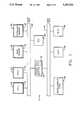
- FIG. 1is a block diagram of a general computer system incorporating the present invention
- FIGS. 2A, 21, and 2Care a more detailed schematic diagram of the shift register logic circuitry located on the processor boards, memory boards, and system board of FIG. 1 according to the present invention
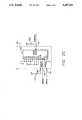
- FIG. 3is a schematic logic diagram of the MEMID ports and associated circuitry in the SGC of FIG. 2A according to the present invention.
- FIG. 4is a timing diagram of the circuitry of FIG. 3.
- the letter Crefers to a personal computer system that includes an apparatus for system configuration determination according to the present invention.
- the personal computer system Cincludes a primary central processor board referred to as CPU1 20 attached to a host bus 22 through a slot 33.
- the CPU1 20includes a series of permanently enabled signals which identify the board as a processor board and identify the particular processor type and configuration.
- the host bus 22includes an address bus, a data bus, and various control lines.
- the host bus 22also includes a series of option slots 34, 36, and 38 into which memory boards or an additional processor board may be placed. However, the use of additional processor or memory expansion slots is also contemplated.
- the expansion slots 36 and 38may include either base or expansion memory boards, and the remaining option slot 34 may include either a base or expansion memory board or a secondary processor board.
- a base memory board 26 and an expansion memory board 28are connected to the host bus 22 through the expansion slots 36 and 38, respectively, and a secondary microprocessor board referred to as the CPU2 24 is configured in the remaining expansion slot 34.
- the base memory board 26 and the expansion memory board 28have a series of connectors for addition of memory modules.
- Each memory module that is placed in the base memory board 26 and expansion memory board 28include a series of permanently enabled signals to indicate the amount of memory installed on the module. If no memory module is installed in a given connector, the signals associated with that connector are set at a predefined level.
- the CPU2 24includes a series of permanently enabled signals which identify the board as a processor board and identify the particular processor type and configuration.
- the host bus 22is connected through a block circuit 40 comprising various system control logic 32 and buffers to an input/output bus referred to as the Extended Industry Standard Architecture (EISA) bus 42.
- the EISA bus 42is an extension of the Industry Standard Architecture (ISA) bus, which was used in the International Business Machines (IBM) AT personal computers.
- ISAIndustry Standard Architecture
- the EISA bus 42includes several slots 44 and 45 for various input/output devices, as well as a block circuit 48 which includes numerous miscellaneous logic that is necessary for operation of the EISA bus 42.
- the system board logic 32, the CPU1 20, the CPU2 24 and each of the memory boards 26 and 28 that are configured within the system Chave associated with them shift registers that receive identification and configuration data according to the present invention.
- the shift registers used in FIGS. 2A, 2B and 2C according to the present inventionare 8-bit parallel load, serial in shift registers that include a serial input and a serial output.
- Each shift registerincludes a shift load input referred to as S/L.
- the shift registerserially shifts its contents when the S/L input receives a logic high value and parallel loads the signals at its inputs when the S/L input receives a logic low value.
- Each of the shift registersalso includes a clock input and a clock inhibit input.
- the clock inhibit input of each of the shift registersis represented as an inverted clock enable or CE input in FIGS. 2A, 2B, and 2C, and this input operates such that when it is held low with the S/L input high, the clock input of the shift register is enabled.
- the system board logic 32includes an 8-bit parallel load, serial in, serial out shift register 100 which is used to identify the type of board present in each of the respective expansion slots 34, 36, and 38 of the system C.
- the shift register 100receives two identification signals from the respective board present in each of the respective slots 33, 34, 36, and 38. These identification signals indicate whether a primary processor, a secondary processor, a base memory board, or an expansion memory board is configured in the respective slots 33, 34, 36, and 38. If no board is present in a respective expansion slot 34, 36, or 38, then pull-up resistors connected to the respective shift register inputs pull the respective identification signal input values to a high logic value, which indicates that the respective slot is empty.
- the shift register 100receives two identification signals from each of the CPU1 20, the CPU2 24, the base memory board 26, and the expansion memory board 28 according to the preferred embodiment. Different logic levels are provided on the respective identification signals to indicate base memory, expansion memory, and processor boards.
- Two signals referred to as P1TYPE1 and P1TYPE0are provided from expansion slot 33 and are connected to the D7 and D6 inputs, respectively, of the shift register 100.
- the P1TYPE1 and P1TYPE0 signalsprovide information on the type of CPU1 configured within the system C.
- Two signals referred to as P2TYPE1 and P2TYPE0are provided from expansion slot 34 and are connected to the D5 and D4 inputs, respectively, of the shift register 100.
- the P2TYPE1 and P2TYPE0 signalshave logic values which indicate if a memory board or preferably a secondary processor board is configured in the respective expansion slot 34.
- Pull-up resistors 202 and 204are also connected to the D5 and D4 inputs, respectively, of the shift register 100. Therefore, if there is no secondary processor board or memory board configured in the expansion slot 34, the D5 and D4 inputs of shift register 100 are at a logic high value, which indicates that the expansion slot 34 is empty.
- the D7 and D6 inputs of the shift register 100are not connected to pull-up resistors because the CPU1 20 is not an optional part of the computer system C but rather is the primary microprocessor and therefore is required to be present in the computer system C according to the preferred embodiment.
- an alternate design of the shift register 100 for a multiple processor computer system c in which no single processor is designated as a primary processoris also contemplated.
- Two signals referred to as XMTYPE1 and XMTYPE0are provided from expansion slot 38 and are connected to the D3 and D2 inputs, respectively, of the shift register 100.
- the XNTYPE1 and XMTYPE0 signalshave logic values which indicate that a memory board, preferably an expansion memory board, 28 is configured in the respective expansion slot 38.
- Pull-up resistors 206 and 208are connected to the D3 and D2 inputs, respectively, of the shift register 100. Therefore, if there is no memory board present within the expansion slot 38, then the D3 and D2 inputs are at a logic high value, which indicates that the respective expansion slot 38 is empty.
- BMTYPE1 and BMTYPE0Two signals referred to as BMTYPE1 and BMTYPE0 are provided from expansion slot 36 and are connected to the D1 and D0 inputs, respectively, of the shift register 100.
- the BMTYPE1 and BMTYPE0 signalshave logic values which indicate that a base memory board 26 is configured in the respective expansion slot 36.
- Pull-up resistors 210 and 212are connected to the D1 and D0 inputs, respectively, of the shift register 100. Therefore, if there is no memory board present within the expansion slot 36, the D1 and Do inputs are at a logic high value, which indicates that the respective expansion slot 36 is empty.
- the QMSB or serial output of the shift register 100is connected to an input of the SGC 30 referred to as the DATAIN input.
- a serial out signal referred as P1SEROUT from slot 33is connected to the serial input SLIN of the shift register 100.
- a memory identification load signal referred to as MIDLD*is connected to the S/L input of the shift register 100.
- a clock signal referred to as MIDCLKis connected to the clock input of the shift register 100.
- the MIDCLK signalhas eight clock pulses each time a memory identification port in the SGC 30 is accessed.
- the MIDCLK signal and the MIDLD* signalare both generated by the SGC 30, and the generation of these signals is explained in greater detail below.
- the inverted CE input of the shift register 100is tied to a logic low value.
- each clock pulse of the MIDCLK signalserially shifts upward the contents of the shift register 100.
- the content of the D7 locationis shifted to the DATAIN input of the SGC 30, and the signal value at the SLIN input of the shift register 100 is shifted into the D0 location of the shift register 100.
- the resultant effectis to serially shift the contents of the shift register 100 to the DATAIN input of the SGC 30.
- CPU1 20is located in slot 33
- CPU2 24is located in slot 34
- base memory board 26is located in slot 36
- an expansion memory boardis located in slot 38. It is noted that the only requirements for location in the preferred embodiment are CPU1 20 in slot 33, CPU2 24 in slot 34, if present, and a base memory board 26 in slot 36, if present.
- a base memory board 26 or an expansion memory board 28may be installed in slots 34 or 38.
- the CPU1 20includes a shift register 102 whose D inputs are connected to predetermined logic values that provide information on the type of CPU1 20 that is configured within the system C.
- the inverted clear enable or CE input of the shift register 102is connected to a logic low value.
- the MIDCLK signalis connected to the clock input of the shift register 102, and the MIDLD* signal is connected to the S/L input of the shift register 102.
- the D3, D4, D5, D6 and D7 inputs of the shift register 102are connected to a logic low value and the D0, D1 and D2 inputs are connected to a logic high value.
- This configuration of predetermined valuespreferably represents that an Intel Corporation (Intel) 80386 microprocessor is the microprocessor present on the particular processor board that serves as the CPU1 20, but the use of different predetermined signal values and/or the use of other microprocessors as the primary processor CPU1 20 is also contemplated.
- Intel Corporation 80386 microprocessoris the microprocessor present on the particular processor board that serves as the CPU1 20, but the use of different predetermined signal values and/or the use of other microprocessors as the primary processor CPU1 20 is also contemplated.
- the QMSB or serial output of the shift register 102forms the P1SEROUT signal, which is connected to the SLIN input of the system board shift register 100. Therefore, the processor type information for the CPU1 20 is serially shifted to the system board shift register 100, beginning with the first MIDCLK signal clock pulse.
- the serial or SLIN input of the shift register 102is connected to a base memory serial output signal referred to as BMSEROUT.
- the base memory board 26includes two shift registers 110 and 112 which are used to receive the memory information from each of the respective memory modules which can be placed on the base memory board 26.
- the MIDLD* signalis connected to the S/L input of each of the shift registers 110 and 112.
- the inverted clear enable or CE inputsare connected to logic low values.
- the MIDCLK signalis connected to the clock inputs of each of the shift registers 110 and 112.
- the D inputs of each of the shift register 110 and 112are connected to the appropriate memory module configuration signals, which are not shown for clarity, that are provided by each of the respective memory modules that are attached to the base memory board 26. Because the generation of these memory configuration signals is well known to those skilled in the art, their description has been omitted for the purpose of clarity.
- the QMSB serial output of the shift register 112is connected to the SLIN input of the shift register 110.
- the QMSB or serial output of the shift register 110forms the BMSEROUT signal, which is connected to the SLIN input of the CPU1 shift register 102 (FIG. 2A).
- An expansion memory board serial output signal referred to as XMSEROUTis connected to the SLIN input of the shift register 112.
- the XMSEROUT signalis also connected to the input of a tristate buffer 130 located on the host bus 22.
- the output of the tristate buffer 130is connected to the BMSEROUT signal.
- the enable input of the tri-state buffer 130is connected to a pull-up resistor 131 and is also connected to a logic low value generated by the base memory board 26. Therefore, if the base memory board 26 is not present within the expansion slot 36, the tristate buffer 130 is enabled, allowing the base memory shift registers 110 and 112 to be excluded from the daisy chain, and the XMSEROUT signal is shunted to the BMSEROUT signal. If the base memory board 26 is present within the expansion slot 36, then the tristate buffer 130 is disabled, and the base memory shift registers 110 and 112 are included in the daisy chain and act to serially shift the base memory configuration signals to the CPU1 shift register 102.
- the expansion memory board 28includes three shift registers 120, 122 and 124 according to the present invention that store the respective memory module configuration information from the memory modules located on the expansion memory board 28. Three shift registers are used on the expansion memory board 28 in the preferred embodiment because the expansion memory board 28 can receive more memory modules than can the preferred base memory board 26.
- the MIDLD* signalis connected to the S/L input of each of the shift registers 120, 122 and 124.
- the inverted CE input of each of the shift registers 120, 122, and 124is connected to a logic low value and the MIDCLK signal is connected to the clock inputs of each of the shift registers 120, 122, and 124.
- the D inputs of each of the shift registers 120, 122, and 124receive memory module configuration signals (not shown) that are output from each of the respective memory modules located on the expansion memory board 28.
- the QMSB serial output of the shift register 124is connected the SLIN input of the shift register 122, and the QMSB serial output of the shift register 122 is connected to the SLIN input of the shift register 120.
- the QMSB serial output of the shift register 120is the XMSEROUT signal, which is connected to the base memory board shift register 112.
- a CPU2 serial output signal referred to as P2SEROUTis connected to the SLIN input of the shift register 124.
- the P2SEROUT signalis output from a shift register that is associated with the secondary processor CPU2 24 that is configured within the expansion slot 34 of the system C according to the preferred embodiment.
- the P2SEROUT signalis also connected to the input of a tristate buffer 140 located on the host bus 22.
- the output of the tri-state buffer 140is connected to the XMSEROUT signal.
- the enable input of the tristate buffer 140is connected to a pull-up resistor 141 and is also connected to a logic low value generated by the expansion memory board 28.
- the tristate buffer 140is enabled, allowing for the expansion memory shift registers 120, 122, and 124 to be excluded from the daisy chain, and the P2SEROUT signal is directly shunted to the XMSEROUT signal. If the expansion memory board 28 is present within the expansion slot 38, then the tristate buffer 140 is disabled, and the shift registers 120, 122, and 124 are included in the daisy chain.
- the CPU2 24includes a shift register 142 whose D inputs are connected to certain predetermined logic values that provide information on the type of microprocessor present on the processor board serving as the secondary microprocessor CPU2 24.
- the D3, D5, D6 and D7 inputs to the shift register 142are tied to a logic low value and the D0, D1, D2 and D4 inputs are tied to a logic high value.
- This configuration of predetermined logic valuespreferably represents that an Intel 80486 microprocessor is configured as the secondary processor CPU2 24, but the use of different predetermined signal values and/or the use of other microprocessors as the secondary processor CPU2 20 is also contemplated.
- the inverted clear enable or CE input of the shift register 102is tied to a logic low value.
- the MIDCLK signalis connected to the clock input of the shift register 142, and the MIDLD* signal is connected to the S/L input.
- the QMSB or serial output of the shift register 142forms the P2SEROUT signal, which is connected to the SLIN input of the expansion memory board shift register 124. Therefore, the processor type information for the CPU2 24 is serially shifted to the expansion memory board shift register 124 beginning with the first MIDCLK signal clock pulse.
- a pull-up resistor 220is connected to the output generated by the expansion slot 34, which is the P2SEROUT signal generated by the CPU2 shift register 142. Therefore, if the CPU2 24 or any other type of memory board is not present within the expansion slot 34, then the output provided by the expansion slot 34 is a logic high value.
- the SLIN input of the CPU2 shift register 142is set through slot 34 to a logical high value provided by a resistor 141.
- the resistor 141is preferably located on the system board so that the processor boards are full interchangeable in the processor slots. In this way, logic high values are shifted into the CPU2 shift register 142 beginning with the first MIDCLK signal.
- the system board shift register 100, the CPU1 shift register 102, the base memory board shift registers 110 and 112, the expansion memory board shift registers 120, 122, and 124 and the CPU2 shift register 142parallel load their respective identification or configuration data on their respective D inputs.
- the MIDCLK signalthen begins a sequence of 8 clock pulses, which serially shifts the data located in a respective shift register to the next successive shift register in the daisy chain.
- the data located in the system board shift register 100is serially shifted into the memory identification port inside the SGC 30. In this way, the system configuration data loaded in each of the shift registers 100, 102, 110, 112, 120, 122 124, and 142 is serially shifted into the memory identification port inside the SGC eight bits at a time.
- additional expansion slotsin the computer system C where additional processor or memory boards could be placed.
- These additional expansion slotscould be located between the CPU1 20 and the last expansion slot 34 in the daisy chain or other locations as desired.
- Additional processor or memory boardswould be placed in these additional expansion slots in the daisy chain, and these boards would include shift registers similar to those described above according to the present invention. Additional shift registers could be present on the system board to receive presence and identification information from these additional slots.
- the SGC 30includes memory module identification ports referred to as the MEMID data port and the MEMID control port.
- the MEMID control portgenerates the MIDLD* signal, which controls the loading of the configuration and identification data into the various shift registers 100, 102, 110, 112, 120, 122, 124, and 142 discussed above.
- the MEMID data portserially receives the system configuration data from the various shift registers 100, 102, 110, 112, 120, 122, 124, and 142 associated with the system board 32, the CPU1 20, the CPU2 24, the base memory board 26, the expansion memory board 28, and the CPU2 24, respectively.
- the MEMID data portstores this data into appropriate 4 bit serial in, parallel out shift registers 150 and 152. These shift registers 150 and 152 then transmit the data in parallel to the system C so that it can determine the processor type and memory configuration of the system C.
- the system CWhen the system configuration is to be determined, the system C, preferably the CPU1 20, writes a value to a bit in the MEMID control port which asserts the MIDLD* signal.
- the MEMID control portis preferably located at port address OC64h.
- a decoded address signal for port address OC64h referred to as PC64E* and an I/O write strobe signal referred to as IOW*are connected to the inputs of a 2-input NOR gate 390.
- the output of the NOR gate 390 and bit 0 of the data bus referred to as DI ⁇ 0>are connected to the inputs of a 2-input NAND gate 392 whose output is the MIDLD* signal.
- the MIDLD* signalis asserted low for one cycle. This parallel loads the respective identification and configuration data into the respective shift registers 100, 102, 110, 112, 120, 122 and 124.
- the system Ccan begin reading the data from the MEMID data port to receive the memory configuration information.
- the DATAIN input of the SGC 30is connected to the D or serial in input of the shift register 150.
- the Q0, Q1, Q2 and Q3 outputs of the shift register 150form the four low order bits of the MEMID data port.
- the Q3 output of the shift register 150is also connected to a series of delay circuits 154 to the D or serial in input of the second shift register 152.
- the Q0, Q1, Q2 and Q3 outputs of the shift register 152form the four high order bits of the MEMID data port.
- the clock inputs of the shift registers 150 and 152are connected to the MIDCLK signal.
- a signal referred to as PC63Eis the decoded port address signal for the MEMID data port, which is preferably located at port address OC63h.
- the PC63E signalis connected to the input of a 2-input NAND gate 400.
- the EISA timing signal referred to as CMD*is connected to the other input of the 2-input NAND gate 400, whose output in turn is connected to the inverted reset input of a 4 bit binary counter 402.
- the MIDCLK signalis connected to the clock input of the 4 bit binary counter 402.
- the Q3 output of the counter 402is a data busy signal referred to as DATABSY. As shown in FIG.
- the DATABSY signalis negated or a logic low value when the MEMID data port is read, signified by the CMD* signal being asserted low, and the DATABSY signal remains a logical low value for eight MIDCLK signal cycles. Therefore, the 4 bit binary counter 402 serves the function of counting out eight successive serial shifts of data from the system board shift register 100 into the MEMID data port.
- the PC63E signalis also connected to the input of an inverter 406 whose output is a signal referred to as PC63E*.
- the PC63E* signal, the DATABSY signal and a latched write/read signal referred to as WRL, which is high when indicating a write operation is in progress and low when indicating a read operation is in progress,are connected to the inputs of a 3 input OR gate 410.
- the output of the 3-input OR gate 410is a ready signal referred to as EXRDYM, which is buffered and synchronized by portions of the SGC 30 not shown and connected to the EXRDY signal present on the EISA bus 42. When the EXRDY signal is low, this is an indication that the particular location being addressed is not ready.
- the EXRDYM signalremains low during a read to the MEMID data port while the DATABSY signal is negated low.
- the EXRDYM signaltherefore remains negated or low for eight MIDCLK signal cycles, which acts to extend the length of the bus cycle, thereby allowing eight bits of data to be shifted into the MEMID data port from the system board shift register 100.
- the EXRDYM signal and the CMD* signalare connected to the inputs of a 2-input NOR gate 412 whose output is connected to the D input of a D-type flip-flop 420.
- a clock signal referred to as CKis connected to the clock input of the flip-flop 420.
- the CK signalhas a frequency of 14.32 MHz, but the use of other frequencies is also contemplated.
- the CK signalis also connected to the input of an inverter 422 whose output is connected to one input of a 2-input AND gate 424.
- the Q output of the flip-flop 420is connected to the other input of the 2-input AND gate 424, whose output is the MIDCLK signal.
- the MIDCLK signalis a logical low value until one CK signal cycle after both the EXRDYM signal and the CMD* signal are asserted low, after which time the MIDCLK signal mirrors the CK signal for eight cycles.
- the MIDCLK signalis developed as a clocking signal during a read to the MEMID data port in order to clock eight bits of data from the system board shift register 100 into the MEMID data port.
- the EXRDYM signalis negated low to extend the bus cycle until eight bits of data are clocked into the MEMID port from the system board shift register 100.
- the datais driven onto the host bus 22 to the CPU1 20, and the EXRDYM signal is asserted high.
- the system Ccan then read the next byte on the ensuing cycle, and this process can repeat itself until all of the memory and processor configuration data resident in the various shift registers 100, 102, 110, 112, 120, 122, 124, and 142 has been read by the CPU1 20.
- FIG. 4a timing diagram for the MEMID data port is shown.
- the DATABSY signalis negated low, which in turn forces the EXRDY signal to be negated low.
- Thisactivates the MIDCLK signal, and the data signals from the system board shift register 100 are subsequently shifted into the MEMID port through the DATAIN input on each rising edge of the MIDCLK signal.
- the DATABSY signalis asserted high, forcing the EXRDY signal to be negated high and stopping production of the MIDCLK signal on the next rising edge of the CK signal.
- the eight bits of dataare then driven onto the data bus on the host bus 22 through data buffers (not shown).
- the system Cthen can continue reading the next byte on the subsequent cycle if desired, or proceed to other operations if all of the identification and configuration information has been received.
- processor type and memory configuration in the computer system Cis determined through the use of one 8 bit data port and no addressing capability to the respective processor or memory boards is necessary for this purpose.
- shift registers located on each processor and memory boardare used to transfer the data in a serial fashion to the 8 bit MEMID data port.
- the serial configuration of the shift registers and the use of tristate buffersallows this configuration to recognize and account for expansion slots where no processor or memory board has been asserted.
Landscapes
- Engineering & Computer Science (AREA)
- Theoretical Computer Science (AREA)
- Physics & Mathematics (AREA)
- General Engineering & Computer Science (AREA)
- General Physics & Mathematics (AREA)
- Multi Processors (AREA)
Abstract
Description
Claims (8)
Priority Applications (1)
| Application Number | Priority Date | Filing Date | Title |
|---|---|---|---|
| US07/606,165US5287531A (en) | 1990-10-31 | 1990-10-31 | Daisy-chained serial shift register for determining configuration of removable circuit boards in a computer system |
Applications Claiming Priority (1)
| Application Number | Priority Date | Filing Date | Title |
|---|---|---|---|
| US07/606,165US5287531A (en) | 1990-10-31 | 1990-10-31 | Daisy-chained serial shift register for determining configuration of removable circuit boards in a computer system |
Publications (1)
| Publication Number | Publication Date |
|---|---|
| US5287531Atrue US5287531A (en) | 1994-02-15 |
Family
ID=24426838
Family Applications (1)
| Application Number | Title | Priority Date | Filing Date |
|---|---|---|---|
| US07/606,165Expired - LifetimeUS5287531A (en) | 1990-10-31 | 1990-10-31 | Daisy-chained serial shift register for determining configuration of removable circuit boards in a computer system |
Country Status (1)
| Country | Link |
|---|---|
| US (1) | US5287531A (en) |
Cited By (70)
| Publication number | Priority date | Publication date | Assignee | Title |
|---|---|---|---|---|
| US5454081A (en)* | 1992-08-28 | 1995-09-26 | Compaq Computer Corp. | Expansion bus type determination apparatus |
| US5491805A (en)* | 1991-05-03 | 1996-02-13 | D2B Systems Company Limited | Apparatus for automatically identifying point-to-point cable interconnections among a plurality of components which are also linked via a broadcast control channel |
| US5509138A (en)* | 1993-03-22 | 1996-04-16 | Compaq Computer Corporation | Method for determining speeds of memory modules |
| US5530887A (en)* | 1991-02-22 | 1996-06-25 | International Business Machines Corporation | Methods and apparatus for providing automatic hardware device identification in computer systems that include multi-card adapters and/or multi-card planar complexes |
| US5548782A (en)* | 1993-05-07 | 1996-08-20 | National Semiconductor Corporation | Apparatus for preventing transferring of data with peripheral device for period of time in response to connection or disconnection of the device with the apparatus |
| EP0735478A1 (en)* | 1995-03-31 | 1996-10-02 | BULL HN INFORMATION SYSTEMS ITALIA S.p.A. | Variable configuration data processing system with automatic serial test interface connection configuration and bypass device |
| WO1996031086A1 (en)* | 1995-03-31 | 1996-10-03 | Anthony Hooley | Improvements in or relating to loudspeakers |
| US5568651A (en)* | 1994-11-03 | 1996-10-22 | Digital Equipment Corporation | Method for detection of configuration types and addressing modes of a dynamic RAM |
| US5594925A (en)* | 1993-01-05 | 1997-01-14 | Texas Instruments Incorporated | Method and apparatus determining order and identity of subunits by inputting bit signals during first clock period and reading configuration signals during second clock period |
| US5617081A (en)* | 1991-07-31 | 1997-04-01 | 3Com Corporation | Method and apparatus for live insertion and removal of electronic sub-assemblies |
| US5675748A (en)* | 1993-12-21 | 1997-10-07 | Object Technology Licensing Corp. | Method and apparatus for automatically configuring computer system hardware and software |
| US5675825A (en)* | 1992-08-31 | 1997-10-07 | Intel Corporation | Apparatus and method for identifying a computer microprocessor |
| US5701420A (en)* | 1994-07-20 | 1997-12-23 | Intel Corporation | Method for initializing an array of configurable components |
| US5713006A (en)* | 1995-03-15 | 1998-01-27 | Texas Instruments Incorporated | Electronic device and method for selective enabling of access to configuration registers used by a memory controller |
| US5734845A (en)* | 1993-05-28 | 1998-03-31 | Fujitsu Limited | Bus arbiter provided in a multi-processor system |
| US5745791A (en)* | 1992-09-16 | 1998-04-28 | Intel Corporation | System for interfacing first and second components having different data path width by generating first and second component address to read data into buffer |
| US5796639A (en)* | 1996-09-19 | 1998-08-18 | Intel Corporation | Method and apparatus for verifying the installation of strapping devices on a circuit board assembly |
| US5802074A (en)* | 1996-09-19 | 1998-09-01 | Intel Corporation | Method and apparatus for the non-invasive testing of printed circuit board assemblies |
| US5835738A (en)* | 1994-06-20 | 1998-11-10 | International Business Machines Corporation | Address space architecture for multiple bus computer systems |
| US5848250A (en)* | 1993-04-01 | 1998-12-08 | Packard Bell Nec | Processor upgrade system for a personal computer |
| US5862320A (en)* | 1995-12-22 | 1999-01-19 | Cirrus Logic, Inc. | SDRAM DIMM presence detect interface |
| US5915128A (en)* | 1997-01-29 | 1999-06-22 | Unisys Corporation | Serial speed-matching buffer utilizing plurality of registers where each register selectively receives data from transferring units or sequentially transfers data to another register |
| US6182159B1 (en)* | 1995-09-19 | 2001-01-30 | Ricoh Company, Ltd. | System for detachably connecting memory cards which provide memory specified by predetermined range of addresses registered in list and updating list independent of the I/O operation |
| EP0911223A3 (en)* | 1997-10-21 | 2001-03-14 | Trw Inc. | Occupant restraint system having serially connected devices |
| US20040151325A1 (en)* | 2001-03-27 | 2004-08-05 | Anthony Hooley | Method and apparatus to create a sound field |
| US20050041530A1 (en)* | 2001-10-11 | 2005-02-24 | Goudie Angus Gavin | Signal processing device for acoustic transducer array |
| US20050089182A1 (en)* | 2002-02-19 | 2005-04-28 | Troughton Paul T. | Compact surround-sound system |
| US20050144383A1 (en)* | 2003-12-25 | 2005-06-30 | Seiichi Higaki | Memory control device and method for controlling the same |
| US20060026349A1 (en)* | 2004-07-30 | 2006-02-02 | International Business Machines Corporaiton | System, method and storage medium for providing a serialized memory interface with a bus repeater |
| US20060036826A1 (en)* | 2004-07-30 | 2006-02-16 | International Business Machines Corporation | System, method and storage medium for providing a bus speed multiplier |
| US20060095646A1 (en)* | 2004-10-29 | 2006-05-04 | International Business Machines Corporation | System, method and storage medium for a memory subsystem command interface |
| US20060095703A1 (en)* | 2004-10-29 | 2006-05-04 | International Business Machines Corporation | System, method and storage medium for bus calibration in a memory subsystem |
| US20060095620A1 (en)* | 2004-10-29 | 2006-05-04 | International Business Machines Corporation | System, method and storage medium for merging bus data in a memory subsystem |
| US20060095701A1 (en)* | 2004-10-29 | 2006-05-04 | International Business Machines Corporation | System, method and storage medium for a memory subsystem with positional read data latency |
| US20060107175A1 (en)* | 2004-10-29 | 2006-05-18 | International Business Machines Corporation | System, method and storage medium for providing fault detection and correction in a memory subsystem |
| US20060107186A1 (en)* | 2004-10-29 | 2006-05-18 | International Business Machines Corporation | System, method and storage medium for providing a high speed test interface to a memory subsystem |
| US20060117233A1 (en)* | 2004-10-29 | 2006-06-01 | International Business Machines Corporation | System, Method and storage medium for testing a memory module |
| US20060136618A1 (en)* | 2004-07-30 | 2006-06-22 | International Business Machines Corporation | System, method and storage medium for a multi-mode memory buffer device |
| US20060153391A1 (en)* | 2003-01-17 | 2006-07-13 | Anthony Hooley | Set-up method for array-type sound system |
| US20060164909A1 (en)* | 2005-01-24 | 2006-07-27 | International Business Machines Corporation | System, method and storage medium for providing programmable delay chains for a memory system |
| KR100617678B1 (en)* | 1998-08-13 | 2007-04-25 | 삼성전자주식회사 | Serial Numbering System and Method for Daisy-Chained Systems |
| US20070101086A1 (en)* | 2005-10-31 | 2007-05-03 | International Business Machines Corporation | System, method and storage medium for deriving clocks in a memory system |
| US7224595B2 (en) | 2004-07-30 | 2007-05-29 | International Business Machines Corporation | 276-Pin buffered memory module with enhanced fault tolerance |
| US20070160053A1 (en)* | 2005-11-28 | 2007-07-12 | Coteus Paul W | Method and system for providing indeterminate read data latency in a memory system |
| US20070223763A1 (en)* | 2003-09-16 | 2007-09-27 | 1... Limited | Digital Loudspeaker |
| US7277988B2 (en) | 2004-10-29 | 2007-10-02 | International Business Machines Corporation | System, method and storage medium for providing data caching and data compression in a memory subsystem |
| US20070269071A1 (en)* | 2004-08-10 | 2007-11-22 | 1...Limited | Non-Planar Transducer Arrays |
| US20070276977A1 (en)* | 2006-05-24 | 2007-11-29 | International Business Machines Corporation | Systems and methods for providing memory modules with multiple hub devices |
| US20070276976A1 (en)* | 2006-05-24 | 2007-11-29 | International Business Machines Corporation | Systems and methods for providing distributed technology independent memory controllers |
| US20080034148A1 (en)* | 2006-08-01 | 2008-02-07 | International Business Machines Corporation | Systems and methods for providing performance monitoring in a memory system |
| US20080040563A1 (en)* | 2006-08-10 | 2008-02-14 | International Business Machines Corporation | Systems and methods for memory module power management |
| US20080098277A1 (en)* | 2006-10-23 | 2008-04-24 | International Business Machines Corporation | High density high reliability memory module with power gating and a fault tolerant address and command bus |
| US20080094811A1 (en)* | 2006-10-23 | 2008-04-24 | International Business Machines Corporation | High density high reliability memory module with a fault tolerant address and command bus |
| US20080115137A1 (en)* | 2006-08-02 | 2008-05-15 | International Business Machines Corporation | Systems and methods for providing collision detection in a memory system |
| US20080162991A1 (en)* | 2007-01-02 | 2008-07-03 | International Business Machines Corporation | Systems and methods for improving serviceability of a memory system |
| US20080183903A1 (en)* | 2007-01-29 | 2008-07-31 | International Business Machines Corporation | Systems and methods for providing dynamic memory pre-fetch |
| US7441060B2 (en) | 2004-10-29 | 2008-10-21 | International Business Machines Corporation | System, method and storage medium for providing a service interface to a memory system |
| US7490217B2 (en) | 2006-08-15 | 2009-02-10 | International Business Machines Corporation | Design structure for selecting memory busses according to physical memory organization information stored in virtual address translation tables |
| US20090119114A1 (en)* | 2007-11-02 | 2009-05-07 | David Alaniz | Systems and Methods for Enabling Customer Service |
| US7539842B2 (en) | 2006-08-15 | 2009-05-26 | International Business Machines Corporation | Computer memory system for selecting memory buses according to physical memory organization information stored in virtual address translation tables |
| US7539800B2 (en) | 2004-07-30 | 2009-05-26 | International Business Machines Corporation | System, method and storage medium for providing segment level sparing |
| US7577260B1 (en) | 1999-09-29 | 2009-08-18 | Cambridge Mechatronics Limited | Method and apparatus to direct sound |
| US7581073B2 (en) | 2006-08-09 | 2009-08-25 | International Business Machines Corporation | Systems and methods for providing distributed autonomous power management in a memory system |
| US7584336B2 (en) | 2006-06-08 | 2009-09-01 | International Business Machines Corporation | Systems and methods for providing data modification operations in memory subsystems |
| US7606988B2 (en) | 2007-01-29 | 2009-10-20 | International Business Machines Corporation | Systems and methods for providing a dynamic memory bank page policy |
| US20090296964A1 (en)* | 2005-07-12 | 2009-12-03 | 1...Limited | Compact surround-sound effects system |
| US7636813B2 (en) | 2006-05-22 | 2009-12-22 | International Business Machines Corporation | Systems and methods for providing remote pre-fetch buffers |
| US7895331B1 (en) | 2006-08-10 | 2011-02-22 | Bivio Networks, Inc. | Method for dynamically configuring network services |
| US20110129101A1 (en)* | 2004-07-13 | 2011-06-02 | 1...Limited | Directional Microphone |
| US8005101B1 (en)* | 2006-08-10 | 2011-08-23 | Bivio Networks, Inc. | Scalable architecture for deep-packet processing |
Citations (4)
| Publication number | Priority date | Publication date | Assignee | Title |
|---|---|---|---|---|
| US4313159A (en)* | 1979-02-21 | 1982-01-26 | Massachusetts Institute Of Technology | Data storage and access apparatus |
| US4617566A (en)* | 1983-12-15 | 1986-10-14 | Teleplex Corporation | Addressable-port, daisy chain telemetry system with self-test capability |
| US5027313A (en)* | 1988-08-25 | 1991-06-25 | Compaq Computer Corporation | Apparatus for determining maximum usable memory size |
| US5056015A (en)* | 1988-03-23 | 1991-10-08 | Du Pont Pixel Systems Limited | Architectures for serial or parallel loading of writable control store |
- 1990
- 1990-10-31USUS07/606,165patent/US5287531A/ennot_activeExpired - Lifetime
Patent Citations (4)
| Publication number | Priority date | Publication date | Assignee | Title |
|---|---|---|---|---|
| US4313159A (en)* | 1979-02-21 | 1982-01-26 | Massachusetts Institute Of Technology | Data storage and access apparatus |
| US4617566A (en)* | 1983-12-15 | 1986-10-14 | Teleplex Corporation | Addressable-port, daisy chain telemetry system with self-test capability |
| US5056015A (en)* | 1988-03-23 | 1991-10-08 | Du Pont Pixel Systems Limited | Architectures for serial or parallel loading of writable control store |
| US5027313A (en)* | 1988-08-25 | 1991-06-25 | Compaq Computer Corporation | Apparatus for determining maximum usable memory size |
Cited By (152)
| Publication number | Priority date | Publication date | Assignee | Title |
|---|---|---|---|---|
| US5530887A (en)* | 1991-02-22 | 1996-06-25 | International Business Machines Corporation | Methods and apparatus for providing automatic hardware device identification in computer systems that include multi-card adapters and/or multi-card planar complexes |
| US5491805A (en)* | 1991-05-03 | 1996-02-13 | D2B Systems Company Limited | Apparatus for automatically identifying point-to-point cable interconnections among a plurality of components which are also linked via a broadcast control channel |
| US5617081A (en)* | 1991-07-31 | 1997-04-01 | 3Com Corporation | Method and apparatus for live insertion and removal of electronic sub-assemblies |
| US5454081A (en)* | 1992-08-28 | 1995-09-26 | Compaq Computer Corp. | Expansion bus type determination apparatus |
| US5958037A (en)* | 1992-08-31 | 1999-09-28 | Intel Corporation | Apparatus and method for identifying the features and the origin of a computer microprocessor |
| US5790834A (en)* | 1992-08-31 | 1998-08-04 | Intel Corporation | Apparatus and method using an ID instruction to identify a computer microprocessor |
| US5794066A (en)* | 1992-08-31 | 1998-08-11 | Intel Corporation | Apparatus and method for identifying the features and the origin of a computer microprocessor |
| US5675825A (en)* | 1992-08-31 | 1997-10-07 | Intel Corporation | Apparatus and method for identifying a computer microprocessor |
| US5745791A (en)* | 1992-09-16 | 1998-04-28 | Intel Corporation | System for interfacing first and second components having different data path width by generating first and second component address to read data into buffer |
| US5594925A (en)* | 1993-01-05 | 1997-01-14 | Texas Instruments Incorporated | Method and apparatus determining order and identity of subunits by inputting bit signals during first clock period and reading configuration signals during second clock period |
| US5509138A (en)* | 1993-03-22 | 1996-04-16 | Compaq Computer Corporation | Method for determining speeds of memory modules |
| US5848250A (en)* | 1993-04-01 | 1998-12-08 | Packard Bell Nec | Processor upgrade system for a personal computer |
| US5548782A (en)* | 1993-05-07 | 1996-08-20 | National Semiconductor Corporation | Apparatus for preventing transferring of data with peripheral device for period of time in response to connection or disconnection of the device with the apparatus |
| US5734845A (en)* | 1993-05-28 | 1998-03-31 | Fujitsu Limited | Bus arbiter provided in a multi-processor system |
| US5675748A (en)* | 1993-12-21 | 1997-10-07 | Object Technology Licensing Corp. | Method and apparatus for automatically configuring computer system hardware and software |
| US5835738A (en)* | 1994-06-20 | 1998-11-10 | International Business Machines Corporation | Address space architecture for multiple bus computer systems |
| US5701420A (en)* | 1994-07-20 | 1997-12-23 | Intel Corporation | Method for initializing an array of configurable components |
| US5568651A (en)* | 1994-11-03 | 1996-10-22 | Digital Equipment Corporation | Method for detection of configuration types and addressing modes of a dynamic RAM |
| US5805854A (en)* | 1995-03-15 | 1998-09-08 | Texas Instruments Incorporated | System and process for memory column address organization in a computer system |
| US5724553A (en)* | 1995-03-15 | 1998-03-03 | Texas Instruments Incorporated | Electronic system with circuitry for generating memory column addresses using memory array type bits in a control register |
| US5737563A (en)* | 1995-03-15 | 1998-04-07 | Texas Instruments Incorporated | Determination of memory bank sizes in a computer system |
| US5778425A (en)* | 1995-03-15 | 1998-07-07 | Texas Instruments Incorporated | Electronic system having a first level write through cache memory and smaller second-level write-back cache memory and method of operating the same |
| US5737765A (en)* | 1995-03-15 | 1998-04-07 | Texas Instruments Inc | Electronic system with circuitry for selectively enabling access to configuration registers used by a memory controller |
| US5737748A (en)* | 1995-03-15 | 1998-04-07 | Texas Instruments Incorporated | Microprocessor unit having a first level write-through cache memory and a smaller second-level write-back cache memory |
| US5737764A (en)* | 1995-03-15 | 1998-04-07 | Texas Instruments Incorporated | Generation of memory column addresses using memory array type bits in a control register of a computer system |
| US5802555A (en)* | 1995-03-15 | 1998-09-01 | Texas Instruments Incorporated | Computer system including a refresh controller circuit having a row address strobe multiplexer and associated method |
| US5713006A (en)* | 1995-03-15 | 1998-01-27 | Texas Instruments Incorporated | Electronic device and method for selective enabling of access to configuration registers used by a memory controller |
| US20060049889A1 (en)* | 1995-03-31 | 2006-03-09 | 1...Limited | Digital pulse-width-modulation generator |
| EP0735478A1 (en)* | 1995-03-31 | 1996-10-02 | BULL HN INFORMATION SYSTEMS ITALIA S.p.A. | Variable configuration data processing system with automatic serial test interface connection configuration and bypass device |
| US7215788B2 (en) | 1995-03-31 | 2007-05-08 | 1 . . . Limited | Digital loudspeaker |
| US6967541B2 (en) | 1995-03-31 | 2005-11-22 | 1 . . . Limited | Digital pulse-width-modulation generator |
| US20010043652A1 (en)* | 1995-03-31 | 2001-11-22 | Anthony Hooley | Digital pulse-width-modulation generator |
| WO1996031086A1 (en)* | 1995-03-31 | 1996-10-03 | Anthony Hooley | Improvements in or relating to loudspeakers |
| US6182159B1 (en)* | 1995-09-19 | 2001-01-30 | Ricoh Company, Ltd. | System for detachably connecting memory cards which provide memory specified by predetermined range of addresses registered in list and updating list independent of the I/O operation |
| US5862320A (en)* | 1995-12-22 | 1999-01-19 | Cirrus Logic, Inc. | SDRAM DIMM presence detect interface |
| US5802074A (en)* | 1996-09-19 | 1998-09-01 | Intel Corporation | Method and apparatus for the non-invasive testing of printed circuit board assemblies |
| US5796639A (en)* | 1996-09-19 | 1998-08-18 | Intel Corporation | Method and apparatus for verifying the installation of strapping devices on a circuit board assembly |
| US5915128A (en)* | 1997-01-29 | 1999-06-22 | Unisys Corporation | Serial speed-matching buffer utilizing plurality of registers where each register selectively receives data from transferring units or sequentially transfers data to another register |
| EP0911223A3 (en)* | 1997-10-21 | 2001-03-14 | Trw Inc. | Occupant restraint system having serially connected devices |
| KR100617678B1 (en)* | 1998-08-13 | 2007-04-25 | 삼성전자주식회사 | Serial Numbering System and Method for Daisy-Chained Systems |
| US7577260B1 (en) | 1999-09-29 | 2009-08-18 | Cambridge Mechatronics Limited | Method and apparatus to direct sound |
| US20040151325A1 (en)* | 2001-03-27 | 2004-08-05 | Anthony Hooley | Method and apparatus to create a sound field |
| US7515719B2 (en) | 2001-03-27 | 2009-04-07 | Cambridge Mechatronics Limited | Method and apparatus to create a sound field |
| US20090161880A1 (en)* | 2001-03-27 | 2009-06-25 | Cambridge Mechatronics Limited | Method and apparatus to create a sound field |
| US20050041530A1 (en)* | 2001-10-11 | 2005-02-24 | Goudie Angus Gavin | Signal processing device for acoustic transducer array |
| US7319641B2 (en) | 2001-10-11 | 2008-01-15 | 1 . . . Limited | Signal processing device for acoustic transducer array |
| US20050089182A1 (en)* | 2002-02-19 | 2005-04-28 | Troughton Paul T. | Compact surround-sound system |
| US20060153391A1 (en)* | 2003-01-17 | 2006-07-13 | Anthony Hooley | Set-up method for array-type sound system |
| US8594350B2 (en) | 2003-01-17 | 2013-11-26 | Yamaha Corporation | Set-up method for array-type sound system |
| US20070223763A1 (en)* | 2003-09-16 | 2007-09-27 | 1... Limited | Digital Loudspeaker |
| US20050144383A1 (en)* | 2003-12-25 | 2005-06-30 | Seiichi Higaki | Memory control device and method for controlling the same |
| US20110129101A1 (en)* | 2004-07-13 | 2011-06-02 | 1...Limited | Directional Microphone |
| US7551468B2 (en) | 2004-07-30 | 2009-06-23 | International Business Machines Corporation | 276-pin buffered memory module with enhanced fault tolerance |
| US7403409B2 (en) | 2004-07-30 | 2008-07-22 | International Business Machines Corporation | 276-pin buffered memory module with enhanced fault tolerance |
| US20060136618A1 (en)* | 2004-07-30 | 2006-06-22 | International Business Machines Corporation | System, method and storage medium for a multi-mode memory buffer device |
| US20060026349A1 (en)* | 2004-07-30 | 2006-02-02 | International Business Machines Corporaiton | System, method and storage medium for providing a serialized memory interface with a bus repeater |
| US7539800B2 (en) | 2004-07-30 | 2009-05-26 | International Business Machines Corporation | System, method and storage medium for providing segment level sparing |
| US7224595B2 (en) | 2004-07-30 | 2007-05-29 | International Business Machines Corporation | 276-Pin buffered memory module with enhanced fault tolerance |
| US7539810B2 (en) | 2004-07-30 | 2009-05-26 | International Business Machines Corporation | System, method and storage medium for a multi-mode memory buffer device |
| US20080183957A1 (en)* | 2004-07-30 | 2008-07-31 | International Business Machines Corporation | 276-pin buffered memory module with enhanced fault tolerance |
| US20070195572A1 (en)* | 2004-07-30 | 2007-08-23 | International Business Machines Corporation | 276-pin buffered memory module with enhanced fault tolerance |
| US20070288679A1 (en)* | 2004-07-30 | 2007-12-13 | International Business Machines Corporation | 276-pin buffered memory module with enhanced fault tolerance and a performance-optimized pin assignment |
| US7389375B2 (en) | 2004-07-30 | 2008-06-17 | International Business Machines Corporation | System, method and storage medium for a multi-mode memory buffer device |
| US20070255902A1 (en)* | 2004-07-30 | 2007-11-01 | International Business Machines Corporation | System, method and storage medium for providing a serialized memory interface with a bus repeater |
| US7296129B2 (en) | 2004-07-30 | 2007-11-13 | International Business Machines Corporation | System, method and storage medium for providing a serialized memory interface with a bus repeater |
| US7529112B2 (en) | 2004-07-30 | 2009-05-05 | International Business Machines Corporation | 276-Pin buffered memory module with enhanced fault tolerance and a performance-optimized pin assignment |
| US7765368B2 (en) | 2004-07-30 | 2010-07-27 | International Business Machines Corporation | System, method and storage medium for providing a serialized memory interface with a bus repeater |
| US20080133797A1 (en)* | 2004-07-30 | 2008-06-05 | International Business Machines Corporation | System, method and storage medium for a multi-mode memory buffer device |
| US20060036826A1 (en)* | 2004-07-30 | 2006-02-16 | International Business Machines Corporation | System, method and storage medium for providing a bus speed multiplier |
| US7729153B2 (en) | 2004-07-30 | 2010-06-01 | International Business Machines Corporation | 276-pin buffered memory module with enhanced fault tolerance |
| US20070269071A1 (en)* | 2004-08-10 | 2007-11-22 | 1...Limited | Non-Planar Transducer Arrays |
| US7299313B2 (en) | 2004-10-29 | 2007-11-20 | International Business Machines Corporation | System, method and storage medium for a memory subsystem command interface |
| US20060095646A1 (en)* | 2004-10-29 | 2006-05-04 | International Business Machines Corporation | System, method and storage medium for a memory subsystem command interface |
| US20070300129A1 (en)* | 2004-10-29 | 2007-12-27 | International Business Machines Corporation | System, method and storage medium for providing fault detection and correction in a memory subsystem |
| US20060107175A1 (en)* | 2004-10-29 | 2006-05-18 | International Business Machines Corporation | System, method and storage medium for providing fault detection and correction in a memory subsystem |
| US20080016281A1 (en)* | 2004-10-29 | 2008-01-17 | International Business Machines Corporation | System, method and storage medium for providing data caching and data compression in a memory subsystem |
| US7844771B2 (en) | 2004-10-29 | 2010-11-30 | International Business Machines Corporation | System, method and storage medium for a memory subsystem command interface |
| US7331010B2 (en) | 2004-10-29 | 2008-02-12 | International Business Machines Corporation | System, method and storage medium for providing fault detection and correction in a memory subsystem |
| US7305574B2 (en) | 2004-10-29 | 2007-12-04 | International Business Machines Corporation | System, method and storage medium for bus calibration in a memory subsystem |
| US20080040569A1 (en)* | 2004-10-29 | 2008-02-14 | International Business Machines Corporation | System, method and storage medium for bus calibration in a memory subsystem |
| US20080046796A1 (en)* | 2004-10-29 | 2008-02-21 | International Business Machines Corporation | System, method and storage medium for providing fault detection and correction in a memory subsystem |
| US20080046795A1 (en)* | 2004-10-29 | 2008-02-21 | International Business Machines Corporation | System, method and storage medium for providing fault detection and correction in a memory subsystem |
| US7356737B2 (en) | 2004-10-29 | 2008-04-08 | International Business Machines Corporation | System, method and storage medium for testing a memory module |
| US20060095701A1 (en)* | 2004-10-29 | 2006-05-04 | International Business Machines Corporation | System, method and storage medium for a memory subsystem with positional read data latency |
| US7610423B2 (en) | 2004-10-29 | 2009-10-27 | International Business Machines Corporation | Service interface to a memory system |
| US7590882B2 (en) | 2004-10-29 | 2009-09-15 | International Business Machines Corporation | System, method and storage medium for bus calibration in a memory subsystem |
| US8140942B2 (en) | 2004-10-29 | 2012-03-20 | International Business Machines Corporation | System, method and storage medium for providing fault detection and correction in a memory subsystem |
| US7277988B2 (en) | 2004-10-29 | 2007-10-02 | International Business Machines Corporation | System, method and storage medium for providing data caching and data compression in a memory subsystem |
| US7392337B2 (en) | 2004-10-29 | 2008-06-24 | International Business Machines Corporation | System, method and storage medium for a memory subsystem command interface |
| US7395476B2 (en) | 2004-10-29 | 2008-07-01 | International Business Machines Corporation | System, method and storage medium for providing a high speed test interface to a memory subsystem |
| US20070294466A1 (en)* | 2004-10-29 | 2007-12-20 | International Business Machines Corporation | System, method and storage medium for a memory subsystem command interface |
| US20060107186A1 (en)* | 2004-10-29 | 2006-05-18 | International Business Machines Corporation | System, method and storage medium for providing a high speed test interface to a memory subsystem |
| US20080177929A1 (en)* | 2004-10-29 | 2008-07-24 | International Business Machines Corporation | System, method and storage medium for a memory subsystem command interface |
| US8296541B2 (en) | 2004-10-29 | 2012-10-23 | International Business Machines Corporation | Memory subsystem with positional read data latency |
| US20060095703A1 (en)* | 2004-10-29 | 2006-05-04 | International Business Machines Corporation | System, method and storage medium for bus calibration in a memory subsystem |
| US7441060B2 (en) | 2004-10-29 | 2008-10-21 | International Business Machines Corporation | System, method and storage medium for providing a service interface to a memory system |
| US7451273B2 (en) | 2004-10-29 | 2008-11-11 | International Business Machines Corporation | System, method and storage medium for providing data caching and data compression in a memory subsystem |
| US20080313374A1 (en)* | 2004-10-29 | 2008-12-18 | International Business Machines Corporation | Service interface to a memory system |
| US7475316B2 (en) | 2004-10-29 | 2009-01-06 | International Business Machines Corporation | System, method and storage medium for providing a high speed test interface to a memory subsystem |
| US20060095620A1 (en)* | 2004-10-29 | 2006-05-04 | International Business Machines Corporation | System, method and storage medium for merging bus data in a memory subsystem |
| US20090150636A1 (en)* | 2004-10-29 | 2009-06-11 | International Business Machines Corporation | Memory subsystem with positional read data latency |
| US7480830B2 (en) | 2004-10-29 | 2009-01-20 | International Business Machines Corporation | System, method and storage medium for testing a memory module |
| US7480759B2 (en) | 2004-10-29 | 2009-01-20 | International Business Machines Corporation | System, method and storage medium for providing data caching and data compression in a memory subsystem |
| US7484161B2 (en) | 2004-10-29 | 2009-01-27 | International Business Machines Corporation | System, method and storage medium for providing fault detection and correction in a memory subsystem |
| US8589769B2 (en) | 2004-10-29 | 2013-11-19 | International Business Machines Corporation | System, method and storage medium for providing fault detection and correction in a memory subsystem |
| US20060117233A1 (en)* | 2004-10-29 | 2006-06-01 | International Business Machines Corporation | System, Method and storage medium for testing a memory module |
| US7512762B2 (en) | 2004-10-29 | 2009-03-31 | International Business Machines Corporation | System, method and storage medium for a memory subsystem with positional read data latency |
| US20060164909A1 (en)* | 2005-01-24 | 2006-07-27 | International Business Machines Corporation | System, method and storage medium for providing programmable delay chains for a memory system |
| US20090296964A1 (en)* | 2005-07-12 | 2009-12-03 | 1...Limited | Compact surround-sound effects system |
| US7478259B2 (en) | 2005-10-31 | 2009-01-13 | International Business Machines Corporation | System, method and storage medium for deriving clocks in a memory system |
| US20070101086A1 (en)* | 2005-10-31 | 2007-05-03 | International Business Machines Corporation | System, method and storage medium for deriving clocks in a memory system |
| US7934115B2 (en) | 2005-10-31 | 2011-04-26 | International Business Machines Corporation | Deriving clocks in a memory system |
| US20090094476A1 (en)* | 2005-10-31 | 2009-04-09 | International Business Machines Corporation | Deriving clocks in a memory system |
| US8495328B2 (en) | 2005-11-28 | 2013-07-23 | International Business Machines Corporation | Providing frame start indication in a memory system having indeterminate read data latency |
| US8327105B2 (en) | 2005-11-28 | 2012-12-04 | International Business Machines Corporation | Providing frame start indication in a memory system having indeterminate read data latency |
| US20070183331A1 (en)* | 2005-11-28 | 2007-08-09 | International Business Machines Corporation | Method and system for providing indeterminate read data latency in a memory system |
| US8151042B2 (en) | 2005-11-28 | 2012-04-03 | International Business Machines Corporation | Method and system for providing identification tags in a memory system having indeterminate data response times |
| US8145868B2 (en) | 2005-11-28 | 2012-03-27 | International Business Machines Corporation | Method and system for providing frame start indication in a memory system having indeterminate read data latency |
| US20070160053A1 (en)* | 2005-11-28 | 2007-07-12 | Coteus Paul W | Method and system for providing indeterminate read data latency in a memory system |
| US20070286199A1 (en)* | 2005-11-28 | 2007-12-13 | International Business Machines Corporation | Method and system for providing identification tags in a memory system having indeterminate data response times |
| US7685392B2 (en) | 2005-11-28 | 2010-03-23 | International Business Machines Corporation | Providing indeterminate read data latency in a memory system |
| US7636813B2 (en) | 2006-05-22 | 2009-12-22 | International Business Machines Corporation | Systems and methods for providing remote pre-fetch buffers |
| US20070276976A1 (en)* | 2006-05-24 | 2007-11-29 | International Business Machines Corporation | Systems and methods for providing distributed technology independent memory controllers |
| US20070276977A1 (en)* | 2006-05-24 | 2007-11-29 | International Business Machines Corporation | Systems and methods for providing memory modules with multiple hub devices |
| US7594055B2 (en) | 2006-05-24 | 2009-09-22 | International Business Machines Corporation | Systems and methods for providing distributed technology independent memory controllers |
| US7640386B2 (en) | 2006-05-24 | 2009-12-29 | International Business Machines Corporation | Systems and methods for providing memory modules with multiple hub devices |
| US7584336B2 (en) | 2006-06-08 | 2009-09-01 | International Business Machines Corporation | Systems and methods for providing data modification operations in memory subsystems |
| US20080034148A1 (en)* | 2006-08-01 | 2008-02-07 | International Business Machines Corporation | Systems and methods for providing performance monitoring in a memory system |
| US7493439B2 (en) | 2006-08-01 | 2009-02-17 | International Business Machines Corporation | Systems and methods for providing performance monitoring in a memory system |
| US7669086B2 (en) | 2006-08-02 | 2010-02-23 | International Business Machines Corporation | Systems and methods for providing collision detection in a memory system |
| US20080115137A1 (en)* | 2006-08-02 | 2008-05-15 | International Business Machines Corporation | Systems and methods for providing collision detection in a memory system |
| US7581073B2 (en) | 2006-08-09 | 2009-08-25 | International Business Machines Corporation | Systems and methods for providing distributed autonomous power management in a memory system |
| US7895331B1 (en) | 2006-08-10 | 2011-02-22 | Bivio Networks, Inc. | Method for dynamically configuring network services |
| US8204994B1 (en) | 2006-08-10 | 2012-06-19 | Bivio Networks, Inc. | Method for dynamically configuring network services |
| US8838753B1 (en) | 2006-08-10 | 2014-09-16 | Bivio Networks, Inc. | Method for dynamically configuring network services |
| US7587559B2 (en) | 2006-08-10 | 2009-09-08 | International Business Machines Corporation | Systems and methods for memory module power management |
| US8599687B1 (en) | 2006-08-10 | 2013-12-03 | Bivio Networks, Inc. | Scalable architecture for deep-packet processing |
| US8005101B1 (en)* | 2006-08-10 | 2011-08-23 | Bivio Networks, Inc. | Scalable architecture for deep-packet processing |
| US20080040563A1 (en)* | 2006-08-10 | 2008-02-14 | International Business Machines Corporation | Systems and methods for memory module power management |
| US7539842B2 (en) | 2006-08-15 | 2009-05-26 | International Business Machines Corporation | Computer memory system for selecting memory buses according to physical memory organization information stored in virtual address translation tables |
| US7636833B2 (en) | 2006-08-15 | 2009-12-22 | International Business Machines Corporation | Method for selecting memory busses according to physical memory organization information associated with virtual address translation tables |
| US7490217B2 (en) | 2006-08-15 | 2009-02-10 | International Business Machines Corporation | Design structure for selecting memory busses according to physical memory organization information stored in virtual address translation tables |
| US7477522B2 (en) | 2006-10-23 | 2009-01-13 | International Business Machines Corporation | High density high reliability memory module with a fault tolerant address and command bus |
| US20080094811A1 (en)* | 2006-10-23 | 2008-04-24 | International Business Machines Corporation | High density high reliability memory module with a fault tolerant address and command bus |
| US20080098277A1 (en)* | 2006-10-23 | 2008-04-24 | International Business Machines Corporation | High density high reliability memory module with power gating and a fault tolerant address and command bus |
| US7870459B2 (en) | 2006-10-23 | 2011-01-11 | International Business Machines Corporation | High density high reliability memory module with power gating and a fault tolerant address and command bus |
| US20080162991A1 (en)* | 2007-01-02 | 2008-07-03 | International Business Machines Corporation | Systems and methods for improving serviceability of a memory system |
| US7721140B2 (en) | 2007-01-02 | 2010-05-18 | International Business Machines Corporation | Systems and methods for improving serviceability of a memory system |
| US20080183903A1 (en)* | 2007-01-29 | 2008-07-31 | International Business Machines Corporation | Systems and methods for providing dynamic memory pre-fetch |
| US7606988B2 (en) | 2007-01-29 | 2009-10-20 | International Business Machines Corporation | Systems and methods for providing a dynamic memory bank page policy |
| US7603526B2 (en) | 2007-01-29 | 2009-10-13 | International Business Machines Corporation | Systems and methods for providing dynamic memory pre-fetch |
| US20090119114A1 (en)* | 2007-11-02 | 2009-05-07 | David Alaniz | Systems and Methods for Enabling Customer Service |
Similar Documents
| Publication | Publication Date | Title |
|---|---|---|
| US5287531A (en) | Daisy-chained serial shift register for determining configuration of removable circuit boards in a computer system | |
| EP0189638B1 (en) | Bus width adapter | |
| US4507732A (en) | I/O subsystem using slow devices | |
| US4315308A (en) | Interface between a microprocessor chip and peripheral subsystems | |
| US6230223B1 (en) | Dual purpose apparatus method and system for accelerated graphics or second memory interface | |
| US4301505A (en) | Microprocessor having word and byte handling | |
| US5099481A (en) | Registered RAM array with parallel and serial interface | |
| EP0518488A1 (en) | Bus interface and processing system | |
| JPH02500307A (en) | Auto-sizing memory system | |
| US5341494A (en) | Memory accessing system with an interface and memory selection unit utilizing write protect and strobe signals | |
| WO1996017302A1 (en) | Bridge between two buses | |
| US5341480A (en) | Method and apparatus for providing a two conductor serial bus | |
| US4144565A (en) | Input/output interface connector circuit for repowering and isolation | |
| US5671443A (en) | Direct memory access acceleration device for use in a data processing system | |
| US5027313A (en) | Apparatus for determining maximum usable memory size | |
| EP0358449A2 (en) | Multiple word size computer interface with master capabilities | |
| US5210847A (en) | Noncacheable address random access memory | |
| US4379328A (en) | Linear sequencing microprocessor facilitating | |
| EP0657826A1 (en) | Interprocessor boot-up handshake for upgrade identification | |
| US5809227A (en) | Detecting the presence of a device on a computer system bus by measuring the response time of data signals on bus, and maximizing system performance based on that response time | |
| US5553244A (en) | Reflexively sizing memory bus interface | |
| US4371931A (en) | Linear micro-sequencer for micro-processor system utilizing specialized instruction format | |
| US4374418A (en) | Linear microsequencer unit cooperating with microprocessor system having dual modes | |
| US5220659A (en) | System for matching data recovery time between different devices by extending a cycle upon detecting end of cycle | |
| KR950005207B1 (en) | Personal computer with riser connector for alternate master |
Legal Events
| Date | Code | Title | Description |
|---|---|---|---|
| AS | Assignment | Owner name:COMPAQ COMPUTER CORPORATION, A CORP. OF DE Free format text:ASSIGNMENT OF ASSIGNORS INTEREST.;ASSIGNORS:ROGERS, HARRY R. JR.;LANDRY, JOHN A.;IZQUIERDO, JAVIER F.;REEL/FRAME:005547/0635;SIGNING DATES FROM 19901207 TO 19901210 | |
| STCF | Information on status: patent grant | Free format text:PATENTED CASE | |
| CC | Certificate of correction | ||
| FEPP | Fee payment procedure | Free format text:PAYOR NUMBER ASSIGNED (ORIGINAL EVENT CODE: ASPN); ENTITY STATUS OF PATENT OWNER: LARGE ENTITY | |
| FPAY | Fee payment | Year of fee payment:4 | |
| FPAY | Fee payment | Year of fee payment:8 | |
| AS | Assignment | Owner name:COMPAQ INFORMATION TECHNOLOGIES GROUP, L.P., TEXAS Free format text:ASSIGNMENT OF ASSIGNORS INTEREST;ASSIGNOR:COMPAQ COMPUTER CORPORATION;REEL/FRAME:012418/0222 Effective date:20010620 | |
| AS | Assignment | Owner name:HEWLETT-PACKARD DEVELOPMENT COMPANY, L.P., TEXAS Free format text:CHANGE OF NAME;ASSIGNOR:COMPAQ INFORMATION TECHNOLOGIES GROUP, LP;REEL/FRAME:015000/0305 Effective date:20021001 | |
| FPAY | Fee payment | Year of fee payment:12 |