US5287462A - Bufferless SCSI to SCSI data transfer scheme for disk array applications - Google Patents
Bufferless SCSI to SCSI data transfer scheme for disk array applicationsDownload PDFInfo
- Publication number
- US5287462A US5287462AUS07/811,481US81148191AUS5287462AUS 5287462 AUS5287462 AUS 5287462AUS 81148191 AUS81148191 AUS 81148191AUS 5287462 AUS5287462 AUS 5287462A
- Authority
- US
- United States
- Prior art keywords
- array
- data
- registers
- host
- register
- Prior art date
- Legal status (The legal status is an assumption and is not a legal conclusion. Google has not performed a legal analysis and makes no representation as to the accuracy of the status listed.)
- Expired - Lifetime
Links
Images


Classifications
- G—PHYSICS
- G06—COMPUTING OR CALCULATING; COUNTING
- G06F—ELECTRIC DIGITAL DATA PROCESSING
- G06F3/00—Input arrangements for transferring data to be processed into a form capable of being handled by the computer; Output arrangements for transferring data from processing unit to output unit, e.g. interface arrangements
- G06F3/06—Digital input from, or digital output to, record carriers, e.g. RAID, emulated record carriers or networked record carriers
- G06F3/0601—Interfaces specially adapted for storage systems
- G06F3/0668—Interfaces specially adapted for storage systems adopting a particular infrastructure
- G06F3/0671—In-line storage system
- G06F3/0673—Single storage device
Definitions
- the present inventionrelates to disk array controllers and, more particularly, to a more efficient scheme for effecting data transfers between a host computer system and a multiplicity of disk drives.
- Disk arrayscomprising a multiplicity of small inexpensive disk drives, such as the 51/4 A or 32/3 inch disk drives currently used in personal computers and workstations, connected in parallel have emerged as a low cost alternative to the use of single large disks for non-volatile storage of information within a computer system.
- the disk arrayappears as a single large fast disk to the host system but offers improvements in performance, reliability, power consumption and scalability over a single large magnetic disk.
- Several disk array alternativesare discussed in an article titled "A Case for Redundant Arrays of Inexpensive Disks (RAID)" by David A. Patterson, Garth Gibson and Randy H. Katz; University of California Report No. UCB/CSD 87/391, December 1987.
- the article, incorporated herein by reference,discusses disk arrays and the improvements in performance, reliability, power consumption and scalability that disk arrays provide in comparison to single large magnetic disks.
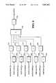
- RAID level 3One such array system described in the incorporated article, identified as a RAID level 3 system, comprises one or more groups of N+1 disks. Within each group, N disks are used to store data, and the additional disk is utilized to store parity information. During RAID level 3 write functions, each block of data is divided into N portions for storage among the N data disks. The corresponding parity information is written to a dedicated parity disk. When data is read, all N data disks must be accessed. The parity disk is used to reconstruct information in the event of a disk failure.
- a RAID level 3 system including five drivesis shown in FIG. 1. The disk drives are labeled DATA I through DATA 5. Data is striped across disks DATA 1 through DATA 4, each data disk receiving a portion of the data being saved. Parity information, generated through a bit-wise exclusive-OR of the data stored on drives DATA I through DATA 4, is saved on drive DATA 5.
- apparatusfor coupling a host bus associated with a host computer system with a plurality of array busses associated with an array of disk drives.
- the apparatusincludes a host register associated with each array bus, each host register being connected to the host bus for receiving data therefrom; a first array register associated with each array bus, each first array register being connected to a corresponding host register for receiving data therefrom and connected to its associated array bus for providing data thereto; and a second array register associated with each array bus, each second array register being connected to it associated array bus for receiving data therefrom and connected to the host bus for providing data thereto.
- the described embodimentincludes a state machine for coordinating the operation of the host and array registers to effect RAID level 3 read and write transfers between the host system and four array channels.
- the state machineincludes logic for generating, in response to a write request from the host system, a data strobe signal for effecting the transfer of data from the host bus into the host registers, a transfer strobe signal for effectuating the transfer of data from the host registers into corresponding first array registers, and an array strobe signal for bringing about the transfer of data from the first array registers onto their corresponding array busses.
- logic within the state machinegenerates strobe signals which are provided to the second array registers for effecting the transfer of data from the array busses into corresponding second array registers and the transfer of data from the second array registers onto the host bus.
- FIG. 1is a block diagram representation of a RAID level 3 array including four data,disk drives and one parity disk drive.
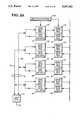
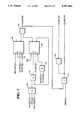
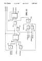
- FIGS. 2A and 2Billustrate a functional block diagram of a circuit for effecting bufferless data transfers between one host SCSI channel and an array of SCSI channels associated with a disk array in accordance with the present invention.
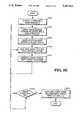
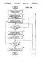
- FIGS. 3A and 3Billustrate a method for transferring data from a host device to a disk array in accordance with the present invention.
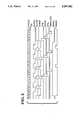
- FIG. 5is a time diagram for the write operation shown in the flow chart of FIGS. 3A and 3B.
- FIG. 7is a schematic diagram of a portion of the host state machine logic, shown in FIGS. 2A and 2B, for generating a host register strobe signal.
- FIG. 8is a schematic diagram of a portion of the host state machine logic for generating a host register full status signal.
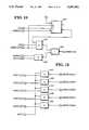
- FIG. 10is a schematic diagram of a portion of the array state machine logic for generating an array register strobe signal.
- FIG. 11is a schematic diagram of a portion of the host state machine logic for generating a data transfer strobe signal and an array register full signal.
- FIG. 12is a schematic diagram of a portion of the array state machine logic for generating individual array channel acknowledge signals.
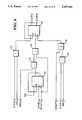
- FIGS. 2A and 2BA functional block diagram of a circuit for effecting bufferless data transfers between an eighteen-bit (sixteen data bits and two parity bits) host system data bus 12 and an array of nine-bit (eight data bits and one parity bit) disk drive busses 71 through 75 associated with a RAID level 3 disk array is illustrated in FIGS. 2A and 2B.
- the disk arraycomprises five disk drives, four of which store data and one for storing parity information.
- the circuitfunctions to hold data received from the host until the disk array is ready to accept the data and to convert the data from eighteen-bit bus 12 to nine-bit busses 71 through 74.
- the transfer circuit 70holds the data received from the disk array until the host system is ready to accept the data and converts the data from the nine-bit array busses to the eighteen-bit host bus.
- the circuitincludes a host SCSI adapter 14 to interface between the host system data bus 12 and two nine-bit SCSI data busses 16U and 16L.
- Four array data channelsare shown, each channel providing a data path from one of SCSI busses 16U or 16L to a corresponding one of disk drive busses 71 through 74.
- the first data channelincludes a host data register 21 connected to receive data from bus 16U, a first array data register 31 connected to receive the output of host data register 21, an array data latch 41 connected to receive the output of register 31, a data bus 51 connected to receive the output of latch 41, and a SCSI bus interface chip 61 linking SCSI bus 51 with array data bus 71.
- the remaining three data channelsare similarly constructed, connecting host busses 16U or 16L through respective host data registers 22 through 24, first array data registers 32 through 34, array latches 42 through 44, SCSI data busses 52 through 54, and SCSI bus interface chips 62 through 64 with disk drive busses 72 through 74.
- the first data channelincludes a second array data register 81 connected to receive data from bus 51 and a host data latch 91 connected between register 81 and bus 16U.
- Each of the remaining data channelsalso include a second array data register and a host data latch.
- the second array data registers for the second, third and fourths data channelsare identified by reference numerals 82 through 84, respectively.
- the host data latches for the second, third and fourths data channelsare identified by reference numerals 92 through 94, respectively.
- the operation of the data registers and host data latches described aboveis governed by a host state machine 100.
- An array state machine 200controls the operation of array data latches 41 through 44. State machines 100 and 200 are discussed in greater detail below.
- Parity circuit 47for generating parity information.
- Parity circuit 47includes connections to each of one of data busses 41 through 44 for receiving data therefrom and a connection through bus 55 and SCSI interface module 65 to disk drive bus 75 for providing parity information to the parity disk drive Parity circuit 47 generates parity information for RAID level 3 operations by performing a bit-wise exclusive-OR of the data received from data busses 41 through 44.
- the flow chart of FIGS. 3A and 3Billustrates a method for transferring data from SCSI interface 14 on the host side of the transfer circuit to any pair of disk drives (two data drives and one parity drive) or any two pairs of disk drives (four data drives and one parity drive) within the array.
- Data received from the hostis loaded into host data registers 21 through 24, transferred from the full host data registers into array data registers 31 through 34, and then provided to the disk array busses.
- the array state machinecombines the individual request signals issued by the array channels into a single array request signal (step W11), generates an acknowledgement (step W12), then waits until receipt of the array full status signal AFUL from the host state machine (step W13) to generate an array strobe signal to shift data from array registers 31 through 34 into latches 41 through 44 (step W14). Operation is then returned to step W7 which checks to determine if array registers 31 through 34 are full. If neither the array (step W7) or host (step W8) registers are full, the write procedure described above is repeated until the host terminates the write request.
- the host state machineDuring the above array state machine operations, the host state machine generates an acknowledge signal in response to the request issued by the host (step R10) then waits for the array register full signal generated during step R4 (step R I 1). As soon as the array registers are full, the host machine generates a data transfer signal to shift the data in the array registers into the host registers (steps R12 and R14) and a data strobe signal to shift data from the host registers to the host (steps R15 and R16). The read operation repeats until the array request is terminated (steps R7 and R8).
- the table belowlists and describes the signals received and generated by the host and array state machines for coordinating array read and write operations. An asterisk following a signal name indicates that the signal is active low.
- FIGS. 5 and 6illustrate the interrelationships between the above-identified signals for write and read operations, respectively. Several unique features are apparent from a review of the timing diagrams of FIGS. 5 and 6. For example:
- the host and array channelscan issue requests independently of the host register status and array registers status. This feature overlaps all the SCSI handshake overhead with other data access and transfer operations.
- the host and array requests acknowledge signalscan be extended to match any SCSI type interface, e.g., SCSI 1 or SCSI 2.
- the host requestis asynchronous to the array requests.
- the host and array state machinesuse the register banks to synchronize the requests without impacting the SCSI transfer rate. It should be noted that the data register statuses are modified asynchronous to the system clock, minimizing the access cycle of both state machines.
- the host state machinehas a cycle time (period of DSTRB* signal) less than or equal to five clock periods, which is less than the cycle time of any currently available SCSI chip. Each cycle effects the transfer of one data word.
- the array state machinehas a cycle time (period of ADACK* signal) less than or equal to five clock periods. Each cycle effecting the transfer of two data words.
- FIGS. 7 and 8are schematic diagrams of logic within the host state machine for generating host register strobe signal HS.STB* and host register full signal HFUL.
- the logic shown in FIG. 7generates signals DSTRB*, HS.STB and HS.STB* from a synchronous host request signal HS.REQS (a synchronized version of asynchronous host request signal HS.REQ), host register full signal HFUL, an acknowledge valid signal ACK.VALID, and a high-state signal identified as RAID3.
- HS.REQSa synchronized version of asynchronous host request signal HS.REQ
- ACK.VALIDacknowledge valid signal
- HFUL and HFUL*from transfer signals TX.STB and TX.STB*, direction signals DIR and DIR*, data strobe signal DSTRB*, high-state signal RAID3, and a host reset signal HS.RST*.
- Transfer strobe signals TX.STB and TX.STB* and array register full signals AFUL and AFUL*are determined from prior-state register full signals HFUL and AFUL, host reset signal HS.RST, prior-state transfer strobe signal TX.STB*, direction signal DIR and DIR* and array strobe signal ARRAY.STB.
- FIGS. 9, 10 and 12are schematic diagrams of logic contained within the array state machine for generating combined array request signal ADREQ, array register strobe signal ARRAY.STB and the individual array channel acknowledge signals, respectively.
- the logic of FIG. 9combines selected channel request signals ADREQ.CHAN1 through ADREQ.CHAN1 to generate the array request signal ADREQ.
- the channel request signals to combineare selected by setting corresponding enable signals PORT1.ACT through PORT5.ACT low.
- FIG. 10illustrates the state machine logic for generating array strobe signal ARRAY.STB.
- Signal ARRAY.STBis a function of signal DIR, a synchronized version of signal ADREQ, and an array interface read signal AIFREAD and array read strobe signal ARD.STB obtained by combining individual read and strobe signals from SCSI interface devices 61 through 65.
- a reset featureis provided with signal ADMARST.
- the logic shown in FIG. 12generates individual array channel acknowledge signals ADACK.CHAN1 through ADACK.CHAN5 form array acknowledge signal ADACK. Individual array channel signals are generated for those channels selected by setting corresponding enable signals PORT1.ACT through PORT5.ACT low.
- FIGS. 7 through 12The logic shown in FIGS. 7 through 12 is exemplary only and should be readily understood by one of ordinary skill in the art.
Landscapes
- Engineering & Computer Science (AREA)
- Theoretical Computer Science (AREA)
- Human Computer Interaction (AREA)
- Physics & Mathematics (AREA)
- General Engineering & Computer Science (AREA)
- General Physics & Mathematics (AREA)
- Bus Control (AREA)
Abstract
Description
______________________________________ SIGNAL DESCRIPTION ______________________________________ SYSCLK System clock DIR Data transfer direction. "1" write, "0" read HS.REQ Host request signal HS.STB* Host strobe signal DSTRB* Data strobe signal HFUL Host register full signal TX.STB Data transfer strobe signal AFUL Array register full signal ARRAY.STB Array strobe signal ADREQ Array request signal ADACK* Array acknowledge signal ______________________________________
Claims (12)
Priority Applications (1)
| Application Number | Priority Date | Filing Date | Title |
|---|---|---|---|
| US07/811,481US5287462A (en) | 1991-12-20 | 1991-12-20 | Bufferless SCSI to SCSI data transfer scheme for disk array applications |
Applications Claiming Priority (1)
| Application Number | Priority Date | Filing Date | Title |
|---|---|---|---|
| US07/811,481US5287462A (en) | 1991-12-20 | 1991-12-20 | Bufferless SCSI to SCSI data transfer scheme for disk array applications |
Publications (1)
| Publication Number | Publication Date |
|---|---|
| US5287462Atrue US5287462A (en) | 1994-02-15 |
Family
ID=25206666
Family Applications (1)
| Application Number | Title | Priority Date | Filing Date |
|---|---|---|---|
| US07/811,481Expired - LifetimeUS5287462A (en) | 1991-12-20 | 1991-12-20 | Bufferless SCSI to SCSI data transfer scheme for disk array applications |
Country Status (1)
| Country | Link |
|---|---|
| US (1) | US5287462A (en) |
Cited By (37)
| Publication number | Priority date | Publication date | Assignee | Title |
|---|---|---|---|---|
| US5392244A (en)* | 1993-08-19 | 1995-02-21 | Hewlett-Packard Company | Memory systems with data storage redundancy management |
| US5463776A (en)* | 1994-09-22 | 1995-10-31 | Hewlett-Packard Company | Storage management system for concurrent generation and fair allocation of disk space among competing requests |
| US5537534A (en)* | 1995-02-10 | 1996-07-16 | Hewlett-Packard Company | Disk array having redundant storage and methods for incrementally generating redundancy as data is written to the disk array |
| US5542065A (en)* | 1995-02-10 | 1996-07-30 | Hewlett-Packard Company | Methods for using non-contiguously reserved storage space for data migration in a redundant hierarchic data storage system |
| US5548712A (en)* | 1995-01-19 | 1996-08-20 | Hewlett-Packard Company | Data storage system and method for managing asynchronous attachment and detachment of storage disks |
| US5553230A (en)* | 1995-01-18 | 1996-09-03 | Hewlett-Packard Company | Identifying controller pairs in a dual controller disk array |
| US5553238A (en)* | 1995-01-19 | 1996-09-03 | Hewlett-Packard Company | Powerfail durable NVRAM testing |
| US5568641A (en)* | 1995-01-18 | 1996-10-22 | Hewlett-Packard Company | Powerfail durable flash EEPROM upgrade |
| US5572661A (en)* | 1994-10-05 | 1996-11-05 | Hewlett-Packard Company | Methods and system for detecting data loss in a hierarchic data storage system |
| US5574863A (en)* | 1994-10-25 | 1996-11-12 | Hewlett-Packard Company | System for using mirrored memory as a robust communication path between dual disk storage controllers |
| US5596710A (en)* | 1994-10-25 | 1997-01-21 | Hewlett-Packard Company | Method for managing roll forward and roll back logs of a transaction object |
| US5604902A (en)* | 1995-02-16 | 1997-02-18 | Hewlett-Packard Company | Hole plugging garbage collection for a data storage system |
| US5615352A (en)* | 1994-10-05 | 1997-03-25 | Hewlett-Packard Company | Methods for adding storage disks to a hierarchic disk array while maintaining data availability |
| US5623598A (en)* | 1994-11-22 | 1997-04-22 | Hewlett-Packard Company | Method for identifying ways to improve performance in computer data storage systems |
| US5644789A (en)* | 1995-01-19 | 1997-07-01 | Hewlett-Packard Company | System and method for handling I/O requests over an interface bus to a storage disk array |
| US5651133A (en)* | 1995-02-01 | 1997-07-22 | Hewlett-Packard Company | Methods for avoiding over-commitment of virtual capacity in a redundant hierarchic data storage system |
| US5659704A (en)* | 1994-12-02 | 1997-08-19 | Hewlett-Packard Company | Methods and system for reserving storage space for data migration in a redundant hierarchic data storage system by dynamically computing maximum storage space for mirror redundancy |
| US5664187A (en)* | 1994-10-26 | 1997-09-02 | Hewlett-Packard Company | Method and system for selecting data for migration in a hierarchic data storage system using frequency distribution tables |
| US5666512A (en)* | 1995-02-10 | 1997-09-09 | Hewlett-Packard Company | Disk array having hot spare resources and methods for using hot spare resources to store user data |
| US5668971A (en)* | 1992-12-01 | 1997-09-16 | Compaq Computer Corporation | Posted disk read operations performed by signalling a disk read complete to the system prior to completion of data transfer |
| US5696934A (en)* | 1994-06-22 | 1997-12-09 | Hewlett-Packard Company | Method of utilizing storage disks of differing capacity in a single storage volume in a hierarchial disk array |
| US5699510A (en)* | 1994-12-15 | 1997-12-16 | Hewlett-Packard Company | Failure detection system for a mirrored memory dual controller disk storage system |
| US5701514A (en)* | 1994-04-01 | 1997-12-23 | International Business Machines Corporation | System providing user definable selection of different data transmission modes of drivers of an I/O controller transmitting to peripherals with different data transmission rate |
| US5819310A (en)* | 1996-05-24 | 1998-10-06 | Emc Corporation | Method and apparatus for reading data from mirrored logical volumes on physical disk drives |
| US5822330A (en)* | 1996-04-19 | 1998-10-13 | International Business Machines Corp. | Method and system for dynamically adjusting signal skewing |
| US5835694A (en)* | 1996-12-06 | 1998-11-10 | International Business Machines Corporation | Raid-configured disk drive array wherein array control occurs at the disk drive level |
| US5838891A (en)* | 1995-03-22 | 1998-11-17 | Mitsubishi Denki Kabushiki Kaisha | Data storage system and storage managing method |
| US5893138A (en)* | 1995-10-02 | 1999-04-06 | International Business Machines Corporation | System and method for improving channel hardware performance for an array controller |
| US5928367A (en)* | 1995-01-06 | 1999-07-27 | Hewlett-Packard Company | Mirrored memory dual controller disk storage system |
| US6055577A (en)* | 1996-05-06 | 2000-04-25 | Oracle Corporation | System for granting bandwidth for real time processes and assigning bandwidth for non-real time processes while being forced to periodically re-arbitrate for new assigned bandwidth |
| US6108812A (en)* | 1996-06-20 | 2000-08-22 | Lsi Logic Corporation | Target device XOR engine |
| CN1060872C (en)* | 1996-05-03 | 2001-01-17 | 华中理工大学 | Disc matrix system integrating method |
| US6654853B1 (en) | 1996-12-23 | 2003-11-25 | Lsi Logic Corporation | Method of secondary to secondary data transfer with mirroring |
| US6671751B1 (en)* | 2000-04-07 | 2003-12-30 | Key Technology Corporation | Raid device for establishing a direct passage between a host computer and a hard disk by a data hub selectively passing only data to be accessed |
| US6708285B2 (en) | 2001-03-15 | 2004-03-16 | Hewlett-Packard Development Company, L.P. | Redundant controller data storage system having system and method for handling controller resets |
| US6715101B2 (en) | 2001-03-15 | 2004-03-30 | Hewlett-Packard Development Company, L.P. | Redundant controller data storage system having an on-line controller removal system and method |
| US6802023B2 (en) | 2001-03-15 | 2004-10-05 | Hewlett-Packard Development Company, L.P. | Redundant controller data storage system having hot insertion system and method |
Citations (11)
| Publication number | Priority date | Publication date | Assignee | Title |
|---|---|---|---|---|
| US4716525A (en)* | 1985-04-15 | 1987-12-29 | Concurrent Computer Corporation | Peripheral controller for coupling data buses having different protocol and transfer rates |
| US4722085A (en)* | 1986-02-03 | 1988-01-26 | Unisys Corp. | High capacity disk storage system having unusually high fault tolerance level and bandpass |
| US4864532A (en)* | 1987-09-21 | 1989-09-05 | Unisys Corporation | Small computer systems interface--data link processor |
| US4914656A (en)* | 1988-06-28 | 1990-04-03 | Storage Technology Corporation | Disk drive memory |
| US5077736A (en)* | 1988-06-28 | 1991-12-31 | Storage Technology Corporation | Disk drive memory |
| US5088081A (en)* | 1990-03-28 | 1992-02-11 | Prime Computer, Inc. | Method and apparatus for improved disk access |
| US5128810A (en)* | 1988-08-02 | 1992-07-07 | Cray Research, Inc. | Single disk emulation interface for an array of synchronous spindle disk drives |
| US5146588A (en)* | 1990-11-26 | 1992-09-08 | Storage Technology Corporation | Redundancy accumulator for disk drive array memory |
| US5148432A (en)* | 1988-11-14 | 1992-09-15 | Array Technology Corporation | Arrayed disk drive system and method |
| US5191584A (en)* | 1991-02-20 | 1993-03-02 | Micropolis Corporation | Mass storage array with efficient parity calculation |
| US5206943A (en)* | 1989-11-03 | 1993-04-27 | Compaq Computer Corporation | Disk array controller with parity capabilities |
- 1991
- 1991-12-20USUS07/811,481patent/US5287462A/ennot_activeExpired - Lifetime
Patent Citations (11)
| Publication number | Priority date | Publication date | Assignee | Title |
|---|---|---|---|---|
| US4716525A (en)* | 1985-04-15 | 1987-12-29 | Concurrent Computer Corporation | Peripheral controller for coupling data buses having different protocol and transfer rates |
| US4722085A (en)* | 1986-02-03 | 1988-01-26 | Unisys Corp. | High capacity disk storage system having unusually high fault tolerance level and bandpass |
| US4864532A (en)* | 1987-09-21 | 1989-09-05 | Unisys Corporation | Small computer systems interface--data link processor |
| US4914656A (en)* | 1988-06-28 | 1990-04-03 | Storage Technology Corporation | Disk drive memory |
| US5077736A (en)* | 1988-06-28 | 1991-12-31 | Storage Technology Corporation | Disk drive memory |
| US5128810A (en)* | 1988-08-02 | 1992-07-07 | Cray Research, Inc. | Single disk emulation interface for an array of synchronous spindle disk drives |
| US5148432A (en)* | 1988-11-14 | 1992-09-15 | Array Technology Corporation | Arrayed disk drive system and method |
| US5206943A (en)* | 1989-11-03 | 1993-04-27 | Compaq Computer Corporation | Disk array controller with parity capabilities |
| US5088081A (en)* | 1990-03-28 | 1992-02-11 | Prime Computer, Inc. | Method and apparatus for improved disk access |
| US5146588A (en)* | 1990-11-26 | 1992-09-08 | Storage Technology Corporation | Redundancy accumulator for disk drive array memory |
| US5191584A (en)* | 1991-02-20 | 1993-03-02 | Micropolis Corporation | Mass storage array with efficient parity calculation |
Non-Patent Citations (1)
| Title |
|---|
| A Case For Redundant Arrays of Inexpensive Disks (Raid) by David A. Patterson, et al., Computer Science Division (EECS) University of California, Report No. UCB/CSD 87/391, Dec. 1987.* |
Cited By (39)
| Publication number | Priority date | Publication date | Assignee | Title |
|---|---|---|---|---|
| US5668971A (en)* | 1992-12-01 | 1997-09-16 | Compaq Computer Corporation | Posted disk read operations performed by signalling a disk read complete to the system prior to completion of data transfer |
| US5392244A (en)* | 1993-08-19 | 1995-02-21 | Hewlett-Packard Company | Memory systems with data storage redundancy management |
| US5701514A (en)* | 1994-04-01 | 1997-12-23 | International Business Machines Corporation | System providing user definable selection of different data transmission modes of drivers of an I/O controller transmitting to peripherals with different data transmission rate |
| US5696934A (en)* | 1994-06-22 | 1997-12-09 | Hewlett-Packard Company | Method of utilizing storage disks of differing capacity in a single storage volume in a hierarchial disk array |
| US5463776A (en)* | 1994-09-22 | 1995-10-31 | Hewlett-Packard Company | Storage management system for concurrent generation and fair allocation of disk space among competing requests |
| US5572661A (en)* | 1994-10-05 | 1996-11-05 | Hewlett-Packard Company | Methods and system for detecting data loss in a hierarchic data storage system |
| US5615352A (en)* | 1994-10-05 | 1997-03-25 | Hewlett-Packard Company | Methods for adding storage disks to a hierarchic disk array while maintaining data availability |
| US5574863A (en)* | 1994-10-25 | 1996-11-12 | Hewlett-Packard Company | System for using mirrored memory as a robust communication path between dual disk storage controllers |
| US5596710A (en)* | 1994-10-25 | 1997-01-21 | Hewlett-Packard Company | Method for managing roll forward and roll back logs of a transaction object |
| US5664187A (en)* | 1994-10-26 | 1997-09-02 | Hewlett-Packard Company | Method and system for selecting data for migration in a hierarchic data storage system using frequency distribution tables |
| US5623598A (en)* | 1994-11-22 | 1997-04-22 | Hewlett-Packard Company | Method for identifying ways to improve performance in computer data storage systems |
| US5659704A (en)* | 1994-12-02 | 1997-08-19 | Hewlett-Packard Company | Methods and system for reserving storage space for data migration in a redundant hierarchic data storage system by dynamically computing maximum storage space for mirror redundancy |
| US5699510A (en)* | 1994-12-15 | 1997-12-16 | Hewlett-Packard Company | Failure detection system for a mirrored memory dual controller disk storage system |
| US5928367A (en)* | 1995-01-06 | 1999-07-27 | Hewlett-Packard Company | Mirrored memory dual controller disk storage system |
| US5553230A (en)* | 1995-01-18 | 1996-09-03 | Hewlett-Packard Company | Identifying controller pairs in a dual controller disk array |
| US5568641A (en)* | 1995-01-18 | 1996-10-22 | Hewlett-Packard Company | Powerfail durable flash EEPROM upgrade |
| US5644789A (en)* | 1995-01-19 | 1997-07-01 | Hewlett-Packard Company | System and method for handling I/O requests over an interface bus to a storage disk array |
| US5553238A (en)* | 1995-01-19 | 1996-09-03 | Hewlett-Packard Company | Powerfail durable NVRAM testing |
| US5548712A (en)* | 1995-01-19 | 1996-08-20 | Hewlett-Packard Company | Data storage system and method for managing asynchronous attachment and detachment of storage disks |
| US5729679A (en)* | 1995-01-19 | 1998-03-17 | Hewlett-Packard Company | Powerfail durable NVRAM testing |
| US5651133A (en)* | 1995-02-01 | 1997-07-22 | Hewlett-Packard Company | Methods for avoiding over-commitment of virtual capacity in a redundant hierarchic data storage system |
| US5666512A (en)* | 1995-02-10 | 1997-09-09 | Hewlett-Packard Company | Disk array having hot spare resources and methods for using hot spare resources to store user data |
| US5542065A (en)* | 1995-02-10 | 1996-07-30 | Hewlett-Packard Company | Methods for using non-contiguously reserved storage space for data migration in a redundant hierarchic data storage system |
| US5537534A (en)* | 1995-02-10 | 1996-07-16 | Hewlett-Packard Company | Disk array having redundant storage and methods for incrementally generating redundancy as data is written to the disk array |
| US5604902A (en)* | 1995-02-16 | 1997-02-18 | Hewlett-Packard Company | Hole plugging garbage collection for a data storage system |
| US5838891A (en)* | 1995-03-22 | 1998-11-17 | Mitsubishi Denki Kabushiki Kaisha | Data storage system and storage managing method |
| US5893138A (en)* | 1995-10-02 | 1999-04-06 | International Business Machines Corporation | System and method for improving channel hardware performance for an array controller |
| US5822330A (en)* | 1996-04-19 | 1998-10-13 | International Business Machines Corp. | Method and system for dynamically adjusting signal skewing |
| CN1060872C (en)* | 1996-05-03 | 2001-01-17 | 华中理工大学 | Disc matrix system integrating method |
| US6055577A (en)* | 1996-05-06 | 2000-04-25 | Oracle Corporation | System for granting bandwidth for real time processes and assigning bandwidth for non-real time processes while being forced to periodically re-arbitrate for new assigned bandwidth |
| US5819310A (en)* | 1996-05-24 | 1998-10-06 | Emc Corporation | Method and apparatus for reading data from mirrored logical volumes on physical disk drives |
| US5987566A (en)* | 1996-05-24 | 1999-11-16 | Emc Corporation | Redundant storage with mirroring by logical volume with diverse reading process |
| US6108812A (en)* | 1996-06-20 | 2000-08-22 | Lsi Logic Corporation | Target device XOR engine |
| US5835694A (en)* | 1996-12-06 | 1998-11-10 | International Business Machines Corporation | Raid-configured disk drive array wherein array control occurs at the disk drive level |
| US6654853B1 (en) | 1996-12-23 | 2003-11-25 | Lsi Logic Corporation | Method of secondary to secondary data transfer with mirroring |
| US6671751B1 (en)* | 2000-04-07 | 2003-12-30 | Key Technology Corporation | Raid device for establishing a direct passage between a host computer and a hard disk by a data hub selectively passing only data to be accessed |
| US6708285B2 (en) | 2001-03-15 | 2004-03-16 | Hewlett-Packard Development Company, L.P. | Redundant controller data storage system having system and method for handling controller resets |
| US6715101B2 (en) | 2001-03-15 | 2004-03-30 | Hewlett-Packard Development Company, L.P. | Redundant controller data storage system having an on-line controller removal system and method |
| US6802023B2 (en) | 2001-03-15 | 2004-10-05 | Hewlett-Packard Development Company, L.P. | Redundant controller data storage system having hot insertion system and method |
Similar Documents
| Publication | Publication Date | Title |
|---|---|---|
| US5287462A (en) | Bufferless SCSI to SCSI data transfer scheme for disk array applications | |
| US5257391A (en) | Disk controller having host interface and bus switches for selecting buffer and drive busses respectively based on configuration control signals | |
| EP0572564B1 (en) | Parity calculation in an efficient array of mass storage devices | |
| US6237052B1 (en) | On-the-fly redundancy operation for forming redundant drive data and reconstructing missing data as data transferred between buffer memory and disk drives during write and read operation respectively | |
| JP3237736B2 (en) | Matrix structure of data storage device | |
| US5418925A (en) | Fast write I/O handling in a disk array using spare drive for buffering | |
| US5388108A (en) | Delayed initiation of read-modify-write parity operations in a raid level 5 disk array | |
| US5883909A (en) | Method and apparatus for reducing data transfers across a memory bus of a disk array controller | |
| EP0550853B1 (en) | Array of disk drives with redundant channels | |
| US5596708A (en) | Method and apparatus for the protection of write data in a disk array | |
| JP3181398B2 (en) | Array type recording device | |
| EP0508604B1 (en) | Disk array controller for data storage system | |
| US5146588A (en) | Redundancy accumulator for disk drive array memory | |
| CA2087162A1 (en) | High-speed, high-capacity, fault-tolerant, error-correcting storage system for binary computers | |
| US5471640A (en) | Programmable disk array controller having n counters for n disk drives for stripping data where each counter addresses specific memory location by a count n | |
| JPH10111767A (en) | Mass storage device | |
| US6678768B1 (en) | Method and apparatus for configuring redundant array of independent disks (RAID) | |
| US5862313A (en) | Raid system using I/O buffer segment to temporary store striped and parity data and connecting all disk drives via a single time multiplexed network | |
| JPH10301720A (en) | Disk array device | |
| US5964895A (en) | VRAM-based parity engine for use in disk array controller | |
| US5375217A (en) | Method and apparatus for synchronizing disk drive requests within a disk array | |
| US6418508B1 (en) | Information storage controller for controlling the reading/writing of information to and from a plurality of magnetic disks and an external device | |
| KR100419396B1 (en) | Disk array device and its implementation method | |
| JP4444636B2 (en) | Disk subsystem | |
| JP2814734B2 (en) | Magnetic disk drive |
Legal Events
| Date | Code | Title | Description |
|---|---|---|---|
| AS | Assignment | Owner name:NCR CORPORATION A CORPORATION OF MARYLAND Free format text:ASSIGNMENT OF ASSIGNORS INTEREST.;ASSIGNORS:JIBBE, MAHMOUD K.;MCCOMBS, CRAIG C.;REEL/FRAME:005969/0997 Effective date:19911216 Owner name:NCR CORPORATION, OHIO Free format text:ASSIGNMENT OF ASSIGNORS INTEREST;ASSIGNORS:JIBBE, MAHMOUD K.;MCCOMBS, CRAIG C.;REEL/FRAME:005969/0997 Effective date:19911216 | |
| STCF | Information on status: patent grant | Free format text:PATENTED CASE | |
| CC | Certificate of correction | ||
| AS | Assignment | Owner name:HYUNDAI ELECTRONICS AMERICA Free format text:ASSIGNMENT OF ASSIGNORS INTEREST;ASSIGNOR:AT&T GLOBAL INFORMATION SOLUTIONS COMPANY (FORMERLY KNOWN AS NCR CORPORATION);REEL/FRAME:007408/0104 Effective date:19950215 | |
| AS | Assignment | Owner name:SYMBIOS LOGIC INC., COLORADO Free format text:ASSIGNMENT OF ASSIGNORS INTEREST;ASSIGNOR:HYUNDAI ELECTRONICS AMERICA;REEL/FRAME:007629/0431 Effective date:19950818 | |
| FPAY | Fee payment | Year of fee payment:4 | |
| AS | Assignment | Owner name:SYMBIOS, INC ., COLORADO Free format text:CHANGE OF NAME;ASSIGNOR:SYMBIOS LOGIC INC.;REEL/FRAME:009089/0936 Effective date:19971210 | |
| AS | Assignment | Owner name:LEHMAN COMMERCIAL PAPER INC., AS ADMINISTRATIVE AG Free format text:SECURITY AGREEMENT;ASSIGNORS:HYUNDAI ELECTRONICS AMERICA, A CORP. OF CALIFORNIA;SYMBIOS, INC., A CORP. OF DELAWARE;REEL/FRAME:009396/0441 Effective date:19980226 | |
| AS | Assignment | Owner name:HYUNDAI ELECTRONICS AMERICA, CALIFORNIA Free format text:TERMINATION AND LICENSE AGREEMENT;ASSIGNOR:SYMBIOS, INC.;REEL/FRAME:009596/0539 Effective date:19980806 | |
| REMI | Maintenance fee reminder mailed | ||
| FPAY | Fee payment | Year of fee payment:8 | |
| SULP | Surcharge for late payment | Year of fee payment:7 | |
| AS | Assignment | Owner name:HYNIX SEMICONDUCTOR AMERICA INC., CALIFORNIA Free format text:CHANGE OF NAME;ASSIGNOR:HYUNDAI ELECTRONICS AMERICA;REEL/FRAME:015246/0599 Effective date:20010412 Owner name:HYNIX SEMICONDUCTOR INC., KOREA, REPUBLIC OF Free format text:ASSIGNMENT OF ASSIGNORS INTEREST;ASSIGNOR:HYNIX SEMICONDUCTOR AMERICA, INC.;REEL/FRAME:015279/0556 Effective date:20040920 | |
| AS | Assignment | Owner name:MAGNACHIP SEMICONDUCTOR, LTD., KOREA, REPUBLIC OF Free format text:ASSIGNMENT OF ASSIGNORS INTEREST;ASSIGNOR:HYNIX SEMICONDUCTOR, INC.;REEL/FRAME:016216/0649 Effective date:20041004 | |
| AS | Assignment | Owner name:U.S. BANK NATIONAL ASSOCIATION, AS COLLATERAL TRUS Free format text:SECURITY INTEREST;ASSIGNOR:MAGNACHIP SEMICONDUCTOR, LTD.;REEL/FRAME:016470/0530 Effective date:20041223 | |
| AS | Assignment | Owner name:SYMBIOS, INC., COLORADO Free format text:RELEASE OF SECURITY INTEREST;ASSIGNOR:LEHMAN COMMERICAL PAPER INC.;REEL/FRAME:016602/0895 Effective date:20050107 Owner name:HYUNDAI ELECTRONICS AMERICA, CALIFORNIA Free format text:RELEASE OF SECURITY INTEREST;ASSIGNOR:LEHMAN COMMERICAL PAPER INC.;REEL/FRAME:016602/0895 Effective date:20050107 | |
| FPAY | Fee payment | Year of fee payment:12 | |
| AS | Assignment | Owner name:TAIWAN SEMICONDUCTOR MANUFACTURING CO., LTD., TAIW Free format text:ASSIGNMENT OF ASSIGNORS INTEREST;ASSIGNORS:NCR CORPORATION;MAGNACHIP SEMICONDUCTOR, LTD.;REEL/FRAME:021398/0702;SIGNING DATES FROM 20071114 TO 20071115 |