US5287238A - Dual spin valve magnetoresistive sensor - Google Patents
Dual spin valve magnetoresistive sensorDownload PDFInfo
- Publication number
- US5287238A US5287238AUS07/973,106US97310692AUS5287238AUS 5287238 AUS5287238 AUS 5287238AUS 97310692 AUS97310692 AUS 97310692AUS 5287238 AUS5287238 AUS 5287238A
- Authority
- US
- United States
- Prior art keywords
- layer
- layers
- ferromagnetic material
- magnetoresistive sensor
- magnetic
- Prior art date
- Legal status (The legal status is an assumption and is not a legal conclusion. Google has not performed a legal analysis and makes no representation as to the accuracy of the status listed.)
- Expired - Lifetime
Links
Images


Classifications
- B—PERFORMING OPERATIONS; TRANSPORTING
- B82—NANOTECHNOLOGY
- B82Y—SPECIFIC USES OR APPLICATIONS OF NANOSTRUCTURES; MEASUREMENT OR ANALYSIS OF NANOSTRUCTURES; MANUFACTURE OR TREATMENT OF NANOSTRUCTURES
- B82Y25/00—Nanomagnetism, e.g. magnetoimpedance, anisotropic magnetoresistance, giant magnetoresistance or tunneling magnetoresistance
- G—PHYSICS
- G11—INFORMATION STORAGE
- G11B—INFORMATION STORAGE BASED ON RELATIVE MOVEMENT BETWEEN RECORD CARRIER AND TRANSDUCER
- G11B5/00—Recording by magnetisation or demagnetisation of a record carrier; Reproducing by magnetic means; Record carriers therefor
- G11B5/127—Structure or manufacture of heads, e.g. inductive
- G11B5/33—Structure or manufacture of flux-sensitive heads, i.e. for reproduction only; Combination of such heads with means for recording or erasing only
- G11B5/39—Structure or manufacture of flux-sensitive heads, i.e. for reproduction only; Combination of such heads with means for recording or erasing only using magneto-resistive devices or effects
- G11B5/3903—Structure or manufacture of flux-sensitive heads, i.e. for reproduction only; Combination of such heads with means for recording or erasing only using magneto-resistive devices or effects using magnetic thin film layers or their effects, the films being part of integrated structures
- B—PERFORMING OPERATIONS; TRANSPORTING
- B82—NANOTECHNOLOGY
- B82Y—SPECIFIC USES OR APPLICATIONS OF NANOSTRUCTURES; MEASUREMENT OR ANALYSIS OF NANOSTRUCTURES; MANUFACTURE OR TREATMENT OF NANOSTRUCTURES
- B82Y10/00—Nanotechnology for information processing, storage or transmission, e.g. quantum computing or single electron logic
- G—PHYSICS
- G11—INFORMATION STORAGE
- G11B—INFORMATION STORAGE BASED ON RELATIVE MOVEMENT BETWEEN RECORD CARRIER AND TRANSDUCER
- G11B5/00—Recording by magnetisation or demagnetisation of a record carrier; Reproducing by magnetic means; Record carriers therefor
- G11B5/127—Structure or manufacture of heads, e.g. inductive
- G11B5/33—Structure or manufacture of flux-sensitive heads, i.e. for reproduction only; Combination of such heads with means for recording or erasing only
- G11B5/39—Structure or manufacture of flux-sensitive heads, i.e. for reproduction only; Combination of such heads with means for recording or erasing only using magneto-resistive devices or effects
- G11B2005/3996—Structure or manufacture of flux-sensitive heads, i.e. for reproduction only; Combination of such heads with means for recording or erasing only using magneto-resistive devices or effects large or giant magnetoresistive effects [GMR], e.g. as generated in spin-valve [SV] devices
Definitions
- the present inventionrelates generally to magnetic sensors for reading information signals recorded in a magnetic medium and, more particularly, to an improved magnetoresistive read sensor which utilizes a multilayered, dual spin valve structure and antiferromagnetic exchange coupling to provide a fixed bias field for the sensor.
- the prior artdiscloses a magnetic read transducer referred to as a magnetoresistive (MR) sensor or head which has been shown to be capable of reading data from a magnetic surface at great linear densities.
- An MR sensordetects magnetic field signals through the resistance changes of a read element fabricated of a magnetic material as a function of the strength and direction of magnetic flux being sensed by the read element.
- These prior art MR sensorsoperate on the basis of the anisotropic magnetoresistive (AMR) effect in which a component of the read element resistance varies as the square of the cosine (cos 2 ) of the angle between the magnetization and the direction of sense current flow through the element.
- AMRanisotropic magnetoresistive
- U.S. Pat. No. 4,949,039 to Grunbergdescribes a layered magnetic structure which yields enhanced MR effects caused by antiparallel alignment of the magnetizations in the magnetic layers.
- Grunberglists ferromagnetic transition metals and alloys, but does not indicate preferred materials from the list for superior MR signal amplitude.
- Grunbergfurther describes the use of antiferromagnetic-type exchange coupling to obtain the antiparallel alignment in which adjacent layers of ferromagnetic materials are separated by a thin interlayer of chromium (Cr) or yttrium (Y).
- U.S. Pat. No. 5,206,590assigned to the instant assignee, discloses an MR sensor in which the resistance between two uncoupled ferromagnetic layers is observed to vary as the cosine of the angle between the magnetizations of the two layers and which is independent of the direction of current flow through the sensor.
- This mechanismproduces a magnetoresistance that, for selected combinations of materials, is greater in magnitude than the AMR, and is referred to as giant magnetoresistance or the "spin valve" (SV) magnetoresistance.
- SVspin valve
- a magnetoresistive (MR) read sensor having a multilayered, dual spin valve structureprovides a large MR response at low applied magnetic fields.
- the MR structurecomprises a layered structure formed on a suitable substrate including first, second and third thin film layers of ferromagnetic material separated by thin film layers of non-magnetic metallic material.
- the first and third layers of ferromagnetic materiali.e., the outer layers of the structure, have their magnetization orientation fixed while the second, intermediate layer of ferromagnetic material is magnetically soft and has its magnetization oriented substantially perpendicular to that of both the outer layers of ferromagnetic material.
- the magnetization directions of the first and third layers of ferromagnetic materialcan be fixed or "pinned" by any of several methods including hard biasing or exchange biasing by an adjacent antiferromagnetic layer as is known in the art.
- the two outer ferromagnetic layershave their magnetization directions pinned antiparallel to each other and, thus, each pinned layer acts as a magnetic flux keeper for the other pinned layer.
- the magnetization direction of the second, intermediate ferromagnetic layeris free to rotate with an applied magnetic field.
- the electrical resistance of each pair of ferromagnetic layers, i.e., the first and second layers and the second and third layers,varies as a function of the cosine of the angle between the magnetization directions of the two ferromagnetic layers of the pair.
- an MR sensorcan be fabricated in which the resistance of the sensor varies from a minimum to a maximum value when the magnetization direction of the intermediate, free layer rotates from a direction near parallel to the magnetization of the first, outer pinned layer, for example, to a direction near parallel to the magnetization direction of the third, outer pinned layer.
- a current sourceprovides a sense current to the MR sensor which generates a voltage drop across the read element proportional to the variations in the resistance of the MR sensor due to the rotation of the magnetization in the intermediate, free layer of ferromagnetic material as a function of the applied external magnetic field being sensed.
- a multilayered, dual spin valve sensorin which the magnetization directions in the two outer ferromagnetic layers are parallel with both being perpendicular to the direction of magnetization in the center, free ferromagnetic layer.
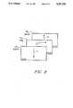
- FIG. 1is a simplified block diagram of a magnetic disk storage system embodying the present invention
- FIG. 2is an exploded view in perspective of a preferred embodiment of the magnetoresistive sensor according to the principles of the present invention
- FIG. 3is an end view of another preferred embodiment of the magnetoresistive sensor according to the principles of the present invention.
- FIG. 4is a is a graph illustrating the hysteresis loop and the magnetoresistive response for a prior art spin valve MR sensor structure
- FIG. 5is a graph illustrating the magnetoresistive response for the MR sensor shown in FIG. 2;
- FIGS. 6(a) and 6(b)are schematic diagrams illustrating a spin valve structure having positive giant magnetoresistance
- FIGS. 7(a) and 7(b)are schematic diagrams illustrating a spin valve structure having negative giant magnetoresistance
- FIG. 8is a schematic diagram of a dual spin valve utilizing positive and negative giant magnetoresistance according to the principles of the present invention.
- FIG. 9is an exploded view in perspective of another preferred embodiment of the magnetoresistive sensor according to the principles of the present invention.
- FIG. 10is an end view of another embodiment of a magnetoresistive sensor constructed in accordance with the present invention.
- At least one rotatable magnetic disk 12is supported on a spindle 14 and rotated by a disk drive motor 18.
- the magnetic recording media on each diskis in the form of an annular pattern of concentric data tracks (not shown) on disk 12.
- At least one slider 13is positioned on the disk 12, each slider 13 supporting one or more magnetic read/write transducers 21, typically referred to as read/write heads. As the disks rotate, the sliders 13 are moved radially in and out over the disk surface 22 so that the heads 21 may access different portions of the disk where desired data is recorded.
- Each slider 13is attached to an actuator arm 19 by means of a suspension 15.
- the suspension 15provides a slight spring force which biases the slider 13 against the disk surface 22.
- Each actuator arm 19is attached to an actuator means 27.
- the actuator means as shown in FIG. 1may be a voice coil motor (VCM), for example.
- VCMcomprises a coil moveable within a fixed magnetic field, the direction and velocity of the coil movements being controlled by the motor current signals supplied by a controller.
- the rotation of the disk 12generates an air bearing between the slider 13 and the disk surface 22 which exerts an upward force or lift on the slider.
- the air bearingthus counterbalances the slight spring force of the suspension 15 and supports the slider 13 off and slightly above the disk surface by a small, substantially constant spacing during operation.
- control unit 29The various components of the disk storage system are controlled in operation by control signals generated by control unit 29, such as access control signals and internal clock signals.
- control unit 29comprises logic control circuits, storage means and a microprocessor, for example.
- the control unit 29generates control signals to control various system operations such as drive motor control signals on line 23 and head position and seek control signals on line 28.
- the control signals on line 28provide the desired current profiles to optimally move and position a selected slider 13 to the desired data track on the associated disk 12.
- Read and write signalsare communicated to and from read/write heads 21 by means of recording channel 25.
- disk storage systemsmay contain a large number of disks and actuators, and each actuator may support a number of sliders.
- a preferred embodiment of an MR sensor 30comprises a first thin film layer 31 of ferromagnetic material, a first thin film layer 33 of a non-magnetic metallic material, a second thin film layer of ferromagnetic material 35, a second thin film layer 37 of a non-magnetic metallic material and a third thin film layer 39 of ferromagnetic material.
- the magnetizations of the two outer layers 31 and 39 of ferromagnetic materialare oriented parallel to each other, i.e., in the same direction, and at an angle of about 90 degrees with respect to the magnetization of the intermediate layer 35 of ferromagnetic material in the absence of an externally applied magnetic field as indicated by arrows 32, 34 and 38, respectively.
- the magnetization directions of the first and third outer layers, 31 and 39 of ferromagnetic materialare fixed or pinned in a preferred orientation as shown by the arrows 32 and 38.
- the magnetization in the intermediate layer 35 of ferromagnetic materialis free to rotate its direction in response to an externally applied magnetic field (such as magnetic field h as shown in FIG. 2), as shown by the dashed arrows 34 on layer 35 in FIG. 2.
- an externally applied magnetic fieldsuch as magnetic field h as shown in FIG. 2
- the ferromagnetic layers 31, 35 and 39can be fabricated of any suitable magnetic material such as cobalt (Co), iron (Fe), nickel (Ni) and their alloys such as nickel-iron (NiFe), nickel-cobalt (NiCo) and iron-cobalt (FeCo), for example.
- the non-magnetic metallic spacer layers 33 and 37comprise copper (Cu), for example, or other suitable noble metal such as silver (Ag) or gold (Au) or their alloys.
- the fixed or pinned outer ferromagnetic layers 31 and 39can be exchange biased by adjacent layers (as shown in FIG. 9) of an antiferromagnetic material such as iron-manganese (FeMn), for example.
- an MR sensor based on the spin valve effect wherein a pinned ferromagnetic layer is exchanged biased by an adjacent antiferromagnetic layeris described in greater detail in the above referenced patent application Ser. No. 07/937,620 hereby incorporated by reference as if fully set forth herein.
- the magnetization directions of the pinned ferromagnetic layers 31, 39can be fixed by use of an adjacent hard magnetic layer or by use of a material having a sufficiently high coercivity for the outer pinned layers 31, 39.
- the structure of a conventional or single spin valve MR sensor as described in the above-cited patent applicationsis essentially FM free /NM/FM pinned /AFM where FM free and FM pinned are ferromagnetic layers separated by a non-magnetic layer NM.
- the orientation of the magnetization of the FM pinned layeris fixed up to some moderate magnetic field by the exchange coupled bias field provided by the antiferromagnetic layer AFM.
- the magnetoresistive effect of the sensoris based on the fact that, when the directions of the magnetization in the adjacent FM layers are different, conduction electrons traversing the NM layer from one FM layer to the other are scattered depending on their spins such that the resistance of the sensor increases.
- This change in resistanceis a function of the cosine of the angle between the directions of the magnetizations in the FM layers and is minimum when the magnetizations are parallel, i.e., in the same direction, and maximum when the magnetizations in the layers antiparallel, i.e., in opposite directions.
- the structure described above with reference to FIG. 2comprises a "dual" spin valve wherein the spin valve structure is doubled symmetrically with respect to the FM free layer.
- the structure of a dual spin valveis AFM 1 /FM p1 /NM 1 /FM free /NM 2 /FM p2 /AFM 2 providing two pairs of FM layers separated by a NM layer which allows utilization of the conduction electrons scattered in both directions from the intermediate FM free layer.
- the directions of magnetization in the two pinned outer layers, FM p1 and FM p2are fixed by adjacent antiferromagnetic layers AFM 1 and AFM 2 , respectively, while the direction of magnetization in the FM free layer is allowed to rotate freely in response to an applied magnetic field.
- a dual spin valve sensorcomprises the structure FM 1 /S 1 /FM 2 /S 2 /FM 3 as shown.
- the first ferromagnetic layer FM 1comprises a layer of a first ferromagnetic material 311, such as NiFe, for example, and a thin layer 313, referred to as a "nanolayer", of a second ferromagnetic material, such as Co, for example.
- the nanolayer 313 of the second ferromagnetic materialis deposited at the interface between the first ferromagnetic layer and the first spacer layer 371.
- the first ferromagnetic layerforms a bilayer 311, 313 of two different ferromagnetic materials.
- the third ferromagnetic layer FM 3comprises a bilayer 301, 303 of two different ferromagnetic materials with the nanolayer 303 formed at the interface between the third ferromagnetic layer FM 3 and the second spacer layer 331.
- the second ferromagnetic layer FM 2Since the second, central ferromagnetic layer FM 2 forms an interface with both spacer layers 331 and 371, the second ferromagnetic layer FM 2 will comprise a trilayer having a center layer 305 of ferromagnetic material, such as NiFe, for example, with a nanolayer 309, 307 of a second ferromagnetic material, such as Co, for example, formed at the interface with each of the adjacent spacer layers 371, 331, respectively.
- the thickness of the nanolayersis in the range of 0.5 to 20 ⁇ .
- the nanolayercan be formed within the ferromagnetic layer at a distance X from the interface between the ferromagnetic layer and the spacer layer.
- the material utilized for the nanolayercan be a non-magnetic material, such as Cr, for example, as well as a ferromagnetic material.
- Magnetoresistive sensors employing nanolayers as described aboveare described in greater detail in commonly assigned co-pending U.S. patent application Ser. No. 07/750,157 filed Aug. 26, 1991, hereby incorporated by reference as if fully set forth herein.
- FIGS. 4 and 5the magnetoresistance, curve 36, and the hysteresis loop, curve 46, for a conventional, single spin valve MR sensor and the magnetoresistance characteristic for a dual spin valve MR sensor according to the present invention, respectively, are illustrated for comparison purposes.
- a preferred embodiment of the dual spin valve formed on a Si substrate having the structureSi/50Ta/20NiFe/110FeMn/60NiFe/25Cu/100NiFe/25Cu/60NiFe/110FeMn/50Ta provides a magnetoresistance of 5.5 percent, a 35 percent increase over that obtained from the single spin valve structure.
- the first NiFe layer in the above dual spin valve structureprovides a seed layer utilized to obtain the necessary crystalline structure to provide antiferromagnetic FeMn; any material having sufficiently high resistivity to minimize current shunting and which permits the growth of an antiferromagnetic form of FeMn is suitable for use as the seed layer.
- a dual spin valve MR sensorcan be designed wherein the directions of the magnetizations in the outer, pinned ferromagnetic layers are maintained antiparallel to each other, i.e., in opposite directions. Further, by proper choice of materials for the different layers, both positive and negative spin-dependent magnetoresistance, referred to as giant magnetoresistance (GMR), can be utilized to produce a high value of (delta R)/R for the sensor. As shown in FIG.
- GMRgiant magnetoresistance
- a single spin valve structure having positive GMRcomprises two ferromagnetic layers, FM 1 and FM 2 , separated by a nonmagnetic layer, NM, wherein for both ferromagnetic layers the resistivities for spin-up (rho up ) and spin-down (rho down ) satisfy either the relation rho up >rho down or the relation rho up ⁇ rho down .
- the resistanceis minimum when the magnetizations, as indicated by arrows 50, of the layers FM 1 and FM 2 are parallel and maximum when the magnetizations of the layers FM 1 and FM 2 are antiparallel. As shown in FIG.
- a single spin valve structure having negative GMRcomprises two ferromagnetic layers separated by a nonmagnetic layer wherein for the first ferromagnetic layer, FM 1 , rho up >rho down and for the second ferromagnetic layer, FM 2 , rho up ⁇ rho down .
- the resistanceis minimum for antiparallel alignment of the magnetizations, as indicated by arrows 60, and maximum for parallel alignment of the magnetizations.
- FIG. 8illustrates three ferromagnetic layers according to the present invention.
- the GMRis positive producing minimum resistance for parallel alignment of their magnetizations, arrows 71 and 73, respectively.
- the GMRis positive so that minimum resistance is produced for antiparallel alignment of their magnetizations, arrows 73 and 75, respectively.
- the net effect for the structureis that the resistance is maximum when the magnetization of the free layer FM 2 , arrow 73, is aligned parallel with the magnetization of pinned layer FM 3 , arrow 75, and minimum when the magnetization of FM 2 is aligned parallel with the magnetization of pinned layer FM 1 , arrow 71. Additionally, since the magnetizations of the two pinned layers, FM 1 and FM 2 , are aligned in opposite directions, each layer acts as a magnetic flux-keeper for the other layer, thus reducing the demagnetizing effect of the pinned layers.
- another preferred embodiment of an MR sensor 40comprises a first thin film layer 51 of antiferromagnetic material, a first thin film layer 41 of ferromagnetic material, a first thin film layer 43 of a non-magnetic metallic material, a second thin film layer 45 of ferromagnetic material, a second thin film layer 47 of a non-magnetic metallic material, a third thin film layer 49 of ferromagnetic material and a second thin film layer 53 of antiferromagnetic material.
- the two antiferromagnetic layers 51 and 53provide a bias field in the adjacent ferromagnetic layers 41 and 49, respectively, by exchange coupling, as is known in the art.
- the magnetizations, as indicated by arrows 42 and 48, respectively, of the two outer ferromagnetic layers 41 and 49are oriented antiparallel to each other, i.e., in opposite directions, and at an angle of about 90 degrees with respect to the magnetization, as indicated by arrow 44, of the intermediate layer 45 of ferromagnetic material in the absence of an externally applied magnetic field.
- the magnetization direction of the first and third outer layers, 41 and 49 of ferromagnetic materialare fixed or pinned in the preferred orientation as shown by the arrows 42 and 48 by the exchange bias of the antiferromagnetic layers 51 and 53, respectively.
- exchange bias layers 51 and 53comprise different antiferromagnetic materials, preferably FeMn and nickel-manganese (NiMn), respectively, for example.
- the two antiferromagnetic materialshave different blocking temperatures, thus allowing the exchange bias direction of each antiferromagnetic layer 51, 53 to be set independent of the other.
- the blocking temperature for the FeMnis approximately 220 degrees C while the blocking temperature for NiMn is much higher.
- the exchange bias direction for the NiMn layeris first set at a relatively high temperature, about 260 degrees C, for example, then the exchange bias direction for the FeMn layer is set a lower temperature, just slightly above the blocking temperature for FeMn, about 230 degrees C, for example.
- a seed layercan be used to insure that the antiferromagnetic layers 51, 53 have the desired structure.
- the materials for the ferromagnetic layers 41, 45 and 49are chosen to utilize both positive and negative GMR layer pairs. As described above with reference to FIG. 7, materials are chosen such that between the first and second ferromagnetic layers 41 and 45 the GMR is positive, and that between the second and third ferromagnetic layers 45 and 49 the GMR is negative.
- Dilute alloys of vanadium (V) or chromium (Cr) in a Ni or Fe matrixprovide ferromagnetic materials wherein rho up >rho down
- Fe or Co in a Ni matrixprovide ferromagnetic materials wherein rho up ⁇ rho down , for example.
- Spin-dependent resistivities for Fe or Co diluted with aluminum (Al), iridium (Ir) or Mnare also known.
- the non-magnetic spacer layers 43 and 47can be any suitable non-magnetic metallic material such as Cu, Au or Ag, for example.
- a suitable underlayer 57such as Ta, Ru or CrV, for example, is deposited on substrate 55 prior to the deposition of a first antiferromagnetic exchange bias layer 59.
- the purpose of underlayer 57is to optimize the texture, grain size and morphology of the subsequent layers.
- the morphologycan be crucial in obtaining the large MR effects characteristic of dual spin valve structures since it permits the use of very thin non-magnetic metallic spacer layers 63 and 65 between the ferromagnetic layers 61, 65 and 69.
- the underlayermust also have a high resistivity to minimize electrical current shunting effects.
- the underlayer 57can be omitted.
- Any suitable antiferromagnetic magnetic materialmay be utilized for the exchange bias layer 59 such as FeMn or NiMn, for example.
- FeMn(60/40 by atomic weight)results in a reduction of the coupling field between the following two ferromagnetic layers where the FeMn antiferromagnetic layer is deposited first.
- a seed layer(not shown) may also be required if the material utilized for the first antiferromagnetic layer 59 cannot be directly deposited with the proper crystalline structure.
- a seed layerpreferably of NiFe or AuCu, is desirable to ensure that the antiferromagnetic form of FeMn is obtained.
- a first thin film layer 61 of ferromagnetic material, a first thin film layer 63 of a non-magnetic metallic material, a second thin film layer 65 of ferromagnetic material, a second thin film layer 67 of a non-magnetic metallic material, a third thin film layer 69 of ferromagnetic material and a second thin film exchange bias layer 71 of antiferromagnetic materialare deposited over underlayer 57.
- the first and third ferromagnetic layers 61 and 69have their magnetizations oriented parallel to each other and at an angle of approximately 90 degrees with respect to the magnetization of the second, intermediate ferromagnetic layer 65 in the absence of an applied magnetic field.
- the magnetization directions of the first and third ferromagnetic layers 61 and 69are fixed or pinned in position by a biasing field produced by exchange coupling.
- the outer ferromagnetic layers 61, 69can be pinned utilizing an adjacent hard magnetic layer or by utilizing materials having relatively high coercivities for the outer ferromagnetic layers and setting the magnetization directions during fabrication. If the magnetization directions of the outer ferromagnetic layers 61, 69 are different, antiparallel, for example, the coercivity for each layer will have to be different to allow the magnetization direction of one layer to be set independent of the other layer.
- the ferromagnetic layers 61, 65 and 69can be fabricated of any suitable magnetic material such as Co, Fe, Ni and their alloys such as NiFe, NiCo and FeCo, for example.
- the thicknesses of the ferromagnetic layers 61, 65 and 69can be selected from a range of about 5 ⁇ to about 150 ⁇ .
- the non-magnetic spacer layers 63 and 67are preferably metallic with high conductivity.
- Noble materialssuch as Au, Ag and Cu provide large MR response, Pt and Pd provide small MR response, while Cr and Ta exhibit very little MR response.
- the thickness of the non-magnetic spacer layers 63 and 67is less than the mean free path of the conduction electrons in the sensor, preferably within the range of about 10 ⁇ to about 40 ⁇ .
- a longitudinal bias field parallel to the longitudinal direction of the magnetic layers in the sensorin order to minimize Barkhausen noise it is desirable to provide a longitudinal bias field parallel to the longitudinal direction of the magnetic layers in the sensor.
- layers 75 of a suitable magnetically hard materialare deposited over the end regions of the sensor thus providing a longitudinal bias field in a central active region 78 of the sensor.
- the longitudinal bias fieldcan be provided by exchange coupling with antiferromagnetic layers formed over the sensor end regions in direct contact with the ferromagnetic layers.
Landscapes
- Engineering & Computer Science (AREA)
- Chemical & Material Sciences (AREA)
- Nanotechnology (AREA)
- Crystallography & Structural Chemistry (AREA)
- Manufacturing & Machinery (AREA)
- Physics & Mathematics (AREA)
- Mathematical Physics (AREA)
- Theoretical Computer Science (AREA)
- Magnetic Heads (AREA)
- Hall/Mr Elements (AREA)
Abstract
Description
Claims (36)
Priority Applications (5)
| Application Number | Priority Date | Filing Date | Title |
|---|---|---|---|
| US07/973,106US5287238A (en) | 1992-11-06 | 1992-11-06 | Dual spin valve magnetoresistive sensor |
| EP93308726AEP0596689B1 (en) | 1992-11-06 | 1993-11-01 | Magnetoresistive Sensor |
| SG1996000076ASG42845A1 (en) | 1992-11-06 | 1993-11-01 | Magnetoresistance sensor |
| DE69316708TDE69316708T2 (en) | 1992-11-06 | 1993-11-01 | Magneto-resistive sensor |
| JP5275141AJP2592216B2 (en) | 1992-11-06 | 1993-11-04 | Dual spin valve magnetoresistive sensor |
Applications Claiming Priority (1)
| Application Number | Priority Date | Filing Date | Title |
|---|---|---|---|
| US07/973,106US5287238A (en) | 1992-11-06 | 1992-11-06 | Dual spin valve magnetoresistive sensor |
Publications (1)
| Publication Number | Publication Date |
|---|---|
| US5287238Atrue US5287238A (en) | 1994-02-15 |
Family
ID=25520504
Family Applications (1)
| Application Number | Title | Priority Date | Filing Date |
|---|---|---|---|
| US07/973,106Expired - LifetimeUS5287238A (en) | 1992-11-06 | 1992-11-06 | Dual spin valve magnetoresistive sensor |
Country Status (5)
| Country | Link |
|---|---|
| US (1) | US5287238A (en) |
| EP (1) | EP0596689B1 (en) |
| JP (1) | JP2592216B2 (en) |
| DE (1) | DE69316708T2 (en) |
| SG (1) | SG42845A1 (en) |
Cited By (164)
| Publication number | Priority date | Publication date | Assignee | Title |
|---|---|---|---|---|
| US5408377A (en)* | 1993-10-15 | 1995-04-18 | International Business Machines Corporation | Magnetoresistive sensor with improved ferromagnetic sensing layer and magnetic recording system using the sensor |
| US5422571A (en)* | 1993-02-08 | 1995-06-06 | International Business Machines Corporation | Magnetoresistive spin valve sensor having a nonmagnetic back layer |
| US5432661A (en)* | 1993-02-03 | 1995-07-11 | Seisan Kaihatsu Kagaku Kenkyusho | Magnetoresistance effect element |
| US5432734A (en)* | 1993-08-30 | 1995-07-11 | Mitsubishi Denki Kabushiki Kaisha | Magnetoresistive element and devices utilizing the same |
| WO1995019627A1 (en)* | 1994-01-18 | 1995-07-20 | Nonvolatile Electronics, Incorporated | Magnetoresistive structure with alloy layer |
| US5442508A (en)* | 1994-05-25 | 1995-08-15 | Eastman Kodak Company | Giant magnetoresistive reproduce head having dual magnetoresistive sensor |
| EP0676746A1 (en)* | 1994-03-09 | 1995-10-11 | Eastman Kodak Company | Spin-valve dual magnetoresistive reproduce head |
| US5465185A (en)* | 1993-10-15 | 1995-11-07 | International Business Machines Corporation | Magnetoresistive spin valve sensor with improved pinned ferromagnetic layer and magnetic recording system using the sensor |
| EP0628835A3 (en)* | 1993-06-11 | 1995-11-29 | Ibm | Magnetoresistive sensor. |
| US5475304A (en)* | 1993-10-01 | 1995-12-12 | The United States Of America As Represented By The Secretary Of The Navy | Magnetoresistive linear displacement sensor, angular displacement sensor, and variable resistor using a moving domain wall |
| US5474833A (en)* | 1993-03-19 | 1995-12-12 | Thomson-Csf | Magnetoresistive transducer and method of manufacture |
| EP0687917A3 (en)* | 1994-06-15 | 1996-03-06 | Ibm | Spin valve magnetoresistive sensor with self-pinned laminated layer and magnetic recording system using the sensor |
| EP0677750A3 (en)* | 1994-04-15 | 1996-04-24 | Hewlett Packard Co | A giant magnetoresistive sensor with an insulating pinning layer. |
| US5528440A (en)* | 1994-07-26 | 1996-06-18 | International Business Machines Corporation | Spin valve magnetoresistive element with longitudinal exchange biasing of end regions abutting the free layer, and magnetic recording system using the element |
| FR2729790A1 (en)* | 1995-01-24 | 1996-07-26 | Commissariat Energie Atomique | MAGNETORESISTANCE GEANTE, PROCESS FOR MANUFACTURING AND APPLICATION TO A MAGNETIC SENSOR |
| EP0703572A3 (en)* | 1994-09-26 | 1996-07-31 | Read Rite Corp | Multilayer hard films for longitudinal biasing in magnetoresistive transducer |
| US5546253A (en)* | 1994-05-06 | 1996-08-13 | Quantum Corporation | Digitial output magnetoresistive (DOMR) head and methods associated therewith |
| US5549977A (en)* | 1993-11-18 | 1996-08-27 | Lucent Technologies Inc. | Article comprising magnetoresistive material |
| WO1996028812A1 (en)* | 1995-03-09 | 1996-09-19 | Quantum Corporation | Shaped spin valve type magnetoresistive transducer and method for fabricating the same incorporating domain stabilization technique |
| US5561368A (en)* | 1994-11-04 | 1996-10-01 | International Business Machines Corporation | Bridge circuit magnetic field sensor having spin valve magnetoresistive elements formed on common substrate |
| US5563752A (en)* | 1993-09-09 | 1996-10-08 | Hitachi, Ltd. | Magnetic recording and reproducing device using a giant magnetoresistive film |
| US5585199A (en)* | 1993-09-09 | 1996-12-17 | Kabushiki Kaisha Toshiba | Magnetoresistance effect head |
| EP0751499A1 (en)* | 1995-06-30 | 1997-01-02 | International Business Machines Corporation | Magnetoresistive sensor |
| US5595830A (en)* | 1992-11-16 | 1997-01-21 | Nonvolatile Electronics, Incorporated | Magnetoresistive structure with alloy layer having two substantially immiscible components |
| US5617071A (en)* | 1992-11-16 | 1997-04-01 | Nonvolatile Electronics, Incorporated | Magnetoresistive structure comprising ferromagnetic thin films and intermediate alloy layer having magnetic concentrator and shielding permeable masses |
| US5621592A (en)* | 1994-12-30 | 1997-04-15 | International Business Machines Corporation | Magnetic head with magnetically stable shield layers and/or write poles |
| US5633092A (en)* | 1991-12-10 | 1997-05-27 | British Technology Group Ltd. | Magnetostrictive material |
| US5648885A (en)* | 1995-08-31 | 1997-07-15 | Hitachi, Ltd. | Giant magnetoresistive effect sensor, particularly having a multilayered magnetic thin film layer |
| US5650721A (en)* | 1993-01-22 | 1997-07-22 | Siemens Aktiengesellschaft | Device for detecting the angular position of an object using a magnetoresistive sensor |
| EP0730162A3 (en)* | 1995-03-02 | 1997-07-23 | Siemens Ag | Sensor device provided with a bridge circuit of the magnetoresistive sensor elements |
| FR2743930A1 (en)* | 1996-01-19 | 1997-07-25 | Fujitsu Ltd | MAGNETIC SENSOR FOR READING RECORDING MEDIA |
| US5661621A (en)* | 1994-09-08 | 1997-08-26 | Fujitsu Limited | Magnetoresistive head |
| US5664316A (en)* | 1995-01-17 | 1997-09-09 | International Business Machines Corporation | Method of manufacturing magnetoresistive read transducer having a contiguous longitudinal bias layer |
| US5668688A (en)* | 1996-05-24 | 1997-09-16 | Quantum Peripherals Colorado, Inc. | Current perpendicular-to-the-plane spin valve type magnetoresistive transducer |
| US5668473A (en)* | 1992-12-21 | 1997-09-16 | Siemens, Aktiengesellschaft | Magnetoresistive sensor including shortened measuring layers |
| EP0789250A3 (en)* | 1996-02-12 | 1997-10-01 | Read Rite Corp | Thin film giant magnetoresistive cip transducer with flux guide yoke structure |
| US5680281A (en)* | 1994-03-10 | 1997-10-21 | International Business Machines Corporation | Edge-biased magnetoresistive sensor |
| US5686838A (en)* | 1992-12-21 | 1997-11-11 | Siemens Aktiengesellschaft | Magnetoresistive sensor having at least a layer system and a plurality of measuring contacts disposed thereon, and a method of producing the sensor |
| US5696656A (en)* | 1996-09-06 | 1997-12-09 | International Business Machines Corporation | Highly sensitive orthogonal spin valve read head |
| US5701222A (en)* | 1995-09-11 | 1997-12-23 | International Business Machines Corporation | Spin valve sensor with antiparallel magnetization of pinned layers |
| US5705973A (en)* | 1996-08-26 | 1998-01-06 | Read-Rite Corporation | Bias-free symmetric dual spin valve giant magnetoresistance transducer |
| US5717550A (en)* | 1996-11-01 | 1998-02-10 | Read-Rite Corporation | Antiferromagnetic exchange biasing using buffer layer |
| FR2752302A1 (en)* | 1996-08-08 | 1998-02-13 | Commissariat Energie Atomique | MAGNETIC FIELD SENSOR WITH MAGNETORESISTANCE BRIDGE |
| US5736060A (en)* | 1992-08-25 | 1998-04-07 | Seagate Technology, Inc. | Read sensitivity MR head using permanent magnet longitudinal stabilization |
| US5742162A (en)* | 1996-07-17 | 1998-04-21 | Read-Rite Corporation | Magnetoresistive spin valve sensor with multilayered keeper |
| US5744950A (en)* | 1996-05-09 | 1998-04-28 | Ssi Technologies, Inc. | Apparatus for detecting the speed of a rotating element including signal conditioning to provide a fifty percent duty cycle |
| US5748399A (en)* | 1997-05-13 | 1998-05-05 | International Business Machines Corporation | Resettable symmetric spin valve |
| US5768069A (en)* | 1996-11-27 | 1998-06-16 | International Business Machines Corporation | Self-biased dual spin valve sensor |
| US5793279A (en)* | 1996-08-26 | 1998-08-11 | Read-Rite Corporation | Methods and compositions for optimizing interfacial properties of magnetoresistive sensors |
| US5796561A (en)* | 1996-11-27 | 1998-08-18 | International Business Machines Corporation | Self-biased spin valve sensor |
| US5818685A (en)* | 1997-05-05 | 1998-10-06 | Read-Rite Corporation | CIP GMR sensor coupled to biasing magnet with spacer therebetween |
| US5825595A (en)* | 1997-05-13 | 1998-10-20 | International Business Machines Corporation | Spin valve sensor with two spun values separated by an insulated current conductor |
| US5828525A (en)* | 1994-03-15 | 1998-10-27 | Kabushiki Kaisha Toshiba | Differential detection magnetoresistance head |
| US5850323A (en)* | 1995-06-29 | 1998-12-15 | Fujitsu Limited | Magnetoresistive head and magnetic recording drive |
| US5852533A (en)* | 1995-07-28 | 1998-12-22 | Tdk Corporation | Magnetoresistance effect transducer element with continuous central active area |
| US5856617A (en)* | 1997-09-02 | 1999-01-05 | International Business Machines Corporation | Atomic force microscope system with cantilever having unbiased spin valve magnetoresistive strain gauge |
| US5859753A (en)* | 1996-04-04 | 1999-01-12 | Fujitsu Limited | Spin valve magnetoresistive head with spun valves connected in series |
| US5869963A (en)* | 1996-09-12 | 1999-02-09 | Alps Electric Co., Ltd. | Magnetoresistive sensor and head |
| US5889640A (en)* | 1995-09-14 | 1999-03-30 | Nec Corporation | Magnetoresistive element and sensor having optimal cross point |
| US5894385A (en)* | 1996-01-03 | 1999-04-13 | International Business Machines Corporation | Highly sensitive magnetoresistive sensor with a series flux guide |
| US5896252A (en)* | 1995-08-11 | 1999-04-20 | Fujitsu Limited | Multilayer spin valve magneto-resistive effect magnetic head with free magnetic layer including two sublayers and magnetic disk drive including same |
| US5896251A (en)* | 1994-12-26 | 1999-04-20 | Kabushiki Kaisha Toshiba | Magnetoresistance effect head with conductor film pair and magnetic field proving film pair disposed between substrate and magnetoresistance effect film |
| US5905611A (en)* | 1992-11-30 | 1999-05-18 | Kabushiki Kaisha Toshiba | Thin film magnetic head responsive to spin-dependent scattering |
| US5910869A (en)* | 1994-09-13 | 1999-06-08 | Commissariat A L'energie Atomique | Planar magnetic head with longitudinal multilayer magnetoresistance |
| US5910344A (en)* | 1996-10-07 | 1999-06-08 | Alps Electric Co., Ltd. | Method of manufacturing a magnetoresistive sensor |
| US5923504A (en)* | 1995-09-21 | 1999-07-13 | Tdk Corporation | Magnetoresistance device |
| US5933297A (en)* | 1992-04-13 | 1999-08-03 | Hitach, Ltd. | Magnetic storage/read system with read head including magnetoresistive element |
| US5945904A (en)* | 1996-09-06 | 1999-08-31 | Ford Motor Company | Giant magnetoresistors with high sensitivity and reduced hysteresis and thin layers |
| US5949622A (en)* | 1996-04-30 | 1999-09-07 | Kabushiki Kaisha Toshiba | Magnetoresistance effect element |
| US5978182A (en)* | 1994-09-08 | 1999-11-02 | Fujitsu Limited | Magnetoresistive head with spin valve configuration |
| US5991125A (en)* | 1994-09-16 | 1999-11-23 | Kabushiki Kaisha Toshiba | Magnetic head |
| US6002553A (en)* | 1994-02-28 | 1999-12-14 | The United States Of America As Represented By The United States Department Of Energy | Giant magnetoresistive sensor |
| US6005798A (en)* | 1994-05-02 | 1999-12-21 | Matsushita Electric Industrial Co., Ltd. | Magnetoresistance effect device, and magnetoresistance effect type head, memory device, and amplifying device using the same |
| US6046892A (en)* | 1997-10-01 | 2000-04-04 | Fujitsu Limited | Magnetoresistive head with improved underlayer |
| US6061211A (en)* | 1994-03-17 | 2000-05-09 | Kabushiki Kaisha Toshiba | Magnetic sensor including a spin valve magnetoresistance effect film |
| US6074767A (en)* | 1998-03-12 | 2000-06-13 | International Business Machines Corporation | Spin valve magnetoresistive head with two sets of ferromagnetic/antiferromagnetic films having high blocking temperatures and fabrication method |
| US6093444A (en)* | 1995-06-15 | 2000-07-25 | Tdk Corporation | Magnetoresistive transducer with spin-valve structure and manufacturing method of the same |
| US6112402A (en)* | 1995-09-05 | 2000-09-05 | Alps Electric Co., Ltd. | Method for manufacturing magnetoresistive sensor |
| US6115224A (en)* | 1997-10-24 | 2000-09-05 | Alps Electric Co., Ltd. | Spin-valve type thin film element and its manufacturing method |
| US6118622A (en)* | 1997-05-13 | 2000-09-12 | International Business Machines Corporation | Technique for robust resetting of spin valve head |
| US6154348A (en)* | 1997-06-30 | 2000-11-28 | Nec Corporation | Magnetoresistive head and method of initialization having a non-planar anti-ferromagnetic layer |
| US6157524A (en)* | 1997-12-09 | 2000-12-05 | Alps Electric Co., Ltd. | Method of manufacturing spin-valve type thin film element having remagnetized bias layer |
| US6178071B1 (en)* | 1997-09-24 | 2001-01-23 | Alps Electric Co., Ltd. | Spin-valve type thin film element and its manufacturing method |
| US6181533B1 (en) | 1999-02-19 | 2001-01-30 | Seagate Technology Llc | Simultaneous fixation of the magnetization direction in a dual GMR sensor's pinned layers |
| US6191577B1 (en)* | 1997-03-07 | 2001-02-20 | Alps Electric Co., Ltd. | Magnetic sensor exhibiting large change in resistance at low external magnetic field |
| US6205008B1 (en)* | 1993-10-06 | 2001-03-20 | U.S. Philips Corporation | Magnetic-resistance device, and magnetic head employing such a device |
| US6210818B1 (en)* | 1997-10-20 | 2001-04-03 | Alps Electric Co., Ltd. | Magnetoresistive element |
| US6215695B1 (en)* | 1998-12-08 | 2001-04-10 | Canon Kabushiki Kaisha | Magnetoresistance element and magnetic memory device employing the same |
| US6222702B1 (en) | 1997-08-15 | 2001-04-24 | Seagate Technology, Inc. | Magnetic read element shield having dimensions that minimize domain wall movement |
| US6249406B1 (en)* | 1996-09-23 | 2001-06-19 | International Business Machines Corporation | Magnetoresistive sensor with a soft adjacent layer having high magnetization, high resistivity, low intrinsic anisotropy and near zero magnetostriction |
| US6256222B1 (en) | 1994-05-02 | 2001-07-03 | Matsushita Electric Industrial Co., Ltd. | Magnetoresistance effect device, and magnetoresistaance effect type head, memory device, and amplifying device using the same |
| WO2001051949A1 (en)* | 2000-01-13 | 2001-07-19 | Seagate Technology Llc | Dual spin-valve magnetoresistive sensor |
| US6277505B1 (en) | 1999-01-21 | 2001-08-21 | Read-Rite Corporation | Read sensor with improved thermal stability and manufacturing method therefor |
| WO2001069594A1 (en)* | 2000-03-16 | 2001-09-20 | Internav Inc. | Distortion immune magnetic field generator for magnetic tracking sytems and method of generating magnetic fields |
| US20010026424A1 (en)* | 2000-03-29 | 2001-10-04 | Fujitsu Limited | Giant magneto-resistive device and a fabrication process thereof |
| US6301089B1 (en) | 1998-08-04 | 2001-10-09 | Alps Electric Co., Ltd. | Spin-valve type magnetoresistive thin film element comprising free magnetic layer having nife alloy layer |
| US6317298B1 (en)* | 1999-06-25 | 2001-11-13 | International Business Machines Corporation | Spin valve read sensor with specular reflector structure between a free layer structure and a keeper layer |
| US6326637B1 (en) | 1999-10-18 | 2001-12-04 | International Business Machines Corporation | Antiferromagnetically exchange-coupled structure for magnetic tunnel junction device |
| US6331773B1 (en) | 1999-04-16 | 2001-12-18 | Storage Technology Corporation | Pinned synthetic anti-ferromagnet with oxidation protection layer |
| US6347022B1 (en) | 1998-07-24 | 2002-02-12 | Alps Electric Co., Ltd. | Spin-valve type magnetoresistive thin film element and spin-valve type magnetoresistive thin film head using the same |
| US6350487B1 (en) | 1997-09-24 | 2002-02-26 | Alps Electric Co., Ltd. | Spin-valve type thin film element and its manufacturing method |
| US6366420B1 (en) | 1999-07-13 | 2002-04-02 | Texas Instruments Incorporated | Method of restoring the orientation of a pinned layer of a magnetoresistive head |
| US6381105B1 (en) | 1999-10-22 | 2002-04-30 | Read-Rite Corporation | Hybrid dual spin valve sensor and method for making same |
| US6418000B1 (en) | 1999-01-21 | 2002-07-09 | Read-Rite Corporation | Dual, synthetic spin valve sensor using current pinning |
| US6424506B1 (en)* | 1998-07-21 | 2002-07-23 | Alps Electric Co., Ltd. | Spin-valve magnetoresistive thin film element |
| US6430013B1 (en) | 1999-12-06 | 2002-08-06 | International Business Machines Corporation | Magnetoresistive structure having improved thermal stability via magnetic barrier layer within a free layer |
| USRE37819E1 (en) | 1995-09-19 | 2002-08-13 | Alps Electric Co., Ltd. | Manufacturing method for magnetoresistive head having an antiferromagnetic layer of PTMN |
| US6449134B1 (en)* | 1999-08-05 | 2002-09-10 | International Business Machines Corporation | Read head with file resettable dual spin valve sensor |
| US6447935B1 (en) | 1999-11-23 | 2002-09-10 | Read-Rite Corporation | Method and system for reducing assymetry in a spin valve having a synthetic pinned layer |
| US20020126428A1 (en)* | 2001-03-08 | 2002-09-12 | International Business Machines Corporation | Free layer structure for a spin valve sensor with a specular reflecting layer composed of ferromagnetic oxide |
| US6473275B1 (en) | 2000-06-06 | 2002-10-29 | International Business Machines Corporation | Dual hybrid magnetic tunnel junction/giant magnetoresistive sensor |
| US20030002231A1 (en)* | 2001-06-29 | 2003-01-02 | Dee Richard Henry | Reduced sensitivity spin valve head for magnetic tape applications |
| US20030002232A1 (en)* | 2001-06-29 | 2003-01-02 | Storage Technology Corporation | Apparatus and method of making a reduced sensitivity spin valve sensor apparatus in which a flux carrying capacity is increased |
| US6519117B1 (en) | 1999-12-06 | 2003-02-11 | International Business Machines Corporation | Dual AP pinned GMR head with offset layer |
| US6519122B1 (en)* | 1999-06-03 | 2003-02-11 | Alps Electric Co., Ltd. | Spin-valve thin-film element |
| US6535362B2 (en)* | 1996-11-28 | 2003-03-18 | Matsushita Electric Industrial Co., Ltd. | Magnetoresistive device having a highly smooth metal reflective layer |
| US6538858B1 (en) | 1999-01-27 | 2003-03-25 | Alps Electric Co., Ltd. | Spin-valve thin film element and method of manufacturing the same |
| US6549382B1 (en) | 2000-06-14 | 2003-04-15 | International Business Machines Corporation | Read head with asymmetric dual AP pinned spin valve sensor |
| US6560078B1 (en) | 2000-07-13 | 2003-05-06 | International Business Machines Corporation | Bilayer seed layer for spin valves |
| US6567247B1 (en)* | 1999-05-20 | 2003-05-20 | Tdk Corporation | Magnetoresistance effect type head |
| CN1110795C (en)* | 1998-03-19 | 2003-06-04 | 富士通株式会社 | GMR head, method for its manufacture, and magnetic disc drive utilizing the head |
| US20030103300A1 (en)* | 1999-03-09 | 2003-06-05 | Sae Magnetics (Hk) Ltd. | Elimination of electric-pop noise in MR/GMR device |
| US6580588B1 (en) | 2000-10-06 | 2003-06-17 | International Business Machines Corporation | Resettable dual AP pinned valve sensor insensitive to sense current direction and having symmetrically balanced fields about a free layer |
| US6583969B1 (en)* | 2000-04-12 | 2003-06-24 | International Business Machines Corporation | Pinned layer structure having nickel iron film for reducing coercivity of a free layer structure in a spin valve sensor |
| US6587315B1 (en) | 1999-01-20 | 2003-07-01 | Alps Electric Co., Ltd. | Magnetoresistive-effect device with a magnetic coupling junction |
| US6594121B1 (en)* | 1999-01-27 | 2003-07-15 | Alps Electric Co., Ltd. | Thin-film magnetic head provided with magnetoresistive thin-film element |
| US6591479B2 (en) | 1997-04-17 | 2003-07-15 | Alps Electric Co., Ltd. | Production method for a spin-valve type magnetoresistive element |
| US20030184919A1 (en)* | 2002-04-02 | 2003-10-02 | International Business Machines Corporation | Dual magnetic tunnel junction sensor with a longitudinal bias stack |
| US20030184918A1 (en)* | 2002-04-02 | 2003-10-02 | International Business Machines Corporation | Dual spin valve sensor with a longitudinal bias stack |
| US20030192168A1 (en)* | 2002-01-04 | 2003-10-16 | Headway Technologies, Inc. | FeTa nano-oxide layer in pinned layer for enhancement of giant magnetoresistance in bottom spin valve structures |
| US6643103B1 (en)* | 2000-01-05 | 2003-11-04 | Seagate Technology Llc | Very high linear resolution CPP differential dual spin valve magnetoresistive head |
| US6655008B2 (en)* | 1999-06-25 | 2003-12-02 | Hitachi Global Storage Technologies Netherlands B. V. | Method of making a dual GMR read head with self-pinned layer and specular reflector |
| US6680827B2 (en) | 2000-08-07 | 2004-01-20 | Tdk Corporation | Dual spin valve CPP MR with flux guide between free layers thereof |
| US6700750B1 (en) | 1999-01-27 | 2004-03-02 | Alps Electric Co., Ltd. | Spin-valve thin film element |
| US20040041679A1 (en)* | 2002-08-29 | 2004-03-04 | Alps Electric Co., Ltd. | Magnetic detecting element having beta-values selected for free magnetic layer and pinned magnetic layer |
| US6714389B1 (en) | 2000-11-01 | 2004-03-30 | Seagate Technology Llc | Digital magnetoresistive sensor with bias |
| US20040061987A1 (en)* | 2002-09-27 | 2004-04-01 | International Business Machines Corporation | Self-stabilized giant magnetoresistive spin valve read sensor |
| US6751074B2 (en) | 1999-09-16 | 2004-06-15 | Kabushiki Kaisha Toshiba | Magnetic memory having antiferromagnetically coupled recording layer |
| US20040218311A1 (en)* | 2002-08-29 | 2004-11-04 | Masamichi Saito | Dual-type magnetic detecting element in which free magnetic layer and pinned magnetic layer have suitably selected beta values |
| US6819533B2 (en)* | 2000-04-24 | 2004-11-16 | Fujitsu Limited | Magnetoresistive head in which an interlayer coupling field applied to a free magnetic layer is reduced |
| US6831456B2 (en)* | 2001-04-14 | 2004-12-14 | Koninklijke Philips Electronics N.V. | Angle sensor and method of increasing the anisotropic field strength of a sensor unit of an angle sensor |
| US20050195533A1 (en)* | 2004-03-02 | 2005-09-08 | Carey Matthew J. | Magnetoresistive sensor with antiferromagnetic exchange-coupled structure having underlayer for enhancing chemical-ordering in the antiferromagnetic layer |
| US20050219768A1 (en)* | 2004-03-30 | 2005-10-06 | Kabushiki Kaisha Toshiba | Magneto-resistance effect element |
| US20060002034A1 (en)* | 2004-06-30 | 2006-01-05 | Seagate Technology Llc | Magnetic sensor that combines both CPP and CIP modes of operation |
| US20060002038A1 (en)* | 2004-07-01 | 2006-01-05 | Hitachi Global Storage Technologies | Pinning structure with trilayer pinned layer |
| EP1096478A3 (en)* | 1999-10-28 | 2006-05-17 | Hitachi Global Storage Technologies Netherlands B.V. | Trilayer seed layer structure for spin valve sensor |
| US20060232892A1 (en)* | 2005-04-13 | 2006-10-19 | Seagate Technology Llc | Suppression of spin momentum transfer and related torques in magnetoresistive elements |
| US20060256485A1 (en)* | 2005-04-13 | 2006-11-16 | Seagate Technology Llc | Current-in-plane differential magnetic sensor |
| US20070047155A1 (en)* | 2005-08-30 | 2007-03-01 | Carey Matthew J | Current-perpendicular-to-the-plane (CPP) magnetoresistive sensor with antiparallel-pinned structure having selected additive elements |
| US20070097558A1 (en)* | 2005-11-03 | 2007-05-03 | Carey Matthew J | Current-perpendicular-to-the-plane spin-valve (CPP-SV) sensor with current-confining apertures concentrated near the sensing edge |
| US7289303B1 (en)* | 2001-04-05 | 2007-10-30 | Western Digital (Fremont), Llc | Spin valve sensors having synthetic antiferromagnet for longitudinal bias |
| US20070253122A1 (en)* | 2006-04-28 | 2007-11-01 | Kabushiki Kaisha Toshiba | Magneto-resistive element and method of manufacturing the same |
| US20080013218A1 (en)* | 2006-07-11 | 2008-01-17 | Kabushiki Kaisha Toshiba | Magnetoresistive effect element, magnetic head, magnetic reproducing apparatus, and manufacturing method thereof |
| US20080204011A1 (en)* | 2007-02-27 | 2008-08-28 | Tdk Corporation | Magnetic sensor, magnetic direction sensor, method of detecting magnetic field and method of detecting magnetic direction |
| US20080239590A1 (en)* | 2007-03-27 | 2008-10-02 | Kabushiki Kaisha Toshiba | Magneto-resistance effect element, magnetic head, magnetic recording/reproducing device and method for manufacturing a magneto-resistance effect element |
| US20090109581A1 (en)* | 2000-09-05 | 2009-04-30 | Kabushiki Kaisha Toshiba | Magnetoresistance effect element |
| US20090237075A1 (en)* | 2008-03-20 | 2009-09-24 | Infineon Technologies Ag | Magnetic sensor device and method |
| US20100091412A1 (en)* | 2008-09-26 | 2010-04-15 | Kabushiki Kaisha Toshiba | Method for manufacturing a magneto-resistance effect element and magnetic recording and reproducing apparatus |
| US20100091414A1 (en)* | 2008-09-26 | 2010-04-15 | Kabushiki Kaisha Toshiba | Method for manufacturing a magneto-resistance effect element and magnetic recording and reproducing apparatus |
| US20100092803A1 (en)* | 2008-09-26 | 2010-04-15 | Kabushiki Kaisha Toshiba | Method for manufacturing a magneto-resistance effect element and magnetic recording and reproducing apparatus |
| US20110089940A1 (en)* | 2009-10-16 | 2011-04-21 | Carey Matthew J | MAGNETORESISTIVE SENSOR EMPLOYING NITROGENATED Cu/Ag UNDER-LAYERS WITH (100) TEXTURED GROWTH AS TEMPLATES FOR CoFe, CoFeX, AND Co2(MnFe)X ALLOYS |
| CN1755387B (en)* | 2004-09-28 | 2011-07-27 | 雅马哈株式会社 | Magnetic sensor using giant magnetoresistive elements and method for manufacturing the same |
| US8228643B2 (en) | 2008-09-26 | 2012-07-24 | Kabushiki Kaisha Toshiba | Method for manufacturing a magneto-resistance effect element and magnetic recording and reproducing apparatus |
| US20130003229A1 (en)* | 2011-06-28 | 2013-01-03 | Oracle International Corporation | Giant Magnetoresistive Sensor Having Horizontal Stablizer |
Families Citing this family (3)
| Publication number | Priority date | Publication date | Assignee | Title |
|---|---|---|---|---|
| JPH10162322A (en) | 1996-11-28 | 1998-06-19 | Nec Corp | Magnetoresistance effect type composite head and its manufacture |
| DE69811458T2 (en)* | 1997-11-17 | 2004-01-08 | Matsushita Electronics Corp., Kadoma | Thin film with interchangeable coupling, magnetoresistive element, magnetoresistive head and manufacturing process |
| US6245450B1 (en) | 1997-11-17 | 2001-06-12 | Matsushita Electric Industrial Co., Ltd. | Exchange coupling film magnetoresistance effect device magnetoresistance effective head and method for producing magnetoresistance effect device |
Citations (6)
| Publication number | Priority date | Publication date | Assignee | Title |
|---|---|---|---|---|
| US4949039A (en)* | 1988-06-16 | 1990-08-14 | Kernforschungsanlage Julich Gmbh | Magnetic field sensor with ferromagnetic thin layers having magnetically antiparallel polarized components |
| US5134533A (en)* | 1989-06-27 | 1992-07-28 | Thomson-Csf | Magnetoresistive sensor |
| US5159513A (en)* | 1991-02-08 | 1992-10-27 | International Business Machines Corporation | Magnetoresistive sensor based on the spin valve effect |
| US5206590A (en)* | 1990-12-11 | 1993-04-27 | International Business Machines Corporation | Magnetoresistive sensor based on the spin valve effect |
| US5243316A (en)* | 1991-02-04 | 1993-09-07 | Matsushita Electric Industrial Co., Ltd. | Magnetoresistance effect element |
| US5251088A (en)* | 1990-07-20 | 1993-10-05 | Thomson-Csf | Magnetic read head with magneto-resistance effect |
Family Cites Families (1)
| Publication number | Priority date | Publication date | Assignee | Title |
|---|---|---|---|---|
| JP3483895B2 (en)* | 1990-11-01 | 2004-01-06 | 株式会社東芝 | Magnetoresistive film |
- 1992
- 1992-11-06USUS07/973,106patent/US5287238A/ennot_activeExpired - Lifetime
- 1993
- 1993-11-01EPEP93308726Apatent/EP0596689B1/ennot_activeExpired - Lifetime
- 1993-11-01DEDE69316708Tpatent/DE69316708T2/ennot_activeExpired - Fee Related
- 1993-11-01SGSG1996000076Apatent/SG42845A1/enunknown
- 1993-11-04JPJP5275141Apatent/JP2592216B2/ennot_activeExpired - Fee Related
Patent Citations (6)
| Publication number | Priority date | Publication date | Assignee | Title |
|---|---|---|---|---|
| US4949039A (en)* | 1988-06-16 | 1990-08-14 | Kernforschungsanlage Julich Gmbh | Magnetic field sensor with ferromagnetic thin layers having magnetically antiparallel polarized components |
| US5134533A (en)* | 1989-06-27 | 1992-07-28 | Thomson-Csf | Magnetoresistive sensor |
| US5251088A (en)* | 1990-07-20 | 1993-10-05 | Thomson-Csf | Magnetic read head with magneto-resistance effect |
| US5206590A (en)* | 1990-12-11 | 1993-04-27 | International Business Machines Corporation | Magnetoresistive sensor based on the spin valve effect |
| US5243316A (en)* | 1991-02-04 | 1993-09-07 | Matsushita Electric Industrial Co., Ltd. | Magnetoresistance effect element |
| US5159513A (en)* | 1991-02-08 | 1992-10-27 | International Business Machines Corporation | Magnetoresistive sensor based on the spin valve effect |
Non-Patent Citations (4)
| Title |
|---|
| "Giant MR: A Primer", White, IEEE Trans. on Magnetics, vol. 28, No. 5, Sep. 1992 pp. 2482-2486. |
| Giant MR: A Primer , White, IEEE Trans. on Magnetics, vol. 28, No. 5, Sep. 1992 pp. 2482 2486.* |
| Thompson, "Thin Film Magnetoresistors in Memory, Storage, and Related Applications", Jul. 1975, TEEE Transactions On Magnetics Mag.-11, No. 4, pp. 1039-1050. |
| Thompson, Thin Film Magnetoresistors in Memory, Storage, and Related Applications , Jul. 1975, TEEE Transactions On Magnetics Mag. 11, No. 4, pp. 1039 1050.* |
Cited By (245)
| Publication number | Priority date | Publication date | Assignee | Title |
|---|---|---|---|---|
| US5633092A (en)* | 1991-12-10 | 1997-05-27 | British Technology Group Ltd. | Magnetostrictive material |
| US6249405B1 (en) | 1992-04-13 | 2001-06-19 | Hitachi, Ltd. | Magnetic head including magnetoresistive element |
| US6125019A (en)* | 1992-04-13 | 2000-09-26 | Hitachi, Ltd. | Magnetic head including magnetoresistive element |
| US6633465B2 (en) | 1992-04-13 | 2003-10-14 | Hitachi, Ltd. | Magnetoresistive element |
| US5933297A (en)* | 1992-04-13 | 1999-08-03 | Hitach, Ltd. | Magnetic storage/read system with read head including magnetoresistive element |
| US5736060A (en)* | 1992-08-25 | 1998-04-07 | Seagate Technology, Inc. | Read sensitivity MR head using permanent magnet longitudinal stabilization |
| US5737155A (en)* | 1992-08-25 | 1998-04-07 | Seagate Technology, Inc. | Read sensitivity MR head using permanent magnet longitudinal stabilization |
| US5595830A (en)* | 1992-11-16 | 1997-01-21 | Nonvolatile Electronics, Incorporated | Magnetoresistive structure with alloy layer having two substantially immiscible components |
| US5569544A (en)* | 1992-11-16 | 1996-10-29 | Nonvolatile Electronics, Incorporated | Magnetoresistive structure comprising ferromagnetic thin films and intermediate layers of less than 30 angstroms formed of alloys having immiscible components |
| US5617071A (en)* | 1992-11-16 | 1997-04-01 | Nonvolatile Electronics, Incorporated | Magnetoresistive structure comprising ferromagnetic thin films and intermediate alloy layer having magnetic concentrator and shielding permeable masses |
| US6172858B1 (en) | 1992-11-30 | 2001-01-09 | Kabushiki Kaisha Toshiba | Thin film head |
| US5905611A (en)* | 1992-11-30 | 1999-05-18 | Kabushiki Kaisha Toshiba | Thin film magnetic head responsive to spin-dependent scattering |
| US6046891A (en)* | 1992-11-30 | 2000-04-04 | Kabushiki Kaisha Toshiba | Thin film head |
| US5686838A (en)* | 1992-12-21 | 1997-11-11 | Siemens Aktiengesellschaft | Magnetoresistive sensor having at least a layer system and a plurality of measuring contacts disposed thereon, and a method of producing the sensor |
| US5668473A (en)* | 1992-12-21 | 1997-09-16 | Siemens, Aktiengesellschaft | Magnetoresistive sensor including shortened measuring layers |
| US5650721A (en)* | 1993-01-22 | 1997-07-22 | Siemens Aktiengesellschaft | Device for detecting the angular position of an object using a magnetoresistive sensor |
| US5432661A (en)* | 1993-02-03 | 1995-07-11 | Seisan Kaihatsu Kagaku Kenkyusho | Magnetoresistance effect element |
| US5422571A (en)* | 1993-02-08 | 1995-06-06 | International Business Machines Corporation | Magnetoresistive spin valve sensor having a nonmagnetic back layer |
| US5474833A (en)* | 1993-03-19 | 1995-12-12 | Thomson-Csf | Magnetoresistive transducer and method of manufacture |
| EP0628835A3 (en)* | 1993-06-11 | 1995-11-29 | Ibm | Magnetoresistive sensor. |
| US5508867A (en)* | 1993-06-11 | 1996-04-16 | Ibm | Magnetoresistive sensor with flux keepered spin valve configuration |
| US5432734A (en)* | 1993-08-30 | 1995-07-11 | Mitsubishi Denki Kabushiki Kaisha | Magnetoresistive element and devices utilizing the same |
| US5585199A (en)* | 1993-09-09 | 1996-12-17 | Kabushiki Kaisha Toshiba | Magnetoresistance effect head |
| US5563752A (en)* | 1993-09-09 | 1996-10-08 | Hitachi, Ltd. | Magnetic recording and reproducing device using a giant magnetoresistive film |
| US5475304A (en)* | 1993-10-01 | 1995-12-12 | The United States Of America As Represented By The Secretary Of The Navy | Magnetoresistive linear displacement sensor, angular displacement sensor, and variable resistor using a moving domain wall |
| US6205008B1 (en)* | 1993-10-06 | 2001-03-20 | U.S. Philips Corporation | Magnetic-resistance device, and magnetic head employing such a device |
| US5408377A (en)* | 1993-10-15 | 1995-04-18 | International Business Machines Corporation | Magnetoresistive sensor with improved ferromagnetic sensing layer and magnetic recording system using the sensor |
| US5465185A (en)* | 1993-10-15 | 1995-11-07 | International Business Machines Corporation | Magnetoresistive spin valve sensor with improved pinned ferromagnetic layer and magnetic recording system using the sensor |
| US5549977A (en)* | 1993-11-18 | 1996-08-27 | Lucent Technologies Inc. | Article comprising magnetoresistive material |
| WO1995019627A1 (en)* | 1994-01-18 | 1995-07-20 | Nonvolatile Electronics, Incorporated | Magnetoresistive structure with alloy layer |
| US6002553A (en)* | 1994-02-28 | 1999-12-14 | The United States Of America As Represented By The United States Department Of Energy | Giant magnetoresistive sensor |
| US5627703A (en)* | 1994-03-09 | 1997-05-06 | Eastman Kodak Company | Dual magnetoresistive reproduce head utilizing multilayer magnetoresistive sensing elements |
| EP0676746A1 (en)* | 1994-03-09 | 1995-10-11 | Eastman Kodak Company | Spin-valve dual magnetoresistive reproduce head |
| US5680281A (en)* | 1994-03-10 | 1997-10-21 | International Business Machines Corporation | Edge-biased magnetoresistive sensor |
| US5828525A (en)* | 1994-03-15 | 1998-10-27 | Kabushiki Kaisha Toshiba | Differential detection magnetoresistance head |
| US6483673B1 (en) | 1994-03-15 | 2002-11-19 | Kabushiki Kaisha Toshiba | Differential detection magnetoresistance head with laminated structure |
| US6061211A (en)* | 1994-03-17 | 2000-05-09 | Kabushiki Kaisha Toshiba | Magnetic sensor including a spin valve magnetoresistance effect film |
| EP0677750A3 (en)* | 1994-04-15 | 1996-04-24 | Hewlett Packard Co | A giant magnetoresistive sensor with an insulating pinning layer. |
| US6005798A (en)* | 1994-05-02 | 1999-12-21 | Matsushita Electric Industrial Co., Ltd. | Magnetoresistance effect device, and magnetoresistance effect type head, memory device, and amplifying device using the same |
| US6256222B1 (en) | 1994-05-02 | 2001-07-03 | Matsushita Electric Industrial Co., Ltd. | Magnetoresistance effect device, and magnetoresistaance effect type head, memory device, and amplifying device using the same |
| US6111782A (en)* | 1994-05-02 | 2000-08-29 | Matsushita Electric Industrial Co., Ltd. | Magnetoresistance effect device, and magnetoresistance effect type head, memory device, and amplifying device using the same |
| US5546253A (en)* | 1994-05-06 | 1996-08-13 | Quantum Corporation | Digitial output magnetoresistive (DOMR) head and methods associated therewith |
| US5633770A (en)* | 1994-05-06 | 1997-05-27 | Quantum Corporation | Digital output magnetoresistive (DOMR) head and methods associated therewith |
| US5442508A (en)* | 1994-05-25 | 1995-08-15 | Eastman Kodak Company | Giant magnetoresistive reproduce head having dual magnetoresistive sensor |
| EP0684484A3 (en)* | 1994-05-25 | 1996-01-10 | Eastman Kodak Co | |
| US5583725A (en)* | 1994-06-15 | 1996-12-10 | International Business Machines Corporation | Spin valve magnetoresistive sensor with self-pinned laminated layer and magnetic recording system using the sensor |
| EP0687917A3 (en)* | 1994-06-15 | 1996-03-06 | Ibm | Spin valve magnetoresistive sensor with self-pinned laminated layer and magnetic recording system using the sensor |
| US5528440A (en)* | 1994-07-26 | 1996-06-18 | International Business Machines Corporation | Spin valve magnetoresistive element with longitudinal exchange biasing of end regions abutting the free layer, and magnetic recording system using the element |
| EP0694788A3 (en)* | 1994-07-26 | 1996-12-04 | Ibm | Spin valve magnetoresistive sensor, process for making the sensor, and magnetic recording system using the sensor |
| US5661621A (en)* | 1994-09-08 | 1997-08-26 | Fujitsu Limited | Magnetoresistive head |
| US5978182A (en)* | 1994-09-08 | 1999-11-02 | Fujitsu Limited | Magnetoresistive head with spin valve configuration |
| US5910869A (en)* | 1994-09-13 | 1999-06-08 | Commissariat A L'energie Atomique | Planar magnetic head with longitudinal multilayer magnetoresistance |
| US6157525A (en)* | 1994-09-16 | 2000-12-05 | Kabushiki Kaisha Toshiba | Magnetic head |
| US5991125A (en)* | 1994-09-16 | 1999-11-23 | Kabushiki Kaisha Toshiba | Magnetic head |
| EP0703572A3 (en)* | 1994-09-26 | 1996-07-31 | Read Rite Corp | Multilayer hard films for longitudinal biasing in magnetoresistive transducer |
| US5561368A (en)* | 1994-11-04 | 1996-10-01 | International Business Machines Corporation | Bridge circuit magnetic field sensor having spin valve magnetoresistive elements formed on common substrate |
| US5896251A (en)* | 1994-12-26 | 1999-04-20 | Kabushiki Kaisha Toshiba | Magnetoresistance effect head with conductor film pair and magnetic field proving film pair disposed between substrate and magnetoresistance effect film |
| US5621592A (en)* | 1994-12-30 | 1997-04-15 | International Business Machines Corporation | Magnetic head with magnetically stable shield layers and/or write poles |
| US5664316A (en)* | 1995-01-17 | 1997-09-09 | International Business Machines Corporation | Method of manufacturing magnetoresistive read transducer having a contiguous longitudinal bias layer |
| FR2729790A1 (en)* | 1995-01-24 | 1996-07-26 | Commissariat Energie Atomique | MAGNETORESISTANCE GEANTE, PROCESS FOR MANUFACTURING AND APPLICATION TO A MAGNETIC SENSOR |
| US5677625A (en)* | 1995-01-24 | 1997-10-14 | Commissariat A L'energie Atomique | Giant magnetoresistance, production process and application to a magnetic sensor |
| EP0724302A1 (en)* | 1995-01-24 | 1996-07-31 | Commissariat A L'energie Atomique | Giant magnetoresistance, method of fabrication and its use in a magnetic sensor |
| EP0730162A3 (en)* | 1995-03-02 | 1997-07-23 | Siemens Ag | Sensor device provided with a bridge circuit of the magnetoresistive sensor elements |
| US5637235A (en)* | 1995-03-09 | 1997-06-10 | Quantum Peripherals Colorado, Inc. | Shaped spin valve type magnetoresistive transducer and method for fabricating the same incorporating domain stabilization technique |
| US5608593A (en)* | 1995-03-09 | 1997-03-04 | Quantum Peripherals Colorado, Inc. | Shaped spin valve type magnetoresistive transducer and method for fabricating the same incorporating domain stabilization technique |
| WO1996028812A1 (en)* | 1995-03-09 | 1996-09-19 | Quantum Corporation | Shaped spin valve type magnetoresistive transducer and method for fabricating the same incorporating domain stabilization technique |
| US6198378B1 (en)* | 1995-05-09 | 2001-03-06 | Alps Electric Co., Ltd. | Magnetoresisitive sensor and manufacturing method therefor |
| US6093444A (en)* | 1995-06-15 | 2000-07-25 | Tdk Corporation | Magnetoresistive transducer with spin-valve structure and manufacturing method of the same |
| US5850323A (en)* | 1995-06-29 | 1998-12-15 | Fujitsu Limited | Magnetoresistive head and magnetic recording drive |
| US5701223A (en)* | 1995-06-30 | 1997-12-23 | International Business Machines Corporation | Spin valve magnetoresistive sensor with antiparallel pinned layer and improved exchange bias layer, and magnetic recording system using the sensor |
| EP0751499A1 (en)* | 1995-06-30 | 1997-01-02 | International Business Machines Corporation | Magnetoresistive sensor |
| US5852533A (en)* | 1995-07-28 | 1998-12-22 | Tdk Corporation | Magnetoresistance effect transducer element with continuous central active area |
| US5896252A (en)* | 1995-08-11 | 1999-04-20 | Fujitsu Limited | Multilayer spin valve magneto-resistive effect magnetic head with free magnetic layer including two sublayers and magnetic disk drive including same |
| US5648885A (en)* | 1995-08-31 | 1997-07-15 | Hitachi, Ltd. | Giant magnetoresistive effect sensor, particularly having a multilayered magnetic thin film layer |
| US6112402A (en)* | 1995-09-05 | 2000-09-05 | Alps Electric Co., Ltd. | Method for manufacturing magnetoresistive sensor |
| US5701222A (en)* | 1995-09-11 | 1997-12-23 | International Business Machines Corporation | Spin valve sensor with antiparallel magnetization of pinned layers |
| US6055136A (en)* | 1995-09-11 | 2000-04-25 | International Business Machines Corporation | Spin valve sensor with antiparallel magnetization of pinned layers |
| US5889640A (en)* | 1995-09-14 | 1999-03-30 | Nec Corporation | Magnetoresistive element and sensor having optimal cross point |
| USRE37819E1 (en) | 1995-09-19 | 2002-08-13 | Alps Electric Co., Ltd. | Manufacturing method for magnetoresistive head having an antiferromagnetic layer of PTMN |
| USRE37992E1 (en) | 1995-09-19 | 2003-02-18 | Alps Electric Co., Ltd. | Magnetoresistive head using exchange anisotropic magnetic field with an antiferromagnetic layer |
| US5923504A (en)* | 1995-09-21 | 1999-07-13 | Tdk Corporation | Magnetoresistance device |
| US5894385A (en)* | 1996-01-03 | 1999-04-13 | International Business Machines Corporation | Highly sensitive magnetoresistive sensor with a series flux guide |
| US6124711A (en)* | 1996-01-19 | 2000-09-26 | Fujitsu Limited | Magnetic sensor using tunnel resistance to detect an external magnetic field |
| FR2743930A1 (en)* | 1996-01-19 | 1997-07-25 | Fujitsu Ltd | MAGNETIC SENSOR FOR READING RECORDING MEDIA |
| EP0789250A3 (en)* | 1996-02-12 | 1997-10-01 | Read Rite Corp | Thin film giant magnetoresistive cip transducer with flux guide yoke structure |
| US5859753A (en)* | 1996-04-04 | 1999-01-12 | Fujitsu Limited | Spin valve magnetoresistive head with spun valves connected in series |
| US5949622A (en)* | 1996-04-30 | 1999-09-07 | Kabushiki Kaisha Toshiba | Magnetoresistance effect element |
| US6111729A (en)* | 1996-04-30 | 2000-08-29 | Kabushiki Kaisha Toshiba | Magnetoresistance effect element |
| US5744950A (en)* | 1996-05-09 | 1998-04-28 | Ssi Technologies, Inc. | Apparatus for detecting the speed of a rotating element including signal conditioning to provide a fifty percent duty cycle |
| US5668688A (en)* | 1996-05-24 | 1997-09-16 | Quantum Peripherals Colorado, Inc. | Current perpendicular-to-the-plane spin valve type magnetoresistive transducer |
| US5742162A (en)* | 1996-07-17 | 1998-04-21 | Read-Rite Corporation | Magnetoresistive spin valve sensor with multilayered keeper |
| WO1998007042A1 (en)* | 1996-08-08 | 1998-02-19 | Commissariat A L'energie Atomique | Magnetic field sensor with magnetoresistor bridge |
| US6069476A (en)* | 1996-08-08 | 2000-05-30 | Commissariat A L'energie Atomique | Magnetic field sensor having a magnetoresistance bridge with a pair of magnetoresistive elements featuring a plateau effect in their resistance-magnetic field response |
| FR2752302A1 (en)* | 1996-08-08 | 1998-02-13 | Commissariat Energie Atomique | MAGNETIC FIELD SENSOR WITH MAGNETORESISTANCE BRIDGE |
| US5705973A (en)* | 1996-08-26 | 1998-01-06 | Read-Rite Corporation | Bias-free symmetric dual spin valve giant magnetoresistance transducer |
| US5793279A (en)* | 1996-08-26 | 1998-08-11 | Read-Rite Corporation | Methods and compositions for optimizing interfacial properties of magnetoresistive sensors |
| EP0826975A3 (en)* | 1996-08-26 | 1998-09-02 | Read-Rite Corporation | Bias-free symmetric dual spin valve giant magnetoresistance transducer |
| US5945904A (en)* | 1996-09-06 | 1999-08-31 | Ford Motor Company | Giant magnetoresistors with high sensitivity and reduced hysteresis and thin layers |
| US5828530A (en)* | 1996-09-06 | 1998-10-27 | International Business Machines Corporation | Orthogonal spin valve sensor with reduced net field |
| US5696656A (en)* | 1996-09-06 | 1997-12-09 | International Business Machines Corporation | Highly sensitive orthogonal spin valve read head |
| SG79217A1 (en)* | 1996-09-06 | 2001-03-20 | Ibm | Highly sensitive orthogonal spin valve read head |
| US6352621B1 (en) | 1996-09-12 | 2002-03-05 | Alps Electric Co., Ltd. | Method of manufacturing film laminate having exchange anisotropic magnetic field |
| US6153062A (en)* | 1996-09-12 | 2000-11-28 | Alps Electric Co., Ltd. | Magnetoresistive sensor and head |
| US5869963A (en)* | 1996-09-12 | 1999-02-09 | Alps Electric Co., Ltd. | Magnetoresistive sensor and head |
| US7009822B1 (en)* | 1996-09-23 | 2006-03-07 | Hardayal Singh Gill | AMR Sensor with a soft adjacent layer having high magnetization, high resistivity, low intrinsic anisotropy and near zero magnetostriction |
| US6249406B1 (en)* | 1996-09-23 | 2001-06-19 | International Business Machines Corporation | Magnetoresistive sensor with a soft adjacent layer having high magnetization, high resistivity, low intrinsic anisotropy and near zero magnetostriction |
| US5910344A (en)* | 1996-10-07 | 1999-06-08 | Alps Electric Co., Ltd. | Method of manufacturing a magnetoresistive sensor |
| US6496338B2 (en) | 1996-10-07 | 2002-12-17 | Alps Electric Co., Ltd. | Spin-valve magnetoresistive sensor including a first antiferromagnetic layer for increasing a coercive force and a second antiferromagnetic layer for imposing a longitudinal bias |
| US6295186B1 (en) | 1996-10-07 | 2001-09-25 | Alps Electric Co., Ltd. | Spin-valve magnetoresistive Sensor including a first antiferromagnetic layer for increasing a coercive force and a second antiferromagnetic layer for imposing a longitudinal bias |
| US5717550A (en)* | 1996-11-01 | 1998-02-10 | Read-Rite Corporation | Antiferromagnetic exchange biasing using buffer layer |
| US5796561A (en)* | 1996-11-27 | 1998-08-18 | International Business Machines Corporation | Self-biased spin valve sensor |
| US5768069A (en)* | 1996-11-27 | 1998-06-16 | International Business Machines Corporation | Self-biased dual spin valve sensor |
| US6535362B2 (en)* | 1996-11-28 | 2003-03-18 | Matsushita Electric Industrial Co., Ltd. | Magnetoresistive device having a highly smooth metal reflective layer |
| US6191577B1 (en)* | 1997-03-07 | 2001-02-20 | Alps Electric Co., Ltd. | Magnetic sensor exhibiting large change in resistance at low external magnetic field |
| US6591479B2 (en) | 1997-04-17 | 2003-07-15 | Alps Electric Co., Ltd. | Production method for a spin-valve type magnetoresistive element |
| US5818685A (en)* | 1997-05-05 | 1998-10-06 | Read-Rite Corporation | CIP GMR sensor coupled to biasing magnet with spacer therebetween |
| US5825595A (en)* | 1997-05-13 | 1998-10-20 | International Business Machines Corporation | Spin valve sensor with two spun values separated by an insulated current conductor |
| US5748399A (en)* | 1997-05-13 | 1998-05-05 | International Business Machines Corporation | Resettable symmetric spin valve |
| US6118622A (en)* | 1997-05-13 | 2000-09-12 | International Business Machines Corporation | Technique for robust resetting of spin valve head |
| US6358332B1 (en) | 1997-05-13 | 2002-03-19 | International Business Machines Corporation | Method of resetting a spin valve sensor |
| US6522134B1 (en) | 1997-05-13 | 2003-02-18 | International Business Machines Corporation | Method of resetting spin valve heads in a magnetic disk drive |
| US6154348A (en)* | 1997-06-30 | 2000-11-28 | Nec Corporation | Magnetoresistive head and method of initialization having a non-planar anti-ferromagnetic layer |
| US6222702B1 (en) | 1997-08-15 | 2001-04-24 | Seagate Technology, Inc. | Magnetic read element shield having dimensions that minimize domain wall movement |
| US5856617A (en)* | 1997-09-02 | 1999-01-05 | International Business Machines Corporation | Atomic force microscope system with cantilever having unbiased spin valve magnetoresistive strain gauge |
| US6178071B1 (en)* | 1997-09-24 | 2001-01-23 | Alps Electric Co., Ltd. | Spin-valve type thin film element and its manufacturing method |
| US6350487B1 (en) | 1997-09-24 | 2002-02-26 | Alps Electric Co., Ltd. | Spin-valve type thin film element and its manufacturing method |
| US6046892A (en)* | 1997-10-01 | 2000-04-04 | Fujitsu Limited | Magnetoresistive head with improved underlayer |
| US6210818B1 (en)* | 1997-10-20 | 2001-04-03 | Alps Electric Co., Ltd. | Magnetoresistive element |
| US6115224A (en)* | 1997-10-24 | 2000-09-05 | Alps Electric Co., Ltd. | Spin-valve type thin film element and its manufacturing method |
| US6157524A (en)* | 1997-12-09 | 2000-12-05 | Alps Electric Co., Ltd. | Method of manufacturing spin-valve type thin film element having remagnetized bias layer |
| US6074767A (en)* | 1998-03-12 | 2000-06-13 | International Business Machines Corporation | Spin valve magnetoresistive head with two sets of ferromagnetic/antiferromagnetic films having high blocking temperatures and fabrication method |
| CN1110795C (en)* | 1998-03-19 | 2003-06-04 | 富士通株式会社 | GMR head, method for its manufacture, and magnetic disc drive utilizing the head |
| US6646835B2 (en) | 1998-07-21 | 2003-11-11 | Alps Electric Co., Ltd. | Spin-valve magnetoresistive thin film element |
| US6639764B2 (en) | 1998-07-21 | 2003-10-28 | Alps Electric Co., Ltd. | Spin-valve magnetoresistive thin film element |
| US6424506B1 (en)* | 1998-07-21 | 2002-07-23 | Alps Electric Co., Ltd. | Spin-valve magnetoresistive thin film element |
| US7164560B2 (en) | 1998-07-21 | 2007-01-16 | Alps Electric Co., Ltd. | Spin-valve magnetoresistive thin film element |
| US6347022B1 (en) | 1998-07-24 | 2002-02-12 | Alps Electric Co., Ltd. | Spin-valve type magnetoresistive thin film element and spin-valve type magnetoresistive thin film head using the same |
| DE19934717B4 (en)* | 1998-07-24 | 2012-10-11 | Alps Electric Co., Ltd. | Magnetoresistive thin-film head of the rotary valve type |
| US6301089B1 (en) | 1998-08-04 | 2001-10-09 | Alps Electric Co., Ltd. | Spin-valve type magnetoresistive thin film element comprising free magnetic layer having nife alloy layer |
| US6215695B1 (en)* | 1998-12-08 | 2001-04-10 | Canon Kabushiki Kaisha | Magnetoresistance element and magnetic memory device employing the same |
| US6587315B1 (en) | 1999-01-20 | 2003-07-01 | Alps Electric Co., Ltd. | Magnetoresistive-effect device with a magnetic coupling junction |
| US6690554B2 (en) | 1999-01-20 | 2004-02-10 | Alps Electric Co., Ltd. | Magnetoresistive-effect device with extended AFM layer and method for manufacturing the same |
| US6277505B1 (en) | 1999-01-21 | 2001-08-21 | Read-Rite Corporation | Read sensor with improved thermal stability and manufacturing method therefor |
| US6418000B1 (en) | 1999-01-21 | 2002-07-09 | Read-Rite Corporation | Dual, synthetic spin valve sensor using current pinning |
| US6594121B1 (en)* | 1999-01-27 | 2003-07-15 | Alps Electric Co., Ltd. | Thin-film magnetic head provided with magnetoresistive thin-film element |
| US6700750B1 (en) | 1999-01-27 | 2004-03-02 | Alps Electric Co., Ltd. | Spin-valve thin film element |
| US7150092B2 (en) | 1999-01-27 | 2006-12-19 | Alps Electric Co., Ltd. | Method for manufacturing spin valve |
| US6538858B1 (en) | 1999-01-27 | 2003-03-25 | Alps Electric Co., Ltd. | Spin-valve thin film element and method of manufacturing the same |
| US6181533B1 (en) | 1999-02-19 | 2001-01-30 | Seagate Technology Llc | Simultaneous fixation of the magnetization direction in a dual GMR sensor's pinned layers |
| US7256970B2 (en)* | 1999-03-09 | 2007-08-14 | Sae Magnetics (Hk) Ltd. | Elimination of electric-pop noise in MR/GMR device |
| US20030103300A1 (en)* | 1999-03-09 | 2003-06-05 | Sae Magnetics (Hk) Ltd. | Elimination of electric-pop noise in MR/GMR device |
| US6331773B1 (en) | 1999-04-16 | 2001-12-18 | Storage Technology Corporation | Pinned synthetic anti-ferromagnet with oxidation protection layer |
| US6567247B1 (en)* | 1999-05-20 | 2003-05-20 | Tdk Corporation | Magnetoresistance effect type head |
| US6519122B1 (en)* | 1999-06-03 | 2003-02-11 | Alps Electric Co., Ltd. | Spin-valve thin-film element |
| US6317298B1 (en)* | 1999-06-25 | 2001-11-13 | International Business Machines Corporation | Spin valve read sensor with specular reflector structure between a free layer structure and a keeper layer |
| US6655008B2 (en)* | 1999-06-25 | 2003-12-02 | Hitachi Global Storage Technologies Netherlands B. V. | Method of making a dual GMR read head with self-pinned layer and specular reflector |
| US6366420B1 (en) | 1999-07-13 | 2002-04-02 | Texas Instruments Incorporated | Method of restoring the orientation of a pinned layer of a magnetoresistive head |
| US6449134B1 (en)* | 1999-08-05 | 2002-09-10 | International Business Machines Corporation | Read head with file resettable dual spin valve sensor |
| US20060146451A1 (en)* | 1999-09-16 | 2006-07-06 | Kabushi Kaisha Toshiba | Magnetoresistive element and magnetic memory device |
| US20070297101A1 (en)* | 1999-09-16 | 2007-12-27 | Koichiro Inomata | Magnetoresistive element and magnetic memory device |
| US7345852B2 (en) | 1999-09-16 | 2008-03-18 | Kabushiki Kaisha Toshiba | Magnetoresistive element and magnetic memory device |
| US7593193B2 (en) | 1999-09-16 | 2009-09-22 | Kabushiki Kaisha Toshiba | Magnetoresistive element and magnetic memory device |
| US20040175596A1 (en)* | 1999-09-16 | 2004-09-09 | Kabushiki Kaisha Toshiba | Magnetoresistive element and magnetic memory device |
| US6751074B2 (en) | 1999-09-16 | 2004-06-15 | Kabushiki Kaisha Toshiba | Magnetic memory having antiferromagnetically coupled recording layer |
| US7038894B2 (en) | 1999-09-16 | 2006-05-02 | Kabushiki Kaisha Toshiba | Magnetoresistive element and magnetic memory device |
| US20050185347A1 (en)* | 1999-09-16 | 2005-08-25 | Kabushi Kaisha Toshiba | Magnetoresistive element and magnetic memory device |
| US6987653B2 (en) | 1999-09-16 | 2006-01-17 | Kabushiki Kaisha Toshiba | Magnetoresistive element and magnetic memory device |
| US6326637B1 (en) | 1999-10-18 | 2001-12-04 | International Business Machines Corporation | Antiferromagnetically exchange-coupled structure for magnetic tunnel junction device |
| US6381105B1 (en) | 1999-10-22 | 2002-04-30 | Read-Rite Corporation | Hybrid dual spin valve sensor and method for making same |
| EP1096478A3 (en)* | 1999-10-28 | 2006-05-17 | Hitachi Global Storage Technologies Netherlands B.V. | Trilayer seed layer structure for spin valve sensor |
| US6447935B1 (en) | 1999-11-23 | 2002-09-10 | Read-Rite Corporation | Method and system for reducing assymetry in a spin valve having a synthetic pinned layer |
| US6519117B1 (en) | 1999-12-06 | 2003-02-11 | International Business Machines Corporation | Dual AP pinned GMR head with offset layer |
| US6430013B1 (en) | 1999-12-06 | 2002-08-06 | International Business Machines Corporation | Magnetoresistive structure having improved thermal stability via magnetic barrier layer within a free layer |
| US6643103B1 (en)* | 2000-01-05 | 2003-11-04 | Seagate Technology Llc | Very high linear resolution CPP differential dual spin valve magnetoresistive head |
| WO2001051949A1 (en)* | 2000-01-13 | 2001-07-19 | Seagate Technology Llc | Dual spin-valve magnetoresistive sensor |
| WO2001069594A1 (en)* | 2000-03-16 | 2001-09-20 | Internav Inc. | Distortion immune magnetic field generator for magnetic tracking sytems and method of generating magnetic fields |
| US6954341B2 (en)* | 2000-03-29 | 2005-10-11 | Fujitsu Limited | Magneto-resistive sensor with oxidization-resistant conductive layer between cap layer and electrode overhang |
| US20010026424A1 (en)* | 2000-03-29 | 2001-10-04 | Fujitsu Limited | Giant magneto-resistive device and a fabrication process thereof |
| US6583969B1 (en)* | 2000-04-12 | 2003-06-24 | International Business Machines Corporation | Pinned layer structure having nickel iron film for reducing coercivity of a free layer structure in a spin valve sensor |
| US6819533B2 (en)* | 2000-04-24 | 2004-11-16 | Fujitsu Limited | Magnetoresistive head in which an interlayer coupling field applied to a free magnetic layer is reduced |
| US6473275B1 (en) | 2000-06-06 | 2002-10-29 | International Business Machines Corporation | Dual hybrid magnetic tunnel junction/giant magnetoresistive sensor |
| US6549382B1 (en) | 2000-06-14 | 2003-04-15 | International Business Machines Corporation | Read head with asymmetric dual AP pinned spin valve sensor |
| US6560078B1 (en) | 2000-07-13 | 2003-05-06 | International Business Machines Corporation | Bilayer seed layer for spin valves |
| US6680827B2 (en) | 2000-08-07 | 2004-01-20 | Tdk Corporation | Dual spin valve CPP MR with flux guide between free layers thereof |
| US8049999B2 (en)* | 2000-09-05 | 2011-11-01 | Kabushiki Kaisha Toshiba | Magnetoresistance effect element with a layer containing an oxide as a principal component and containing a magnetic transition metal element which does not bond to oxygen |
| US20090109581A1 (en)* | 2000-09-05 | 2009-04-30 | Kabushiki Kaisha Toshiba | Magnetoresistance effect element |
| US8259419B2 (en) | 2000-09-05 | 2012-09-04 | Kabushiki Kaisha Toshiba | Magnetoresistance effect element with a layer containing an oxide as a principal component and containing a magnetic transition metal element which does not bond to oxygen |
| US6580588B1 (en) | 2000-10-06 | 2003-06-17 | International Business Machines Corporation | Resettable dual AP pinned valve sensor insensitive to sense current direction and having symmetrically balanced fields about a free layer |
| US6714389B1 (en) | 2000-11-01 | 2004-03-30 | Seagate Technology Llc | Digital magnetoresistive sensor with bias |
| US6624986B2 (en)* | 2001-03-08 | 2003-09-23 | International Business Machines Corporation | Free layer structure for a spin valve sensor with a specular reflecting layer composed of ferromagnetic oxide |
| US20020126428A1 (en)* | 2001-03-08 | 2002-09-12 | International Business Machines Corporation | Free layer structure for a spin valve sensor with a specular reflecting layer composed of ferromagnetic oxide |
| US7289303B1 (en)* | 2001-04-05 | 2007-10-30 | Western Digital (Fremont), Llc | Spin valve sensors having synthetic antiferromagnet for longitudinal bias |
| US6831456B2 (en)* | 2001-04-14 | 2004-12-14 | Koninklijke Philips Electronics N.V. | Angle sensor and method of increasing the anisotropic field strength of a sensor unit of an angle sensor |
| US20030002231A1 (en)* | 2001-06-29 | 2003-01-02 | Dee Richard Henry | Reduced sensitivity spin valve head for magnetic tape applications |
| US20030002232A1 (en)* | 2001-06-29 | 2003-01-02 | Storage Technology Corporation | Apparatus and method of making a reduced sensitivity spin valve sensor apparatus in which a flux carrying capacity is increased |
| WO2003003356A1 (en)* | 2001-06-29 | 2003-01-09 | Storage Technology Corporation | Apparatus and method of making a reduced sensitivity spin valve sensor apparatus in which a flux carrying capacity is increased |
| US6909583B2 (en)* | 2002-01-04 | 2005-06-21 | Headway Technologies, Inc. | FeTa nano-oxide layer in pinned layer for enhancement of giant magnetoresistance in bottom spin valve structures |
| US20030192168A1 (en)* | 2002-01-04 | 2003-10-16 | Headway Technologies, Inc. | FeTa nano-oxide layer in pinned layer for enhancement of giant magnetoresistance in bottom spin valve structures |
| US20030184919A1 (en)* | 2002-04-02 | 2003-10-02 | International Business Machines Corporation | Dual magnetic tunnel junction sensor with a longitudinal bias stack |
| US20050061658A1 (en)* | 2002-04-02 | 2005-03-24 | International Business Machines Corporation | Dual magnetic tunnel junction sensor with a longitudinal bias stack |
| US8133363B2 (en) | 2002-04-02 | 2012-03-13 | International Business Machines Corporation | Dual magnetic tunnel junction sensor with a longitudinal bias stack |
| US20030184918A1 (en)* | 2002-04-02 | 2003-10-02 | International Business Machines Corporation | Dual spin valve sensor with a longitudinal bias stack |
| US6822838B2 (en) | 2002-04-02 | 2004-11-23 | International Business Machines Corporation | Dual magnetic tunnel junction sensor with a longitudinal bias stack |
| US7161771B2 (en) | 2002-04-02 | 2007-01-09 | Hitachi Global Storage Technologies Netherlands B.V. | Dual spin valve sensor with a longitudinal bias stack |
| US7158354B2 (en) | 2002-08-29 | 2007-01-02 | Alps Electric Co., Ltd. | Dual-type magnetic detecting element in which free magnetic layer and pinned magnetic layer have suitably selected β values |
| US20040041679A1 (en)* | 2002-08-29 | 2004-03-04 | Alps Electric Co., Ltd. | Magnetic detecting element having beta-values selected for free magnetic layer and pinned magnetic layer |
| US20040218311A1 (en)* | 2002-08-29 | 2004-11-04 | Masamichi Saito | Dual-type magnetic detecting element in which free magnetic layer and pinned magnetic layer have suitably selected beta values |
| US6806804B2 (en) | 2002-08-29 | 2004-10-19 | Alps Electronics Co., Ltd. | Magnetic detecting element having β-values selected for free magnetic layer and pinned magnetic layer |
| US20040061987A1 (en)* | 2002-09-27 | 2004-04-01 | International Business Machines Corporation | Self-stabilized giant magnetoresistive spin valve read sensor |
| US20050195533A1 (en)* | 2004-03-02 | 2005-09-08 | Carey Matthew J. | Magnetoresistive sensor with antiferromagnetic exchange-coupled structure having underlayer for enhancing chemical-ordering in the antiferromagnetic layer |
| US7339769B2 (en)* | 2004-03-02 | 2008-03-04 | Hitachi Global Storage Technologies Netherlands B.V. | Magnetoresistive sensor with antiferromagnetic exchange-coupled structure having underlayer for enhancing chemical-ordering in the antiferromagnetic layer |
| US7710690B2 (en)* | 2004-03-30 | 2010-05-04 | Kabushiki Kaisha Toshiba | Magneto-resistance effect element capable of obtaining a reproducing signal with a high quality |
| US20050219768A1 (en)* | 2004-03-30 | 2005-10-06 | Kabushiki Kaisha Toshiba | Magneto-resistance effect element |
| US20060002034A1 (en)* | 2004-06-30 | 2006-01-05 | Seagate Technology Llc | Magnetic sensor that combines both CPP and CIP modes of operation |
| US7359161B2 (en) | 2004-06-30 | 2008-04-15 | Seagate Technology Llc | Magnetic sensor that combines both CPP and CIP modes of operation |
| US7446982B2 (en)* | 2004-07-01 | 2008-11-04 | Hitachi Global Storage Technologies Netherlands B.V. | Pinning structure with trilayer pinned layer |
| US20060002038A1 (en)* | 2004-07-01 | 2006-01-05 | Hitachi Global Storage Technologies | Pinning structure with trilayer pinned layer |
| CN1755387B (en)* | 2004-09-28 | 2011-07-27 | 雅马哈株式会社 | Magnetic sensor using giant magnetoresistive elements and method for manufacturing the same |
| US7715154B2 (en) | 2005-04-13 | 2010-05-11 | Seagate Technology Llc | Suppression of spin momentum transfer and related torques in magnetoresistive elements |
| US7573684B2 (en)* | 2005-04-13 | 2009-08-11 | Seagate Technology Llc | Current-in-plane differential magnetic tri-layer sensor |
| US20060232892A1 (en)* | 2005-04-13 | 2006-10-19 | Seagate Technology Llc | Suppression of spin momentum transfer and related torques in magnetoresistive elements |
| US20060256485A1 (en)* | 2005-04-13 | 2006-11-16 | Seagate Technology Llc | Current-in-plane differential magnetic sensor |
| US7450350B2 (en) | 2005-08-30 | 2008-11-11 | Hitachi Global Storage Technologies Netherlands B.V. | Current-perpendicular-to-the-plane (CPP) magnetoresistive sensor with antiparallel-pinned structure having segregated grains of a ferromagnetic material and additive Cu, Au or Ag |
| US20070047155A1 (en)* | 2005-08-30 | 2007-03-01 | Carey Matthew J | Current-perpendicular-to-the-plane (CPP) magnetoresistive sensor with antiparallel-pinned structure having selected additive elements |
| US20070097558A1 (en)* | 2005-11-03 | 2007-05-03 | Carey Matthew J | Current-perpendicular-to-the-plane spin-valve (CPP-SV) sensor with current-confining apertures concentrated near the sensing edge |
| US7423847B2 (en) | 2005-11-03 | 2008-09-09 | Hitachi Global Storage Technologies Netherlands B.V. | Current-perpendicular-to-the-plane spin-valve (CPP-SV) sensor with current-confining apertures concentrated near the sensing edge |
| US8274766B2 (en) | 2006-04-28 | 2012-09-25 | Kabushiki Kaisha Toshiba | Magnetic recording element including a thin film layer with changeable magnetization direction |
| US20070253122A1 (en)* | 2006-04-28 | 2007-11-01 | Kabushiki Kaisha Toshiba | Magneto-resistive element and method of manufacturing the same |
| US20080013218A1 (en)* | 2006-07-11 | 2008-01-17 | Kabushiki Kaisha Toshiba | Magnetoresistive effect element, magnetic head, magnetic reproducing apparatus, and manufacturing method thereof |
| US7969149B2 (en)* | 2007-02-27 | 2011-06-28 | Tdk Corporation | Magnetic sensor, magnetic direction sensor, method of detecting magnetic field and method of detecting magnetic direction |
| US20080204011A1 (en)* | 2007-02-27 | 2008-08-28 | Tdk Corporation | Magnetic sensor, magnetic direction sensor, method of detecting magnetic field and method of detecting magnetic direction |
| US20080239590A1 (en)* | 2007-03-27 | 2008-10-02 | Kabushiki Kaisha Toshiba | Magneto-resistance effect element, magnetic head, magnetic recording/reproducing device and method for manufacturing a magneto-resistance effect element |
| US8031443B2 (en) | 2007-03-27 | 2011-10-04 | Kabushiki Kaisha Toshiba | Magneto-resistance effect element, magnetic head, magnetic recording/reproducing device and method for manufacturing a magneto-resistance effect element |
| US8519703B2 (en)* | 2008-03-20 | 2013-08-27 | Infineon Technologies Ag | Magnetic sensor device and method of determining resistance values |
| US20090237075A1 (en)* | 2008-03-20 | 2009-09-24 | Infineon Technologies Ag | Magnetic sensor device and method |
| US8228643B2 (en) | 2008-09-26 | 2012-07-24 | Kabushiki Kaisha Toshiba | Method for manufacturing a magneto-resistance effect element and magnetic recording and reproducing apparatus |
| US20100092803A1 (en)* | 2008-09-26 | 2010-04-15 | Kabushiki Kaisha Toshiba | Method for manufacturing a magneto-resistance effect element and magnetic recording and reproducing apparatus |
| US20100091412A1 (en)* | 2008-09-26 | 2010-04-15 | Kabushiki Kaisha Toshiba | Method for manufacturing a magneto-resistance effect element and magnetic recording and reproducing apparatus |
| US20100091414A1 (en)* | 2008-09-26 | 2010-04-15 | Kabushiki Kaisha Toshiba | Method for manufacturing a magneto-resistance effect element and magnetic recording and reproducing apparatus |
| US8315020B2 (en) | 2008-09-26 | 2012-11-20 | Kabushiki Kaisha Toshiba | Method for manufacturing a magneto-resistance effect element and magnetic recording and reproducing apparatus |
| US20110089940A1 (en)* | 2009-10-16 | 2011-04-21 | Carey Matthew J | MAGNETORESISTIVE SENSOR EMPLOYING NITROGENATED Cu/Ag UNDER-LAYERS WITH (100) TEXTURED GROWTH AS TEMPLATES FOR CoFe, CoFeX, AND Co2(MnFe)X ALLOYS |
| US8648589B2 (en)* | 2009-10-16 | 2014-02-11 | HGST Netherlands B.V. | Magnetoresistive sensor employing nitrogenated Cu/Ag under-layers with (100) textured growth as templates for CoFe, CoFeX, and Co2(MnFe)X alloys |
| US20130003229A1 (en)* | 2011-06-28 | 2013-01-03 | Oracle International Corporation | Giant Magnetoresistive Sensor Having Horizontal Stablizer |
| US9134386B2 (en)* | 2011-06-28 | 2015-09-15 | Oracle International Corporation | Giant magnetoresistive sensor having horizontal stabilizer |
| US10317481B2 (en) | 2011-06-28 | 2019-06-11 | Oracle International Corporation | Giant magnetoresistive sensor having horizontal stabilizer |
Also Published As
| Publication number | Publication date |
|---|---|
| SG42845A1 (en) | 1997-10-17 |
| EP0596689A3 (en) | 1995-02-08 |
| JP2592216B2 (en) | 1997-03-19 |
| EP0596689B1 (en) | 1998-01-28 |
| JPH06223336A (en) | 1994-08-12 |
| EP0596689A2 (en) | 1994-05-11 |
| DE69316708T2 (en) | 1998-08-06 |
| DE69316708D1 (en) | 1998-03-05 |
Similar Documents
| Publication | Publication Date | Title |
|---|---|---|
| US5287238A (en) | Dual spin valve magnetoresistive sensor | |
| EP0585009B1 (en) | Magnetoresistive sensor | |
| EP0611033B1 (en) | A magnetoresistive spin valve sensor and magnetic storage system incorporating such a sensor | |
| US5301079A (en) | Current biased magnetoresistive spin valve sensor | |
| EP0660127B1 (en) | Multilayer magnetoresistive sensor | |
| US5701222A (en) | Spin valve sensor with antiparallel magnetization of pinned layers | |
| US5465185A (en) | Magnetoresistive spin valve sensor with improved pinned ferromagnetic layer and magnetic recording system using the sensor | |
| US6452763B1 (en) | GMR design with nano oxide layer in the second anti-parallel pinned layer | |
| US7116530B2 (en) | Thin differential spin valve sensor having both pinned and self pinned structures for reduced difficulty in AFM layer polarity setting | |
| US5408377A (en) | Magnetoresistive sensor with improved ferromagnetic sensing layer and magnetic recording system using the sensor | |
| US6052263A (en) | Low moment/high coercivity pinned layer for magnetic tunnel junction sensors | |
| US6473275B1 (en) | Dual hybrid magnetic tunnel junction/giant magnetoresistive sensor | |
| KR100261385B1 (en) | Spin Valve Magnetoresistive Sensor with Anti-Parallel Constraint Layer and Improved Bias Layer and Its Magnetic Recording System | |
| US6667861B2 (en) | Dual/differential GMR head with a single AFM layer | |
| EP0622781B1 (en) | Granular multilayer magnetoresistive sensor | |
| US6090480A (en) | Magnetoresistive device | |
| US6456469B1 (en) | Buffer layer of a spin valve structure | |
| US6788502B1 (en) | Co-Fe supermalloy free layer for magnetic tunnel junction heads | |
| JP3618300B2 (en) | Spin valve sensor and disk drive device | |
| US6175475B1 (en) | Fully-pinned, flux-closed spin valve | |
| US6473278B1 (en) | Giant magnetoresistive sensor with a high resistivity free layer |
Legal Events
| Date | Code | Title | Description |
|---|---|---|---|
| AS | Assignment | Owner name:INTERNATIONAL BUSINESS MACHINES CORPORATION, NEW Y Free format text:ASSIGNMENT OF ASSIGNORS INTEREST.;ASSIGNORS:BAUMGART, PETER M.;DIENY, BERNARD;NOZIERES, JEAN-PIERRE;AND OTHERS;REEL/FRAME:006471/0218;SIGNING DATES FROM 19930108 TO 19930219 | |
| STCF | Information on status: patent grant | Free format text:PATENTED CASE | |
| FPAY | Fee payment | Year of fee payment:4 | |
| FPAY | Fee payment | Year of fee payment:8 | |
| AS | Assignment | Owner name:MARIANA HDD B.V., NETHERLANDS Free format text:ASSIGNMENT OF ASSIGNORS INTEREST;ASSIGNOR:INTERNATIONAL BUSINESS MACHINES CORPORATION;REEL/FRAME:013663/0348 Effective date:20021231 | |
| AS | Assignment | Owner name:HITACHI GLOBAL STORAGE TECHNOLOGIES NETHERLANDS B. Free format text:CHANGE OF NAME;ASSIGNOR:MARIANA HDD B.V.;REEL/FRAME:013746/0146 Effective date:20021231 | |
| FEPP | Fee payment procedure | Free format text:PAYOR NUMBER ASSIGNED (ORIGINAL EVENT CODE: ASPN); ENTITY STATUS OF PATENT OWNER: LARGE ENTITY | |
| FPAY | Fee payment | Year of fee payment:12 | |
| AS | Assignment | Owner name:HGST, NETHERLANDS B.V., NETHERLANDS Free format text:CHANGE OF NAME;ASSIGNOR:HGST, NETHERLANDS B.V.;REEL/FRAME:029341/0777 Effective date:20120723 Owner name:HGST NETHERLANDS B.V., NETHERLANDS Free format text:CHANGE OF NAME;ASSIGNOR:HITACHI GLOBAL STORAGE TECHNOLOGIES NETHERLANDS B.V.;REEL/FRAME:029341/0777 Effective date:20120723 |