US5286976A - Microstructure design for high IR sensitivity - Google Patents
Microstructure design for high IR sensitivityDownload PDFInfo
- Publication number
- US5286976A US5286976AUS07/288,701US28870188AUS5286976AUS 5286976 AUS5286976 AUS 5286976AUS 28870188 AUS28870188 AUS 28870188AUS 5286976 AUS5286976 AUS 5286976A
- Authority
- US
- United States
- Prior art keywords
- microbridge
- thin film
- lower section
- dielectric
- layer
- Prior art date
- Legal status (The legal status is an assumption and is not a legal conclusion. Google has not performed a legal analysis and makes no representation as to the accuracy of the status listed.)
- Ceased
Links
- 230000035945sensitivityEffects0.000titleabstractdescription7
- 229910052751metalInorganic materials0.000claimsabstractdescription12
- 239000002184metalSubstances0.000claimsabstractdescription12
- 229910052737goldInorganic materials0.000claimsabstractdescription5
- 229910052697platinumInorganic materials0.000claimsabstractdescription5
- 239000010408filmSubstances0.000claimsdescription17
- 239000010409thin filmSubstances0.000claimsdescription17
- 229910052581Si3N4Inorganic materials0.000claimsdescription12
- HQVNEWCFYHHQES-UHFFFAOYSA-Nsilicon nitrideChemical compoundN12[Si]34N5[Si]62N3[Si]51N64HQVNEWCFYHHQES-UHFFFAOYSA-N0.000claimsdescription12
- 239000006096absorbing agentSubstances0.000claimsdescription11
- 239000011248coating agentSubstances0.000claimsdescription9
- 238000000576coating methodMethods0.000claimsdescription9
- 239000000758substrateSubstances0.000claimsdescription9
- 229910001935vanadium oxideInorganic materials0.000claimsdescription5
- XHCLAFWTIXFWPH-UHFFFAOYSA-N[O-2].[O-2].[O-2].[O-2].[O-2].[V+5].[V+5]Chemical compound[O-2].[O-2].[O-2].[O-2].[O-2].[V+5].[V+5]XHCLAFWTIXFWPH-UHFFFAOYSA-N0.000claimsdescription4
- 239000004065semiconductorSubstances0.000claimsdescription4
- GWEVSGVZZGPLCZ-UHFFFAOYSA-NTitan oxideChemical compoundO=[Ti]=OGWEVSGVZZGPLCZ-UHFFFAOYSA-N0.000claimsdescription3
- 238000002955isolationMethods0.000claimsdescription3
- OGIDPMRJRNCKJF-UHFFFAOYSA-Ntitanium oxideInorganic materials[Ti]=OOGIDPMRJRNCKJF-UHFFFAOYSA-N0.000claimsdescription3
- 229910052782aluminiumInorganic materials0.000claims2
- 230000000149penetrating effectEffects0.000abstract1
- 239000010410layerSubstances0.000description30
- 238000010521absorption reactionMethods0.000description14
- 239000000463materialSubstances0.000description8
- 230000003287optical effectEffects0.000description6
- 239000011521glassSubstances0.000description5
- 238000000151depositionMethods0.000description4
- 238000004519manufacturing processMethods0.000description4
- 230000005855radiationEffects0.000description4
- 229910007277Si3 N4Inorganic materials0.000description3
- 230000008021depositionEffects0.000description3
- 230000000694effectsEffects0.000description3
- 238000000034methodMethods0.000description3
- XUIMIQQOPSSXEZ-UHFFFAOYSA-NSiliconChemical compound[Si]XUIMIQQOPSSXEZ-UHFFFAOYSA-N0.000description2
- -1V2 O3Chemical compound0.000description2
- 238000010276constructionMethods0.000description2
- 229910052710siliconInorganic materials0.000description2
- 239000010703siliconSubstances0.000description2
- 229910001030Iron–nickel alloyInorganic materials0.000description1
- 239000004642PolyimideSubstances0.000description1
- 229910003087TiOxInorganic materials0.000description1
- 239000011358absorbing materialSubstances0.000description1
- 230000009194climbingEffects0.000description1
- 238000005516engineering processMethods0.000description1
- 238000003384imaging methodMethods0.000description1
- 238000010884ion-beam techniqueMethods0.000description1
- 229910021421monocrystalline siliconInorganic materials0.000description1
- 150000004767nitridesChemical class0.000description1
- 238000002161passivationMethods0.000description1
- 229910000889permalloyInorganic materials0.000description1
- 229920001721polyimidePolymers0.000description1
- 239000011241protective layerSubstances0.000description1
- 239000010453quartzSubstances0.000description1
- VYPSYNLAJGMNEJ-UHFFFAOYSA-Nsilicon dioxideInorganic materialsO=[Si]=OVYPSYNLAJGMNEJ-UHFFFAOYSA-N0.000description1
- 239000002195soluble materialSubstances0.000description1
- 230000003595spectral effectEffects0.000description1
- HLLICFJUWSZHRJ-UHFFFAOYSA-NtioxidazoleChemical compoundCCCOC1=CC=C2N=C(NC(=O)OC)SC2=C1HLLICFJUWSZHRJ-UHFFFAOYSA-N0.000description1
- 238000002834transmittanceMethods0.000description1
- LEONUFNNVUYDNQ-UHFFFAOYSA-Nvanadium atomChemical compound[V]LEONUFNNVUYDNQ-UHFFFAOYSA-N0.000description1
Images


Classifications
- G—PHYSICS
- G01—MEASURING; TESTING
- G01J—MEASUREMENT OF INTENSITY, VELOCITY, SPECTRAL CONTENT, POLARISATION, PHASE OR PULSE CHARACTERISTICS OF INFRARED, VISIBLE OR ULTRAVIOLET LIGHT; COLORIMETRY; RADIATION PYROMETRY
- G01J5/00—Radiation pyrometry, e.g. infrared or optical thermometry
- G01J5/10—Radiation pyrometry, e.g. infrared or optical thermometry using electric radiation detectors
- G01J5/20—Radiation pyrometry, e.g. infrared or optical thermometry using electric radiation detectors using resistors, thermistors or semiconductors sensitive to radiation, e.g. photoconductive devices
- H—ELECTRICITY
- H10—SEMICONDUCTOR DEVICES; ELECTRIC SOLID-STATE DEVICES NOT OTHERWISE PROVIDED FOR
- H10N—ELECTRIC SOLID-STATE DEVICES NOT OTHERWISE PROVIDED FOR
- H10N19/00—Integrated devices, or assemblies of multiple devices, comprising at least one thermoelectric or thermomagnetic element covered by groups H10N10/00 - H10N15/00
Definitions
- the field of the inventionis in a high sensitivity two-level microstructure infrared bolometer array which can produce absorptance levels of greater than 80% and also achieve high IR sensitivity over a wavelength range from 8-14 microns.
- This inventionis an improvement on co-pending application Ser. No. 887,495, filed Jul. 16, 1986, entitled “Thermal Sensor”, and assigned to the same assignee as the present invention.
- the teachings of the co-pending applicationare incorporated herein by reference.
- the inventionis directed to a pixel size sensor of an array of sensors, for an infrared microbridge construction of high fill factor, made possible by placing the detector microbridge on a second plane above the silicon surface carrying the integrated components and bus lines.
- the improvement in the present inventionis directed to a structure which increases the sensitivity.
- FIGS. 1 and 2are front and top views of a microstructure design according to the invention.
- FIG. 3is a graphical plot of overall absorptance vs. wavelength of the device over a selected wavelength including 8-14 microns.
- FIG. 4shows graphically the transmittance, absorption and reflectance of the resistive layer.
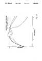
- FIG. 5shows graphically absorption vs. air gap thickness.
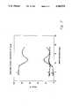
- FIG. 6shows absorption of entire structure vs. metal absorber thickness.
- FIG. 7shows measured optical properties of Si 3 N 4 .
- FIG. 1A cross section view of the two-level microbridge bolometer pixel 10 is shown in FIG. 1.
- the device 10has two levels, an elevated microbridge detector level 11 and a lower level 12.
- the lower levelhas a flat surfaced semiconductor substrate 13, such as a single crystal silicon substrate.
- the surface 14 of the substratehas fabricated thereon conventional components of an integrated circuit 15 such as diodes, bus lines, connections and contact pads (not specifically shown), the fabrication following conventional silicon IC technology.
- the ICis coated with a protective layer of silicon nitride 16.
- the elevated detector level 11includes a silicon nitride layer 20, a thin film resistive layer 21, preferably a vanadium or titanium oxide (such as V 2 O 3 , TiO x , VO x ), i.e. AB x a silicon nitride layer 22 over the layers 20 and 21 and an IR absorber coating 23 over the silicon nitride layer 22.
- the thin absorber coating(approximately 20A thick) may be of a nickel iron alloy, often called permalloy.
- Downwardly extending silicon nitride layers 20' and 22' deposited at the same time as layers 20 and 22 during the fabricationmake up the sloping supports 30 for the elevated detector level.
- the cavity or gap 26(approximately 1-2 microns high) between the two levels is ambient atmosphere.
- the cavity 26was originally filled with a previously deposited layer of easily dissolvable glass or other dissolvable material until the layers 20, 20', 22 and 22' were deposited.
- Some other easily dissolvable materialsare quartz, polyimide and resist.
- the glasswas dissolved out to provide the thermal isolation cavity or air gap (i.e., the air gap actually may be in operation, a vacuum gap).
- the horizontal dimension, as shown,is greatly foreshortened. That is, the height of FIG. 1 is exaggerated in the drawing compared to the length in order to show the details of the invention.
- FIG. 2is a top plan view of the elevated detector level 11. This drawing is made as though the overlying absorber coating 23 and the upper silicon nitride layer 22 are transparent so that the resistive thin film layer 21 can be shown.
- the material for the resistive layer 21is a vanadium oxide, preferably V 2 O 3 . Vanadium oxides have very strong changes in resistance with temperature allowing high sensitivity microbolometer operation. It also has a low reflectance to IR in the 8-14 micron range. In the preferred embodiment at this time the V 2 O 3 is operated in its semiconductor phase. Its deposition is preferably by the process of ion beam sputter which permits the deposition of very thin layers such as 50-75 mm.
- This materialwas thus selected for its low IR reflectance together with a relatively high temperature coefficient of resistance (TCR).
- TCRtemperature coefficient of resistance
- FIG. 2also shows nitride window cuts 35, 36 and 37 which are opened through the silicon nitride layers 20 and 22 to provide access to the phos-glass beneath for dissolving it from beneath the detector plane.
- the sloping supportsmay be of the necessary length is provide adequate support and thermal isolation for the upper level 11.
- each pixel assemblymay cover an area about 50 microns on a side, as an example.
- a sequence of fabrication steps for the upper levelis described. Following the deposition of the silicon nitride layer 16 in fabricating the lower level 12, a thin film layer 18 of reflective material, such as a metal film like Pt or Au, is deposited. The construction of the upper level can then commence.
- the detectors presently being describedare intended for use in the 8-14 micron IR wavelength.
- the reflective layer 18is on the lower plane 12.
- the vertical distance between reflective layer 18 and upper level 11is chosen so the reflected IR from layer 18 returned upwardly has interference properties such that significant absorption is achieved for a wide range of wavelengths (8-14 microns) and air gap spacing between the reflector and the detector structure.
- a layer of phos-glass or other easily soluble material in the range of about 1-2 microns thickis deposited and the slopes 30 and 30' are thoroughly rounded to eliminate slope coverage problems.
- the upper level silicon nitride base layer 20is then deposited, the resistive film 21 is deposited, connections down the slope to lower plane contact pads are made, and a silicon nitride passivation layer 22 covers the layers 21 and 20.
- a thin metal absorber coating 23(about 15-40A) is deposited on top of the upper level.
- the slots 35, 36 and 37, earlier mentionedare made and the phos-glass is dissolved from beneath the detector plane.
- Pt, Au or other reflecting thin film 18on the substrate before the stack is formed, it is possible to reflect transmitted radiation reaching the reflecting film back to the absorber coating.
- the optical properties of the total structureare achieved by careful selection of optical materials with the proper optical and electrical properties.
- the top filmmust reflect little radiation and generally transmit a significant percentage of the non-absorbed radiation through to the reflected light at a nodal position in the film determined by the air gap distance.
- An additional constraint on the absorbing filmis that to be compatible with the total structure, the absorbing material must be very thin (and hence have a low mass).
- the absorbing films in the present deviceconsist of ABx, SIN, and the thin absorbing metal described above.
- the ABx and SIN nitride thicknessesare chosen by electrical and physical requirements. Both have absorption levels ranging from 10-20% in the spectral region of interest (FIGS. 4 and 7). A combination of these materials produces an absorption of no more than about 30% in the 8-14 micron region. This absorption level is very close to ideal, however, for use with a Pt reflective layer and an air gap which intensifies the field in the absorbing film, it is possible to achieve absorptances in excess of 80% (FIG. 5) in this configuration.
- the use of a thin absorbing metal which in the standard design provides 50% absorption, hereis used to fine tune the absorption for maximum effect.
- FIG. 6shows the small absorption improvements that can be achieved by using this metal film.
- the low thermal mass structure 11is separated from the Pt/substrate layer by an air gap.
- the interference properties of this reflected radiationare such that significant absorption is achieved by a wide range of wavelengths and air gap spacing between the Pt reflector and the detector structure.
- gap thicknessThe effect of gap thickness on the absorptance vs. wavelength in the regions of interest are further displayed graphically in FIG. 5. It can be seen in the curve of 1.5 microns gap thickness that at 8 microns the absorptance of the structure is climbing rapidly towards 90% and more, and that it remains relatively high out to about 14 microns. The curve for a gap of 2 microns shows that at IR wavelengths of 14 microns the absorptance is better and well above 90%. In measuring the data for FIG. 5 the absorber film 23 was not included in the stack structure.
- FIG. 6there is shown graphically how the overall absorption of the film structure varies across the IR wavelength of 8-14 microns as the thickness of the metal absorber film is increased to 3 mm and to 5 mm.
- the Si 3 N 4 layer 22is 250 mm
- the resistive film 21is 75 nm
- the Si 3 N 4 film 20is 100 nm with an air gap of 1.5 microns and a reflective Pt layer 18 of 50 nm.
- This curve for 3 nmshows absorptance>90% between 8 and 14 microns.
- the measured optical properties of reflectance R, transmissivity T, and absorptance A of the silicon nitride layers 20 and 22 (800A thick)are shown in FIG. 7 with percent of signal shown on the ordinate axis and IR wavelength along the abscissa. It can be seen that the transmissivity at 8 microns (about 90) and at 14 microns (about 80) is quite high and that the reflectance R at both 8 and 14 microns is well under ten.
Landscapes
- Physics & Mathematics (AREA)
- General Physics & Mathematics (AREA)
- Spectroscopy & Molecular Physics (AREA)
- Photometry And Measurement Of Optical Pulse Characteristics (AREA)
Abstract
Description
The field of the invention is in a high sensitivity two-level microstructure infrared bolometer array which can produce absorptance levels of greater than 80% and also achieve high IR sensitivity over a wavelength range from 8-14 microns.
This invention is an improvement on co-pending application Ser. No. 887,495, filed Jul. 16, 1986, entitled "Thermal Sensor", and assigned to the same assignee as the present invention. The teachings of the co-pending application are incorporated herein by reference. In the co-pending application the invention is directed to a pixel size sensor of an array of sensors, for an infrared microbridge construction of high fill factor, made possible by placing the detector microbridge on a second plane above the silicon surface carrying the integrated components and bus lines. The improvement in the present invention is directed to a structure which increases the sensitivity.
FIGS. 1 and 2 are front and top views of a microstructure design according to the invention.
FIG. 3 is a graphical plot of overall absorptance vs. wavelength of the device over a selected wavelength including 8-14 microns.
FIG. 4 shows graphically the transmittance, absorption and reflectance of the resistive layer.
FIG. 5 shows graphically absorption vs. air gap thickness.
FIG. 6 shows absorption of entire structure vs. metal absorber thickness.
FIG. 7 shows measured optical properties of Si3 N4.
A cross section view of the two-levelmicrobridge bolometer pixel 10 is shown in FIG. 1. Thedevice 10 has two levels, an elevated microbridge detector level 11 and a lower level 12. The lower level has a flat surfacedsemiconductor substrate 13, such as a single crystal silicon substrate. Thesurface 14 of the substrate has fabricated thereon conventional components of an integratedcircuit 15 such as diodes, bus lines, connections and contact pads (not specifically shown), the fabrication following conventional silicon IC technology. The IC is coated with a protective layer ofsilicon nitride 16.
The elevated detector level 11 includes asilicon nitride layer 20, a thin filmresistive layer 21, preferably a vanadium or titanium oxide (such as V2 O3, TiOx, VOx), i.e. ABx asilicon nitride layer 22 over thelayers IR absorber coating 23 over thesilicon nitride layer 22. The thin absorber coating (approximately 20A thick) may be of a nickel iron alloy, often called permalloy. Downwardly extending silicon nitride layers 20' and 22' deposited at the same time aslayers cavity 26 was originally filled with a previously deposited layer of easily dissolvable glass or other dissolvable material until thelayers
FIG. 2 is a top plan view of the elevated detector level 11. This drawing is made as though theoverlying absorber coating 23 and the uppersilicon nitride layer 22 are transparent so that the resistivethin film layer 21 can be shown. In one preferred embodiment the material for theresistive layer 21 is a vanadium oxide, preferably V2 O3. Vanadium oxides have very strong changes in resistance with temperature allowing high sensitivity microbolometer operation. It also has a low reflectance to IR in the 8-14 micron range. In the preferred embodiment at this time the V2 O3 is operated in its semiconductor phase. Its deposition is preferably by the process of ion beam sputter which permits the deposition of very thin layers such as 50-75 mm. This material was thus selected for its low IR reflectance together with a relatively high temperature coefficient of resistance (TCR). The ends of the resistive paths 21a and 21b are continued down theslope area 30 embedded in 20' and 22' to make electrical contact withcontact pads
FIG. 2 also showsnitride window cuts silicon nitride layers
Although the description is basically in terms of individual detector pixels, the invention is directed for use to an x,y array assembly of adjoining pixels forming an imaging or mosaic detector array. Each pixel assembly may cover an area about 50 microns on a side, as an example.
Referring again to FIG. 1 a sequence of fabrication steps for the upper level is described. Following the deposition of thesilicon nitride layer 16 in fabricating the lower level 12, athin film layer 18 of reflective material, such as a metal film like Pt or Au, is deposited. The construction of the upper level can then commence. The detectors presently being described are intended for use in the 8-14 micron IR wavelength. Thereflective layer 18 is on the lower plane 12. The vertical distance betweenreflective layer 18 and upper level 11 is chosen so the reflected IR fromlayer 18 returned upwardly has interference properties such that significant absorption is achieved for a wide range of wavelengths (8-14 microns) and air gap spacing between the reflector and the detector structure.
A layer of phos-glass or other easily soluble material in the range of about 1-2 microns thick is deposited and theslopes 30 and 30' are thoroughly rounded to eliminate slope coverage problems. The upper level siliconnitride base layer 20 is then deposited, theresistive film 21 is deposited, connections down the slope to lower plane contact pads are made, and a siliconnitride passivation layer 22 covers thelayers slots thin film 18 on the substrate before the stack is formed, it is possible to reflect transmitted radiation reaching the reflecting film back to the absorber coating.
The optical properties of the total structure are achieved by careful selection of optical materials with the proper optical and electrical properties. The top film must reflect little radiation and generally transmit a significant percentage of the non-absorbed radiation through to the reflected light at a nodal position in the film determined by the air gap distance. An additional constraint on the absorbing film is that to be compatible with the total structure, the absorbing material must be very thin (and hence have a low mass).
To optimize the absorption in the structure, the thickness of all the absorbing layers and the air gap distance must be controlled. The absorbing films in the present device consist of ABx, SIN, and the thin absorbing metal described above. In practice, the ABx and SIN nitride thicknesses are chosen by electrical and physical requirements. Both have absorption levels ranging from 10-20% in the spectral region of interest (FIGS. 4 and 7). A combination of these materials produces an absorption of no more than about 30% in the 8-14 micron region. This absorption level is very close to ideal, however, for use with a Pt reflective layer and an air gap which intensifies the field in the absorbing film, it is possible to achieve absorptances in excess of 80% (FIG. 5) in this configuration. The use of a thin absorbing metal which in the standard design provides 50% absorption, here is used to fine tune the absorption for maximum effect. FIG. 6 shows the small absorption improvements that can be achieved by using this metal film.
In this two-level structure, the low thermal mass structure 11 is separated from the Pt/substrate layer by an air gap. The interference properties of this reflected radiation are such that significant absorption is achieved by a wide range of wavelengths and air gap spacing between the Pt reflector and the detector structure.
For this optical interference to occur in the detector, it is necessary to avoid other films in the detector structure which reflect IR. The use of ABx which has both a high TCR and a low IR reflectance (FIG. 4) ideally meets these requirements. Thus the merging of this absorption phenomenon into a detector structure which has a detector material processing both a high TCR and low reflectance permits this interference effect to occur.
There is a substantial degree of variability of detector absorptance with air gap in the structure. Referring to the table below which shows wavelength in nanometers in the left column vs. air gap in microns across the top it can be seen that with an air gap of only 0.5 micron the detector absorptance varies widely with wavelength and it is not very high. With air gaps of 1-2 microns and especially at 1.5 microns the absorptance is relatively high across the desired wavelength spread.
TABLE 1 ______________________________________ DETECTOR ABSORPTANCE Air Gap (microns) ______________________________________ Wavelength(NM) .5 .75 1.0 1.5 2.0 8000 .89 .91 .9 .84 .76 9000 .84 .88 .89 .86 .81 10000 .76 .82 .84 .84 .82 11000 .69 .77 .8 .82 .82 12000 .66 .74 .79 .83 .84 13000 .64 .78 .85 .93 .94 14000 .56 .72 .83 .95 .98 15000 .47 .64 .77 .92 .99 ______________________________________
The effect of gap thickness on the absorptance vs. wavelength in the regions of interest are further displayed graphically in FIG. 5. It can be seen in the curve of 1.5 microns gap thickness that at 8 microns the absorptance of the structure is climbing rapidly towards 90% and more, and that it remains relatively high out to about 14 microns. The curve for a gap of 2 microns shows that at IR wavelengths of 14 microns the absorptance is better and well above 90%. In measuring the data for FIG. 5 theabsorber film 23 was not included in the stack structure.
Referring now to FIG. 6 there is shown graphically how the overall absorption of the film structure varies across the IR wavelength of 8-14 microns as the thickness of the metal absorber film is increased to 3 mm and to 5 mm. In this film stack design the Si3 N4 layer 22 is 250 mm, theresistive film 21 is 75 nm and the Si3 N4 film 20 is 100 nm with an air gap of 1.5 microns and areflective Pt layer 18 of 50 nm. This curve for 3 nm shows absorptance>90% between 8 and 14 microns.
The measured optical properties of reflectance R, transmissivity T, and absorptance A of the silicon nitride layers 20 and 22 (800A thick) are shown in FIG. 7 with percent of signal shown on the ordinate axis and IR wavelength along the abscissa. It can be seen that the transmissivity at 8 microns (about 90) and at 14 microns (about 80) is quite high and that the reflectance R at both 8 and 14 microns is well under ten.
Claims (12)
1. A two-level microbridge infrared bolometer structure comprising:
a bolometer structure on a semiconductor substrate, said structure having a lower section on the surface of the substrate and a microbridge upper detector plane structure spaced from and immediately above the lower section;
an infrared-reflective thin film metal coating on the surface of said lower section;
said upper microbridge detector plane structure comprising a planar sandwich structure including a supporting dielectric thin film layer, and a thin film temperature responsive resistive element having first and second terminals;
downwardly extending dielectric leg portion means which are a downwardly extending continuation of said upper structure dielectric supporting said upper microbridge detector plane structure above said lower section so that a thermal isolation gap exists between said upper and lower sections; and,
electrically conductive paths included in said downwardly extending leg portion means connecting said first and second terminals to said lower section.
2. The microbridge structure according to claim 1 wherein said reflective thin film metal coating is selected from the group consisting of Au, Pt, and Al.
3. The microbridge structure according to claim 1 wherein said dielectric is of silicon nitride.
4. The microbridge structure according to claim 1 wherein said thin film resistive element is selected from the group consisting of vanadium oxide and titanium oxide.
5. The microbridge structure according to claim 1 wherein said thin film resistive element is V2 O3.
6. The microbridge structure according to claim 1 wherein said gap between said lower section and said upper detector structure is in the range of about 1-2 microns.
7. The microbridge structure according to claim 2 wherein the coating is about 50 nm in thickness.
8. The microbridge structure according to claim 1 and further comprising, in said planar sandwich structure, a second dielectric thin film layer and a thin film absorber layer.
9. The microbridge structure according to claim 3 wherein the first dielectric layer in on the order of 100 nm in thickness and the second dielectric layer is on the order of 250 nm in thickness.
10. The microbridge structure according to claim 4 wherein the resistive element film is on the order of 50-75 nm in thickness.
11. The microbridge structure according to claim 8 wherein the absorber layer is on the order of 30 nm in thickness.
12. A two-level microbridge infrared bolometer structure comprising:
a bolometer microstructure on a semiconductor substrate, said structure having a lower section on the surface of the substrate and a microbridge upper detector plane structure spaced from and immediately above the lower section;
an infrared reflective thin film metal coating on the surface of said lower section, said metal being selected from the group consisting of Au, Pt, and Al;
said upper microbridge detector plane structure comprising a planar sandwich structure including a first bridging dielectric thin film layer, a thin film temperature responsive resistive element selected from the group consisting of vanadium oxide
and titanium oxide, said resistive element having first and second terminals, a second dielectric thin film layer over said first dielectric layer and resistive layer, and a thin film absorber layer;
downwardly extending dielectric leg portion means which are a downwardly extending continuation of said upper structure dielectric supporting said upper microbridge detector plane structure above said lower section so that an air gap on the order of 1-2 microns exists between said upper and lower sections; and,
electrically conductive paths included in said downwardly extending leg portion means connecting said first and second terminals to said lower section.
Priority Applications (2)
| Application Number | Priority Date | Filing Date | Title |
|---|---|---|---|
| US07/288,701US5286976A (en) | 1988-11-07 | 1988-11-07 | Microstructure design for high IR sensitivity |
| US08/601,411USRE36706E (en) | 1988-11-07 | 1996-02-14 | Microstructure design for high IR sensitivity |
Applications Claiming Priority (1)
| Application Number | Priority Date | Filing Date | Title |
|---|---|---|---|
| US07/288,701US5286976A (en) | 1988-11-07 | 1988-11-07 | Microstructure design for high IR sensitivity |
Related Child Applications (1)
| Application Number | Title | Priority Date | Filing Date |
|---|---|---|---|
| US08/601,411ReissueUSRE36706E (en) | 1988-11-07 | 1996-02-14 | Microstructure design for high IR sensitivity |
Publications (1)
| Publication Number | Publication Date |
|---|---|
| US5286976Atrue US5286976A (en) | 1994-02-15 |
Family
ID=23108254
Family Applications (2)
| Application Number | Title | Priority Date | Filing Date |
|---|---|---|---|
| US07/288,701CeasedUS5286976A (en) | 1988-11-07 | 1988-11-07 | Microstructure design for high IR sensitivity |
| US08/601,411Expired - LifetimeUSRE36706E (en) | 1988-11-07 | 1996-02-14 | Microstructure design for high IR sensitivity |
Family Applications After (1)
| Application Number | Title | Priority Date | Filing Date |
|---|---|---|---|
| US08/601,411Expired - LifetimeUSRE36706E (en) | 1988-11-07 | 1996-02-14 | Microstructure design for high IR sensitivity |
Country Status (1)
| Country | Link |
|---|---|
| US (2) | US5286976A (en) |
Cited By (118)
| Publication number | Priority date | Publication date | Assignee | Title |
|---|---|---|---|---|
| US5446284A (en)* | 1994-01-25 | 1995-08-29 | Loral Infrared & Imaging Systems, Inc. | Monolithic detector array apparatus |
| US5489776A (en)* | 1994-08-30 | 1996-02-06 | Hughes Aircraft Company | Microbolometer unit cell signal processing circuit |
| WO1996021140A1 (en)* | 1994-12-30 | 1996-07-11 | Honeywell Inc. | Fabry-perot micro filter-detector |
| US5541412A (en)* | 1993-11-24 | 1996-07-30 | Nec Corporation | Two dimensional array infrared ray image pickup device |
| US5554849A (en)* | 1995-01-17 | 1996-09-10 | Flir Systems, Inc. | Micro-bolometric infrared staring array |
| US5561295A (en)* | 1994-07-29 | 1996-10-01 | Litton Systems, Inc. | Infrared-responsive photoconductive array and method of making |
| US5572060A (en)* | 1995-02-01 | 1996-11-05 | Southern Methodist University | Uncooled YBaCuO thin film infrared detector |
| US5584117A (en)* | 1995-12-11 | 1996-12-17 | Industrial Technology Research Institute | Method of making an interferometer-based bolometer |
| US5602393A (en)* | 1995-06-07 | 1997-02-11 | Hughes Aircraft Company | Microbolometer detector element with enhanced sensitivity |
| US5608568A (en)* | 1994-04-11 | 1997-03-04 | The Johns Hopkins University | Thin film vanadium oxide spatial light modulators and methods |
| WO1997018589A1 (en)* | 1995-11-15 | 1997-05-22 | Lockheed-Martin Ir Imaging Systems, Inc. | A dual-band multi-level microbridge detector |
| WO1997021250A1 (en)* | 1995-12-04 | 1997-06-12 | Lockheed-Martin Ir Imaging Systems, Inc. | Infrared radiation detector having a reduced active area |
| US5640013A (en)* | 1995-04-07 | 1997-06-17 | Mitsubishi Denki Kabushiki Kaisha | Infrared sensor having a heat sensitive semiconductor portion that detects and absorbs infrared rays |
| EP0784205A1 (en)* | 1996-01-05 | 1997-07-16 | Xerox Corporation | Thermal sensor arrays useful for motion tracking by thermal gradient detection |
| US5693942A (en)* | 1995-04-07 | 1997-12-02 | Ishizuka Electronics Corporation | Infrared detector |
| US5698852A (en)* | 1994-08-11 | 1997-12-16 | Nec Corporation | Titanium bolometer-type infrared detecting apparatus |
| WO1998011611A1 (en)* | 1996-09-12 | 1998-03-19 | Institut National D'optique | Microbridge structure, and method for forming a microbridge suspended by a micro support |
| US5756999A (en)* | 1997-02-11 | 1998-05-26 | Indigo Systems Corporation | Methods and circuitry for correcting temperature-induced errors in microbolometer focal plane array |
| WO1998035212A1 (en)* | 1997-02-11 | 1998-08-13 | Indigo Systems Corporation | Methods and circuitry for correcting temperature-induced errors in microbolometer focal plane array |
| US5811808A (en)* | 1996-09-12 | 1998-09-22 | Amber Engineering, Inc. | Infrared imaging system employing on-focal plane nonuniformity correction |
| EP0869341A1 (en)* | 1997-03-31 | 1998-10-07 | Nec Corporation | Thermal infrared detecting device |
| US5831266A (en)* | 1996-09-12 | 1998-11-03 | Institut National D'optique | Microbridge structure for emitting or detecting radiations and method for forming such microbridge structure |
| US5850098A (en)* | 1995-02-01 | 1998-12-15 | Research Corporation Technologies, Inc. | Uncooled amorphous YBaCuO thin film infrared detector |
| WO1999005723A1 (en)* | 1997-07-25 | 1999-02-04 | Honeywell Inc. | A dual bandwidth bolometer |
| US5900799A (en)* | 1997-10-03 | 1999-05-04 | Mcdonnell Douglas Corporation | High responsivity thermochromic infrared detector |
| US5973383A (en)* | 1998-04-09 | 1999-10-26 | Honeywell Inc. | High temperature ZrN and HfN IR scene projector pixels |
| EP0977275A1 (en)* | 1998-07-28 | 2000-02-02 | Commissariat A L'energie Atomique | Infrared/visible multispectral radiation detector |
| US6034369A (en)* | 1996-11-27 | 2000-03-07 | Nec Corporation | Thermal infrared detecting device capable of detecting infrared rays without influence of operating temperature |
| US6046485A (en)* | 1999-04-01 | 2000-04-04 | Honeywell International Inc. | Large area low mass IR pixel having tailored cross section |
| WO2000033041A1 (en)* | 1998-11-30 | 2000-06-08 | Daewoo Electronics Co., Ltd. | Infrared bolometer |
| US6144285A (en)* | 1999-09-13 | 2000-11-07 | Honeywell International Inc. | Thermal sensor and method of making same |
| US6144030A (en)* | 1997-10-28 | 2000-11-07 | Raytheon Company | Advanced small pixel high fill factor uncooled focal plane array |
| US6165587A (en)* | 1997-09-09 | 2000-12-26 | Honda Giken Kogyo Kabushiki Kaisha | Microbridge structure with reinforcement section |
| US6194722B1 (en) | 1997-03-28 | 2001-02-27 | Interuniversitair Micro-Elektronica Centrum, Imec, Vzw | Method of fabrication of an infrared radiation detector and infrared detector device |
| US6198099B1 (en)* | 1998-08-31 | 2001-03-06 | Daewoo Electronics Co., Ltd. | Bolometer including a reflective layer |
| US6201244B1 (en)* | 1998-08-31 | 2001-03-13 | Daewoo Electronics Co., Ltd. | Bolometer including an absorber made of a material having a low deposition-temperature and a low heat-conductivity |
| US6201243B1 (en) | 1998-07-20 | 2001-03-13 | Institut National D'optique | Microbridge structure and method for forming the microbridge structure |
| US6211520B1 (en) | 1998-10-19 | 2001-04-03 | Mitsubishi Denki Kabushiki Kaisha | Infrared sensor and infrared sensor array using the same |
| US6218667B1 (en) | 1997-09-09 | 2001-04-17 | Honda Giken Kogyo Kabushiki Kaisha | Sensor element with small area light detecting section of bridge structure |
| US6225629B1 (en)* | 1998-08-31 | 2001-05-01 | Daewoo Electronics Co., Ltd. | Bolometer with a serpentine stress balancing member |
| US6307194B1 (en) | 1999-06-07 | 2001-10-23 | The Boeing Company | Pixel structure having a bolometer with spaced apart absorber and transducer layers and an associated fabrication method |
| US6329696B1 (en) | 1997-06-11 | 2001-12-11 | Nec Corporation | Semiconductor device with electric converter element |
| FR2811139A1 (en)* | 2000-06-29 | 2002-01-04 | Centre Nat Rech Scient | OPTOELECTRONIC DEVICE WITH INTEGRATED WAVELENGTH FILTERING |
| US6353223B1 (en) | 1998-09-10 | 2002-03-05 | Mitsubishi Denki Kabushiki Kaisha | Infrared camera |
| WO2002040954A1 (en)* | 2000-11-15 | 2002-05-23 | The Boeing Company | Reference bolometer and associated fabrication methods |
| WO2002043154A1 (en)* | 2000-11-27 | 2002-05-30 | Siemens Aktiengesellschaft | Pyroelectric image sensor and method for producing the same |
| US6444983B1 (en) | 1999-10-07 | 2002-09-03 | Infrared Solutions, Inc. | Microbolometer focal plane array with controlled bias |
| US6459084B1 (en) | 1997-05-30 | 2002-10-01 | University Of Central Florida | Area receiver with antenna-coupled infrared sensors |
| US6465785B1 (en) | 2000-05-05 | 2002-10-15 | Infrared Solutions, Inc. | Apparatus and method for compensating for pixel non-uniformity in a bolometer |
| US6465784B1 (en) | 1997-12-18 | 2002-10-15 | Mitsubishi Denki Kabushiki Kaisha | Infrared solid-state imaging sensing device |
| US6479320B1 (en) | 2000-02-02 | 2002-11-12 | Raytheon Company | Vacuum package fabrication of microelectromechanical system devices with integrated circuit components |
| US6489616B2 (en) | 2001-03-19 | 2002-12-03 | The Board Of Governors Of Southwest Missouri State University | Doped, organic carbon-containing sensor for infrared detection and a process for the preparation thereof |
| US6489613B1 (en) | 1998-09-01 | 2002-12-03 | Nec Corporation | Oxide thin film for bolometer and infrared detector using the oxide thin film |
| WO2002099155A1 (en)* | 2001-06-01 | 2002-12-12 | Honeywell International Inc. | Ion beam sputter deposition process |
| US6495070B1 (en) | 1996-12-31 | 2002-12-17 | Honeywell International Inc. | Flexible high performance microbolometer detector material fabricated via controlled ion beam sputter deposition process |
| US6521477B1 (en) | 2000-02-02 | 2003-02-18 | Raytheon Company | Vacuum package fabrication of integrated circuit components |
| US6531699B1 (en)* | 1999-06-04 | 2003-03-11 | Thomson-Csf | Heat detector with a limited angle of vision |
| US6541772B2 (en) | 2000-12-26 | 2003-04-01 | Honeywell International Inc. | Microbolometer operating system |
| US6552344B1 (en) | 1999-11-30 | 2003-04-22 | Mitsubishi Denki Kabushiki Kaisha | Infrared detector and method of making the infrared detector |
| US6559447B2 (en) | 2000-12-26 | 2003-05-06 | Honeywell International Inc. | Lightweight infrared camera |
| US20030124761A1 (en)* | 1997-03-28 | 2003-07-03 | Kris Baert | Method for depositing polycrystalline sige suitable for micromachining and devices obtained thereof |
| US20030197124A1 (en)* | 2000-12-26 | 2003-10-23 | Honeywell International Inc. | Camera having distortion correction |
| US6690012B1 (en) | 2000-10-13 | 2004-02-10 | Litton Systems, Inc. | Hybridized lead-salt infrared radiation detectors and methods of formation |
| US6690014B1 (en) | 2000-04-25 | 2004-02-10 | Raytheon Company | Microbolometer and method for forming |
| US20040027938A1 (en)* | 2002-07-25 | 2004-02-12 | Pioneer Corporation | Spherical aberration correcting method and apparatus |
| US6770882B2 (en)* | 2002-01-14 | 2004-08-03 | Multispectral Imaging, Inc. | Micromachined pyro-optical structure |
| US6777681B1 (en) | 2001-04-25 | 2004-08-17 | Raytheon Company | Infrared detector with amorphous silicon detector elements, and a method of making it |
| US20040218187A1 (en)* | 2002-03-18 | 2004-11-04 | Cole Barrett E. | Multiple wavelength spectrometer |
| EP0903566B1 (en)* | 1997-09-16 | 2004-12-01 | Metorex International OY | Imaging system functioning on submillimeter waves |
| US20040240012A1 (en)* | 2003-05-26 | 2004-12-02 | Fuji Xerox Co., Ltd. | Hologram recording method and hologram recording apparatus |
| US20050017177A1 (en)* | 2003-04-11 | 2005-01-27 | California Institute Of Technology | Apparatus and method for sensing electromagnetic radiation using a tunable device |
| US20050072924A1 (en)* | 2003-10-03 | 2005-04-07 | Honeywell International Inc. | Planar thermal array |
| US20050147533A1 (en)* | 2003-12-30 | 2005-07-07 | Cole Barrett E. | Particle detector using fluorescents |
| US6958478B2 (en) | 2003-05-19 | 2005-10-25 | Indigo Systems Corporation | Microbolometer detector with high fill factor and transducers having enhanced thermal isolation |
| US20050238080A1 (en)* | 2002-04-01 | 2005-10-27 | Palo Alto Research Center Incorporated | Resistive thermal sensing |
| WO2005094460A3 (en)* | 2004-03-23 | 2005-12-29 | Bae Systems Information | Multi-spectral uncooled microbolometer detectors |
| US7002153B1 (en) | 1999-08-24 | 2006-02-21 | Qinetiq Limited | Micro-bridge structure |
| US7005644B2 (en) | 2003-04-11 | 2006-02-28 | Mitsubishi Denki Kabushiki Kaisha | Thermal infrared detector and infrared focal plane array |
| US7030453B1 (en)* | 1998-12-30 | 2006-04-18 | Commissariat A L'energie Atomique | Bolometric detector with an antenna |
| US20060232674A1 (en)* | 2001-05-21 | 2006-10-19 | Cochran Don W | Apparatus and method for providing snapshot action thermal infrared imaging within automated process control article inspection applications |
| EP1727359A2 (en) | 2005-05-26 | 2006-11-29 | Infrared Solutions, Inc. | Method for fixed pattern noise reduction in infrared imaging cameras |
| AU2004203904B2 (en)* | 1999-09-13 | 2007-02-01 | Honeywell Inc. | Thermal sensor and method of making same |
| US20070120058A1 (en)* | 1995-10-24 | 2007-05-31 | Bae, Inc. | Uncooled infrared sensor |
| US20070170363A1 (en)* | 2006-01-26 | 2007-07-26 | Schimert Thomas R | Infrared detector elements and methods of forming same |
| US20070170359A1 (en)* | 2006-01-26 | 2007-07-26 | Syllaios Athanasios J | Systems and methods for integrating focal plane arrays |
| US20070170360A1 (en)* | 2006-01-26 | 2007-07-26 | Gooch Roland W | Systems and methods for bonding |
| US20080035846A1 (en)* | 2006-05-23 | 2008-02-14 | Joseph Talghader | Tunable finesse infrared cavity thermal detectors |
| US20080185522A1 (en)* | 2007-02-06 | 2008-08-07 | Shih-Chia Chang | Infrared sensors and methods for manufacturing the infrared sensors |
| US20080217539A1 (en)* | 2006-12-08 | 2008-09-11 | Talghader Joseph J | Detection beyond the standard radiation noise limit using reduced emissivity and optical cavity coupling |
| EP2037243A2 (en) | 2007-09-13 | 2009-03-18 | Honeywell International Inc. | Nanowire multispectral imaging array |
| US7527999B2 (en) | 2005-12-06 | 2009-05-05 | Technion Research & Development Foundation Ltd. | Cd1−xZnxS high performance TCR material for uncooled microbolometers used in infrared sensors and method of making same |
| US20090140147A1 (en)* | 2007-08-22 | 2009-06-04 | Skidmore George D | Pixel structure having an umbrella type absorber with one or more recesses or channels sized to increase radiation absorption |
| US7718965B1 (en) | 2006-08-03 | 2010-05-18 | L-3 Communications Corporation | Microbolometer infrared detector elements and methods for forming same |
| EP1482289B1 (en)* | 2003-05-26 | 2010-06-02 | Commissariat à l'énergie atomique et aux énergies alternatives | Bolometric detection method of (sub-)millimeter waves using an antenna coupled bolometer having a cavity |
| US7750301B1 (en) | 2007-10-02 | 2010-07-06 | Flir Systems, Inc. | Microbolometer optical cavity tuning and calibration systems and methods |
| US20110050642A1 (en)* | 2009-08-26 | 2011-03-03 | Lee Sang-Myoung | Touch sensing electrophoretic display device |
| US20110049366A1 (en)* | 2009-09-02 | 2011-03-03 | Electronics And Telecommunications Research Institute | Resistive material for bolometer, bolometer for infrared detector using the material, and method of manufacturing the bolometer |
| US20110108729A1 (en)* | 2009-11-12 | 2011-05-12 | Naoki Oda | THz WAVE DETECTOR |
| US20110266445A1 (en)* | 2010-04-28 | 2011-11-03 | Howard Beratan | Optically transitioning thermal detector structures |
| US8153980B1 (en) | 2006-11-30 | 2012-04-10 | L-3 Communications Corp. | Color correction for radiation detectors |
| CN102610619A (en)* | 2012-03-29 | 2012-07-25 | 江苏物联网研究发展中心 | Wafer-level vacuum encapsulated infrared focal plane array (IRFPA) device and method for producing same |
| US8610070B2 (en) | 2010-04-28 | 2013-12-17 | L-3 Communications Corporation | Pixel-level optical elements for uncooled infrared detector devices |
| US8629398B2 (en) | 2008-05-30 | 2014-01-14 | The Regents Of The University Of Minnesota | Detection beyond the standard radiation noise limit using spectrally selective absorption |
| US8729474B1 (en) | 2009-10-09 | 2014-05-20 | Flir Systems, Inc. | Microbolometer contact systems and methods |
| US8743596B2 (en) | 2012-11-05 | 2014-06-03 | International Business Machines Corporation | Magnetoresistive random access memory |
| US8765514B1 (en) | 2010-11-12 | 2014-07-01 | L-3 Communications Corp. | Transitioned film growth for conductive semiconductor materials |
| US20150034825A1 (en)* | 2012-03-08 | 2015-02-05 | Canon Kabushiki Kaisha | Device for radiating or receiving electromagnetic waves |
| US9167179B2 (en) | 2011-02-21 | 2015-10-20 | Vectronix, Inc. | On-board non-uniformity correction calibration methods for microbolometer focal plane arrays |
| EA022126B1 (en)* | 2013-02-18 | 2015-11-30 | Государственное Научное Учреждение "Институт Тепло- И Массообмена Имени А.В. Лыкова Национальной Академии Наук Беларуси" | Method of measuring radiant heat flux in vacuum |
| US9250135B2 (en) | 2011-03-16 | 2016-02-02 | Honeywell International Inc. | MWIR sensor for flame detection |
| US9324937B1 (en) | 2015-03-24 | 2016-04-26 | International Business Machines Corporation | Thermally assisted MRAM including magnetic tunnel junction and vacuum cavity |
| US9658111B2 (en) | 2009-10-09 | 2017-05-23 | Flir Systems, Inc. | Microbolometer contact systems and methods |
| DE102017222480A1 (en) | 2017-05-24 | 2018-11-29 | Mitsubishi Electric Corporation | INFRARED SENSOR AND INFRARED SEMICONDUCTOR IMAGE RECORDING DEVICE |
| US20190145830A1 (en)* | 2016-07-18 | 2019-05-16 | Shanghai Ic R&D Center Co., Ltd. | Infrared detector pixel structure and manufactureing method thereof |
| US10359316B1 (en)* | 2016-06-08 | 2019-07-23 | Nutech Ventures, Inc. | Fiber optic bolometer |
| CN110118605A (en)* | 2019-05-30 | 2019-08-13 | 中国科学院长春光学精密机械与物理研究所 | A kind of mode of resonance wide spectrum non-refrigerated infrared detector and preparation method thereof |
| CN110332998A (en)* | 2019-06-17 | 2019-10-15 | 华中科技大学 | Metamaterial uncooled infrared focal plane polychromatic polarization detector and its preparation method |
| US10852193B2 (en) | 2017-11-16 | 2020-12-01 | Mitsubishi Electric Corporation | Thermal infrared detector and manufacturing method thereof |
Families Citing this family (12)
| Publication number | Priority date | Publication date | Assignee | Title |
|---|---|---|---|---|
| JP3460810B2 (en)* | 1999-07-26 | 2003-10-27 | 日本電気株式会社 | Thermal infrared detector with thermal separation structure |
| US6621083B2 (en)* | 2000-12-29 | 2003-09-16 | Honeywell International Inc. | High-absorption wide-band pixel for bolometer arrays |
| US6667479B2 (en) | 2001-06-01 | 2003-12-23 | Raytheon Company | Advanced high speed, multi-level uncooled bolometer and method for fabricating same |
| JP2003106895A (en)* | 2001-10-01 | 2003-04-09 | Nec Corp | Thermal infrared detecting element and method of manufacturing the same |
| US7145143B2 (en)* | 2002-03-18 | 2006-12-05 | Honeywell International Inc. | Tunable sensor |
| US20040084308A1 (en)* | 2002-11-01 | 2004-05-06 | Cole Barrett E. | Gas sensor |
| US7442933B2 (en) | 2005-02-03 | 2008-10-28 | Lin Alice L | Bolometer having an amorphous titanium oxide layer with high resistance stability |
| US7746236B2 (en)* | 2007-05-01 | 2010-06-29 | Honeywell International Inc. | Fire detection system and method |
| US20090014657A1 (en)* | 2007-05-01 | 2009-01-15 | Honeywell International Inc. | Infrared fire detection system |
| US7842533B2 (en)* | 2009-01-07 | 2010-11-30 | Robert Bosch Gmbh | Electromagnetic radiation sensor and method of manufacture |
| US8314769B2 (en) | 2010-04-28 | 2012-11-20 | Honeywell International Inc. | High performance detection pixel |
| US8502147B2 (en) | 2011-10-04 | 2013-08-06 | Flir Systems, Inc. | Microbolometer detector layer |
Citations (1)
| Publication number | Priority date | Publication date | Assignee | Title |
|---|---|---|---|---|
| US5021663A (en)* | 1988-08-12 | 1991-06-04 | Texas Instruments Incorporated | Infrared detector |
Family Cites Families (32)
| Publication number | Priority date | Publication date | Assignee | Title |
|---|---|---|---|---|
| US3484611A (en)* | 1967-05-16 | 1969-12-16 | Hitachi Ltd | Infrared detector composed of a sintered body of vanadium pentoxide and vanadium oxide |
| JPS4821363B1 (en)* | 1967-12-31 | 1973-06-28 | ||
| FR1600335A (en)* | 1968-12-31 | 1970-07-20 | ||
| US3693011A (en)* | 1971-02-02 | 1972-09-19 | Hughes Aircraft Co | Ion implanted bolometer |
| US3851174A (en)* | 1973-05-04 | 1974-11-26 | Ibm | Light detector for the nanosecond-dc pulse width range |
| US3896309A (en)* | 1973-05-21 | 1975-07-22 | Westinghouse Electric Corp | Radiation detecting device |
| US4029962A (en)* | 1975-06-23 | 1977-06-14 | Texas Instruments Incorporated | Arrays for infrared image detection |
| US4009516A (en)* | 1976-03-29 | 1977-03-01 | Honeywell Inc. | Pyroelectric detector fabrication |
| US4067104A (en)* | 1977-02-24 | 1978-01-10 | Rockwell International Corporation | Method of fabricating an array of flexible metallic interconnects for coupling microelectronics components |
| US4115692A (en)* | 1977-05-04 | 1978-09-19 | The United States Of America As Represented By The Secretary Of The Army | Solid state readout device for a two dimensional pyroelectric detector array |
| US4286278A (en)* | 1977-09-01 | 1981-08-25 | Honeywell Inc. | Hybrid mosaic IR/CCD focal plane |
| US4169273A (en)* | 1978-06-26 | 1979-09-25 | Honeywell Inc. | Photodetector signal processing |
| US4239312A (en)* | 1978-11-29 | 1980-12-16 | Hughes Aircraft Company | Parallel interconnect for planar arrays |
| US4365106A (en)* | 1979-08-24 | 1982-12-21 | Pulvari Charles F | Efficient method and apparatus for converting solar energy to electrical energy |
| US4354109A (en)* | 1979-12-31 | 1982-10-12 | Honeywell Inc. | Mounting for pyroelectric detecctor arrays |
| US4317126A (en)* | 1980-04-14 | 1982-02-23 | Motorola, Inc. | Silicon pressure sensor |
| US4378489A (en)* | 1981-05-18 | 1983-03-29 | Honeywell Inc. | Miniature thin film infrared calibration source |
| US4472239A (en)* | 1981-10-09 | 1984-09-18 | Honeywell, Inc. | Method of making semiconductor device |
| JPS5864044A (en)* | 1981-10-14 | 1983-04-16 | Toshiba Corp | Manufacturing method of semiconductor device |
| JPS58131525A (en)* | 1982-01-31 | 1983-08-05 | Matsushita Electric Works Ltd | infrared detection device |
| JPS60119426A (en)* | 1983-12-01 | 1985-06-26 | Murata Mfg Co Ltd | Thin film type pyroelectric sensor array |
| JPH073362B2 (en)* | 1984-06-14 | 1995-01-18 | 株式会社村田製作所 | One-dimensional pyroelectric sensor array |
| GB2164789B (en)* | 1984-09-19 | 1987-11-11 | Philips Electronic Associated | Pyroelectric infra-red detector |
| JPS61170626A (en)* | 1985-01-24 | 1986-08-01 | Matsushita Electric Ind Co Ltd | Infrared linear array element |
| JPS61195318A (en)* | 1985-02-26 | 1986-08-29 | Matsushita Electric Ind Co Ltd | Pyroelectric type infrared detector |
| US5017784A (en)* | 1985-03-11 | 1991-05-21 | Savin Corporation | Thermal detector |
| US5455421A (en)* | 1985-08-13 | 1995-10-03 | Massachusetts Institute Of Technology | Infrared detector using a resonant optical cavity for enhanced absorption |
| US4750834A (en)* | 1986-01-07 | 1988-06-14 | D.O.M. Associates, Inc. | Interferometer including stationary, electrically alterable optical masking device |
| JPH01136035A (en)* | 1987-11-24 | 1989-05-29 | Hamamatsu Photonics Kk | Manufacturing method of pyroelectric detection element |
| US5010251A (en)* | 1988-08-04 | 1991-04-23 | Hughes Aircraft Company | Radiation detector array using radiation sensitive bridges |
| JPH0341305A (en)* | 1989-07-07 | 1991-02-21 | Matsushita Electric Ind Co Ltd | Pyroelectric device for detecting infrared ray |
| DE69123575T2 (en)* | 1990-04-26 | 1999-09-02 | The Commonwealth Of Australia | BOLOMETER TYPE THERMAL INFRARED DETECTOR WITH SEMICONDUCTOR FILM |
- 1988
- 1988-11-07USUS07/288,701patent/US5286976A/ennot_activeCeased
- 1996
- 1996-02-14USUS08/601,411patent/USRE36706E/ennot_activeExpired - Lifetime
Patent Citations (2)
| Publication number | Priority date | Publication date | Assignee | Title |
|---|---|---|---|---|
| US5021663A (en)* | 1988-08-12 | 1991-06-04 | Texas Instruments Incorporated | Infrared detector |
| US5021663B1 (en)* | 1988-08-12 | 1997-07-01 | Texas Instruments Inc | Infrared detector |
Cited By (183)
| Publication number | Priority date | Publication date | Assignee | Title |
|---|---|---|---|---|
| US5541412A (en)* | 1993-11-24 | 1996-07-30 | Nec Corporation | Two dimensional array infrared ray image pickup device |
| US5446284A (en)* | 1994-01-25 | 1995-08-29 | Loral Infrared & Imaging Systems, Inc. | Monolithic detector array apparatus |
| US5608568A (en)* | 1994-04-11 | 1997-03-04 | The Johns Hopkins University | Thin film vanadium oxide spatial light modulators and methods |
| US5561295A (en)* | 1994-07-29 | 1996-10-01 | Litton Systems, Inc. | Infrared-responsive photoconductive array and method of making |
| US5698852A (en)* | 1994-08-11 | 1997-12-16 | Nec Corporation | Titanium bolometer-type infrared detecting apparatus |
| US5489776A (en)* | 1994-08-30 | 1996-02-06 | Hughes Aircraft Company | Microbolometer unit cell signal processing circuit |
| WO1996021140A1 (en)* | 1994-12-30 | 1996-07-11 | Honeywell Inc. | Fabry-perot micro filter-detector |
| US5554849A (en)* | 1995-01-17 | 1996-09-10 | Flir Systems, Inc. | Micro-bolometric infrared staring array |
| US5572060A (en)* | 1995-02-01 | 1996-11-05 | Southern Methodist University | Uncooled YBaCuO thin film infrared detector |
| US5672903A (en)* | 1995-02-01 | 1997-09-30 | Southern Methodist University | Uncooled ybacuo thin film infrared detector |
| US5850098A (en)* | 1995-02-01 | 1998-12-15 | Research Corporation Technologies, Inc. | Uncooled amorphous YBaCuO thin film infrared detector |
| US5693942A (en)* | 1995-04-07 | 1997-12-02 | Ishizuka Electronics Corporation | Infrared detector |
| US5640013A (en)* | 1995-04-07 | 1997-06-17 | Mitsubishi Denki Kabushiki Kaisha | Infrared sensor having a heat sensitive semiconductor portion that detects and absorbs infrared rays |
| US5602393A (en)* | 1995-06-07 | 1997-02-11 | Hughes Aircraft Company | Microbolometer detector element with enhanced sensitivity |
| US20070120058A1 (en)* | 1995-10-24 | 2007-05-31 | Bae, Inc. | Uncooled infrared sensor |
| US7495220B2 (en)* | 1995-10-24 | 2009-02-24 | Bae Systems Information And Electronics Systems Integration Inc. | Uncooled infrared sensor |
| US6157404A (en)* | 1995-11-15 | 2000-12-05 | Lockheed-Martin Ir Imaging Systems, Inc. | Imaging system including an array of dual-band microbridge detectors |
| WO1997018589A1 (en)* | 1995-11-15 | 1997-05-22 | Lockheed-Martin Ir Imaging Systems, Inc. | A dual-band multi-level microbridge detector |
| US5811815A (en)* | 1995-11-15 | 1998-09-22 | Lockheed-Martin Ir Imaging Systems, Inc. | Dual-band multi-level microbridge detector |
| US5760398A (en)* | 1995-12-04 | 1998-06-02 | Lockheed Martin Ir Imaging Systems, Inc. | Infrared radiation detector having a reduced active area |
| WO1997021250A1 (en)* | 1995-12-04 | 1997-06-12 | Lockheed-Martin Ir Imaging Systems, Inc. | Infrared radiation detector having a reduced active area |
| US5629521A (en)* | 1995-12-11 | 1997-05-13 | Industrial Technology Research Institute | Interferometer-based bolometer |
| US5584117A (en)* | 1995-12-11 | 1996-12-17 | Industrial Technology Research Institute | Method of making an interferometer-based bolometer |
| EP0784205A1 (en)* | 1996-01-05 | 1997-07-16 | Xerox Corporation | Thermal sensor arrays useful for motion tracking by thermal gradient detection |
| WO1998011611A1 (en)* | 1996-09-12 | 1998-03-19 | Institut National D'optique | Microbridge structure, and method for forming a microbridge suspended by a micro support |
| US5831266A (en)* | 1996-09-12 | 1998-11-03 | Institut National D'optique | Microbridge structure for emitting or detecting radiations and method for forming such microbridge structure |
| US5811808A (en)* | 1996-09-12 | 1998-09-22 | Amber Engineering, Inc. | Infrared imaging system employing on-focal plane nonuniformity correction |
| US5962909A (en)* | 1996-09-12 | 1999-10-05 | Institut National D'optique | Microstructure suspended by a microsupport |
| US6130109A (en)* | 1996-09-12 | 2000-10-10 | Institut National D'optique | Microbridge structure and method for forming a microstructure suspended by a micro support |
| USRE40249E1 (en) | 1996-09-12 | 2008-04-22 | Amber Engineering, Inc. | Infrared imaging system employing on-focal plane nonuniformity correction |
| US6034369A (en)* | 1996-11-27 | 2000-03-07 | Nec Corporation | Thermal infrared detecting device capable of detecting infrared rays without influence of operating temperature |
| US6495070B1 (en) | 1996-12-31 | 2002-12-17 | Honeywell International Inc. | Flexible high performance microbolometer detector material fabricated via controlled ion beam sputter deposition process |
| US5756999A (en)* | 1997-02-11 | 1998-05-26 | Indigo Systems Corporation | Methods and circuitry for correcting temperature-induced errors in microbolometer focal plane array |
| WO1998035212A1 (en)* | 1997-02-11 | 1998-08-13 | Indigo Systems Corporation | Methods and circuitry for correcting temperature-induced errors in microbolometer focal plane array |
| US6028309A (en)* | 1997-02-11 | 2000-02-22 | Indigo Systems Corporation | Methods and circuitry for correcting temperature-induced errors in microbolometer focal plane array |
| US20060289764A1 (en)* | 1997-03-28 | 2006-12-28 | Interuniversitair Micro-Elektronica Centrum (Imec, Vzw), A Belgium Company | Infrared radiation detector |
| US7176111B2 (en) | 1997-03-28 | 2007-02-13 | Interuniversitair Microelektronica Centrum (Imec) | Method for depositing polycrystalline SiGe suitable for micromachining and devices obtained thereof |
| US20030124761A1 (en)* | 1997-03-28 | 2003-07-03 | Kris Baert | Method for depositing polycrystalline sige suitable for micromachining and devices obtained thereof |
| US7320896B2 (en) | 1997-03-28 | 2008-01-22 | Interuniversitair Microelektronica Centrum (Imec) | Infrared radiation detector |
| US20050012040A1 (en)* | 1997-03-28 | 2005-01-20 | Interuniversitair Micro-Elektronica Centrum (Imec,Vzw), A Belgium Company | Method of fabrication of an infrared radiation detector and infrared detector device |
| US6194722B1 (en) | 1997-03-28 | 2001-02-27 | Interuniversitair Micro-Elektronica Centrum, Imec, Vzw | Method of fabrication of an infrared radiation detector and infrared detector device |
| US6884636B2 (en) | 1997-03-28 | 2005-04-26 | Interuniversitair Micro-Elektronica Centrum (Imec,Vzw) | Method of fabrication of an infrared radiation detector and infrared detector device |
| US7075081B2 (en) | 1997-03-28 | 2006-07-11 | Interuniversitair Microelektronica Centrum (Imec Vzw) | Method of fabrication of an infrared radiation detector and infrared detector device |
| EP0869341A1 (en)* | 1997-03-31 | 1998-10-07 | Nec Corporation | Thermal infrared detecting device |
| US6339220B1 (en)* | 1997-03-31 | 2002-01-15 | Nec Corporation | Thermal infrared detecting device |
| US6459084B1 (en) | 1997-05-30 | 2002-10-01 | University Of Central Florida | Area receiver with antenna-coupled infrared sensors |
| US6329696B1 (en) | 1997-06-11 | 2001-12-11 | Nec Corporation | Semiconductor device with electric converter element |
| WO1999005723A1 (en)* | 1997-07-25 | 1999-02-04 | Honeywell Inc. | A dual bandwidth bolometer |
| US6097031A (en)* | 1997-07-25 | 2000-08-01 | Honeywell Inc. | Dual bandwith bolometer |
| US6165587A (en)* | 1997-09-09 | 2000-12-26 | Honda Giken Kogyo Kabushiki Kaisha | Microbridge structure with reinforcement section |
| US6218667B1 (en) | 1997-09-09 | 2001-04-17 | Honda Giken Kogyo Kabushiki Kaisha | Sensor element with small area light detecting section of bridge structure |
| EP0903566B1 (en)* | 1997-09-16 | 2004-12-01 | Metorex International OY | Imaging system functioning on submillimeter waves |
| US5900799A (en)* | 1997-10-03 | 1999-05-04 | Mcdonnell Douglas Corporation | High responsivity thermochromic infrared detector |
| US6144030A (en)* | 1997-10-28 | 2000-11-07 | Raytheon Company | Advanced small pixel high fill factor uncooled focal plane array |
| US6465784B1 (en) | 1997-12-18 | 2002-10-15 | Mitsubishi Denki Kabushiki Kaisha | Infrared solid-state imaging sensing device |
| US5973383A (en)* | 1998-04-09 | 1999-10-26 | Honeywell Inc. | High temperature ZrN and HfN IR scene projector pixels |
| US6210494B1 (en) | 1998-04-09 | 2001-04-03 | Honeywell International Inc. | High temperature ZrN and HfN IR scene projector pixels |
| US6201243B1 (en) | 1998-07-20 | 2001-03-13 | Institut National D'optique | Microbridge structure and method for forming the microbridge structure |
| US6320189B1 (en) | 1998-07-28 | 2001-11-20 | Commissariat A L'energie Atomique | Device for the detection of multispectral infrared/visible radiation |
| FR2781927A1 (en)* | 1998-07-28 | 2000-02-04 | Commissariat Energie Atomique | DEVICE FOR DETECTING INFRARED / VISIBLE MULTISPECTRAL RADIATION |
| EP0977275A1 (en)* | 1998-07-28 | 2000-02-02 | Commissariat A L'energie Atomique | Infrared/visible multispectral radiation detector |
| US6198099B1 (en)* | 1998-08-31 | 2001-03-06 | Daewoo Electronics Co., Ltd. | Bolometer including a reflective layer |
| US6225629B1 (en)* | 1998-08-31 | 2001-05-01 | Daewoo Electronics Co., Ltd. | Bolometer with a serpentine stress balancing member |
| US6201244B1 (en)* | 1998-08-31 | 2001-03-13 | Daewoo Electronics Co., Ltd. | Bolometer including an absorber made of a material having a low deposition-temperature and a low heat-conductivity |
| US6489613B1 (en) | 1998-09-01 | 2002-12-03 | Nec Corporation | Oxide thin film for bolometer and infrared detector using the oxide thin film |
| US6353223B1 (en) | 1998-09-10 | 2002-03-05 | Mitsubishi Denki Kabushiki Kaisha | Infrared camera |
| US6211520B1 (en) | 1998-10-19 | 2001-04-03 | Mitsubishi Denki Kabushiki Kaisha | Infrared sensor and infrared sensor array using the same |
| WO2000033041A1 (en)* | 1998-11-30 | 2000-06-08 | Daewoo Electronics Co., Ltd. | Infrared bolometer |
| US7030453B1 (en)* | 1998-12-30 | 2006-04-18 | Commissariat A L'energie Atomique | Bolometric detector with an antenna |
| US6046485A (en)* | 1999-04-01 | 2000-04-04 | Honeywell International Inc. | Large area low mass IR pixel having tailored cross section |
| US6531699B1 (en)* | 1999-06-04 | 2003-03-11 | Thomson-Csf | Heat detector with a limited angle of vision |
| US6307194B1 (en) | 1999-06-07 | 2001-10-23 | The Boeing Company | Pixel structure having a bolometer with spaced apart absorber and transducer layers and an associated fabrication method |
| US7002153B1 (en) | 1999-08-24 | 2006-02-21 | Qinetiq Limited | Micro-bridge structure |
| US6144285A (en)* | 1999-09-13 | 2000-11-07 | Honeywell International Inc. | Thermal sensor and method of making same |
| KR100704948B1 (en) | 1999-09-13 | 2007-04-10 | 허니웰 인크. | Thermal sensor and manufacturing method |
| WO2001020280A1 (en)* | 1999-09-13 | 2001-03-22 | Honeywell Inc. | Thermal sensor and method of making same |
| AU2004203904B2 (en)* | 1999-09-13 | 2007-02-01 | Honeywell Inc. | Thermal sensor and method of making same |
| RU2240516C2 (en)* | 1999-09-13 | 2004-11-20 | Хонейвелл Инк. | Infrared radiation detector and method for manufacturing detector |
| US6444983B1 (en) | 1999-10-07 | 2002-09-03 | Infrared Solutions, Inc. | Microbolometer focal plane array with controlled bias |
| US6552344B1 (en) | 1999-11-30 | 2003-04-22 | Mitsubishi Denki Kabushiki Kaisha | Infrared detector and method of making the infrared detector |
| US6586831B2 (en) | 2000-02-02 | 2003-07-01 | Raytheon Company | Vacuum package fabrication of integrated circuit components |
| US6521477B1 (en) | 2000-02-02 | 2003-02-18 | Raytheon Company | Vacuum package fabrication of integrated circuit components |
| US6479320B1 (en) | 2000-02-02 | 2002-11-12 | Raytheon Company | Vacuum package fabrication of microelectromechanical system devices with integrated circuit components |
| US6690014B1 (en) | 2000-04-25 | 2004-02-10 | Raytheon Company | Microbolometer and method for forming |
| US6465785B1 (en) | 2000-05-05 | 2002-10-15 | Infrared Solutions, Inc. | Apparatus and method for compensating for pixel non-uniformity in a bolometer |
| JP2004517344A (en)* | 2000-06-29 | 2004-06-10 | サントル・ナショナル・ドゥ・ラ・ルシェルシュ・シャンティフィク | Optoelectronic devices with built-in wavelength filtering |
| FR2811139A1 (en)* | 2000-06-29 | 2002-01-04 | Centre Nat Rech Scient | OPTOELECTRONIC DEVICE WITH INTEGRATED WAVELENGTH FILTERING |
| WO2002001604A3 (en)* | 2000-06-29 | 2002-06-20 | Centre Nat Rech Scient | Optoelectronic device with integrated wavelength filtering |
| US6690012B1 (en) | 2000-10-13 | 2004-02-10 | Litton Systems, Inc. | Hybridized lead-salt infrared radiation detectors and methods of formation |
| US6734516B2 (en) | 2000-10-13 | 2004-05-11 | Litton Systems, Inc. | Monolithic lead-salt infrared radiation detectors and methods of formation |
| WO2002040954A1 (en)* | 2000-11-15 | 2002-05-23 | The Boeing Company | Reference bolometer and associated fabrication methods |
| US6507021B1 (en) | 2000-11-15 | 2003-01-14 | Drs Sensors & Targeting Systems, Inc. | Reference bolometer and associated fabrication methods |
| WO2002043154A1 (en)* | 2000-11-27 | 2002-05-30 | Siemens Aktiengesellschaft | Pyroelectric image sensor and method for producing the same |
| US6541772B2 (en) | 2000-12-26 | 2003-04-01 | Honeywell International Inc. | Microbolometer operating system |
| US6661010B2 (en) | 2000-12-26 | 2003-12-09 | Honeywell International Inc. | Microbolometer operating system |
| US7365326B2 (en) | 2000-12-26 | 2008-04-29 | Honeywell International Inc. | Camera having distortion correction |
| US20090321637A1 (en)* | 2000-12-26 | 2009-12-31 | Honeywell International Inc. | Camera having distortion correction |
| US20030197124A1 (en)* | 2000-12-26 | 2003-10-23 | Honeywell International Inc. | Camera having distortion correction |
| US6559447B2 (en) | 2000-12-26 | 2003-05-06 | Honeywell International Inc. | Lightweight infrared camera |
| US6489616B2 (en) | 2001-03-19 | 2002-12-03 | The Board Of Governors Of Southwest Missouri State University | Doped, organic carbon-containing sensor for infrared detection and a process for the preparation thereof |
| US6777681B1 (en) | 2001-04-25 | 2004-08-17 | Raytheon Company | Infrared detector with amorphous silicon detector elements, and a method of making it |
| US20060232674A1 (en)* | 2001-05-21 | 2006-10-19 | Cochran Don W | Apparatus and method for providing snapshot action thermal infrared imaging within automated process control article inspection applications |
| US8097857B2 (en) | 2001-05-21 | 2012-01-17 | Pressco Technology Inc. | Apparatus and method for providing snapshot action thermal infrared imaging within automated process control article inspection applications |
| WO2002099155A1 (en)* | 2001-06-01 | 2002-12-12 | Honeywell International Inc. | Ion beam sputter deposition process |
| US6770882B2 (en)* | 2002-01-14 | 2004-08-03 | Multispectral Imaging, Inc. | Micromachined pyro-optical structure |
| US20040218187A1 (en)* | 2002-03-18 | 2004-11-04 | Cole Barrett E. | Multiple wavelength spectrometer |
| US7196790B2 (en) | 2002-03-18 | 2007-03-27 | Honeywell International Inc. | Multiple wavelength spectrometer |
| US7473031B2 (en) | 2002-04-01 | 2009-01-06 | Palo Alto Research Center, Incorporated | Resistive thermal sensing |
| US20050238080A1 (en)* | 2002-04-01 | 2005-10-27 | Palo Alto Research Center Incorporated | Resistive thermal sensing |
| US20040027938A1 (en)* | 2002-07-25 | 2004-02-12 | Pioneer Corporation | Spherical aberration correcting method and apparatus |
| US7005644B2 (en) | 2003-04-11 | 2006-02-28 | Mitsubishi Denki Kabushiki Kaisha | Thermal infrared detector and infrared focal plane array |
| US20050017177A1 (en)* | 2003-04-11 | 2005-01-27 | California Institute Of Technology | Apparatus and method for sensing electromagnetic radiation using a tunable device |
| US7378655B2 (en) | 2003-04-11 | 2008-05-27 | California Institute Of Technology | Apparatus and method for sensing electromagnetic radiation using a tunable device |
| US6958478B2 (en) | 2003-05-19 | 2005-10-25 | Indigo Systems Corporation | Microbolometer detector with high fill factor and transducers having enhanced thermal isolation |
| EP1482289B1 (en)* | 2003-05-26 | 2010-06-02 | Commissariat à l'énergie atomique et aux énergies alternatives | Bolometric detection method of (sub-)millimeter waves using an antenna coupled bolometer having a cavity |
| US20040240012A1 (en)* | 2003-05-26 | 2004-12-02 | Fuji Xerox Co., Ltd. | Hologram recording method and hologram recording apparatus |
| US20050072924A1 (en)* | 2003-10-03 | 2005-04-07 | Honeywell International Inc. | Planar thermal array |
| US7170059B2 (en) | 2003-10-03 | 2007-01-30 | Wood Roland A | Planar thermal array |
| US7531363B2 (en) | 2003-12-30 | 2009-05-12 | Honeywell International Inc. | Particle detection using fluorescence |
| US20050147533A1 (en)* | 2003-12-30 | 2005-07-07 | Cole Barrett E. | Particle detector using fluorescents |
| EP1738413A4 (en)* | 2004-03-23 | 2008-05-28 | Bae Systems Information | MULTI-SPECTRAL NON-COOLED MICROBOLOMETER TYPE DETECTORS |
| US7491938B2 (en)* | 2004-03-23 | 2009-02-17 | Bae Systems Information And Electronic Systems Integration Inc. | Multi-spectral uncooled microbolometer detectors |
| US20070176104A1 (en)* | 2004-03-23 | 2007-08-02 | Jeannie Geneczko | Multi-spectral uncooled microbolometer detectors |
| WO2005094460A3 (en)* | 2004-03-23 | 2005-12-29 | Bae Systems Information | Multi-spectral uncooled microbolometer detectors |
| US20060279632A1 (en)* | 2005-05-26 | 2006-12-14 | Anderson Shane M | Method for fixed pattern noise reduction in infrared imaging cameras |
| EP1727359A2 (en) | 2005-05-26 | 2006-11-29 | Infrared Solutions, Inc. | Method for fixed pattern noise reduction in infrared imaging cameras |
| US7880777B2 (en) | 2005-05-26 | 2011-02-01 | Fluke Corporation | Method for fixed pattern noise reduction in infrared imaging cameras |
| US7527999B2 (en) | 2005-12-06 | 2009-05-05 | Technion Research & Development Foundation Ltd. | Cd1−xZnxS high performance TCR material for uncooled microbolometers used in infrared sensors and method of making same |
| US7459686B2 (en) | 2006-01-26 | 2008-12-02 | L-3 Communications Corporation | Systems and methods for integrating focal plane arrays |
| US20070170359A1 (en)* | 2006-01-26 | 2007-07-26 | Syllaios Athanasios J | Systems and methods for integrating focal plane arrays |
| US20070170360A1 (en)* | 2006-01-26 | 2007-07-26 | Gooch Roland W | Systems and methods for bonding |
| US20070170363A1 (en)* | 2006-01-26 | 2007-07-26 | Schimert Thomas R | Infrared detector elements and methods of forming same |
| US7462831B2 (en) | 2006-01-26 | 2008-12-09 | L-3 Communications Corporation | Systems and methods for bonding |
| US7655909B2 (en) | 2006-01-26 | 2010-02-02 | L-3 Communications Corporation | Infrared detector elements and methods of forming same |
| US7968846B2 (en) | 2006-05-23 | 2011-06-28 | Regents Of The University Of Minnesota | Tunable finesse infrared cavity thermal detectors |
| US20080035846A1 (en)* | 2006-05-23 | 2008-02-14 | Joseph Talghader | Tunable finesse infrared cavity thermal detectors |
| US20100133536A1 (en)* | 2006-08-03 | 2010-06-03 | Syllaios Althanasios J | Microbolometer infrared detector elements and methods for forming same |
| US7718965B1 (en) | 2006-08-03 | 2010-05-18 | L-3 Communications Corporation | Microbolometer infrared detector elements and methods for forming same |
| US8153980B1 (en) | 2006-11-30 | 2012-04-10 | L-3 Communications Corp. | Color correction for radiation detectors |
| US7800066B2 (en) | 2006-12-08 | 2010-09-21 | Regents of the University of Minnesota Office for Technology Commercialization | Detection beyond the standard radiation noise limit using reduced emissivity and optical cavity coupling |
| US20100294935A1 (en)* | 2006-12-08 | 2010-11-25 | Talghader Joseph J | Detection beyond the standard radiation noise limit using reduced emissivity and optical cavity coupling |
| US20080217539A1 (en)* | 2006-12-08 | 2008-09-11 | Talghader Joseph J | Detection beyond the standard radiation noise limit using reduced emissivity and optical cavity coupling |
| US8704179B2 (en) | 2006-12-08 | 2014-04-22 | Regents Of The University Of Minnesota | Detection beyond the standard radiation noise limit using reduced emissivity and optical cavity coupling |
| US20080185522A1 (en)* | 2007-02-06 | 2008-08-07 | Shih-Chia Chang | Infrared sensors and methods for manufacturing the infrared sensors |
| US7622717B2 (en) | 2007-08-22 | 2009-11-24 | Drs Sensors & Targeting Systems, Inc. | Pixel structure having an umbrella type absorber with one or more recesses or channels sized to increase radiation absorption |
| US20090140147A1 (en)* | 2007-08-22 | 2009-06-04 | Skidmore George D | Pixel structure having an umbrella type absorber with one or more recesses or channels sized to increase radiation absorption |
| EP2037243A2 (en) | 2007-09-13 | 2009-03-18 | Honeywell International Inc. | Nanowire multispectral imaging array |
| US7750301B1 (en) | 2007-10-02 | 2010-07-06 | Flir Systems, Inc. | Microbolometer optical cavity tuning and calibration systems and methods |
| US8629398B2 (en) | 2008-05-30 | 2014-01-14 | The Regents Of The University Of Minnesota | Detection beyond the standard radiation noise limit using spectrally selective absorption |
| KR20110021590A (en)* | 2009-08-26 | 2011-03-04 | 삼성전자주식회사 | Electrophoretic display with touch sensing |
| US8542200B2 (en)* | 2009-08-26 | 2013-09-24 | Samsung Display Co., Ltd. | Touch sensing electrophoretic display device |
| US20110050642A1 (en)* | 2009-08-26 | 2011-03-03 | Lee Sang-Myoung | Touch sensing electrophoretic display device |
| US20110049366A1 (en)* | 2009-09-02 | 2011-03-03 | Electronics And Telecommunications Research Institute | Resistive material for bolometer, bolometer for infrared detector using the material, and method of manufacturing the bolometer |
| US8143579B2 (en) | 2009-09-02 | 2012-03-27 | Electronics And Telecommunications Research Institute | Resistive material for bolometer, bolometer for infrared detector using the material, and method of manufacturing the bolometer |
| US8729474B1 (en) | 2009-10-09 | 2014-05-20 | Flir Systems, Inc. | Microbolometer contact systems and methods |
| US10677657B2 (en) | 2009-10-09 | 2020-06-09 | Flir Systems, Inc. | Microbolometer contact systems and methods |
| US9658111B2 (en) | 2009-10-09 | 2017-05-23 | Flir Systems, Inc. | Microbolometer contact systems and methods |
| US20110108729A1 (en)* | 2009-11-12 | 2011-05-12 | Naoki Oda | THz WAVE DETECTOR |
| US8513606B2 (en) | 2009-11-12 | 2013-08-20 | Nec Corporation | THz wave detector |
| US8610070B2 (en) | 2010-04-28 | 2013-12-17 | L-3 Communications Corporation | Pixel-level optical elements for uncooled infrared detector devices |
| US8513605B2 (en)* | 2010-04-28 | 2013-08-20 | L-3 Communications Corporation | Optically transitioning thermal detector structures |
| US20110266445A1 (en)* | 2010-04-28 | 2011-11-03 | Howard Beratan | Optically transitioning thermal detector structures |
| GB2492517B (en)* | 2010-04-28 | 2014-12-24 | L 3 Comm Corp | Optically transitioning thermal detector structures |
| US9000373B2 (en) | 2010-04-28 | 2015-04-07 | L-3 Communications Corporation | Optically transitioning thermal detector structures |
| US8765514B1 (en) | 2010-11-12 | 2014-07-01 | L-3 Communications Corp. | Transitioned film growth for conductive semiconductor materials |
| US9167179B2 (en) | 2011-02-21 | 2015-10-20 | Vectronix, Inc. | On-board non-uniformity correction calibration methods for microbolometer focal plane arrays |
| US9250135B2 (en) | 2011-03-16 | 2016-02-02 | Honeywell International Inc. | MWIR sensor for flame detection |
| US20150034825A1 (en)* | 2012-03-08 | 2015-02-05 | Canon Kabushiki Kaisha | Device for radiating or receiving electromagnetic waves |
| CN102610619B (en)* | 2012-03-29 | 2014-04-16 | 江苏物联网研究发展中心 | Wafer-level vacuum encapsulated infrared focal plane array (IRFPA) device and method for producing same |
| CN102610619A (en)* | 2012-03-29 | 2012-07-25 | 江苏物联网研究发展中心 | Wafer-level vacuum encapsulated infrared focal plane array (IRFPA) device and method for producing same |
| US8767448B2 (en) | 2012-11-05 | 2014-07-01 | International Business Machines Corporation | Magnetoresistive random access memory |
| US8743596B2 (en) | 2012-11-05 | 2014-06-03 | International Business Machines Corporation | Magnetoresistive random access memory |
| EA022126B1 (en)* | 2013-02-18 | 2015-11-30 | Государственное Научное Учреждение "Институт Тепло- И Массообмена Имени А.В. Лыкова Национальной Академии Наук Беларуси" | Method of measuring radiant heat flux in vacuum |
| US9324937B1 (en) | 2015-03-24 | 2016-04-26 | International Business Machines Corporation | Thermally assisted MRAM including magnetic tunnel junction and vacuum cavity |
| US10359316B1 (en)* | 2016-06-08 | 2019-07-23 | Nutech Ventures, Inc. | Fiber optic bolometer |
| US20190145830A1 (en)* | 2016-07-18 | 2019-05-16 | Shanghai Ic R&D Center Co., Ltd. | Infrared detector pixel structure and manufactureing method thereof |
| US10816406B2 (en)* | 2016-07-18 | 2020-10-27 | Shanghai Ic R&D Center Co., Ltd | Infrared detector pixel structure and manufactureing method thereof |
| DE102017222480A1 (en) | 2017-05-24 | 2018-11-29 | Mitsubishi Electric Corporation | INFRARED SENSOR AND INFRARED SEMICONDUCTOR IMAGE RECORDING DEVICE |
| US10274374B2 (en) | 2017-05-24 | 2019-04-30 | Mitsubishi Electric Corporation | Infrared sensor and infrared solid-state image pickup apparatus |
| US10852193B2 (en) | 2017-11-16 | 2020-12-01 | Mitsubishi Electric Corporation | Thermal infrared detector and manufacturing method thereof |
| DE102018208272B4 (en) | 2017-11-16 | 2022-03-17 | Mitsubishi Electric Corporation | THERMAL INFRARED DETECTOR AND METHOD OF MANUFACTURE THEREOF |
| CN110118605A (en)* | 2019-05-30 | 2019-08-13 | 中国科学院长春光学精密机械与物理研究所 | A kind of mode of resonance wide spectrum non-refrigerated infrared detector and preparation method thereof |
| CN110332998A (en)* | 2019-06-17 | 2019-10-15 | 华中科技大学 | Metamaterial uncooled infrared focal plane polychromatic polarization detector and its preparation method |
Also Published As
| Publication number | Publication date |
|---|---|
| USRE36706E (en) | 2000-05-23 |
Similar Documents
| Publication | Publication Date | Title |
|---|---|---|
| US5286976A (en) | Microstructure design for high IR sensitivity | |
| EP0649517B1 (en) | Microstructure design for high ir sensitivity | |
| US6097031A (en) | Dual bandwith bolometer | |
| CA2417924C (en) | Advanced high speed, multi-level uncooled bolometer and method for fabricating same | |
| EP1072875B1 (en) | Infrared detector array with microbridge stucrure | |
| KR0135119B1 (en) | Infrared detector | |
| US5021663A (en) | Infrared detector | |
| US6144030A (en) | Advanced small pixel high fill factor uncooled focal plane array | |
| US8513606B2 (en) | THz wave detector | |
| US6495829B1 (en) | Thermal infrared array sensor for detecting a plurality of infrared wavelength bands | |
| JP3097591B2 (en) | Thermal infrared detector | |
| US5479018A (en) | Back surface illuminated infrared detector | |
| KR20010087165A (en) | Thermal infrared detector provided with shield for high fill factor | |
| KR20080093165A (en) | Wideband Pixels for High Absorption Bolomer Arrays | |
| US6469301B1 (en) | Radiation detectors including thermal-type displaceable element with increased responsiveness | |
| US6489614B1 (en) | Thermal-type infrared radiation detector cell and image capture device incorporating the same | |
| US6198099B1 (en) | Bolometer including a reflective layer | |
| JP2003294523A (en) | Infrared detector, method of manufacturing the same, and infrared solid-state imaging device | |
| CA2070531C (en) | Microstructure design for high ir sensitivity (u) | |
| US6429428B1 (en) | Radiation detectors | |
| JP2811709B2 (en) | Infrared sensor | |
| KR100509443B1 (en) | Bolometric infrared sensor having two-layer structure and method for manufacturing the same | |
| US5327005A (en) | Striped contact IR detector | |
| KR100502577B1 (en) | Bolometric infrared sensor having two-layer structure | |
| EP1131613B1 (en) | Bolometer including a reflective layer |
Legal Events
| Date | Code | Title | Description |
|---|---|---|---|
| AS | Assignment | Owner name:HONEYWELL INC., A CORP. OF DE, MINNESOTA Free format text:ASSIGNMENT OF ASSIGNORS INTEREST.;ASSIGNOR:COLE, BARRETT E.;REEL/FRAME:005005/0721 Effective date:19881013 | |
| FEPP | Fee payment procedure | Free format text:PAYOR NUMBER ASSIGNED (ORIGINAL EVENT CODE: ASPN); ENTITY STATUS OF PATENT OWNER: LARGE ENTITY | |
| STCF | Information on status: patent grant | Free format text:PATENTED CASE | |
| RF | Reissue application filed | Effective date:19960214 | |
| FPAY | Fee payment | Year of fee payment:4 |