US5286660A - Method for doping a semiconductor wafer having a diffusivity enhancement region - Google Patents
Method for doping a semiconductor wafer having a diffusivity enhancement regionDownload PDFInfo
- Publication number
- US5286660A US5286660AUS07/996,747US99674792AUS5286660AUS 5286660 AUS5286660 AUS 5286660AUS 99674792 AUS99674792 AUS 99674792AUS 5286660 AUS5286660 AUS 5286660A
- Authority
- US
- United States
- Prior art keywords
- dopant
- semiconductor wafer
- semiconductor
- major surface
- lattice structure
- Prior art date
- Legal status (The legal status is an assumption and is not a legal conclusion. Google has not performed a legal analysis and makes no representation as to the accuracy of the status listed.)
- Expired - Lifetime
Links
- 239000004065semiconductorSubstances0.000titleclaimsabstractdescription133
- 238000000034methodMethods0.000titleclaimsabstractdescription65
- 239000002019doping agentSubstances0.000claimsabstractdescription84
- 239000007787solidSubstances0.000claimsabstractdescription7
- 150000002500ionsChemical class0.000claimsdescription29
- 239000007943implantSubstances0.000claimsdescription19
- XKRFYHLGVUSROY-UHFFFAOYSA-NargonSubstances[Ar]XKRFYHLGVUSROY-UHFFFAOYSA-N0.000claimsdescription16
- -1argon ionsChemical class0.000claimsdescription13
- 229910052786argonInorganic materials0.000claimsdescription12
- 238000000151depositionMethods0.000claimsdescription7
- 229910052710siliconInorganic materials0.000claimsdescription7
- 239000010703siliconSubstances0.000claimsdescription7
- XUIMIQQOPSSXEZ-UHFFFAOYSA-NSiliconChemical compound[Si]XUIMIQQOPSSXEZ-UHFFFAOYSA-N0.000claimsdescription6
- 239000000463materialSubstances0.000claimsdescription6
- ZOXJGFHDIHLPTG-UHFFFAOYSA-NBoronChemical compound[B]ZOXJGFHDIHLPTG-UHFFFAOYSA-N0.000claimsdescription5
- 229910052796boronInorganic materials0.000claimsdescription5
- 239000003989dielectric materialSubstances0.000claimsdescription5
- JBRZTFJDHDCESZ-UHFFFAOYSA-NAsGaChemical compound[As]#[Ga]JBRZTFJDHDCESZ-UHFFFAOYSA-N0.000claimsdescription3
- 229910001218Gallium arsenideInorganic materials0.000claimsdescription3
- GPXJNWSHGFTCBW-UHFFFAOYSA-NIndium phosphideChemical compound[In]#PGPXJNWSHGFTCBW-UHFFFAOYSA-N0.000claimsdescription3
- 229910000577Silicon-germaniumInorganic materials0.000claimsdescription3
- LEVVHYCKPQWKOP-UHFFFAOYSA-N[Si].[Ge]Chemical compound[Si].[Ge]LEVVHYCKPQWKOP-UHFFFAOYSA-N0.000claimsdescription3
- 229910052732germaniumInorganic materials0.000claimsdescription3
- GNPVGFCGXDBREM-UHFFFAOYSA-Ngermanium atomChemical compound[Ge]GNPVGFCGXDBREM-UHFFFAOYSA-N0.000claimsdescription3
- 230000007547defectEffects0.000abstractdescription53
- 238000009792diffusion processMethods0.000abstractdescription16
- 239000013078crystalSubstances0.000abstractdescription11
- 238000005468ion implantationMethods0.000abstractdescription8
- 235000012431wafersNutrition0.000description52
- VYPSYNLAJGMNEJ-UHFFFAOYSA-NSilicium dioxideChemical compoundO=[Si]=OVYPSYNLAJGMNEJ-UHFFFAOYSA-N0.000description28
- 239000000758substrateSubstances0.000description26
- 235000012239silicon dioxideNutrition0.000description14
- 239000000377silicon dioxideSubstances0.000description14
- 230000015572biosynthetic processEffects0.000description10
- 239000012535impuritySubstances0.000description7
- 229910052751metalInorganic materials0.000description6
- 239000002184metalSubstances0.000description6
- 238000009826distributionMethods0.000description5
- IJGRMHOSHXDMSA-UHFFFAOYSA-NAtomic nitrogenChemical compoundN#NIJGRMHOSHXDMSA-UHFFFAOYSA-N0.000description4
- 230000000295complement effectEffects0.000description4
- QVGXLLKOCUKJST-UHFFFAOYSA-Natomic oxygenChemical compound[O]QVGXLLKOCUKJST-UHFFFAOYSA-N0.000description3
- 229910052757nitrogenInorganic materials0.000description3
- 230000001590oxidative effectEffects0.000description3
- 229910052760oxygenInorganic materials0.000description3
- 239000001301oxygenSubstances0.000description3
- 238000000059patterningMethods0.000description3
- 229910052698phosphorusInorganic materials0.000description3
- OAICVXFJPJFONN-UHFFFAOYSA-NPhosphorusChemical compound[P]OAICVXFJPJFONN-UHFFFAOYSA-N0.000description2
- 229910052785arsenicInorganic materials0.000description2
- 238000004519manufacturing processMethods0.000description2
- 230000035515penetrationEffects0.000description2
- 239000011574phosphorusSubstances0.000description2
- 230000001105regulatory effectEffects0.000description2
- FAQYAMRNWDIXMY-UHFFFAOYSA-NtrichloroboraneChemical compoundClB(Cl)ClFAQYAMRNWDIXMY-UHFFFAOYSA-N0.000description2
- UFHFLCQGNIYNRP-UHFFFAOYSA-NHydrogenChemical compound[H][H]UFHFLCQGNIYNRP-UHFFFAOYSA-N0.000description1
- 239000004642PolyimideSubstances0.000description1
- 229910052581Si3N4Inorganic materials0.000description1
- BOTDANWDWHJENH-UHFFFAOYSA-NTetraethyl orthosilicateChemical compoundCCO[Si](OCC)(OCC)OCCBOTDANWDWHJENH-UHFFFAOYSA-N0.000description1
- 230000001133accelerationEffects0.000description1
- RQNWIZPPADIBDY-UHFFFAOYSA-Narsenic atomChemical compound[As]RQNWIZPPADIBDY-UHFFFAOYSA-N0.000description1
- 230000015556catabolic processEffects0.000description1
- 230000000052comparative effectEffects0.000description1
- 238000007796conventional methodMethods0.000description1
- 230000007423decreaseEffects0.000description1
- 230000008021depositionEffects0.000description1
- OKZIUSOJQLYFSE-UHFFFAOYSA-NdifluoroboronChemical compoundF[B]FOKZIUSOJQLYFSE-UHFFFAOYSA-N0.000description1
- 230000000694effectsEffects0.000description1
- 239000001257hydrogenSubstances0.000description1
- 229910052739hydrogenInorganic materials0.000description1
- 239000007788liquidSubstances0.000description1
- 230000000873masking effectEffects0.000description1
- 229920001721polyimidePolymers0.000description1
- 238000007363ring formation reactionMethods0.000description1
- HQVNEWCFYHHQES-UHFFFAOYSA-Nsilicon nitrideChemical compoundN12[Si]34N5[Si]62N3[Si]51N64HQVNEWCFYHHQES-UHFFFAOYSA-N0.000description1
Images


Classifications
- H—ELECTRICITY
- H01—ELECTRIC ELEMENTS
- H01L—SEMICONDUCTOR DEVICES NOT COVERED BY CLASS H10
- H01L21/00—Processes or apparatus adapted for the manufacture or treatment of semiconductor or solid state devices or of parts thereof
- H01L21/02—Manufacture or treatment of semiconductor devices or of parts thereof
- H01L21/04—Manufacture or treatment of semiconductor devices or of parts thereof the devices having potential barriers, e.g. a PN junction, depletion layer or carrier concentration layer
- H01L21/18—Manufacture or treatment of semiconductor devices or of parts thereof the devices having potential barriers, e.g. a PN junction, depletion layer or carrier concentration layer the devices having semiconductor bodies comprising elements of Group IV of the Periodic Table or AIIIBV compounds with or without impurities, e.g. doping materials
- H01L21/26—Bombardment with radiation
- H01L21/263—Bombardment with radiation with high-energy radiation
- H01L21/265—Bombardment with radiation with high-energy radiation producing ion implantation
- H01L21/26506—Bombardment with radiation with high-energy radiation producing ion implantation in group IV semiconductors
- H—ELECTRICITY
- H01—ELECTRIC ELEMENTS
- H01L—SEMICONDUCTOR DEVICES NOT COVERED BY CLASS H10
- H01L21/00—Processes or apparatus adapted for the manufacture or treatment of semiconductor or solid state devices or of parts thereof
- H01L21/02—Manufacture or treatment of semiconductor devices or of parts thereof
- H01L21/04—Manufacture or treatment of semiconductor devices or of parts thereof the devices having potential barriers, e.g. a PN junction, depletion layer or carrier concentration layer
- H01L21/18—Manufacture or treatment of semiconductor devices or of parts thereof the devices having potential barriers, e.g. a PN junction, depletion layer or carrier concentration layer the devices having semiconductor bodies comprising elements of Group IV of the Periodic Table or AIIIBV compounds with or without impurities, e.g. doping materials
- H01L21/22—Diffusion of impurity materials, e.g. doping materials, electrode materials, into or out of a semiconductor body, or between semiconductor regions; Interactions between two or more impurities; Redistribution of impurities
- H01L21/225—Diffusion of impurity materials, e.g. doping materials, electrode materials, into or out of a semiconductor body, or between semiconductor regions; Interactions between two or more impurities; Redistribution of impurities using diffusion into or out of a solid from or into a solid phase, e.g. a doped oxide layer
- H01L21/2251—Diffusion into or out of group IV semiconductors
- H01L21/2252—Diffusion into or out of group IV semiconductors using predeposition of impurities into the semiconductor surface, e.g. from a gaseous phase
- H—ELECTRICITY
- H01—ELECTRIC ELEMENTS
- H01L—SEMICONDUCTOR DEVICES NOT COVERED BY CLASS H10
- H01L21/00—Processes or apparatus adapted for the manufacture or treatment of semiconductor or solid state devices or of parts thereof
- H01L21/02—Manufacture or treatment of semiconductor devices or of parts thereof
- H01L21/04—Manufacture or treatment of semiconductor devices or of parts thereof the devices having potential barriers, e.g. a PN junction, depletion layer or carrier concentration layer
- H01L21/18—Manufacture or treatment of semiconductor devices or of parts thereof the devices having potential barriers, e.g. a PN junction, depletion layer or carrier concentration layer the devices having semiconductor bodies comprising elements of Group IV of the Periodic Table or AIIIBV compounds with or without impurities, e.g. doping materials
- H01L21/26—Bombardment with radiation
- H01L21/263—Bombardment with radiation with high-energy radiation
- H01L21/265—Bombardment with radiation with high-energy radiation producing ion implantation
- H01L21/2658—Bombardment with radiation with high-energy radiation producing ion implantation of a molecular ion, e.g. decaborane
- H—ELECTRICITY
- H10—SEMICONDUCTOR DEVICES; ELECTRIC SOLID-STATE DEVICES NOT OTHERWISE PROVIDED FOR
- H10D—INORGANIC ELECTRIC SEMICONDUCTOR DEVICES
- H10D1/00—Resistors, capacitors or inductors
- H10D1/01—Manufacture or treatment
- H10D1/025—Manufacture or treatment of resistors having potential barriers
- H—ELECTRICITY
- H10—SEMICONDUCTOR DEVICES; ELECTRIC SOLID-STATE DEVICES NOT OTHERWISE PROVIDED FOR
- H10D—INORGANIC ELECTRIC SEMICONDUCTOR DEVICES
- H10D10/00—Bipolar junction transistors [BJT]
- H10D10/01—Manufacture or treatment
- H10D10/051—Manufacture or treatment of vertical BJTs
- H—ELECTRICITY
- H10—SEMICONDUCTOR DEVICES; ELECTRIC SOLID-STATE DEVICES NOT OTHERWISE PROVIDED FOR
- H10D—INORGANIC ELECTRIC SEMICONDUCTOR DEVICES
- H10D8/00—Diodes
- H10D8/01—Manufacture or treatment
- H10D8/021—Manufacture or treatment of breakdown diodes
- H10D8/022—Manufacture or treatment of breakdown diodes of Zener diodes
Definitions
- This inventionrelates, in general, to processing semiconductor wafers, and more particularly, to methods for doping semiconductor wafers.
- Impurity materialsare introduced into semiconductor wafers for a variety of reasons, including metallurgical junction formation, tailoring of active device characteristics such as current gains and breakdown voltages, and setting capacitance and resistance values.
- a common term applied to introducing impurity materials into semiconductor wafersis doping the semiconductor wafers.
- the two predominant techniques for doping a semiconductor waferare diffusion and ion implantation.
- Diffusionis typically a two-step process comprising a first, or predeposition, step followed by a second or drive-in step.
- a semiconductor dopantis deposited on a surface of the semiconductor wafer, wherein some of the dopant diffuses into the semiconductor wafer. Since the surface dopant concentration remains substantially constant as the dopant diffuses into the semiconductor wafer, the predeposition step is referred to as a constant-source diffusion.
- a constant-source diffusionresults in a dopant profile having a complementary error function distribution.
- the predeposited dopantis further diffused into the semiconductor wafer.
- the surface dopant concentrationdecreases as the dopant diffuses into the semiconductor wafer.
- the drive-in stepis referred to as a limited-source diffusion.
- a limited-source diffusionresults in a dopant profile following a Gaussian distribution.
- the two-step diffusion processis a useful doping technique, it is limited by the solid solubility limit of the dopant in the semiconductor wafer.
- a second method for doping a semiconductor waferis ion implantation.
- a dopant ionis accelerated towards the semiconductor wafer and penetrates the semiconductor wafer upon impact.
- the depth of penetrationis governed by the energy imparted to the ion during acceleration as well as the size of the ion.
- the depth of penetrationis described by a projected range R p and a standard deviation of the projected range, ⁇ R p .
- the distribution of the dopantis nearly Gaussian in shape with a maximum dopant concentration at R p . Limitations of this technique include a high cost for performing high dose implants.
- the present inventionis a method for doping a semiconductor wafer.
- a semiconductor wafer having a major surfaceis provided.
- a portion of the semiconductor waferis disrupted thereby forming a defect layer wherein the defect layer extends from the major surface into the semiconductor wafer.
- Formation of the defect layerprovides additional vacancies and interstitials in a semiconductor crystal lattice structure thereby increasing the diffusivity and solubility of a dopant into a semiconductor substrate.
- a dopantis predeposited on the major surface in a predeposition step followed by a drive-in step.
- FIG. 1illustrates comparative dopant profile curves in accordance with the present invention
- FIG. 2is a highly enlarged cross-sectional view of a semiconductor wafer having a defect layer in accordance with the present invention
- FIG. 3is a highly enlarged cross-sectional view of the semiconductor wafer of FIG. 2 after a predeposition step in accordance with the present invention
- FIG. 4is a highly enlarged cross-sectional view of the semiconductor wafer of FIG. 3 after a drive-in step in accordance with the present invention
- FIG. 5is a highly enlarged cross-sectional perspective view of a portion of a transistor embodiment in accordance with the present invention.
- FIG. 6is a highly enlarged cross-sectional view of a portion of a resistor embodiment in accordance with the present invention.
- An integral step in the fabrication of semiconductor devicesis the introduction of dopants or impurity materials into semiconductor substrates. This step is commonly referred to as doping a semiconductor substrate.
- This stepis commonly referred to as doping a semiconductor substrate.
- a new method for doping a semiconductor substrateis disclosed wherein the new method results in an increased solubility of dopants into the semiconductor substrate as well as an increased diffusivity of dopants within a portion of the semiconductor substrate.
- FIG. 1illustrates a representative set of curves demonstrating the improvement obtained in doping a semiconductor substrate, such as a wafer, in accordance with the present invention.
- Each curveis a plot of the dopant concentration versus depth into a semiconductor substrate after a drive-in step.
- Curve 11represents a dopant background concentration in a semiconductor substrate wherein the dopant is of a first impurity type.
- Curve 12represents a dopant profile for a conventional doping process having a predeposition step followed by a drive-in step. Curve 12 follows a complementary error function distribution during the predeposition step becoming a Gaussian distribution during the drive-in step.
- a P-N junctionis formed when the net impurity concentration is zero and is represented by the intersection of curves 11 and 12, denoted by reference numeral 13.
- Curve 16represents a dopant profile for a doping process in accordance with the present invention.
- a P-N junctionis represented by the intersection of curves 11 and 16.
- the times and temperatures for the predeposition and drive-in steps for both the conventional doping process and the doping process of the present inventionare the same.
- the concentration at zero depth into a semiconductor substrateis defined as the surface concentration and is significantly higher for the doping process in accordance with the present invention than for a conventional doping process. Further, the P-N junction is much deeper for the new and novel doping process.
- the present inventionis a method for doping a semiconductor substrate that takes advantage of the crystal defects generated by ion implantation and the controllability of dopant predeposition in a conventional diffusion process to modify the dopant profile.
- a layer of crystal defects extending from the surfaceis intentionally formed in the lattice structure of a semiconductor wafer, wherein the crystal defects increase the solubility of impurity or dopant atoms in the semiconductor wafer.
- the increased solubilityprovides an increased surface concentration of dopant atoms.
- the methodmodulates the solubility of a semiconductor dopant in a semiconductor wafer.
- a subsequent diffusion stepeffectively begins at the edge of the defect layer thereby providing a means for forming a deeper junction depth. This feature may be used to simultaneously form multiple junction depths without using multiple ion implant steps.
- FIGS. 2-4illustrate an embodiment in accordance with the present invention in which a zener diode is fabricated.
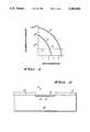
- FIG. 2illustrates a highly enlarged cross-sectional view of a semiconductor wafer 30 having a defect layer 36 in accordance with the present invention.
- Semiconductor wafer 30has a monocrystalline or single crystal lattice structure and a patterned dielectric layer 31 disposed thereon.
- semiconductor wafer 30is a phosphorus doped silicon semiconductor substrate having a resistivity of approximately 42 milliohm-centimeters.
- semiconductor wafer 30may be comprised of other semiconductor substrate materials such as, for example, germanium, gallium arsenide, silicon germanium, indium phosphide, or the like. It shall be further understood that the silicon semiconductor substrate of semiconductor wafer 30 may be either N or P conductivity type having a resistivity in the range of, approximately, 0.001 ohm-centimeter to 100 ohm-centimeters.
- a layer of dielectric material 31is formed over a major surface 32 of semiconductor wafer 30.
- Dielectric material 31is patterned to form a window 33 exposing a portion of major surface 32.
- Dielectric layer 31may be silicon dioxide, silicon nitride, polyimide, or any suitable dielectric material capable of serving as a masking layer. In the zener diode embodiment dielectric layer 31 is silicon dioxide.
- Dielectric layer 31may have a thickness ranging between approximately 0.2 micrometers and 2 micrometers. Methods for forming and patterning a dielectric layer on a semiconductor substrate are well known in the art.
- defect layer 36is indicated in FIG. 2 by a string of x's.
- Defect layer 36may comprise a layer of point defects or an amorphous layer.
- a convenient method for forming defect layer 36is by placing semiconductor wafer 30 having patterned dielectric layer 31 in an ion implant apparatus (not shown) and implanting ions into semiconductor wafer 30. Ion implantation techniques and their disruptive effects on semiconductor substrate crystal lattice structures are well known in the semiconductor processing art.
- Ions implanted into a semiconductor substratedisrupt a crystal lattice structure of that substrate, thereby increasing the number of point defects within the silicon crystal lattice.
- increasing the number of point defects within a semiconductor crystal lattice structureincreases the ease with which a dopant atom travels through the disrupted crystal lattice structure.
- the increase in the number of point defectsresults in an increase in the diffusivity of a dopant in a disrupted region of a semiconductor substrate such as defect layer 36.
- an increased number of point defectsprovides more locations for the dopant to occupy, effectively increasing the solubility of the dopant at a particular temperature.
- the point defect concentrationis determined by the size of the implanted ion and the dose at which the ion is implanted.
- a low implant dose of an ion of a particular sizecreates a layer of point defects wherein increasing the implant dose of that same ion increases the number of point defects.
- an amorphous layeris formed which also results in an increase in the diffusivity and solubility of the dopant.
- larger ionsgenerate a higher density of point defects thereby requiring a lower implant dose to create defect layer 36 than for smaller ions.
- a depth or width of defect layer 36is regulated by the energy used for the ion implant step.
- argon ionsare implanted through window 33 into semiconductor wafer 30 to create defect layer 36, wherein defect layer 36 may be an amorphous layer.
- the argon ionsare implanted at a dose of approximately 5 ⁇ 10 15 ions/cm 2 , an energy of approximately 120 kilo-electron volts. It shall be understood that the dose for the argon ion implant is not a limitation of the present invention. A dose for the argon ion implant may range from approximately 1 ⁇ 10 15 ions per cm 2 to 1 ⁇ 10 16 ions/cm 2 .
- the argon ionsmay be implanted at an implant energy of 40 kilo-electron volts and still produce an amorphous defect layer 36.
- amorphous defect layer 36will have a shallower depth for a 40 kilo-electron volt implant than for the 120 kilo-electron volt implant.
- Other suitable implant materialsinclude boron ions, silicon ions, phosphorous ions, arsenic ions, complex ions such as boron difluoride, and the like.
- silicon dioxide layer 31is patterned to form a guard ring structure for the zener diode.
- the silicon dioxide patternis formed by extending a width of window 33 as shown in FIG. 3. Methods for forming a pattern in silicon dioxide layers such as layer 31 are well known in the art.
- the extension of window 33exposes a portion of major surface 32 adjacent defect layer 36.
- a predeposition layer 37is formed by depositing dopant atoms over patterned silicon dioxide layer 31 the exposed portion of major surface 32 adjacent defect layer 36, and the exposed portion of major surface 32 which is over defect layer 36.
- predeposition layer 37is formed from a gaseous dopant source comprising boron trichloride (BC1 3 ).
- the predeposition stepmay be performed at a temperature ranging between approximately 750° C. and 1,000° C. It shall be understood that the type of predeposition source is not a limitation of the present invention. In other words, the predeposition layer may be deposited using a liquid dopant source or a solid dopant source. Methods for performing the predeposition step are well known in the art.
- the increased number of point defects generated by the ion implant stepincreases the concentration of the dopant or impurity atoms in semiconductor wafer 30 to a level greater than the solid solubility limit.
- concentration of boron atoms in defect layer 36is approximately 2 ⁇ 10 21 atoms/cm 2
- maximum solid solubility limit of boron into a non-disrupted semiconductor wafer at the same temperatureis approximately 5 ⁇ 10 20 atoms/cm 2 .
- the solubility of boronis increased in this region.
- the increase in the solubility and the diffusion rateis not limited to boron, rather a defect layer increases the solubility of other silicon semiconductor dopants such as arsenic, phosphorus, or the like which occurs by creating defect layer 36. It shall be understood that the increase in the solubility and the diffusion rate are not limited to silicon semiconductor wafers but may occur with semiconductor substrates such as, for example, germanium, gallium arsenide, silicon germanium, and indium phosphide.
- FIG. 4illustrates a highly enlarged cross-sectional view of semiconductor wafer 30 after a drive-in or redistribution step in accordance with the present invention.
- a drive-in step in accordance with the zener diode embodiment of the present inventionincludes inserting semiconductor wafer 30, having defect layer 36 and predeposition layer 37 into a diffusion furnace (not shown) set at approximately 750° C.
- predeposition layer 37is removed prior to the drive-in step. Techniques for removing predeposition layer 37 are well known in the art.
- predeposition layer 37is removed in the zener diode embodiment, it shall be understood that removal of predeposition layer 37 is optional.
- silicon dioxide layer 31remains on the semiconductor wafer 30 during the drive-in step.
- the diffusion furnaceis ramped to a temperature of approximately 1200° C. in approximately 60 minutes.
- An ambient atmospherecomprising oxygen and nitrogen is introduced into the diffusion furnace for approximately 55 minutes, then the ambient atmosphere is changed to one comprising hydrogen and oxygen for approximately 120 minutes.
- An annealis performed by changing the ambient atmosphere to one comprising dry oxygen for approximately 120 minutes.
- defect layer 36is annealed or converted into a substantially crystalline structure.
- the diffusion furnaceis ramped down to approximately 750° C. in approximately 115 minutes and semiconductor wafer 30 is removed.
- a drive-in stepmay increase a thickness of an oxide layer such as silicon dioxide layer 31 and oxidizes portions of the semiconductor substrate that may be exposed when using an oxidizing ambient as described.
- oxide layer 31extends across major surface 32.
- the method of driving the dopant into semiconductor wafer 30is not a limitation of the present invention.
- other drive-in methods using oxidizing ambient environments as well as drive-in methods using non-oxidizing ambient environmentsmay be used such as, for example, TEOS in a nitrogen ambient.
- the present inventionallows the simultaneous formation of a guard ring junction 28 and an active junction 29 wherein guard ring junction 28 is at a shallower junction depth than active junction 29. Further, the formation of these two junctions only requires a medium dose of argon rather than two high dose ion implant steps thereby resulting in a monetary and time savings.
- a medium dose of argonranges between approximately 1 ⁇ 10 15 ions/cm 2 and 5 ⁇ 10 15 ions/cm 2 .
- zener diode formationrequires providing metal contacts.
- the silicon dioxide in window 33is removed exposing a portion of major surface 32 and a layer of metal is deposited over the exposed portion of major surface 32.
- a thinning processis performed on a back-side 39 of semiconductor wafer 30 followed by deposition of a metal layer on back-side 39.
- Methods for forming metal contacts to a zener diodeare well known in the art.
- FIG. 5a highly enlarged cross-sectional perspective view of a processing step of a portion of a radio-frequency transistor embodiment is shown.
- the processing stepsare similar to those of the zener diode embodiment.
- the patterning of silicon dioxide layer 41is modified to form an annular window through which an annular defect layer is formed.
- the silicon dioxide present within the annular windowis removed thereby exposing a circular portion of semiconductor wafer 30.
- the two-step doping processis performed wherein the base region 45 is formed.
- An emitter region 46is formed at the center of the circular portion.
- Base and emitter electrodesare formed on surface 43 of semiconductor wafer 30 and a collector electrode (not shown) is formed on the back-side 44 of semiconductor wafer 30.
- Methods for forming emitter regions, and emitter, base, and collector electrodesare well known in the art.
- FIG. 6a highly enlarged cross-sectional view of a portion of a resistor embodiment is shown. Again, the processing steps are similar to those of the zener diode embodiment. However, the patterning of silicon dioxide layer 50 is modified to form a rectangular window in which a defect layer is formed. In the resistor embodiment shown in FIG. 6, a rectangular resistor is shown, however it shall be understood that resistors of other shapes may be formed.
- the two-step doping processis performed forming a doped layer 52.
- the drive-in portion of the two-step doping processforms an oxide in rectangular window thereby forming a single silicon dioxide layer 50.
- Openings 51are formed through silicon dioxide layer 50 and metal contacts (not shown) are made to semiconductor wafer 30 through the openings.
- Methods of forming metal contacts to resistorsare well known in the art. The high doping permitted by the defect layer allows formation of resistors having low resistor values.
- the present inventionprovides a method for modulating the solubility of a semiconductor dopant in a semiconductor wafer.
- a major difference in the doping profileoccurs at the predeposition step wherein the predeposition dopant concentration is initially high and maintains a substantially flat profile in the defect layer rather than the complementary error function profile typical of a predeposition step.
- the predeposition profilebecomes a complementary error function profile.
- the dopant profile of the drive-in stepbecomes a Gaussian profile wherein the concentration of dopant atoms is higher than in a conventional method.
- the present inventionallows a method for achieving a high surface concentration and deeper junction depths without the use of more costly techniques such as multiple ion implants.
- the present inventionis useful in, but not limited to, guard ring formation, providing a lower base resistance and an increased emitter efficiency in bipolar junction transistors, and formation of heavily doped resistors.
- the present inventionprovides a method for simultaneously forming two P-N junctions wherein the two P-N junctions are at different junction depths.
Landscapes
- Physics & Mathematics (AREA)
- Engineering & Computer Science (AREA)
- High Energy & Nuclear Physics (AREA)
- Computer Hardware Design (AREA)
- Condensed Matter Physics & Semiconductors (AREA)
- General Physics & Mathematics (AREA)
- Manufacturing & Machinery (AREA)
- Microelectronics & Electronic Packaging (AREA)
- Power Engineering (AREA)
- Toxicology (AREA)
- Health & Medical Sciences (AREA)
- Spectroscopy & Molecular Physics (AREA)
- Semiconductor Integrated Circuits (AREA)
Abstract
Description
Claims (17)
Priority Applications (1)
| Application Number | Priority Date | Filing Date | Title |
|---|---|---|---|
| US07/996,747US5286660A (en) | 1992-12-24 | 1992-12-24 | Method for doping a semiconductor wafer having a diffusivity enhancement region |
Applications Claiming Priority (1)
| Application Number | Priority Date | Filing Date | Title |
|---|---|---|---|
| US07/996,747US5286660A (en) | 1992-12-24 | 1992-12-24 | Method for doping a semiconductor wafer having a diffusivity enhancement region |
Publications (1)
| Publication Number | Publication Date |
|---|---|
| US5286660Atrue US5286660A (en) | 1994-02-15 |
Family
ID=25543258
Family Applications (1)
| Application Number | Title | Priority Date | Filing Date |
|---|---|---|---|
| US07/996,747Expired - LifetimeUS5286660A (en) | 1992-12-24 | 1992-12-24 | Method for doping a semiconductor wafer having a diffusivity enhancement region |
Country Status (1)
| Country | Link |
|---|---|
| US (1) | US5286660A (en) |
Cited By (14)
| Publication number | Priority date | Publication date | Assignee | Title |
|---|---|---|---|---|
| WO1996032737A1 (en)* | 1995-04-10 | 1996-10-17 | Abb Research Limited | METHOD FOR PRODUCING A SEMICONDUCTOR DEVICE HAVING A SEMICONDUCTOR LAYER OF SiC |
| WO1996032738A1 (en)* | 1995-04-10 | 1996-10-17 | Abb Research Limited | A METHOD FOR INTRODUCTION OF AN IMPURITY DOPANT IN SiC, A SEMICONDUCTOR DEVICE FORMED BY THE METHOD AND A USE OF A HIGHLY DOPED AMORPHOUS LAYER AS A SOURCE FOR DOPANT DIFFUSION INTO SiC |
| US5571731A (en)* | 1993-03-21 | 1996-11-05 | PREMA Pr azisionselektronik GmbH | Procedure for the manufacture of bipolar transistors without epitaxy and with fully implanted base and collector regions which are self-positioning relative to each other |
| EP0769816A1 (en)* | 1995-10-19 | 1997-04-23 | Robert Bosch Gmbh | High breakdown voltage PM junction and method for making it |
| US5712176A (en)* | 1995-06-30 | 1998-01-27 | Lucent Technologies Inc. | Doping of silicon layers |
| US5759904A (en)* | 1996-11-06 | 1998-06-02 | Southwest Research Institute | Suppression of transient enhanced diffusion in ion implanted silicon |
| EP0938130A3 (en)* | 1998-02-12 | 1999-10-20 | Lucent Technologies Inc. | A process for fabricating a device with shallow junctions |
| US6077734A (en)* | 1996-12-20 | 2000-06-20 | Hyundai Electronics Industries, Co., Ltd. | Method of fabricating semiconductor device with extremely shallow junction |
| US20030096464A1 (en)* | 2001-11-21 | 2003-05-22 | Frederic Lanois | Method for forming a schottky diode on a silicon carbide substrate |
| US6617228B2 (en)* | 2000-09-05 | 2003-09-09 | The Regents Of The University Of California | Semiconductor material and method for enhancing solubility of a dopant therein |
| DE102004029945A1 (en)* | 2004-06-21 | 2006-01-05 | Infineon Technologies Ag | Production of a doped zone in the region of a surface of a semiconductor layer used in the production of MOSFETs comprises forming an amorphous semiconductor layer in the region of the semiconductor layer and further processing |
| US20080023795A1 (en)* | 2005-05-20 | 2008-01-31 | Toyota Jidosha Kabushiki Kaisha | Semiconductor devices and method of manufacturing them |
| JP2014138173A (en)* | 2013-01-18 | 2014-07-28 | Shi Exaination & Inspection Ltd | Method of manufacturing semiconductor device, and substrate processing system |
| DE102017118864A1 (en)* | 2017-08-18 | 2019-02-21 | Infineon Technologies Austria Ag | power diode |
Citations (2)
| Publication number | Priority date | Publication date | Assignee | Title |
|---|---|---|---|---|
| US3796929A (en)* | 1970-12-09 | 1974-03-12 | Philips Nv | Junction isolated integrated circuit resistor with crystal damage near isolation junction |
| US4216030A (en)* | 1976-06-22 | 1980-08-05 | Siemens Aktiengesellschaft | Process for the production of a semiconductor component with at least two zones which form a pn-junction and possess differing conductivity types |
- 1992
- 1992-12-24USUS07/996,747patent/US5286660A/ennot_activeExpired - Lifetime
Patent Citations (2)
| Publication number | Priority date | Publication date | Assignee | Title |
|---|---|---|---|---|
| US3796929A (en)* | 1970-12-09 | 1974-03-12 | Philips Nv | Junction isolated integrated circuit resistor with crystal damage near isolation junction |
| US4216030A (en)* | 1976-06-22 | 1980-08-05 | Siemens Aktiengesellschaft | Process for the production of a semiconductor component with at least two zones which form a pn-junction and possess differing conductivity types |
Cited By (24)
| Publication number | Priority date | Publication date | Assignee | Title |
|---|---|---|---|---|
| US5571731A (en)* | 1993-03-21 | 1996-11-05 | PREMA Pr azisionselektronik GmbH | Procedure for the manufacture of bipolar transistors without epitaxy and with fully implanted base and collector regions which are self-positioning relative to each other |
| US5851908A (en)* | 1995-04-10 | 1998-12-22 | Abb Research Ltd. | Method for introduction of an impurity dopant in SiC, a semiconductor device formed by the method and a use of highly doped amorphous layer as a source for dopant diffusion into SiC |
| WO1996032738A1 (en)* | 1995-04-10 | 1996-10-17 | Abb Research Limited | A METHOD FOR INTRODUCTION OF AN IMPURITY DOPANT IN SiC, A SEMICONDUCTOR DEVICE FORMED BY THE METHOD AND A USE OF A HIGHLY DOPED AMORPHOUS LAYER AS A SOURCE FOR DOPANT DIFFUSION INTO SiC |
| WO1996032737A1 (en)* | 1995-04-10 | 1996-10-17 | Abb Research Limited | METHOD FOR PRODUCING A SEMICONDUCTOR DEVICE HAVING A SEMICONDUCTOR LAYER OF SiC |
| US6096627A (en)* | 1995-04-10 | 2000-08-01 | Abb Research Ltd. | Method for introduction of an impurity dopant in SiC, a semiconductor device formed by the method and a use of a highly doped amorphous layer as a source for dopant diffusion into SiC |
| US5804482A (en)* | 1995-04-10 | 1998-09-08 | Abb Research Ltd. | Method for producing a semiconductor device having a semiconductor layer of SiC |
| US5712176A (en)* | 1995-06-30 | 1998-01-27 | Lucent Technologies Inc. | Doping of silicon layers |
| EP0769816A1 (en)* | 1995-10-19 | 1997-04-23 | Robert Bosch Gmbh | High breakdown voltage PM junction and method for making it |
| US5759904A (en)* | 1996-11-06 | 1998-06-02 | Southwest Research Institute | Suppression of transient enhanced diffusion in ion implanted silicon |
| US6077734A (en)* | 1996-12-20 | 2000-06-20 | Hyundai Electronics Industries, Co., Ltd. | Method of fabricating semiconductor device with extremely shallow junction |
| EP0938130A3 (en)* | 1998-02-12 | 1999-10-20 | Lucent Technologies Inc. | A process for fabricating a device with shallow junctions |
| US6136673A (en)* | 1998-02-12 | 2000-10-24 | Lucent Technologies Inc. | Process utilizing selective TED effect when forming devices with shallow junctions |
| US6617228B2 (en)* | 2000-09-05 | 2003-09-09 | The Regents Of The University Of California | Semiconductor material and method for enhancing solubility of a dopant therein |
| US20030096464A1 (en)* | 2001-11-21 | 2003-05-22 | Frederic Lanois | Method for forming a schottky diode on a silicon carbide substrate |
| US7101739B2 (en)* | 2001-11-21 | 2006-09-05 | Stmicroelectronics S.A. | Method for forming a schottky diode on a silicon carbide substrate |
| DE102004029945A1 (en)* | 2004-06-21 | 2006-01-05 | Infineon Technologies Ag | Production of a doped zone in the region of a surface of a semiconductor layer used in the production of MOSFETs comprises forming an amorphous semiconductor layer in the region of the semiconductor layer and further processing |
| DE102004029945B4 (en)* | 2004-06-21 | 2008-01-17 | Infineon Technologies Ag | Method for producing a near-surface doped zone in a semiconductor body |
| US20080023795A1 (en)* | 2005-05-20 | 2008-01-31 | Toyota Jidosha Kabushiki Kaisha | Semiconductor devices and method of manufacturing them |
| US7569914B2 (en)* | 2005-05-20 | 2009-08-04 | Toyota Jidosha Kabushiki Kaisha | Semiconductor devices and method of manufacturing them |
| JP2014138173A (en)* | 2013-01-18 | 2014-07-28 | Shi Exaination & Inspection Ltd | Method of manufacturing semiconductor device, and substrate processing system |
| DE102017118864A1 (en)* | 2017-08-18 | 2019-02-21 | Infineon Technologies Austria Ag | power diode |
| US10978596B2 (en) | 2017-08-18 | 2021-04-13 | Infineon Technologies Austria Ag | Power diode and method of manufacturing a power diode |
| US11695083B2 (en) | 2017-08-18 | 2023-07-04 | Infineon Technologies Austria Ag | Power diode and method of manufacturing a power diode |
| US12211945B2 (en) | 2017-08-18 | 2025-01-28 | Infineon Technologies Austria Ag | Power diode and method of manufacturing a power diode |
Similar Documents
| Publication | Publication Date | Title |
|---|---|---|
| US4063967A (en) | Method of producing a doped zone of one conductivity type in a semiconductor body utilizing an ion-implanted polycrystalline dopant source | |
| US4495010A (en) | Method for manufacturing fast bipolar transistors | |
| US4357622A (en) | Complementary transistor structure | |
| US5286660A (en) | Method for doping a semiconductor wafer having a diffusivity enhancement region | |
| US4521441A (en) | Plasma enhanced diffusion process | |
| EP0033495B1 (en) | Process for fabricating a high speed bipolar transistor | |
| WO1985002940A1 (en) | Method for making a conductive silicon substrate and a semiconductor device formed therein | |
| US4295898A (en) | Method of making isolated semiconductor devices utilizing ion-implantation of aluminum and heat treating | |
| US5137838A (en) | Method of fabricating P-buried layers for PNP devices | |
| EP0094482A2 (en) | Fabrication process for a shallow emitter, narrow intrinsic base transistor | |
| US4373252A (en) | Method for manufacturing a semiconductor structure having reduced lateral spacing between buried regions | |
| US3745070A (en) | Method of manufacturing semiconductor devices | |
| GB1415500A (en) | Semiconductor devices | |
| US3943555A (en) | SOS Bipolar transistor | |
| US4502894A (en) | Method of fabricating polycrystalline silicon resistors in integrated circuit structures using outdiffusion | |
| US5310711A (en) | Method of forming doped shallow electrical junctions | |
| US4717687A (en) | Method for providing buried layer delineation | |
| US3982967A (en) | Method of proton-enhanced diffusion for simultaneously forming integrated circuit regions of varying depths | |
| JPS5879762A (en) | Submicron bipolar transistor and method of producing same | |
| US4898837A (en) | Method of fabricating a semiconductor integrated circuit | |
| US3974560A (en) | Method of making a bipolar transistor | |
| US4758537A (en) | Lateral subsurface zener diode making process | |
| EP0417737B1 (en) | Method of manufacturing a semiconductor device using ion implantation | |
| EP0219243A2 (en) | Process of manufacturing a bipolar transistor | |
| US3770516A (en) | Monolithic integrated circuits |
Legal Events
| Date | Code | Title | Description |
|---|---|---|---|
| AS | Assignment | Owner name:MOTOROLA INC., ILLINOIS Free format text:ASSIGNMENT OF ASSIGNORS INTEREST;ASSIGNORS:CHIOU, HERNG-DER;EHLENBERGER, GARY G.;FUCHS, EARL D.;REEL/FRAME:007292/0897 Effective date:19921218 | |
| STCF | Information on status: patent grant | Free format text:PATENTED CASE | |
| CC | Certificate of correction | ||
| FPAY | Fee payment | Year of fee payment:4 | |
| AS | Assignment | Owner name:CHASE MANHATTAN BANK, THE, AS COLLATERAL AGENT, NE Free format text:SECURITY AGREEMENT;ASSIGNOR:SEMICONDUCTOR COMPONENTS INDUSTRIES, LLC;REEL/FRAME:010281/0057 Effective date:19990804 | |
| FEPP | Fee payment procedure | Free format text:PAYOR NUMBER ASSIGNED (ORIGINAL EVENT CODE: ASPN); ENTITY STATUS OF PATENT OWNER: LARGE ENTITY | |
| AS | Assignment | Owner name:SEMICONDUCTOR COMPONENTS INDUSTRIES, LLC, ARIZONA Free format text:ASSIGNMENT OF ASSIGNORS INTEREST;ASSIGNOR:MOTOROLA, INC.;REEL/FRAME:010776/0122 Effective date:20000414 | |
| FPAY | Fee payment | Year of fee payment:8 | |
| AS | Assignment | Owner name:JPMORGAN CHASE BANK, AS COLLATERAL AGENT, NEW YORK Free format text:SUPPLEMENT TO SECURITY AGREEMENT;ASSIGNORS:SEMICONDUCTOR COMPONENTS INDUSTRIES, LLC;SEMICONDUCTOR COMPONENTS OF RHODE ISLAND, INC.;REEL/FRAME:012991/0180 Effective date:20020505 | |
| AS | Assignment | Owner name:WELLS FARGO BANK MINNESOTA, NATIONAL ASSOCIATION, Free format text:SECURITY AGREEMENT;ASSIGNORS:SEMICONDUCTOR COMPONENTS INDUSTRIES, LLC;SEMICONDUCTOR COMPONENTS INDUSTRIES OF RHODE ISLAND, INC.;REEL/FRAME:012958/0638 Effective date:20020506 | |
| AS | Assignment | Owner name:JPMORGAN CHASE BANK, NEW YORK Free format text:SECURITY INTEREST;ASSIGNOR:SEMICONDUCTOR COMPONENTS INDUSTRIES, LLC;REEL/FRAME:014007/0239 Effective date:20030303 | |
| FPAY | Fee payment | Year of fee payment:12 | |
| AS | Assignment | Owner name:SEMICONDUCTOR COMPONENTS INDUSTRIES, LLC, ARIZONA Free format text:RELEASE BY SECURED PARTY;ASSIGNOR:WELLS FARGO BANK MINNESOTA, NATIONAL ASSOCIATION, AS COLLATERAL AGENT;REEL/FRAME:038543/0039 Effective date:20050217 |