US5285779A - Method and apparatus for a cardiac defibrillator high voltage charging circuit - Google Patents
Method and apparatus for a cardiac defibrillator high voltage charging circuitDownload PDFInfo
- Publication number
- US5285779A US5285779AUS07/858,808US85880892AUS5285779AUS 5285779 AUS5285779 AUS 5285779AUS 85880892 AUS85880892 AUS 85880892AUS 5285779 AUS5285779 AUS 5285779A
- Authority
- US
- United States
- Prior art keywords
- transformer
- battery
- voltage
- output
- energy
- Prior art date
- Legal status (The legal status is an assumption and is not a legal conclusion. Google has not performed a legal analysis and makes no representation as to the accuracy of the status listed.)
- Expired - Fee Related
Links
- 230000000747cardiac effectEffects0.000titleclaimsdescription26
- 238000000034methodMethods0.000titleclaimsdescription10
- 238000004804windingMethods0.000claimsabstractdescription131
- 239000003990capacitorSubstances0.000claimsabstractdescription115
- 238000004146energy storageMethods0.000claimsdescription10
- 238000007599dischargingMethods0.000claimsdescription6
- 238000012546transferMethods0.000claimsdescription2
- 230000008878couplingEffects0.000claims5
- 238000010168coupling processMethods0.000claims5
- 238000005859coupling reactionMethods0.000claims5
- 239000006185dispersionSubstances0.000claims1
- 238000012986modificationMethods0.000claims1
- 230000004048modificationEffects0.000claims1
- 230000001131transforming effectEffects0.000claims1
- 230000009977dual effectEffects0.000description17
- 230000003750conditioning effectEffects0.000description16
- 238000010586diagramMethods0.000description12
- 230000002441reversible effectEffects0.000description8
- 230000015556catabolic processEffects0.000description3
- 238000012544monitoring processMethods0.000description3
- 230000004888barrier functionEffects0.000description2
- 230000001143conditioned effectEffects0.000description2
- 230000009849deactivationEffects0.000description2
- 230000007423decreaseEffects0.000description2
- 230000000694effectsEffects0.000description2
- 230000005669field effectEffects0.000description2
- 230000000977initiatory effectEffects0.000description2
- 238000002955isolationMethods0.000description2
- OKTJSMMVPCPJKN-UHFFFAOYSA-NCarbonChemical compound[C]OKTJSMMVPCPJKN-UHFFFAOYSA-N0.000description1
- RYGMFSIKBFXOCR-UHFFFAOYSA-NCopperChemical compound[Cu]RYGMFSIKBFXOCR-UHFFFAOYSA-N0.000description1
- 230000004913activationEffects0.000description1
- 230000002411adverseEffects0.000description1
- 238000013459approachMethods0.000description1
- 238000013194cardioversionMethods0.000description1
- 230000008859changeEffects0.000description1
- 238000001816coolingMethods0.000description1
- 229910052802copperInorganic materials0.000description1
- 239000010949copperSubstances0.000description1
- 238000013461designMethods0.000description1
- 230000004907fluxEffects0.000description1
- 230000010355oscillationEffects0.000description1
- 238000013021overheatingMethods0.000description1
- 230000003071parasitic effectEffects0.000description1
- 230000008569processEffects0.000description1
- 230000001629suppressionEffects0.000description1
- 230000001360synchronised effectEffects0.000description1
- 230000001052transient effectEffects0.000description1
- 230000001960triggered effectEffects0.000description1
Images


Classifications
- A—HUMAN NECESSITIES
- A61—MEDICAL OR VETERINARY SCIENCE; HYGIENE
- A61N—ELECTROTHERAPY; MAGNETOTHERAPY; RADIATION THERAPY; ULTRASOUND THERAPY
- A61N1/00—Electrotherapy; Circuits therefor
- A61N1/18—Applying electric currents by contact electrodes
- A61N1/32—Applying electric currents by contact electrodes alternating or intermittent currents
- A61N1/38—Applying electric currents by contact electrodes alternating or intermittent currents for producing shock effects
- A61N1/39—Heart defibrillators
- A61N1/3925—Monitoring; Protecting
- A—HUMAN NECESSITIES
- A61—MEDICAL OR VETERINARY SCIENCE; HYGIENE
- A61N—ELECTROTHERAPY; MAGNETOTHERAPY; RADIATION THERAPY; ULTRASOUND THERAPY
- A61N1/00—Electrotherapy; Circuits therefor
- A61N1/18—Applying electric currents by contact electrodes
- A61N1/32—Applying electric currents by contact electrodes alternating or intermittent currents
- A61N1/38—Applying electric currents by contact electrodes alternating or intermittent currents for producing shock effects
- A61N1/39—Heart defibrillators
- A61N1/3975—Power supply
- A61N1/3981—High voltage charging circuitry
Definitions
- This inventionrelates to cardiac defibrillators and more particularly to defibrillators powered from alternate power sources.
- Cardiac defibrillatorsgenerate a high voltage output that is discharged from a capacitor into a patient to perform either defibrillation or synchronized cardioversion.
- the life of a patientmay depend upon a defibrillator's reliability and whether it can generate sufficient energy in a limited amount of time.
- a defibrillator charger circuitwhich operates from a single power supply, is described in Hewlett-Packard operating manual, 43100A Defibrillator/Monitor and Recorder, May 1988, Part No. 43100-91909 and is incorporated by reference.
- the defibrillatorIt is desirable that the defibrillator have the capacity to operate in different situations; for example, in a hospital emergency room or in remote locations such as an ambulance. It is therefore necessary that the defibrillator's high voltage charging transformer be able to efficiency receive and transform power from DC power supplies with different output characteristics.
- the transformershould typically be capable of receiving power from either an AC-to-DC converter (e.g. for 120 volt AC "plug in" type source) or from a DC battery.
- One object of the present inventionis to energize a cardiac defibrillator from multiple power supplies with reliable switching between supplies.
- a second objectis to increase the fault tolerance of a cardiac defibrillator energized by alternate power supplies when voltage or current conditions of one of the supplies is outside normal operating ranges.
- Another objectis to reduce the charge time of a cardiac defibrillator by single or multiple power supplies in coordination with the power supply output conditions.
- Yet another objectis to reduce charge failures in cardiac defibrillators by providing automatic on-line battery recharging.
- the inventionis a quick-charging, high-reliability cardiac defibrillator that uses a dual primary high voltage transformer to energize a high voltage storage and discharge capacitor from at least two DC power supplies.
- Poweris primarily supplied to the transformer by a battery supply; however, depending upon the battery output, a second DC power supply can be activated.
- the power suppliesoperate separately or together to supply energy to the transformer.
- the transformeroperates in a fly-back mode whereby current is not allowed to pass through the secondary winding until the power supplies have deactivated. Upon deactivation of the power supplies, current begins to flow through the secondary winding, discharging the energy stored in the transformer into the high voltage storage capacitor. The energy in the storage capacitor is then discharged into a patient.
- the dual primary winding high voltage transformeraccepts the internal battery supply on a first primary winding and the output from an AC-to-DC converter on a secondary primary winding. Providing two primary windings allows the output characteristics for each power supply to be individually matched. Thus, the transformer allows fast, high current charging from the battery, and slower low current charging from the AC-to-DC converter. Since each power supply is separately coupled to the transformer by a primary winding, fault conditions occurring on either power supply are isolated.
- the AC power source feeding the AC-to-DC converteris detachable, allowing the defibrillator to be operated remotely. With the converter detached, the storage capacitor is charged solely from the internal battery. The battery is not allowed to provide current to the transformer if the battery output voltage would drop below the level necessary to maintain normal defibrillator operation.
- additional circuitrymonitors the output voltage level of both power supplies. Accordingly, if the battery has a sufficient output voltage, the output from the AC-to-DC converter is restricted in supplying energy to the transformer. When the battery has a low output voltage, however, output from the AC-to-DC power supply contributes more energy to the charging of the transformer. If the battery is severely discharged, power from the AC-to-DC converter output is used to recharge the battery.
- the power suppliesare activated with a pulse width modulated signal.
- Each modulation cycleincreases the amount of energy in the stage capacitor.
- the number of cycles and the duration of each cycleare controlled by external defibrillator control circuitry.
- the time required to discharge the transformeris dependant upon the amount of energy already stored in the capacitor. Therefore, the power supplies are activated at a variable rate that depends upon the time required for energy to transfer from the transformer to the storage capacitor.
- the pulse width modulatoris fed parametric information from monitoring circuits on both the primary and secondary sides of the transformer. The modulator in turn disables the power supplies if excessive current or voltage levels occur in the defibrillator system.
- the secondary coil of the transformeris coupled by a diode to the storage capacitor.
- the diodeUpon activation of power on the primary side of the transformer, the diode becomes reverse biased. This prevents current from passing through the secondary winding, causing the transformer to store energy.
- the voltage on the secondary windingincreases, forward biasing the diode.
- the transformerthen discharges energy into the storage capacitor. The voltage across the storage capacitor is monitored and charging cycles are repeated until the storage capacitor reaches a preset voltage level.
- the dual primary, high voltage transformer and the associated charging circuitryprovide a low cost, reliable means for quickly charging a cardiac defibrillator.
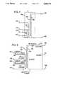
- FIG. 1is a block diagram for a prior art cardiac defibrillator charging circuit energized from a single power supply.
- FIG. 2is a block diagram of a cardiac defibrillator charging circuit energized from a battery and an AC/DC power supply in accordance with the invention.
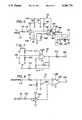
- FIG. 3is a detailed circuit diagram of the dual primary transformer/rectifier, low current switch/switch driver, high current switch, primary current sense, and power disable in FIG. 2.
- FIG. 4is a detailed circuit diagram of the transformer in FIG. 3.
- FIG. 5is a parametric representation of the transformer in FIG. 3.
- FIG. 6is a detailed circuit diagram of the optically coupled capacitor current sense circuitry in FIG. 2.
- FIG. 7is a detailed circuit diagram of the differential amplified capacitor voltage metering circuit in FIG. 2.
- FIG. 8is a detailed schematic diagram of the low voltage sense circuit in FIG. 2.
- FIG. 1shows the general arrangement of the charging circuit for the Hewlett-Packard 43100A Defibrillator/Monitor with Recorder mentioned above.
- a power conditioning circuit 18receives a power supply input. The output of power conditioning circuit 18 is coupled to the primary winding of transformer/rectifier circuit 32.
- a conventional defibrillator control board(not shown) supplies control signals: safety relay drive (SFRLYDR), charge enable (CHGEN), and charge rate (CHRATE), to the defibrillator charging circuit in FIG. 1.
- SFRLYDRsafety relay drive
- CHGENcharge enable
- CHRATEcharge rate
- a safety circuit 30is coupled across an energy storage capacitor (not shown) and receives SFRLYDR.
- a charge disable circuit 20is coupled at the input to the SFRLYDR and CHGEN signals, and has an output to the shutdown pin of a pulse width modulator (PWM) 28.
- PWMpulse width modulator
- a charge rate ramp generator circuit 22is driven by a voltage output from PWM 28 and has an output coupled to the oscillator/comparator input of PWM 28.
- a charge rate threshold generator circuit 24receives the CHRATE signal at its input and its output is coupled to the inverting comparator input on PWN 28.
- a low battery sense circuit 26is coupled to the input from the power supply, and has an output coupled to the inverting comparator input of PWM 28.
- PWM 28is a Unitrode 3524A, pulse width modulator.
- the modulatorreceives input signals from charge disable circuit 20, charge rate ramp generator circuit 22, charge rate threshold generator circuit 24, low battery sense circuit 26, a primary current sense circuit 36, a capacitor current sense circuit 38, and a capacitor voltage metering circuit 40.
- the output of PWM 28drives a high current switch 34.
- Transformer/rectifier circuit 32is coupled at a first terminal of a primary winding to the output of power conditioning circuit 18 and is coupled at a second terminal of the primary winding to high current switch 34.
- the output of high current switch 34feeds primary current sense 36.
- the secondary winding of transformer/rectifier circuit 32is a high voltage output coupled to an energy storage capacitor (not shown), monitoring signal outputs coupled to capacitor voltage metering circuit 40 and capacitor current sense circuit 38.
- the defibrillator charger circuit in FIG. 1is a variable frequency, fly-back DC-DC high voltage charging circuit that operates from a single power supply.
- a batterysupplies a DC voltage to power conditioning circuit 18. If the battery produces a large current surge, power conditioning circuit 18 provides bypassing for the defibrillator charging circuit. If there is no current surge, the battery voltage is fed directly into the primary winding of transformer/rectifier circuit 32. The voltage from the battery is stepped up by the transformer and eventually discharged into the energy storage capacitor. The energy storage capacitor, when charged sufficiently, is then discharged, through additional defibrillator control circuitry (not shown), into a patient.
- the secondary winding of the transformeris coupled by a diode (inside transformer/rectifier circuit 32), to the storage capacitor (see FIG. 3).
- the diodecauses the transformer to operate in a fly-back mode, described below in the discussion of FIG. 3.
- a fly-back modethe transformer stores energy when the battery is charging the transformer primary winding.
- the transformerdischarges stored energy into the storage capacitor.
- the batteryrecharges the transformer. This process is repeated until the storage capacitor is charged to a level set by the defibrillator control board.
- Safety circuit 30provides a switchable shunt resistor for discharging the storage capacitor. The shunt resistor is typically connected across the storage capacitor when power is disconnected from the defibrillator charging circuit.
- the pulse width modulatoris controlled by charge disable 20, charge rate ramp generator 22, charge rate threshold generator 24, low battery sense 26, primary current sense 36, capacitor current sense 38, and capacitor voltage metering 40.
- the external defibrillator control boarddrives CHGEN and SFRLYDR low. This causes charge enable 20 to generate a high impedance output, enabling the shutdown pin on PWM 28. For the output of PWN 28 to go high, its shutdown pin must be enabled and the output voltage of charge rate ramp generator 22 must be less than the voltage output of charge rate threshold generator 24.
- the charge rate ramp generator 22supplies an output voltage to PWM 28 that increases approximately linearly with time. This voltage is compared in PWM 28 with the output of charge rate threshold generator 24. As the output voltage of charge rate ramp generator 22 increases, but is still less than the charge rate threshold generator output, the output of PWM 28 goes high, turning on high current switch 34.
- the batteryWhen the high current switch is turned on, the battery begins charging the transformer through the primary winding.
- PWM 28To increase the amount of time PWM 28 remains on, the voltage level of CHRATE signal is increased by the defibrillator control board. The higher voltage requires more time for the output of charge rate ramp generator 22 to reach the threshold generator output voltage. Thus, PWM 28 remains active longer, allowing the power supply to provide more energy to the transformer/rectifier circuit.
- PWM 28remains active longer, allowing the power supply to provide more energy to the transformer/rectifier circuit.
- the voltage of the CHRATE signalis reduced. This produces a lower voltage at the output of charge rate threshold genertor 24, allowing the charge rate ramp generator to reach the charge rate threshold voltage in a shorter amount of time. The battery is thereby activated for a shorter time, transferring less energy into the storage capacitor.
- a voltage comparator inside PWM 28disables the modulator output, and resets the output of charge rate ramp generator 22 to zero volts.
- the output of charge rate ramp generator 22immediately begins increasing, starting another charging cycle. If no alternative inputs to PWM 28 go into a disable state, the output of PWM 32 again goes high and the transformer is again charged.
- Charge rate threshold generator 24also disables PWM 28 when the CHRATE signal is at zero volts (e.g. cable from the defibrillator control board to the defibrillator charger disconnected). If the CHRATE signal is a positive voltage, however, the output of charge rate threshold generator 24 goes into a high impedance state, removing the disable signal from PWM 28.
- the CHRATE signalis at zero volts (e.g. cable from the defibrillator control board to the defibrillator charger disconnected). If the CHRATE signal is a positive voltage, however, the output of charge rate threshold generator 24 goes into a high impedance state, removing the disable signal from PWM 28.
- the charge rate ramp generator output voltagerises at a slower rate for lower battery voltage outputs. This partially compensates for otherwise slowed charging under low battery output conditions.
- Capacitor current sense 38monitors the secondary side current, keeping PWM 28 off when the transformer is discharging energy into the storage capacitor. The capacitor current sense allows the modulator to begin another charging cycle when secondary current no longer passes from the transformer to the storage capacitor. Thus, the defibrillator charging circuit operates at variable frequencies depending on the rate in which energy is transferred from the transformer to the storage capacitor.
- Capacitor voltage metering circuit 40monitors the voltage across the storage capacitor. The capacitor voltage is scaled, then fed back to PWM 28. When the storage capacitor voltage is excessive, PWM 28 is disabled to prevent any further charging of the capacitor.
- the scaled storage capacitor voltageis also fed back to the defibrillator control board.
- the control boardallows the charging circuit to continue supplying energy to the transformer (e.g. keep both CHGEN and SFRLYDR low and CHRATE high) until the storage capacitor is fully charged.
- Low battery sense 26disables PWM 28 if the battery voltage is too low and primary current sense 36 disables PWM 28 if excessive current passes through high current switch 34.
- the main problem with the defibrillator charging circuit in FIG. 1is that there is only one path for supplying power to the transformer. For example, to change power sources, either the battery must be physically disconnected so the second supply can be connected, or switching circuitry must be provided that disconnects the battery and reconnects the output from a second power supply (e.g., an AC-to-DC converter) to power conditioning circuit 18.
- a second power supplye.g., an AC-to-DC converter
- One problem with the latter approachis providing reliable switching circuitry that also provides low energy loss for the high current drawn by transformer/rectifier circuit 32. This typically requires a high current relay, or a field effect transisitor with a very low drain/source resistance. Both of these parts are expensive and require additional drive logic.
- the AC-to-DC converteris not capable of supplying as much peak current as the battery, so if transformer/rectifier circuit 32 is optimized for the battery it is not optimized for the AC-to-DC converter.
- FIG. 2shows the general arrangement for a preferred embodiment of a dual power supply defibrillator charging circuit in accordance with the invention.
- charge enable 20, charge rate ramp generator 22, charge rate threshold generator 24, high current switch 34, and primary current sense 36operate substantially the same as described in FIG. 1 and so as identified by like reference numerals.
- Safety circuit 30also operates substantially the same as described in FIG. 1, only it is now driven by open safety relay signal (OPNSFRLY) from the above-described defibrillator control board (not shown).
- OPNSFRLY signalis the inverted value of signal SFRLYDR.
- Power disable/conditioning circuit 58performs substantially the same circuit bypassing function as power conditioning circuit 18 in FIG. 1, but now provides circuit bypassing concurrently for both a DC battery 52, and an AC-to-DC converter 50. Power disable/conditioning circuit 58 also provides additional disable circuitry illustrated in FIG. 3.
- a dual primary, transformer/rectifier circuit 62has two primary windings instead of the single primary used in circuit 32 of FIG. 1.
- the first primary windingis connected to the VDC output from power disable/conditioning circuit 58.
- the second primary windingis connected to the Vbattery output from power disable/conditioning circuit 58.
- the secondary winding of the transformeris connected to an optocoupled capacitor current sense circuit 64, safety circuit 30, a differential amplified capacitor voltage metering circuit 66, and an energy storage capacitor 68.
- Transformer 62provides an isolation barrier between the power supply circuitry coupled to the primary winding and the charge capacitor and monitoring circuitry coupled to the secondary winding. This isolation barrier protects the patient and operator from high voltages on the secondary winding of transformer 62 and from the energy stored on energy storage capacitor 68.
- a low current switch in low current switch/switch driver circuit 60is coupled to a low current primary winding on dual primary transformer/rectifier circuit 62.
- a driver circuit in low current switch/switch driver circuit 60drives both the low current switch and high current switch 34.
- High current switch 34is coupled to a high current primary winding on dual primary transformer/rectifier circuit 62.
- FIG. 3provides a more detailed diagram of dual primary transformer/rectifier circuit 62, low current switch/switch driver circuit 60, high current switch 34, primary current sense 36, and the disable circuitry of power disable/conditioning circuit 58.
- Optocoupled capacitor current sense 64performs substantially the same function as capacitor current sense 38 in FIG. 1. Changes to the circuits involve optocoupling between the input and output. The circuit is shown in detail in FIG. 6.
- Differential amplifier capacitor voltage metering circuit 66performs substantially the same function as capacitor voltage metering circuit 40 in FIG. 1. The output, however, is now the scaled voltage difference across the secondary of the dual primary transformer. This circuit is shown in detail in FIG. 7.
- a low voltage sense circuit 56is similar to low battery sense 26 in FIG. 1 except low voltage sense circuit 56 now receives an additional defibrillator control signal, AC ON charger (ACONCH).
- ACONCHAC ON charger
- the ACONCH signalgoes high when the DC supply voltage VDC is connected to the defibrillator charging circuit and goes low when VDC is disconnected.
- Low voltage sense 56is illustrated in detail in FIG. 8.
- FIG. 3is a detailed circuit diagram of low current switch circuit 60A and switch driver circuit 60B, the disable circuitry of power disable conditioning circuit 58, high current switch 34, primary current sense 36, and dual primary transformer/rectifier circuit 62 in FIG. 1.
- Dashed box 60Bidentifies the switch driver circuit in low current switch/switch driver circuit 60 and dashed box 60A identifies the low current switch of low current switch/switch drive circuit 60 (FIG. 2).
- Dashed box 36surrounds the primary current sense in FIG. 2 and dashed box 34 surrounds the high current switch in FIG. 2.
- the disable circuitry of the power disable/conditioning circuit of FIG. 2is surrounded by dashed box 58 and the dual primary transformer/rectifier circuit of FIG. 2 is surrounded by dashed box 62.
- Input terminal 74 of circuit 60Bis coupled to the output of PWM 28 (FIG. 2) and to the first terminals of resistors 78 and 76.
- the second terminal of resistor 78is coupled to output terminal 80 and to ground by resistor 82.
- the second terminal of resistor 76is connected to the anode of diode 84 and to the base of transistor 86.
- the cathode of diode 84is connected to the emitter of transistor 86, the cathode of Zener diode 88, and to the first terminals of resistors 90 and 92 in high current switch 34 and resistor 106 in circuit 60A.
- the collector of transistor 86 and the anode of Zener diode 88are connected to ground.
- the second terminal of resistor 90is coupled to the gate of field effect transistor (FET) 102 and the second terminal of resistor 92 is coupled to the gate of FET 104.
- the source of FET 102is connected to the source of FET 104, and to the first terminal of resistor 94 and the first terminal of resistor 96 in current sense circuit 36.
- the second terminal of resistor 96is connected to output terminal 100 and the first terminal of capacitor 98.
- the second terminal of resistor 94 and the second terminal of capacitor 98are coupled to ground.
- the drain of transistor 102is coupled to the drain of transistor 104, the cathode of Zener diode 106 and the dotted terminal of the high current primary winding 144 of transformer 126 in circuit 62.
- the anode of Zener diode 106is coupled to ground.
- the gate of FET 110is coupled to the second terminal of resistor 106 and the source of FET 110 is coupled to ground.
- Zener diode 108is coupled at the anode to ground and coupled at the cathode to the drain of transistor 110 and to the dotted terminal of a low current primary winding 142 of transformer 126.
- Power disable/conditioning circuit 58(FIG. 2) has an input terminal 112 which receives supply voltage VDC (conditioned AC-to-DC converter output) and an input terminal 118 which receives the battery output voltage Vbattery (conditioned battery output).
- VDCconditioned AC-to-DC converter output
- Vbatteryconditioned battery output
- the supply voltageis coupled through a diode 114 to the non-dotted terminal of the low current primary winding 142 of transformer 126.
- a capacitor 116 connected to the cathode of diode 114is coupled to ground to filter VDC.
- the battery voltage input at terminal 118is coupled through fuse 120 to the non-dotted terminal of the high current primary winding 144 of transformer 126.
- Capacitor 122 and 124capacitively couple Vbattery to ground.
- the secondary winding 148 of transformer 126has a diode 128 connected at its dotted terminal and a diode 132 connected at its non-dotted terminal so as to conduct current unidirectionally from terminal 72 toward terminal 70.
- Zener diode 130is coupled between diode 128 and terminal 70 and blocks current until its reverse bias avalanche voltage is exceeded at the anode.
- FIG. 4is a detailed schematic of transformer 126 in FIG. 3.
- Low current primary winding 142is coupled at the dotted terminal to the drain of FET 110 and coupled at the non-dotted terminal to the cathode of diode 114.
- High current primary winding 144is coupled at the dotted terminal to the drain of FETs 102 and 104, and is coupled at the non-dotted terminal to Vbattery.
- the secondary winding of the transformeris coupled at the dotted terminal to the anode of diode 128 and is connected at the non-dotted terminal to the cathode of diode 132.
- Primary winding 144 to primary winding 1421:1.8.
- the number of turns and the associated parametric data selected for the primary windings 142 and 144 of the transformer 126are selected to match the output characteristics of the power supplies VDC and Vbattery, respectively. Matching the output characteristics of each power supply with the input characteristics of the associated primary winding optimize the peak power each power supply can deliver to the transformer 126.
- FIG. 5is a parametric representation of transformer 126.
- Primary winding 144has an input impedance of 0.009 ohms, a leakage inductance of 200 nH, and a primary winding inductance of 8.0 uH.
- Primary winding 142has a input impedance of 0.019 ohms, leakage inductance of 800 nH, and a primary winding inductance of 26 uH.
- the secondary windinghas a 35 ohm input impedance, a 3.1 mH leakage inductance, and a 66 uH secondary winding inductance.
- a capacitance of 55 pFexists between the primary and secondary windings and a 5 pF capacitance exists across the second winding.
- the breakdown voltage of the transformeris 8 thousand volts.
- transformer 126operates in a fly-back mode with diode 128 acting as a flywheel.
- the current from Vbatteryis allowed to pass to the high current winding of transformer 126 when FETs 102 and 104 (A1) turn on.
- the current from VDCis allowed to pass to the low current primary winding of transformer 126 when FET 110 (Q12) is turned on.
- FETs 102, 104, and 110create an alternating field across the primary windings of the transformer 126 by intermittently being turned on and off. A voltage across either primary winding produces a negative voltage at the anode of diode 128.
- the voltageis approximately equal in magnitude to the voltage applied to the primary windings times the turns ratio between the energized primary winding and the secondary winding.
- the primary inductancecauses the current in the primary winding to increase linearly according to the relationship;
- V ithe voltage across the primary windings
- L pthe inductance of the primary winding.
- I pthe total current passing through the primary winding.
- Transformer discharge timebecomes shorter as the storage capacitor voltage increases. Therefore, the delay time between each charging cycle is adjusted accordingly. For example, initially no energy resides within storage capacitor 152 and a maximum amount of time is required to discharge energy from the transformer into the storage capacitor. As the energy in the storage capacitor increases, the time required to discharge the energy from the transformer is reduced. Since capacitor current sense circuit 64 (FIG. 2) re-enables the modulator as soon as the transformer discharging cycle is completed, the deactivation time of the modulator between charging cycles is reduced as more energy is stored in the storage capacitor. Therefore, the overall charge time required for charging the storage capacitor is minimized.
- a high input signal from PWM 28 at terminal 74 in FIG. 3forward biases diode 84, causing FET 110 (Q12) FETs 102, 104 (A1) to turn on.
- Q12passes current from the low current primary winding 142 of transformer 126 and A1 passes current from the high current primary winding 144 of transformer 126. Initially, there is no voltage drop across A1. Therefore, the high current primary winding 144 has the entire voltage output of Vbattery.
- Vbatteryis stepped up and reflected across the low current primary winding 142 in proportion to the primary-to-primary turn ratio. For example, with 11 turns on the low current primary winding 142 and 6 turns on the high current primary winding 144, the stepped-up voltage across the low current winding is:
- Capacitor 116 in conditioning circuit 58is charged to the stepped-up value of Vbattery. Therefore, if the value of VDC is 14.0 volts and the voltage output of Vbattery is 9 volts, the voltage across the low current primary winding is approximately 16.2 volts. This reverse biases diode 114, preventing battery current from flowing into the AC-to-DC converter. As the on time of A1 continues, the current increases, storing more energy in transformer 126. Also, as current increases through A1, the voltage across the high current winding decreases, allowing capacitor 116 to discharge some of its stored energy through the low current winding into transformer 126.
- VDCIf the battery output voltage is extremely low, VDC produces a voltage at the high current primary winding 144 greater than Vbattery. In this state, VDC dumps current into the battery, charging it. This is a fault condition that requires more time than normally required to charge the storage capacitor.
- the dual primary windingsallow either power supply, or both, to supply energy to the transformer without having to physically disconnect one power supply before connecting the second power supply.
- the dual primary windingsalso isolate faults occurring on either power supply.
- Resistors 94 and 96, and capacitor 98comprise primary current sense 36 in FIG. 1.
- the voltage across resistor 94indicates the amount of current flowing in the primary side circuit.
- the voltage at output terminal 100is coupled to the non-inverting sense input of PWM 28, and is compared with a reference voltage. If the voltage across resistor 94 is greater than the preset reference voltage, PWM 28 is disabled, shutting off A1 and Q12. Resistor 96 and capacitor 98 filter out spurious ringing due to primary/secondary parasitic signals in transformer 126.
- Diode 84 and PNP transistor 86serve as an active pull down circuit for FET switches A1 and Q12.
- the output of PWM 28is placed in a high impedance state.
- Pull down resistors 78, 82, and 76thereby draw current from the base of transistor Q9 while diode 84 restricts current flow between the FETs and the base of transistor Q9.
- the negative base currentturns on Q9, pulling down the gate-to-source voltage on FET switches A1 and Q12. Switches A1 and Q12 thereby shut off, disabling the power supplies.
- Switches A1 and Q12are turned on when PWM 28 generates a high output voltage at input terminal 74.
- the positive voltage at terminal 74turns off Q9 and forward biases diode 84.
- transistor Q9shuts off, the gate-to-source voltages of FET switches A1 and Q12 increase. In turn, switches A1 and Q12 turn on, enabling the power supplies.
- Resistors 78 and 82scale the output voltage of PWM 28 at terminal 80, which is supplied to capacitor current sense 64 (FIG. 2).
- diode 128is mounted on a printed circuit board with large copper pads at each mounting hole to act as heat sinks. A slot is cut out underneath the diode to provide a larger creep path for better cooling.
- Zener diodes 88, 106, and 108provide high voltage transient suppression, protecting FET switches A1 and Q12 from exceeding maximum drain-to-source voltage ratings. For example, the maximum working voltage for switch A1 is 72.4 volts; therefore, the breakdown voltage for Zener diode 106 is set for 82 volts nominal.
- a heat sinkhas been attached to switch A1 to reduce overheating.
- the following heat sink calculationswere used to provide the necessary thermal resistance:
- R.sub. ⁇ sasink to ambient thermal resistance.
- a Thermalloy, Grafoil 7020 Conducta-Pad heat sink with a thermal resistance of 9.0° C./wis therefore used with both A1 and Q12.
- FIG. 6is a circuit diagram of optocoupled capacitor current sense circuit 64 in FIG. 2.
- Terminal 70 from circuit 62(FIG. 3) is coupled to the anode of Zener diode 130 and to the cathode of light emitting diode 194.
- the cathode of Zener diode 130is coupled to the cathode of diode 128 from circuit 62 and resistively coupled to the anode of light emitting diode 194 by resistor 196.
- the anode of diode 128is coupled at input terminal 197 to the dotted terminal of secondary winding 148 in circuit 62 (FIG. 3).
- the base of transistor 188is coupled to the anode of photodiode 190 and resistively coupled to ground by resistor 186.
- the emitter of transistor 188is coupled to ground.
- a reference voltageis connected to the cathode of photodiode 190, and the first terminal of resistor 184.
- Capacitors 180 and 182capactively couple the reference voltage to ground.
- Input terminal 80 from circuit 60B (FIG. 3)is coupled to the first input NOR gate 178.
- the second input of NOR gate 178is connected to the collector of transistor 188 and the second terminal of resistor 184.
- Output terminal 174is coupled to the oscillator input of PWM 28 and resistively coupled by resistor 176 to the output of NOR gate 178.
- Transistor 188, photodiode 190, and light emitting diode 194comprise the internal circuitry of optocoupler 192.
- Zener diode 130breaks down and Zeners voltage across light emitting diode 194 and resistor 196. Resistor 196 limits the current through the light emitting diode. Zener diode 130, in the Zener breakdown voltage region, causes current to flow through light emitting diode 194, increasing the reverse leakage current in photodiode 190. The increased leakage current causes transistor 188 to turn on, thereby pulling down the voltage at the second input of NOR gate 178. If the scaled PWM output at input terminal 80 is also low (disabled state), the output of NOR gate 178 goes high, disabling PWM 28. This prevents the PWM from initiating another charge cycle until current from the transformer has completely discharged into the storage capacitor.
- NOR gate 178has Schmitt triggered inputs to reduce noise effects and to quickly enable the PWM when current no longer flows in the secondary winding of the transformer.
- Bypass capacitors 180 and 182filter any noise on the voltage reference that could inadvertently activate NOR gate 178.
- FIG. 7is a detailed schematic diagram of the differential amplifier capacitor voltage metering circuit 66 of FIG. 2.
- Input terminals 70 and 72are coupled across opposite ends of storage capacitor 68 (FIG. 2).
- the non-inverting input of op-amp 212is resistively coupled to terminal 70 by resistor 210, resistively and capacitively connected to ground by resistor 200 and capacitor 198.
- the inverting input of op-amp 212is resistively coupled to input terminal 72 by resistor 221.
- the output of op-amp 212feeds back into its inverting input through resistor 214 and capacitor 216 and is resistively coupled to output terminal 220 by resistor 218.
- Output terminal 220is coupled to the inverting input of PWM 28.
- the capacitor voltage metering circuitscales the difference between the voltage levels on either side of the energy storage capacitor.
- the scaled value output by op-amp 212is determined by the values of resistors 210, 200, 221, and 214. For example, resistor 200 and resistor 214 are chosen to be the same value (R 1 ) and resistor 210 and resistor 221 are chosen to be the same value (R 2 ).
- the output voltage of op-amp 212is then:
- V 70the voltage at input terminal 70.
- V 72the voltage at input terminal 72.
- the output from op-amp 212is compared to a reference voltage set in PWM 28. If the op-amp output exceeds the reference voltage, the output of PWM 28 is disabled, preventing any additional charging cycles in the defibrillator charging circuit.
- the scaled voltage output signalis also sent to the defibrillator control board.
- the control boardmonitors the storage capacitor voltage, maintaining enable signals to the modulator if the storage capacitor has not obtained the required voltage.
- the defibrillator control circuitsends disable signals to charge enable circuit 20 and charge rate threshold generator 24 (FIG. 2).
- Capacitor 198filters noise from the non-inverting input of op-amp 212.
- Feedback capacitor 216increases the stability of the voltage measuring circuit by reducing oscillation effects at the output of op-amp 212.
- FIG. 8is a detailed schematic diagram of low input voltage sense circuit 56 in FIG. 2.
- Input signal Vbattery at terminal 118is connected through resistors 226 to the non-inverting input of op-amp 232.
- Resistor 228 and capacitor 230couple the noninverting op amp input to ground.
- Input terminal 54receives an AC ON charger signal from the defibrillator control board.
- the AC ON signalpasses through resistor 222 to both the first and second inputs of NOR gate 224.
- the output of NOR gate 224feeds the inverting input of op-amp 232.
- the output of op-amp 232is coupled to the inverting comparator input of PWM 28.
- Resistor 226 and resistor 228divide the Vbattery voltage at the non-inverting input of op-amp 232. If VDC is connected to the defibrillator circuit, the AC ON signal at input terminal 54 is high, causing the output of NOR gate 224 to go low. This causes any positive Vbattery voltage to drive the output of op-ap 232 into a high impedance state, keeping the output of PWM 28 high. If VDC is disconnected from the defibrillator circuit, however, the voltage at input terminal 54 is low, causing the voltage at the inverting input of op-amp 232 to go high.
- the output of op-amp 232goes low when a battery voltage output is too low to maintain both normal defibrillator operations and charging operations. For example, upon initiation of a charging cycle, current is drawn from the battery reducing its output voltage. If the battery voltage is initially too low, the additional current drain from the charging circuit draws the output voltage of the battery to low to maintain normal defibrillator operation. This condition is only critical when the AC power supply is not attached (e.g., the voltage at input terminal 54 is low), since the defibrillator system is powered by VDC when it is attached to the charging circuit. Disabling the charging circuit during this condition also protects the battery from damage due to excessive current drain.
Landscapes
- Health & Medical Sciences (AREA)
- Engineering & Computer Science (AREA)
- Biomedical Technology (AREA)
- Nuclear Medicine, Radiotherapy & Molecular Imaging (AREA)
- Radiology & Medical Imaging (AREA)
- Life Sciences & Earth Sciences (AREA)
- Animal Behavior & Ethology (AREA)
- General Health & Medical Sciences (AREA)
- Public Health (AREA)
- Veterinary Medicine (AREA)
- Cardiology (AREA)
- Heart & Thoracic Surgery (AREA)
- Electrotherapy Devices (AREA)
Abstract
Description
TABLE 1 ______________________________________ Winding Number of turns ______________________________________ 142 11 144 6 148 534 ______________________________________
ΔI=(V.sub.i ×ΔT)/L.sub.p
E.sub.t =(1/2)(L.sub.p ×I.sub.p)
low current primary winding voltage=1.8×Vbattery.
R.sub.θsa =[(T.sub.J -T.sub.A)/P.sub.D ]-R.sub.θjc -R.sub.θcs (1)
V.sub.out =(R.sub.2 /R.sub.1)×(V.sub.70 -V.sub.72)
Claims (20)
Priority Applications (4)
| Application Number | Priority Date | Filing Date | Title |
|---|---|---|---|
| US07/858,808US5285779A (en) | 1992-03-27 | 1992-03-27 | Method and apparatus for a cardiac defibrillator high voltage charging circuit |
| GB9304929AGB2265312B (en) | 1992-03-27 | 1993-03-10 | Method and apparatus for a cardiac defibrillator high voltage charging circuit |
| DE4308913ADE4308913A1 (en) | 1992-03-27 | 1993-03-19 | Cardiac defibrillator charging circuit and method for charging a cardiac defibrillator |
| JP09233093AJP3345088B2 (en) | 1992-03-27 | 1993-03-26 | Cardiac defibrillator high voltage charging circuit |
Applications Claiming Priority (1)
| Application Number | Priority Date | Filing Date | Title |
|---|---|---|---|
| US07/858,808US5285779A (en) | 1992-03-27 | 1992-03-27 | Method and apparatus for a cardiac defibrillator high voltage charging circuit |
Publications (1)
| Publication Number | Publication Date |
|---|---|
| US5285779Atrue US5285779A (en) | 1994-02-15 |
Family
ID=25329248
Family Applications (1)
| Application Number | Title | Priority Date | Filing Date |
|---|---|---|---|
| US07/858,808Expired - Fee RelatedUS5285779A (en) | 1992-03-27 | 1992-03-27 | Method and apparatus for a cardiac defibrillator high voltage charging circuit |
Country Status (4)
| Country | Link |
|---|---|
| US (1) | US5285779A (en) |
| JP (1) | JP3345088B2 (en) |
| DE (1) | DE4308913A1 (en) |
| GB (1) | GB2265312B (en) |
Cited By (51)
| Publication number | Priority date | Publication date | Assignee | Title |
|---|---|---|---|---|
| US5395394A (en)* | 1993-06-17 | 1995-03-07 | Hewlett-Packard Corporation | Defibrillator with a high voltage solid state relay |
| US5447522A (en)* | 1993-10-20 | 1995-09-05 | Intermedics, Inc. | Capacitor charging circuit for implantable defibrillator |
| US5488553A (en)* | 1993-12-15 | 1996-01-30 | Pacesetter, Inc. | Power converter apparatus for defibrillating cardiac pacemaker |
| US5522865A (en)* | 1989-09-22 | 1996-06-04 | Alfred E. Mann Foundation For Scientific Research | Voltage/current control system for a human tissue stimulator |
| US5549646A (en)* | 1994-12-06 | 1996-08-27 | Pacesetter, Inc. | Periodic electrical lead intergrity testing system and method for implantable cardiac stimulating devices |
| US5626619A (en)* | 1993-10-08 | 1997-05-06 | Jacobson; Peter | Optically isolated shock circuit for implantable defibrillator |
| US5690693A (en)* | 1995-06-07 | 1997-11-25 | Sulzer Intermedics Inc. | Transcutaneous energy transmission circuit for implantable medical device |
| US5700280A (en)* | 1996-05-03 | 1997-12-23 | Pacesetter, Inc. | Method and apparatus for controlling the charging phase of an implantable cardioverter-defribrillator |
| US5702431A (en)* | 1995-06-07 | 1997-12-30 | Sulzer Intermedics Inc. | Enhanced transcutaneous recharging system for battery powered implantable medical device |
| US5748427A (en)* | 1996-12-19 | 1998-05-05 | Physio-Control Corporation | Method and system for detecting relay failure |
| US5773961A (en)* | 1996-06-06 | 1998-06-30 | Heartstream, Inc. | Dynamic load controller for a battery |
| US5869970A (en)* | 1995-10-31 | 1999-02-09 | Cardiac Pacemakers, Inc. | Power management system for an implantable device |
| US6005370A (en)* | 1998-01-26 | 1999-12-21 | Physio-Control Manufacturing Corporation | Automatic rate control for defibrillator capacitor charging |
| US6167309A (en)* | 1997-09-15 | 2000-12-26 | Cardiac Pacemakers, Inc. | Method for monitoring end of life for battery |
| WO2001008282A1 (en)* | 1999-07-27 | 2001-02-01 | Alfred E. Mann Foundation | Voltage control circuitry for charging output capacitor |
| US6185458B1 (en) | 1999-04-30 | 2001-02-06 | Agilent Technologies, Inc. | Reduced energy self test operation in a defibrillator |
| US20020120302A1 (en)* | 1999-04-30 | 2002-08-29 | Cardiac Pacemakers, Inc. | Implantable cardiac stimulating device with optimized demand |
| US6522920B2 (en) | 2000-12-11 | 2003-02-18 | Pacesetter, Inc. | System and method of protecting transformer-driven switches from external magnetic fields |
| US6556867B1 (en)* | 1999-10-07 | 2003-04-29 | General Electric Company | Apparatus and method to power a medical device using stored mechanical power |
| US20030123240A1 (en)* | 2001-12-28 | 2003-07-03 | Medtronic Physio-Control Manufacturing Corporation | Circuit package and method for making the same |
| US20030176897A1 (en)* | 2001-04-10 | 2003-09-18 | Cardiac Pacemakers, Inc. | System and method for measuring battery current |
| US6631293B2 (en) | 1997-09-15 | 2003-10-07 | Cardiac Pacemakers, Inc. | Method for monitoring end of life for battery |
| US6704596B2 (en) | 2000-09-26 | 2004-03-09 | Biotronik Mess- Und Therapiegeraete Gmbh & Co. Ingenieurbuero Berlin | Electrically active medical implant |
| US20040189263A1 (en)* | 2003-02-28 | 2004-09-30 | Herbert Meier | Power management circuit |
| US6832356B1 (en)* | 2001-05-04 | 2004-12-14 | Ixys Corporation | Gate driver for power device |
| US20040267322A1 (en)* | 2003-06-27 | 2004-12-30 | Medtronic Physio-Control Corp. | Portable defibrillator with bypass line power emergency charging of capacitor |
| US20050088145A1 (en)* | 2003-10-23 | 2005-04-28 | Robert Loch | Battery charge indicator such as for an implantable medical device |
| US20050277994A1 (en)* | 2004-06-09 | 2005-12-15 | Mcnamee Paul | Apparatus and method for estimating battery condition in implantable cardiac devices |
| US20060116726A1 (en)* | 2004-11-29 | 2006-06-01 | Sullivan Joseph L | Method and apparatus for testing an alternating current power source for defibrillation compatibility |
| US20100305662A1 (en)* | 2009-05-26 | 2010-12-02 | Boston Scientific Neuromodulation Corporation | Techniques for Controlling Charging of Batteries in an External Charger and an Implantable Medical Device |
| US20110248685A1 (en)* | 2010-03-04 | 2011-10-13 | Smartsynch, Inc. | Inductive charging of electrical energy storage components |
| US9283397B2 (en) | 2012-01-31 | 2016-03-15 | Christopher C. Stancer | Charge control for high voltage therapy energy storage component |
| WO2016039875A1 (en)* | 2014-09-08 | 2016-03-17 | Medtronic, Inc. | Implantable medical devices having multi-cell power sources |
| WO2016039876A1 (en)* | 2014-09-08 | 2016-03-17 | Medtronic, Inc. | Implantable medical devices having multi-cell power sources |
| US9539435B2 (en) | 2014-09-08 | 2017-01-10 | Medtronic, Inc. | Transthoracic protection circuit for implantable medical devices |
| US9579517B2 (en) | 2014-09-08 | 2017-02-28 | Medtronic, Inc. | Transformer-based charging circuits for implantable medical devices |
| US9630018B2 (en) | 2012-01-31 | 2017-04-25 | Medtronic, Inc. | Charge control for high voltage therapy energy storage component |
| US9641012B2 (en) | 2014-04-18 | 2017-05-02 | Medtronic, Inc. | Methods, implantable medical devices, and systems that abort a high voltage charge when a transformer is impaired |
| US9643025B2 (en) | 2014-09-08 | 2017-05-09 | Medtronic, Inc. | Multi-primary transformer charging circuits for implantable medical devices |
| US9724528B2 (en) | 2014-09-08 | 2017-08-08 | Medtronic, Inc. | Multiple transformer charging circuits for implantable medical devices |
| US9861828B2 (en) | 2014-09-08 | 2018-01-09 | Medtronic, Inc. | Monitoring multi-cell power source of an implantable medical device |
| US9901275B2 (en) | 2009-11-16 | 2018-02-27 | Koninklijke Philips N.V. | Overvoltage protection for defibrillator |
| WO2018111688A1 (en)* | 2016-12-12 | 2018-06-21 | Revive Solutions, Inc. | Defibrillator |
| TWI657653B (en)* | 2018-06-12 | 2019-04-21 | 大陸商昂寶電子(上海)有限公司 | Power conversion system |
| US10449380B2 (en) | 2016-12-12 | 2019-10-22 | Revive Solutions, Inc. | Defibrillator |
| US10903675B2 (en) | 2016-12-12 | 2021-01-26 | Avive Solutions, Inc. | Medical device draw current regulation |
| EP4015037A1 (en)* | 2020-12-18 | 2022-06-22 | Physio-Control, Inc. | Battery management for medical device |
| US11607555B2 (en) | 2016-12-12 | 2023-03-21 | Avive Solutions, Inc. | Defibrillator discharge control |
| US11672973B2 (en)* | 2018-02-07 | 2023-06-13 | Kaneka Corporation | Defibrillation catheter system, defibrillation power supply device and method for controlling defibrillation power supply device |
| US11679269B2 (en)* | 2018-02-07 | 2023-06-20 | Kaneka Corporation | Defibrillation catheter system, defibrillation power supply device and method for controlling defibrillation power supply device |
| EP4234004A1 (en)* | 2016-12-19 | 2023-08-30 | HeartHero, Inc. | Automated external defibrillator system |
Families Citing this family (4)
| Publication number | Priority date | Publication date | Assignee | Title |
|---|---|---|---|---|
| US5554174A (en)* | 1995-10-18 | 1996-09-10 | Pacesetter, Inc. | System and method for automatically adjusting cardioverter and defibrillator shock energy as a function of time-to-therapy |
| DE19750634C1 (en)* | 1997-11-14 | 1999-07-29 | Marquette Hellige Gmbh | Defibrillator with improved use of battery energy |
| DE10064965B4 (en)* | 1999-12-29 | 2007-01-04 | Metrax Gmbh | Medical device for applying electrical energy to a patient |
| EP4283825A3 (en)* | 2007-11-27 | 2024-01-24 | Implantica Patent Ltd. | Energy transfer control adapted to a medical device system |
Citations (11)
| Publication number | Priority date | Publication date | Assignee | Title |
|---|---|---|---|---|
| US3624484A (en)* | 1968-12-13 | 1971-11-30 | Wellcome Foundation Ltd Inc Th | Oscillator output circuit configuration |
| US3654537A (en)* | 1970-04-29 | 1972-04-04 | Westinghouse Electric Corp | High efficiency power supply for charging capacitors in steps |
| US3704393A (en)* | 1971-12-30 | 1972-11-28 | Frank J Digney Jr | Capacitor discharge type blasting machines |
| US3851239A (en)* | 1969-05-05 | 1974-11-26 | Ricoh Kk | High voltage d.c. supply circuit |
| US4068151A (en)* | 1976-11-19 | 1978-01-10 | Polaroid Corporation | Regulated strobe with hysteresis |
| US4077143A (en)* | 1973-12-13 | 1978-03-07 | General Electric Company | Steam iron |
| US4079265A (en)* | 1976-03-17 | 1978-03-14 | Wego Condenser Company Limited | Apparatus for producing high voltage pulses by capacitor discharge |
| US4682082A (en)* | 1985-05-16 | 1987-07-21 | The Scott & Fetzer Company | Gas discharge lamp energization circuit |
| US4733153A (en)* | 1987-07-02 | 1988-03-22 | Brooktree Corporation | Switching system for capacitor charging/discharging |
| US4736149A (en)* | 1985-12-18 | 1988-04-05 | Oce-Nederland B.V. | Charging circuit for energy storage capacitors |
| US5003191A (en)* | 1978-11-25 | 1991-03-26 | Emi Limited | Emission of pulsed energy |
Family Cites Families (1)
| Publication number | Priority date | Publication date | Assignee | Title |
|---|---|---|---|---|
| US4488057A (en)* | 1983-07-15 | 1984-12-11 | Opt Industries, Inc. | AC-DC Switching regulator uninterruptible power supply |
- 1992
- 1992-03-27USUS07/858,808patent/US5285779A/ennot_activeExpired - Fee Related
- 1993
- 1993-03-10GBGB9304929Apatent/GB2265312B/ennot_activeExpired - Fee Related
- 1993-03-19DEDE4308913Apatent/DE4308913A1/ennot_activeWithdrawn
- 1993-03-26JPJP09233093Apatent/JP3345088B2/ennot_activeExpired - Fee Related
Patent Citations (11)
| Publication number | Priority date | Publication date | Assignee | Title |
|---|---|---|---|---|
| US3624484A (en)* | 1968-12-13 | 1971-11-30 | Wellcome Foundation Ltd Inc Th | Oscillator output circuit configuration |
| US3851239A (en)* | 1969-05-05 | 1974-11-26 | Ricoh Kk | High voltage d.c. supply circuit |
| US3654537A (en)* | 1970-04-29 | 1972-04-04 | Westinghouse Electric Corp | High efficiency power supply for charging capacitors in steps |
| US3704393A (en)* | 1971-12-30 | 1972-11-28 | Frank J Digney Jr | Capacitor discharge type blasting machines |
| US4077143A (en)* | 1973-12-13 | 1978-03-07 | General Electric Company | Steam iron |
| US4079265A (en)* | 1976-03-17 | 1978-03-14 | Wego Condenser Company Limited | Apparatus for producing high voltage pulses by capacitor discharge |
| US4068151A (en)* | 1976-11-19 | 1978-01-10 | Polaroid Corporation | Regulated strobe with hysteresis |
| US5003191A (en)* | 1978-11-25 | 1991-03-26 | Emi Limited | Emission of pulsed energy |
| US4682082A (en)* | 1985-05-16 | 1987-07-21 | The Scott & Fetzer Company | Gas discharge lamp energization circuit |
| US4736149A (en)* | 1985-12-18 | 1988-04-05 | Oce-Nederland B.V. | Charging circuit for energy storage capacitors |
| US4733153A (en)* | 1987-07-02 | 1988-03-22 | Brooktree Corporation | Switching system for capacitor charging/discharging |
Cited By (87)
| Publication number | Priority date | Publication date | Assignee | Title |
|---|---|---|---|---|
| US5522865A (en)* | 1989-09-22 | 1996-06-04 | Alfred E. Mann Foundation For Scientific Research | Voltage/current control system for a human tissue stimulator |
| US5594287A (en)* | 1993-06-17 | 1997-01-14 | Hewlett-Packard Company | High voltage solid state relay |
| US5395394A (en)* | 1993-06-17 | 1995-03-07 | Hewlett-Packard Corporation | Defibrillator with a high voltage solid state relay |
| US5626619A (en)* | 1993-10-08 | 1997-05-06 | Jacobson; Peter | Optically isolated shock circuit for implantable defibrillator |
| US5447522A (en)* | 1993-10-20 | 1995-09-05 | Intermedics, Inc. | Capacitor charging circuit for implantable defibrillator |
| US5488553A (en)* | 1993-12-15 | 1996-01-30 | Pacesetter, Inc. | Power converter apparatus for defibrillating cardiac pacemaker |
| US5549646A (en)* | 1994-12-06 | 1996-08-27 | Pacesetter, Inc. | Periodic electrical lead intergrity testing system and method for implantable cardiac stimulating devices |
| US5702431A (en)* | 1995-06-07 | 1997-12-30 | Sulzer Intermedics Inc. | Enhanced transcutaneous recharging system for battery powered implantable medical device |
| US5690693A (en)* | 1995-06-07 | 1997-11-25 | Sulzer Intermedics Inc. | Transcutaneous energy transmission circuit for implantable medical device |
| US5959371A (en)* | 1995-10-31 | 1999-09-28 | Cardiac Pacemakers, Inc. | Power management system for an implantable device |
| US6426628B1 (en) | 1995-10-31 | 2002-07-30 | Cardiac Pacemakers, Inc. | Power management system for an implantable device |
| US5869970A (en)* | 1995-10-31 | 1999-02-09 | Cardiac Pacemakers, Inc. | Power management system for an implantable device |
| US5700280A (en)* | 1996-05-03 | 1997-12-23 | Pacesetter, Inc. | Method and apparatus for controlling the charging phase of an implantable cardioverter-defribrillator |
| US5889388A (en)* | 1996-06-06 | 1999-03-30 | Heartstream, Inc. | Circuitry for dynamically controlling capacitor charge based on battery capacity |
| US5773961A (en)* | 1996-06-06 | 1998-06-30 | Heartstream, Inc. | Dynamic load controller for a battery |
| US5748427A (en)* | 1996-12-19 | 1998-05-05 | Physio-Control Corporation | Method and system for detecting relay failure |
| US20040073264A1 (en)* | 1997-09-15 | 2004-04-15 | Cardiac Pacemakers, Inc. | Method for monitoring end of life for battery |
| US6167309A (en)* | 1997-09-15 | 2000-12-26 | Cardiac Pacemakers, Inc. | Method for monitoring end of life for battery |
| US6631293B2 (en) | 1997-09-15 | 2003-10-07 | Cardiac Pacemakers, Inc. | Method for monitoring end of life for battery |
| US20040024426A1 (en)* | 1997-09-15 | 2004-02-05 | Cardiac Pacemakers, Inc. | Method for monitoring end of life for battery |
| US6654640B2 (en) | 1997-09-15 | 2003-11-25 | Cardiac Pacemakers, Inc. | Method for monitoring end of life for battery |
| US20070265672A1 (en)* | 1997-09-15 | 2007-11-15 | Cardiac Pacemakers, Inc. | Method for monitoring end of life for battery |
| US7515962B2 (en) | 1997-09-15 | 2009-04-07 | Cardiac Pacemakers, Inc. | Method for monitoring end of life for battery |
| US7251527B2 (en) | 1997-09-15 | 2007-07-31 | Cardiac Pacemakers, Inc. | Method for monitoring end of life for battery |
| US7580749B2 (en) | 1997-09-15 | 2009-08-25 | Cardiac Pacemakers, Inc. | Method for monitoring end of life for battery |
| US6005370A (en)* | 1998-01-26 | 1999-12-21 | Physio-Control Manufacturing Corporation | Automatic rate control for defibrillator capacitor charging |
| US20020120302A1 (en)* | 1999-04-30 | 2002-08-29 | Cardiac Pacemakers, Inc. | Implantable cardiac stimulating device with optimized demand |
| US6185458B1 (en) | 1999-04-30 | 2001-02-06 | Agilent Technologies, Inc. | Reduced energy self test operation in a defibrillator |
| US6892096B2 (en) | 1999-04-30 | 2005-05-10 | Cardiac Pacemakers, Inc. | Implantable cardiac stimulating device with optimized demand |
| WO2001008282A1 (en)* | 1999-07-27 | 2001-02-01 | Alfred E. Mann Foundation | Voltage control circuitry for charging output capacitor |
| US6799070B2 (en) | 1999-07-27 | 2004-09-28 | The Alfred E. Mann Foundation For Scientific Research | Voltage control circuitry for charging ouput capacitor |
| US6556867B1 (en)* | 1999-10-07 | 2003-04-29 | General Electric Company | Apparatus and method to power a medical device using stored mechanical power |
| US6704596B2 (en) | 2000-09-26 | 2004-03-09 | Biotronik Mess- Und Therapiegeraete Gmbh & Co. Ingenieurbuero Berlin | Electrically active medical implant |
| US6522920B2 (en) | 2000-12-11 | 2003-02-18 | Pacesetter, Inc. | System and method of protecting transformer-driven switches from external magnetic fields |
| US6885894B2 (en) | 2001-04-10 | 2005-04-26 | Cardiac Pacemakers, Inc. | System and method for measuring battery current |
| US20050143782A1 (en)* | 2001-04-10 | 2005-06-30 | Cardiac Pacemakers, Inc. | System and method for measuring battery current |
| US20030176897A1 (en)* | 2001-04-10 | 2003-09-18 | Cardiac Pacemakers, Inc. | System and method for measuring battery current |
| US7191005B2 (en) | 2001-04-10 | 2007-03-13 | Cardiac Pacemakers, Inc. | System and method for measuring battery current |
| US6832356B1 (en)* | 2001-05-04 | 2004-12-14 | Ixys Corporation | Gate driver for power device |
| US6885562B2 (en) | 2001-12-28 | 2005-04-26 | Medtronic Physio-Control Manufacturing Corporation | Circuit package and method for making the same |
| US20030123240A1 (en)* | 2001-12-28 | 2003-07-03 | Medtronic Physio-Control Manufacturing Corporation | Circuit package and method for making the same |
| US20040189263A1 (en)* | 2003-02-28 | 2004-09-30 | Herbert Meier | Power management circuit |
| US7380150B2 (en)* | 2003-02-28 | 2008-05-27 | Texas Instruments Incorporated | Method for selecting an inductive or battery power supply based on the voltage sensed therefrom for a transponder system |
| WO2005009537A1 (en)* | 2003-06-27 | 2005-02-03 | Medtronic Physio Control Corporation | Portable defibrillator with bypass line power emergency charching of capacitor |
| US20040267322A1 (en)* | 2003-06-27 | 2004-12-30 | Medtronic Physio-Control Corp. | Portable defibrillator with bypass line power emergency charging of capacitor |
| US20050088145A1 (en)* | 2003-10-23 | 2005-04-28 | Robert Loch | Battery charge indicator such as for an implantable medical device |
| US6940255B2 (en) | 2003-10-23 | 2005-09-06 | Cardiac Pacemakers, Inc. | Battery charge indicator such as for an implantable medical device |
| US20050277994A1 (en)* | 2004-06-09 | 2005-12-15 | Mcnamee Paul | Apparatus and method for estimating battery condition in implantable cardiac devices |
| US7725180B2 (en)* | 2004-11-29 | 2010-05-25 | Physio-Control, Inc. | Method and apparatus for testing an alternating current power source for defibrillation compatibility |
| US20100194425A1 (en)* | 2004-11-29 | 2010-08-05 | Physio-Control, Inc. | Method and apparatus for testing an alternating current power source for defibrillation compatibility |
| US8090437B2 (en) | 2004-11-29 | 2012-01-03 | Physio Control, Inc. | Method and apparatus for testing an alternating current power source for defibrillation compatibility |
| US20060116726A1 (en)* | 2004-11-29 | 2006-06-01 | Sullivan Joseph L | Method and apparatus for testing an alternating current power source for defibrillation compatibility |
| US20100305662A1 (en)* | 2009-05-26 | 2010-12-02 | Boston Scientific Neuromodulation Corporation | Techniques for Controlling Charging of Batteries in an External Charger and an Implantable Medical Device |
| US8214042B2 (en) | 2009-05-26 | 2012-07-03 | Boston Scientific Neuromodulation Corporation | Techniques for controlling charging of batteries in an external charger and an implantable medical device |
| US8644933B2 (en) | 2009-05-26 | 2014-02-04 | Boston Scientific Neuromodulation Corporation | Techniques for controlling charging of batteries in an external charger and an implantable medical device |
| US9901275B2 (en) | 2009-11-16 | 2018-02-27 | Koninklijke Philips N.V. | Overvoltage protection for defibrillator |
| US20110248685A1 (en)* | 2010-03-04 | 2011-10-13 | Smartsynch, Inc. | Inductive charging of electrical energy storage components |
| US9630018B2 (en) | 2012-01-31 | 2017-04-25 | Medtronic, Inc. | Charge control for high voltage therapy energy storage component |
| US9283397B2 (en) | 2012-01-31 | 2016-03-15 | Christopher C. Stancer | Charge control for high voltage therapy energy storage component |
| US9641012B2 (en) | 2014-04-18 | 2017-05-02 | Medtronic, Inc. | Methods, implantable medical devices, and systems that abort a high voltage charge when a transformer is impaired |
| US9750950B2 (en) | 2014-09-08 | 2017-09-05 | Medtronic, Inc. | Implantable medical device having isolated multi-cell power sources |
| US9604071B2 (en) | 2014-09-08 | 2017-03-28 | Medtronic, Inc. | Implantable medical devices having multi-cell power sources |
| US9579517B2 (en) | 2014-09-08 | 2017-02-28 | Medtronic, Inc. | Transformer-based charging circuits for implantable medical devices |
| US9539435B2 (en) | 2014-09-08 | 2017-01-10 | Medtronic, Inc. | Transthoracic protection circuit for implantable medical devices |
| US9643025B2 (en) | 2014-09-08 | 2017-05-09 | Medtronic, Inc. | Multi-primary transformer charging circuits for implantable medical devices |
| US9724528B2 (en) | 2014-09-08 | 2017-08-08 | Medtronic, Inc. | Multiple transformer charging circuits for implantable medical devices |
| WO2016039876A1 (en)* | 2014-09-08 | 2016-03-17 | Medtronic, Inc. | Implantable medical devices having multi-cell power sources |
| US9861827B2 (en) | 2014-09-08 | 2018-01-09 | Medtronic, Inc. | Implantable medical devices having multi-cell power sources |
| US9861828B2 (en) | 2014-09-08 | 2018-01-09 | Medtronic, Inc. | Monitoring multi-cell power source of an implantable medical device |
| WO2016039875A1 (en)* | 2014-09-08 | 2016-03-17 | Medtronic, Inc. | Implantable medical devices having multi-cell power sources |
| US10112054B2 (en) | 2016-12-12 | 2018-10-30 | Revive Solutions, Inc. | Defibrillator |
| US11318322B2 (en) | 2016-12-12 | 2022-05-03 | Avive Solutions, Inc. | Defibrillator |
| US10071256B2 (en) | 2016-12-12 | 2018-09-11 | Revive Solutions, Inc. | Defibrillator |
| WO2018111688A1 (en)* | 2016-12-12 | 2018-06-21 | Revive Solutions, Inc. | Defibrillator |
| US11607555B2 (en) | 2016-12-12 | 2023-03-21 | Avive Solutions, Inc. | Defibrillator discharge control |
| US10449380B2 (en) | 2016-12-12 | 2019-10-22 | Revive Solutions, Inc. | Defibrillator |
| US10543376B2 (en) | 2016-12-12 | 2020-01-28 | Avive Solutions, Inc. | Defibrillator |
| US10903675B2 (en) | 2016-12-12 | 2021-01-26 | Avive Solutions, Inc. | Medical device draw current regulation |
| US10946209B2 (en) | 2016-12-12 | 2021-03-16 | Avive Solutions, Inc. | Tubular, portable automated external defibrillator |
| US10029109B2 (en) | 2016-12-12 | 2018-07-24 | Revive Solutions, Inc. | Defibrillator |
| EP4234004A1 (en)* | 2016-12-19 | 2023-08-30 | HeartHero, Inc. | Automated external defibrillator system |
| US11672973B2 (en)* | 2018-02-07 | 2023-06-13 | Kaneka Corporation | Defibrillation catheter system, defibrillation power supply device and method for controlling defibrillation power supply device |
| US11679269B2 (en)* | 2018-02-07 | 2023-06-20 | Kaneka Corporation | Defibrillation catheter system, defibrillation power supply device and method for controlling defibrillation power supply device |
| TWI657653B (en)* | 2018-06-12 | 2019-04-21 | 大陸商昂寶電子(上海)有限公司 | Power conversion system |
| EP4015037A1 (en)* | 2020-12-18 | 2022-06-22 | Physio-Control, Inc. | Battery management for medical device |
| US12083352B2 (en) | 2020-12-18 | 2024-09-10 | Physio-Control, Inc. | Battery management for medical device |
| EP4438104A3 (en)* | 2020-12-18 | 2024-10-16 | Physio-Control, Inc. | Battery management for medical device |
Also Published As
| Publication number | Publication date |
|---|---|
| GB2265312B (en) | 1996-01-31 |
| DE4308913A1 (en) | 1993-09-30 |
| GB2265312A (en) | 1993-09-29 |
| JPH067461A (en) | 1994-01-18 |
| GB9304929D0 (en) | 1993-04-28 |
| JP3345088B2 (en) | 2002-11-18 |
Similar Documents
| Publication | Publication Date | Title |
|---|---|---|
| US5285779A (en) | Method and apparatus for a cardiac defibrillator high voltage charging circuit | |
| US5781422A (en) | Uninterruptible power supply with AC and DC power inputs | |
| US5638262A (en) | Method and apparatus for providing isolated power sourced from bleeder current | |
| JP5253304B2 (en) | Circuit and method for responding to a current derived from a voltage across the input of an energy transfer element | |
| US6775163B2 (en) | Dual input AC/DC to programmable DC output converter | |
| US4864482A (en) | Conversion circuit for limiting inrush current | |
| US7139181B2 (en) | Power converter having temperature compensated output power | |
| EP0973246A1 (en) | Controller for a synchronous rectifier and power converter employing the same | |
| JP5153793B2 (en) | Device for supplying isolated and regulated DC power to electronic equipment | |
| US20120139477A1 (en) | Power supply circuit having lowidle power dissipation | |
| US5049805A (en) | Voltage sensitive switch | |
| EP1079495A2 (en) | Battery charger with low heat dissipation | |
| US6359794B1 (en) | Battery backup power supply | |
| KR20020079861A (en) | Start-up circuit for flyback converter having secondary pulse width modulation control | |
| EP2553787B1 (en) | Stored energy dissipating circuits and methods for switched mode power supplies | |
| US6044002A (en) | Flyback converter with limited output power | |
| US6804126B2 (en) | Power supply start up circuit | |
| US4497017A (en) | Switching regulator off-line starting circuit | |
| TW201902067A (en) | Power supply | |
| EP1058375B1 (en) | PWM controller | |
| US5864473A (en) | Dual stage AC to DC switching power supply with high voltage, low current intermediate DC and low voltage, high current regulated DC output | |
| US5130611A (en) | Universal electronic ballast system | |
| JPH07250475A (en) | Ac/ dc electric-power supply device | |
| US6018473A (en) | Power supply and printing machine containing same | |
| US5036450A (en) | Spike limiting circuit |
Legal Events
| Date | Code | Title | Description |
|---|---|---|---|
| AS | Assignment | Owner name:HEWLETT-PACKARD COMPANY A CORP. OF CALIFORNIA, Free format text:ASSIGNMENT OF ASSIGNORS INTEREST.;ASSIGNORS:CAMERON, DAVID B.;BLILEY, PAUL D.;REEL/FRAME:006115/0658 Effective date:19920323 | |
| FEPP | Fee payment procedure | Free format text:PAYOR NUMBER ASSIGNED (ORIGINAL EVENT CODE: ASPN); ENTITY STATUS OF PATENT OWNER: LARGE ENTITY | |
| FPAY | Fee payment | Year of fee payment:4 | |
| AS | Assignment | Owner name:HEWLETT-PACKARD COMPANY, A DELAWARE CORPORATION, C Free format text:MERGER;ASSIGNOR:HEWLETT-PACKARD COMPANY, A CALIFORNIA CORPORATION;REEL/FRAME:010841/0649 Effective date:19980520 | |
| AS | Assignment | Owner name:AGILENT TECHNOLOGIES INC., CALIFORNIA Free format text:ASSIGNMENT OF ASSIGNORS INTEREST;ASSIGNOR:HEWLETT-PACKARD COMPANY, A DELAWARE CORPORATION;REEL/FRAME:010901/0336 Effective date:20000520 | |
| FPAY | Fee payment | Year of fee payment:8 | |
| AS | Assignment | Owner name:KONINKLIJKE PHILIPS ELECTRONICS N.V., NETHERLANDS Free format text:ASSIGNMENT OF ASSIGNORS INTEREST;ASSIGNOR:AGILENT TECHNOLOGIES, INC.;REEL/FRAME:014662/0179 Effective date:20010801 | |
| REMI | Maintenance fee reminder mailed | ||
| LAPS | Lapse for failure to pay maintenance fees | ||
| STCH | Information on status: patent discontinuation | Free format text:PATENT EXPIRED DUE TO NONPAYMENT OF MAINTENANCE FEES UNDER 37 CFR 1.362 | |
| FP | Lapsed due to failure to pay maintenance fee | Effective date:20060215 | |
| AS | Assignment | Owner name:KONINKLIJKE PHILIPS ELECTRONICS N V, NETHERLANDS Free format text:ASSIGNMENT OF ASSIGNORS INTEREST;ASSIGNOR:AGILENT TECHNOLOGIES, INC.;REEL/FRAME:022835/0572 Effective date:20090610 |