US5285142A - Wafer stage with reference surface - Google Patents
Wafer stage with reference surfaceDownload PDFInfo
- Publication number
- US5285142A US5285142AUS08/015,520US1552093AUS5285142AUS 5285142 AUS5285142 AUS 5285142AUS 1552093 AUS1552093 AUS 1552093AUS 5285142 AUS5285142 AUS 5285142A
- Authority
- US
- United States
- Prior art keywords
- stage
- monolithic
- sub
- reference surface
- coils
- Prior art date
- Legal status (The legal status is an assumption and is not a legal conclusion. Google has not performed a legal analysis and makes no representation as to the accuracy of the status listed.)
- Expired - Lifetime
Links
Images


Classifications
- H—ELECTRICITY
- H01—ELECTRIC ELEMENTS
- H01L—SEMICONDUCTOR DEVICES NOT COVERED BY CLASS H10
- H01L21/00—Processes or apparatus adapted for the manufacture or treatment of semiconductor or solid state devices or of parts thereof
- H01L21/67—Apparatus specially adapted for handling semiconductor or electric solid state devices during manufacture or treatment thereof; Apparatus specially adapted for handling wafers during manufacture or treatment of semiconductor or electric solid state devices or components ; Apparatus not specifically provided for elsewhere
- H01L21/68—Apparatus specially adapted for handling semiconductor or electric solid state devices during manufacture or treatment thereof; Apparatus specially adapted for handling wafers during manufacture or treatment of semiconductor or electric solid state devices or components ; Apparatus not specifically provided for elsewhere for positioning, orientation or alignment
- G—PHYSICS
- G03—PHOTOGRAPHY; CINEMATOGRAPHY; ANALOGOUS TECHNIQUES USING WAVES OTHER THAN OPTICAL WAVES; ELECTROGRAPHY; HOLOGRAPHY
- G03F—PHOTOMECHANICAL PRODUCTION OF TEXTURED OR PATTERNED SURFACES, e.g. FOR PRINTING, FOR PROCESSING OF SEMICONDUCTOR DEVICES; MATERIALS THEREFOR; ORIGINALS THEREFOR; APPARATUS SPECIALLY ADAPTED THEREFOR
- G03F7/00—Photomechanical, e.g. photolithographic, production of textured or patterned surfaces, e.g. printing surfaces; Materials therefor, e.g. comprising photoresists; Apparatus specially adapted therefor
- G03F7/70—Microphotolithographic exposure; Apparatus therefor
- G03F7/70691—Handling of masks or workpieces
- G03F7/70716—Stages
- B—PERFORMING OPERATIONS; TRANSPORTING
- B25—HAND TOOLS; PORTABLE POWER-DRIVEN TOOLS; MANIPULATORS
- B25J—MANIPULATORS; CHAMBERS PROVIDED WITH MANIPULATION DEVICES
- B25J9/00—Programme-controlled manipulators
- B25J9/16—Programme controls
- B25J9/1615—Programme controls characterised by special kind of manipulator, e.g. planar, scara, gantry, cantilever, space, closed chain, passive/active joints and tendon driven manipulators
- H—ELECTRICITY
- H01—ELECTRIC ELEMENTS
- H01L—SEMICONDUCTOR DEVICES NOT COVERED BY CLASS H10
- H01L21/00—Processes or apparatus adapted for the manufacture or treatment of semiconductor or solid state devices or of parts thereof
- H—ELECTRICITY
- H01—ELECTRIC ELEMENTS
- H01L—SEMICONDUCTOR DEVICES NOT COVERED BY CLASS H10
- H01L21/00—Processes or apparatus adapted for the manufacture or treatment of semiconductor or solid state devices or of parts thereof
- H01L21/67—Apparatus specially adapted for handling semiconductor or electric solid state devices during manufacture or treatment thereof; Apparatus specially adapted for handling wafers during manufacture or treatment of semiconductor or electric solid state devices or components ; Apparatus not specifically provided for elsewhere
- H01L21/68—Apparatus specially adapted for handling semiconductor or electric solid state devices during manufacture or treatment thereof; Apparatus specially adapted for handling wafers during manufacture or treatment of semiconductor or electric solid state devices or components ; Apparatus not specifically provided for elsewhere for positioning, orientation or alignment
- H01L21/682—Mask-wafer alignment
Definitions
- This inventionrelates generally to semiconductor manufacturing and more particularly to an electromagnetic wafer stage for aligning and positioning a wafer in a microlithography system.
- a wafer stage used in aligning and positioning a waferis disclosed in U.S. Pat. No. 4,952,858 entitled "Microlithographic Apparatus" issuing Aug. 28, 1990 to Daniel N. Galburt, the same inventor as the present invention.
- an electromagnetic alignment apparatusincluding a monolithic stage, a sub-stage and an isolated reference structure. Force actuators are interposed between the monolithic stage and the sub-stage for suspending and positioning the monolithic stage. Means for controlling a position of the sub-stage to follow the approximate position of the monolithic stage is also disclosed.
- the present inventionis directed to a wafer stage having a sub-stage movable in the X-Y direction, and a monolithic stage having a wafer chuck thereon coupled to the sub-stage.
- An ultra flat focus reference surfaceis located between the sub-stage and the monolithic stage.
- Suspension meansare used for suspending and positioning the monolithic stage over the reference surface.
- the reference surfaceextends over the entire range of travel of the monolithic stage and sub-stage. Air bearings ride on the reference surface providing mechanical stops limiting the distance of travel of the monolithic stage from the reference surface.
- the range of travel of the monolithic stage from a reference surfaceis limited to a predetermined distance by mechanical stops.
- a large flat reference surfaceis placed between the sub-stage and the monolithic stage.
- FIG. 1is a perspective view illustrating the sub-stage.
- FIG. 2is a perspective view having a partial section illustrating the monolithic stage.
- FIG. 3is a schematic representation of the present invention.
- FIG. 1illustrates the sub-stage of the present invention.
- a base frame 10has a beam 12 attached thereto.
- Sub-stage 14rides on the beam 12. Movement in the X direction is controlled by a linear motor 16, and movement in the Y direction is controlled by linear motor 18.
- the sub-stage 14rides on air bearings. Movement in the X direction is guided by an upper air bearing 20 and a lower air bearing 22.
- the air bearing 20rides on an angled upper air bearing track 24, and the lower air bearing 22 rides on an angled lower air bearing track 26. Movement of the sub-stage 14 in the Y direction is guided by a left air bearing 28 and a right air bearing 30. Left air bearing 28 rides on an angled left air bearing track 32, and right air bearing 30 rides on an angled right air bearing track 34.
- sub-stage 14is controllably moved to any desired X-Y location within the range of the linear motors 16 and 18.
- a U-shaped bracket 36is connected to the sub-stage 14. A portion of the weight of the bracket and sub-stage 14 is countered by sub-stage counter force means 38.
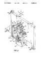
- FIG. 2illustrates the monolithic stage 40 coupled to the U-shaped bracket 36, and the reference surface 42.
- Reference surface 42is placed between the sub-stage 14 illustrated in FIG. 1 and the monolithic stage 40.
- a coil plate 44is rigidly attached to the U-shaped bracket 36.
- the monolithic body 46 of monolithic stage 40is coupled to the coil plate 44 by four electromagnetic coils 56 and 58.
- Two electromagnetic coil 56controls relative motion of the monolithic body 46 in the Y direction. Only one of the two coils 56 is illustrated in the cut-away portion in FIG. 2.
- Another coil 56is located adjacent the side opposite of the coil 56 illustrated.
- Two electromagnetic coils 58control the relative movement of the monolithic body 46 in the X direction. Only one coil 58 is illustrated in the cut-away portion in FIG. 2.
- the other coil 58is located adjacent the side opposite the coil 58 illustrated.
- Four electromagnetic focus coils 52are positioned at each corner of the monolithic body 46. Only one focus coil 52 is illustrated in the cut-away portion in FIG. 2. The focus coils 52 move the monolithic body 46 in the focus or Z direction. The focus coils 52 therefore control the distance of the monolithic body 46 from the reference surface 42. The weight of monolithic body 46 is compensated for by monolithic counter force means 50.
- Three air bearings 48only two being illustrated in FIG. 2, glide on the reference surface 42.
- Three cap gauges 54only two being illustrated in the perspective view in FIG. 2, are used to detect the position of the monolithic body 46 of the monolithic stage 40 on the Z axis.
- the air bearings 48are attached to the monolithic body 46 by three flexures 47. Associated with air bearings 48, and attached to the monolithic body 46 are three mechanical stops 49. Only two of the three mechanical stops 49 are illustrated in FIG. 2. The third mechanical stop is on the side hidden from view by the interferometer mirror 62 in FIG. 2. The mechanical stops 49 are adjustable and prevent the monolithic body 46 from moving out of a predetermined range of travel along the Z axis. This prevents unintentional contact with the surface 42 or projection optics, not illustrated.
- the structure of the monolithic stage and the controls and coupling to the sub-stageare similar to those disclosed in U.S. Pat. No. 4,952,858, which is herein incorporated by reference.
- Attached to the monolithic body 46is a wafer chuck 60.
- Laser gaugesare used in conjunction with interferometer mirrors 62 to accurately ascertain the position of the monolithic body 46 of the monolithic stage 40.
- Relative position sensor means 55is associated with the coil plate 44 attached to the sub-stage 14, illustrated in FIG. 1, and the monolithic body 46 to detect the relative position between the monolithic body 46 and coil plate 44, which is attached to the sub-stage 14 by U-shaped bracket 36. Damped, flexured, differential rods 64 are used to adjust and maintain the positioning of the reference surface 42.
- FIG. 3schematically represents the operation of the present invention.
- the reference surface 42is positioned between the sub-stage 14 and the monolithic stage 40.
- Focus or Z sensor 54is used to detect the distance between the reference surface 42 and the monolithic stage 40.
- Relative position sensor means 55is associated with the monolithic stage 40 and the sub-stage 14 through U-shaped bracket 36 in order to detect the relative position of the monolithic stage 40 and the sub-stage 14.
- Follow control means 66is coupled to the sub-stage 14, the relative position sensor means 55, and the monolithic stage 40.
- the follow control means 66provides a means for controlling the position of the sub-stage 14 to follow the approximate position of the monolithic stage 40.
- the monolithic stage 40is servo controlled, and the sub-stage 14 tracks the position of the monolithic stage 40 to keep the monolithic stage centered in a predetermined position.
- the predetermined positionis typically a position where the coils 56 and 58, illustrated in FIG. 2, are centered within their associated magnetic structures. Stop 49 and air bearing 48 limit travel of the monolithic stage 40 to a predetermined range preventing the possibility of striking the reference surface, projection optics, not shown, or any other nearby structure.
- the wafer stage of the present inventionprovides for improved focusing and positioning accuracy in addition to providing a greater range of travel.
- the greater range of travelimproves operation and permits easier cleaning and servicing of the monolithic stage. Additionally, the monolithic stage can be readily removed for inspection and repair.
Landscapes
- Engineering & Computer Science (AREA)
- Physics & Mathematics (AREA)
- General Physics & Mathematics (AREA)
- Condensed Matter Physics & Semiconductors (AREA)
- Manufacturing & Machinery (AREA)
- Computer Hardware Design (AREA)
- Microelectronics & Electronic Packaging (AREA)
- Power Engineering (AREA)
- Health & Medical Sciences (AREA)
- General Health & Medical Sciences (AREA)
- Orthopedic Medicine & Surgery (AREA)
- Robotics (AREA)
- Mechanical Engineering (AREA)
- Container, Conveyance, Adherence, Positioning, Of Wafer (AREA)
- Exposure Of Semiconductors, Excluding Electron Or Ion Beam Exposure (AREA)
- Exposure And Positioning Against Photoresist Photosensitive Materials (AREA)
- Machine Tool Units (AREA)
Abstract
Description
Claims (11)
Priority Applications (6)
| Application Number | Priority Date | Filing Date | Title |
|---|---|---|---|
| US08/015,520US5285142A (en) | 1993-02-09 | 1993-02-09 | Wafer stage with reference surface |
| JP10852393AJP3325077B2 (en) | 1993-02-09 | 1993-05-10 | Electromagnetic alignment device |
| DE69428617TDE69428617T2 (en) | 1993-02-09 | 1994-01-24 | Electromagnetic adjustment device |
| EP94300499AEP0611062B1 (en) | 1993-02-09 | 1994-01-24 | Electromagnetic alignment apparatus |
| CA002114059ACA2114059A1 (en) | 1993-02-09 | 1994-01-24 | Wafer stage with reference surface |
| KR1019940002322AKR100283784B1 (en) | 1993-02-09 | 1994-02-08 | Wafer stage with reference surface |
Applications Claiming Priority (1)
| Application Number | Priority Date | Filing Date | Title |
|---|---|---|---|
| US08/015,520US5285142A (en) | 1993-02-09 | 1993-02-09 | Wafer stage with reference surface |
Publications (1)
| Publication Number | Publication Date |
|---|---|
| US5285142Atrue US5285142A (en) | 1994-02-08 |
Family
ID=21771876
Family Applications (1)
| Application Number | Title | Priority Date | Filing Date |
|---|---|---|---|
| US08/015,520Expired - LifetimeUS5285142A (en) | 1993-02-09 | 1993-02-09 | Wafer stage with reference surface |
Country Status (6)
| Country | Link |
|---|---|
| US (1) | US5285142A (en) |
| EP (1) | EP0611062B1 (en) |
| JP (1) | JP3325077B2 (en) |
| KR (1) | KR100283784B1 (en) |
| CA (1) | CA2114059A1 (en) |
| DE (1) | DE69428617T2 (en) |
Cited By (29)
| Publication number | Priority date | Publication date | Assignee | Title |
|---|---|---|---|---|
| GB2290658A (en)* | 1994-06-27 | 1996-01-03 | Nikon Corp | Electromagnetic alignment and scanning apparatus |
| US5528118A (en)* | 1994-04-01 | 1996-06-18 | Nikon Precision, Inc. | Guideless stage with isolated reaction stage |
| US5574556A (en)* | 1993-06-30 | 1996-11-12 | Canon Kabushiki Kaisha | Stage mechanism in exposure apparatus |
| US5623853A (en)* | 1994-10-19 | 1997-04-29 | Nikon Precision Inc. | Precision motion stage with single guide beam and follower stage |
| WO1997021977A1 (en)* | 1995-12-11 | 1997-06-19 | Adagio Associates, Inc. | Integrated silicon profilometer and afm head |
| US5656942A (en)* | 1995-07-21 | 1997-08-12 | Electroglas, Inc. | Prober and tester with contact interface for integrated circuits-containing wafer held docked in a vertical plane |
| US5757160A (en)* | 1996-12-23 | 1998-05-26 | Svg Lithography Systems, Inc. | Moving interferometer wafer stage |
| US5760564A (en)* | 1995-06-27 | 1998-06-02 | Nikon Precision Inc. | Dual guide beam stage mechanism with yaw control |
| US5789830A (en)* | 1997-07-08 | 1998-08-04 | Systems, Machines, Automation Components Corporation | In-line rotational drive |
| US5861549A (en)* | 1996-12-10 | 1999-01-19 | Xros, Inc. | Integrated Silicon profilometer and AFM head |
| US5874820A (en)* | 1995-04-04 | 1999-02-23 | Nikon Corporation | Window frame-guided stage mechanism |
| US6008500A (en)* | 1995-04-04 | 1999-12-28 | Nikon Corporation | Exposure apparatus having dynamically isolated reaction frame |
| US6089525A (en)* | 1997-10-07 | 2000-07-18 | Ultratech Stepper, Inc. | Six axis active vibration isolation and payload reaction force compensation system |
| US6246204B1 (en) | 1994-06-27 | 2001-06-12 | Nikon Corporation | Electromagnetic alignment and scanning apparatus |
| US6307619B1 (en) | 2000-03-23 | 2001-10-23 | Silicon Valley Group, Inc. | Scanning framing blade apparatus |
| US6479991B1 (en) | 1998-04-01 | 2002-11-12 | Canon Kabushiki Kaisha | Stage mechanism, exposure apparatus and device manufacturing method in which a coil unit of a driving mechanism is moved substantially in synchronism with a stage |
| US6538720B2 (en) | 2001-02-28 | 2003-03-25 | Silicon Valley Group, Inc. | Lithographic tool with dual isolation system and method for configuring the same |
| US20030090678A1 (en)* | 2001-11-15 | 2003-05-15 | Evans Christopher James | Rapid in situ mastering of an aspheric fizeau with residual error compensation |
| US20030128368A1 (en)* | 2001-11-15 | 2003-07-10 | Michael Kuchel | Dispersive null-optics for aspheric surface and wavefront metrology |
| US20030174304A1 (en)* | 2002-03-12 | 2003-09-18 | Asml Us Inc. | Method, system, and apparatus for management of reaction loads in a lithography system |
| US20030223125A1 (en)* | 2002-05-29 | 2003-12-04 | Asml Us, Inc. | Catadioptric lithography system and method with reticle stage orthogonal to wafer stage |
| US20050002009A1 (en)* | 1994-04-01 | 2005-01-06 | Nikon Corporation | Positioning device having dynamically isolated frame, and lithographic device provided with such a positioning device |
| US20050169784A1 (en)* | 2004-02-02 | 2005-08-04 | Poon Alex K.T. | Force provider for a mover assembly of a stage assembly |
| US20050236915A1 (en)* | 2004-04-23 | 2005-10-27 | Nikon Corporation | Electromagnetic force actuator |
| US20070131879A1 (en)* | 2004-02-02 | 2007-06-14 | Nikon Corporation | Force provider with adjustable force characteristics for a stage assembly |
| US7365513B1 (en) | 1994-04-01 | 2008-04-29 | Nikon Corporation | Positioning device having dynamically isolated frame, and lithographic device provided with such a positioning device |
| USRE40774E1 (en) | 1995-05-30 | 2009-06-23 | Asml Netherlands B.V. | Positioning device with a vibration-free object table, and lithographic device provided with such a positioning device |
| US7678458B2 (en) | 2007-01-24 | 2010-03-16 | Asml Holding N.V. | Bonding silicon silicon carbide to glass ceramics |
| CN102809346A (en)* | 2011-05-31 | 2012-12-05 | 上海微电子装备有限公司 | Position measuring device of motion platform and measuring method of position measuring device |
Families Citing this family (3)
| Publication number | Priority date | Publication date | Assignee | Title |
|---|---|---|---|---|
| KR100437263B1 (en)* | 2002-08-02 | 2004-06-23 | 한국과학기술원 | Long range stage of 6 degrees freedom using double h-frame |
| KR100568207B1 (en) | 2004-02-13 | 2006-04-05 | 삼성전자주식회사 | Conveyer |
| CN110000573A (en)* | 2019-05-08 | 2019-07-12 | 盐城盐东速削科技有限公司 | A kind of movable beam type speed based on magnetic levitation technology cuts machine |
Citations (6)
| Publication number | Priority date | Publication date | Assignee | Title |
|---|---|---|---|---|
| US4223257A (en)* | 1978-11-15 | 1980-09-16 | Miller Donald K | Adaptive servo control system |
| US4654571A (en)* | 1985-09-16 | 1987-03-31 | Hinds Walter E | Single plane orthogonally movable drive system |
| US4676649A (en)* | 1985-11-27 | 1987-06-30 | Compact Spindle Bearing Corp. | Multi-axis gas bearing stage assembly |
| US4742286A (en)* | 1985-10-29 | 1988-05-03 | Micro-Stage, Inc. | Gas bearing X-Y-θ stage assembly |
| US4952858A (en)* | 1988-05-18 | 1990-08-28 | Galburt Daniel N | Microlithographic apparatus |
| US5040431A (en)* | 1988-01-22 | 1991-08-20 | Canon Kabushiki Kaisha | Movement guiding mechanism |
Family Cites Families (1)
| Publication number | Priority date | Publication date | Assignee | Title |
|---|---|---|---|---|
| US5168512A (en)* | 1990-03-13 | 1992-12-01 | Canon Kabushiki Kaisha | Method of manufacture of semiconductor devices |
- 1993
- 1993-02-09USUS08/015,520patent/US5285142A/ennot_activeExpired - Lifetime
- 1993-05-10JPJP10852393Apatent/JP3325077B2/ennot_activeExpired - Fee Related
- 1994
- 1994-01-24EPEP94300499Apatent/EP0611062B1/ennot_activeExpired - Lifetime
- 1994-01-24DEDE69428617Tpatent/DE69428617T2/ennot_activeExpired - Fee Related
- 1994-01-24CACA002114059Apatent/CA2114059A1/ennot_activeAbandoned
- 1994-02-08KRKR1019940002322Apatent/KR100283784B1/ennot_activeExpired - Fee Related
Patent Citations (6)
| Publication number | Priority date | Publication date | Assignee | Title |
|---|---|---|---|---|
| US4223257A (en)* | 1978-11-15 | 1980-09-16 | Miller Donald K | Adaptive servo control system |
| US4654571A (en)* | 1985-09-16 | 1987-03-31 | Hinds Walter E | Single plane orthogonally movable drive system |
| US4742286A (en)* | 1985-10-29 | 1988-05-03 | Micro-Stage, Inc. | Gas bearing X-Y-θ stage assembly |
| US4676649A (en)* | 1985-11-27 | 1987-06-30 | Compact Spindle Bearing Corp. | Multi-axis gas bearing stage assembly |
| US5040431A (en)* | 1988-01-22 | 1991-08-20 | Canon Kabushiki Kaisha | Movement guiding mechanism |
| US4952858A (en)* | 1988-05-18 | 1990-08-28 | Galburt Daniel N | Microlithographic apparatus |
Cited By (92)
| Publication number | Priority date | Publication date | Assignee | Title |
|---|---|---|---|---|
| US5574556A (en)* | 1993-06-30 | 1996-11-12 | Canon Kabushiki Kaisha | Stage mechanism in exposure apparatus |
| US5744924A (en)* | 1994-04-01 | 1998-04-28 | Nikon Corporation | Guideless stage with isolated reaction frame |
| US5528118A (en)* | 1994-04-01 | 1996-06-18 | Nikon Precision, Inc. | Guideless stage with isolated reaction stage |
| US6271640B1 (en) | 1994-04-01 | 2001-08-07 | Nikon Corporation | Exposure apparatus having reaction frame |
| US7365513B1 (en) | 1994-04-01 | 2008-04-29 | Nikon Corporation | Positioning device having dynamically isolated frame, and lithographic device provided with such a positioning device |
| US20050002009A1 (en)* | 1994-04-01 | 2005-01-06 | Nikon Corporation | Positioning device having dynamically isolated frame, and lithographic device provided with such a positioning device |
| US6927840B2 (en) | 1994-04-01 | 2005-08-09 | Nikon Corporation | Positioning device having dynamically isolated frame, and lithographic device provided with such a positioning device |
| US6989647B1 (en) | 1994-04-01 | 2006-01-24 | Nikon Corporation | Positioning device having dynamically isolated frame, and lithographic device provided with such a positioning device |
| US6841965B2 (en) | 1994-04-01 | 2005-01-11 | Nikon Corporation | Guideless stage with isolated reaction stage |
| US6049186A (en)* | 1994-04-01 | 2000-04-11 | Nikon Corporation | Method for making and operating an exposure apparatus having a reaction frame |
| US5982128A (en)* | 1994-04-01 | 1999-11-09 | Nikon Corporation | Lithography apparatus with movable stage and mechanical isolation of stage drive |
| US5942871A (en)* | 1994-04-01 | 1999-08-24 | Nikon Corporation | Double flexure support for stage drive coil |
| US6281654B1 (en) | 1994-04-01 | 2001-08-28 | Nikon Corporation | Method for making apparatus with dynamic support structure isolation and exposure method |
| GB2329067B (en)* | 1994-06-27 | 1999-06-02 | Nikon Corp | Electromagnetioc alignment and scanning apparatus |
| US6969966B2 (en) | 1994-06-27 | 2005-11-29 | Nikon Corporation | Electromagnetic alignment and scanning apparatus |
| GB2329067A (en)* | 1994-06-27 | 1999-03-10 | Nikon Corp | Electromagnetic alignment and scanning apparatus |
| GB2290658B (en)* | 1994-06-27 | 1999-03-24 | Nikon Corp | Electromagnetic alignment and scanning apparatus |
| GB2325564B (en)* | 1994-06-27 | 1999-03-24 | Nikon Corp | Electromagnetic alignment and scanning apparatus |
| GB2325565B (en)* | 1994-06-27 | 1999-03-31 | Nikon Corp | Electromagnetic alignment and scanning apparatus |
| GB2325566B (en)* | 1994-06-27 | 1999-03-31 | Nikon Corp | Electromagnetic alignment and scanning apparatus |
| GB2325565A (en)* | 1994-06-27 | 1998-11-25 | Nikon Corp | Electromagnetic alignment and scanning apparatus |
| GB2325566A (en)* | 1994-06-27 | 1998-11-25 | Nikon Corp | Electromagnetic scanning and alignment apparatus |
| GB2325564A (en)* | 1994-06-27 | 1998-11-25 | Nikon Corp | Electromagnetic alignment and scanning apparatus |
| GB2290658A (en)* | 1994-06-27 | 1996-01-03 | Nikon Corp | Electromagnetic alignment and scanning apparatus |
| US20050083006A1 (en)* | 1994-06-27 | 2005-04-21 | Nikon Corporation | Electromagnetic alignment and scanning apparatus |
| US6844696B2 (en) | 1994-06-27 | 2005-01-18 | Nikon Corporation | Electromagnetic alignment and scanning apparatus |
| US20050088133A1 (en)* | 1994-06-27 | 2005-04-28 | Nikon Corporation | Electromagnetic alignment and scanning apparatus |
| US6844695B2 (en) | 1994-06-27 | 2005-01-18 | Nikon Corporation | Electromagnetic alignment and scanning apparatus |
| US20050280390A1 (en)* | 1994-06-27 | 2005-12-22 | Nikon Corporation | Electromagnetic alignment and scanning apparatus |
| US7012398B2 (en) | 1994-06-27 | 2006-03-14 | Nikon Corporation | Electromagnetic alignment and scanning apparatus |
| US6693402B2 (en) | 1994-06-27 | 2004-02-17 | Nikon Corporation | Electromagnetic alignment and scanning apparatus |
| US20030184254A1 (en)* | 1994-06-27 | 2003-10-02 | Nikon Corporation | Electromagnetic alignment and scanning apparatus |
| US20030184253A1 (en)* | 1994-06-27 | 2003-10-02 | Nikon Corporation | Electromagnetic alignment and scanning apparatus |
| US6246204B1 (en) | 1994-06-27 | 2001-06-12 | Nikon Corporation | Electromagnetic alignment and scanning apparatus |
| US6329780B1 (en) | 1994-06-27 | 2001-12-11 | Nikon Corporation | Electromagnetic alignment and scanning apparatus |
| US6252370B1 (en) | 1994-06-27 | 2001-06-26 | Nikon Corporation | Electromagnetic alignment and scanning apparatus |
| US6255796B1 (en) | 1994-06-27 | 2001-07-03 | Nikon Corporation | Electromagnetic alignment and scanning apparatus |
| US6255795B1 (en) | 1994-06-27 | 2001-07-03 | Nikon Corporation | Electromagnetic alignment and scanning apparatus |
| US7573225B2 (en) | 1994-06-27 | 2009-08-11 | Nikon Corporation | Electromagnetic alignment and scanning apparatus |
| US6323935B1 (en) | 1994-06-27 | 2001-11-27 | Nikon Corporation | Electromagnetic alignment and scanning apparatus |
| US5996437A (en)* | 1994-10-19 | 1999-12-07 | Nikon Corporation | Precision motion stage with single guide beam and follower stage |
| US5623853A (en)* | 1994-10-19 | 1997-04-29 | Nikon Precision Inc. | Precision motion stage with single guide beam and follower stage |
| US6087797A (en)* | 1995-04-04 | 2000-07-11 | Nikon Corporation | Exposure method, and method of making exposure apparatus having dynamically isolated reaction frame |
| US6150787A (en)* | 1995-04-04 | 2000-11-21 | Nikon Corporation | Exposure apparatus having dynamically isolated reaction frame |
| US6246202B1 (en) | 1995-04-04 | 2001-06-12 | Nikon Corporation | Method of making exposure apparatus with dynamically isolated reaction frame |
| US6316901B2 (en) | 1995-04-04 | 2001-11-13 | Nikon Corporation | Exposure apparatus and method utilizing isolated reaction frame |
| US20040095085A1 (en)* | 1995-04-04 | 2004-05-20 | Nikon Corporation | Window frame-guided stage mechanism |
| US6020710A (en)* | 1995-04-04 | 2000-02-01 | Nikon Corporation | Exposure method, and method of making exposure apparatus having dynamically isolated reaction frame |
| US6747732B1 (en) | 1995-04-04 | 2004-06-08 | Nikon Corporation | Method of making exposure apparatus with dynamically isolated reaction frame |
| US6151105A (en)* | 1995-04-04 | 2000-11-21 | Nikon Corporation | Exposure apparatus having dynamically isolated support structure |
| US5874820A (en)* | 1995-04-04 | 1999-02-23 | Nikon Corporation | Window frame-guided stage mechanism |
| US6188195B1 (en) | 1995-04-04 | 2001-02-13 | Nikon Corporation | Exposure method, and method of making exposure apparatus having dynamically isolated support structure |
| US6175404B1 (en) | 1995-04-04 | 2001-01-16 | Nikon Corporation | Exposure apparatus having dynamically isolated reaction frame |
| US6008500A (en)* | 1995-04-04 | 1999-12-28 | Nikon Corporation | Exposure apparatus having dynamically isolated reaction frame |
| US6683433B2 (en) | 1995-04-04 | 2004-01-27 | Nikon Corporation | Exposure apparatus and method utilizing isolated reaction frame |
| USRE40774E1 (en) | 1995-05-30 | 2009-06-23 | Asml Netherlands B.V. | Positioning device with a vibration-free object table, and lithographic device provided with such a positioning device |
| US5760564A (en)* | 1995-06-27 | 1998-06-02 | Nikon Precision Inc. | Dual guide beam stage mechanism with yaw control |
| US5656942A (en)* | 1995-07-21 | 1997-08-12 | Electroglas, Inc. | Prober and tester with contact interface for integrated circuits-containing wafer held docked in a vertical plane |
| WO1997021977A1 (en)* | 1995-12-11 | 1997-06-19 | Adagio Associates, Inc. | Integrated silicon profilometer and afm head |
| US6272907B1 (en) | 1995-12-11 | 2001-08-14 | Xros, Inc. | Integrated silicon profilometer and AFM head |
| US5861549A (en)* | 1996-12-10 | 1999-01-19 | Xros, Inc. | Integrated Silicon profilometer and AFM head |
| US5757160A (en)* | 1996-12-23 | 1998-05-26 | Svg Lithography Systems, Inc. | Moving interferometer wafer stage |
| US5789830A (en)* | 1997-07-08 | 1998-08-04 | Systems, Machines, Automation Components Corporation | In-line rotational drive |
| US6089525A (en)* | 1997-10-07 | 2000-07-18 | Ultratech Stepper, Inc. | Six axis active vibration isolation and payload reaction force compensation system |
| US6479991B1 (en) | 1998-04-01 | 2002-11-12 | Canon Kabushiki Kaisha | Stage mechanism, exposure apparatus and device manufacturing method in which a coil unit of a driving mechanism is moved substantially in synchronism with a stage |
| US6307619B1 (en) | 2000-03-23 | 2001-10-23 | Silicon Valley Group, Inc. | Scanning framing blade apparatus |
| US20030164931A1 (en)* | 2001-02-28 | 2003-09-04 | Silicon Valley Group, Inc. | Lithographic tool with dual isolation system and method for configuring the same |
| US6538720B2 (en) | 2001-02-28 | 2003-03-25 | Silicon Valley Group, Inc. | Lithographic tool with dual isolation system and method for configuring the same |
| US7164463B2 (en) | 2001-02-28 | 2007-01-16 | Asml Holding N.V. | Lithographic tool with dual isolation system and method for configuring the same |
| US7158213B2 (en) | 2001-02-28 | 2007-01-02 | Asml Holding N.V. | Lithographic tool with dual isolation system and method for configuring the same |
| US6734979B2 (en) | 2001-11-15 | 2004-05-11 | Zygo Corporation | Rapid in situ mastering of an aspheric Fizeau with residual error compensation |
| US20030090678A1 (en)* | 2001-11-15 | 2003-05-15 | Evans Christopher James | Rapid in situ mastering of an aspheric fizeau with residual error compensation |
| US6717679B2 (en) | 2001-11-15 | 2004-04-06 | Zygo Corporation | Dispersive null-optics for aspheric surface and wavefront metrology |
| US20030128368A1 (en)* | 2001-11-15 | 2003-07-10 | Michael Kuchel | Dispersive null-optics for aspheric surface and wavefront metrology |
| US20040207830A1 (en)* | 2002-03-12 | 2004-10-21 | Asml Holding, N.V. | Method, system, and apparatus for management of reaction loads in a lithography system |
| US6885435B2 (en) | 2002-03-12 | 2005-04-26 | Asml Holding N.V. | Method, system, and apparatus for management of reaction loads in a lithography system |
| US6784978B2 (en) | 2002-03-12 | 2004-08-31 | Asml Holding N.V. | Method, system, and apparatus for management of reaction loads in a lithography system |
| US6989889B2 (en) | 2002-03-12 | 2006-01-24 | Asml Holding N.V. | Method, system, and apparatus for management of reaction loads in a lithography system |
| US20050185163A1 (en)* | 2002-03-12 | 2005-08-25 | Galburt Daniel N. | Method, system, and apparatus for management of reaction loads in a lithography system |
| US20030174304A1 (en)* | 2002-03-12 | 2003-09-18 | Asml Us Inc. | Method, system, and apparatus for management of reaction loads in a lithography system |
| US6977716B2 (en) | 2002-05-29 | 2005-12-20 | Asml Holding N.V. | Catadioptric lithography system and method with reticle stage orthogonal to wafer stage |
| US6757110B2 (en) | 2002-05-29 | 2004-06-29 | Asml Holding N.V. | Catadioptric lithography system and method with reticle stage orthogonal to wafer stage |
| US20030223125A1 (en)* | 2002-05-29 | 2003-12-04 | Asml Us, Inc. | Catadioptric lithography system and method with reticle stage orthogonal to wafer stage |
| US20040201830A1 (en)* | 2002-05-29 | 2004-10-14 | Harry Sewell | Catadioptric lithography system and method with reticle stage orthogonal to wafer stage |
| US20070131879A1 (en)* | 2004-02-02 | 2007-06-14 | Nikon Corporation | Force provider with adjustable force characteristics for a stage assembly |
| US20050169784A1 (en)* | 2004-02-02 | 2005-08-04 | Poon Alex K.T. | Force provider for a mover assembly of a stage assembly |
| US20050236915A1 (en)* | 2004-04-23 | 2005-10-27 | Nikon Corporation | Electromagnetic force actuator |
| US7678458B2 (en) | 2007-01-24 | 2010-03-16 | Asml Holding N.V. | Bonding silicon silicon carbide to glass ceramics |
| US20100128242A1 (en)* | 2007-01-24 | 2010-05-27 | Asml Holding N.V. | Bonding Silicon Silicon Carbide to Glass Ceramics |
| US8168017B2 (en) | 2007-01-24 | 2012-05-01 | Asml Holding N.V. | Bonding silicon silicon carbide to glass ceramics |
| CN102809346A (en)* | 2011-05-31 | 2012-12-05 | 上海微电子装备有限公司 | Position measuring device of motion platform and measuring method of position measuring device |
| CN102809346B (en)* | 2011-05-31 | 2014-12-17 | 上海微电子装备有限公司 | Position measuring device of motion platform and measuring method of position measuring device |
Also Published As
| Publication number | Publication date |
|---|---|
| JPH06252034A (en) | 1994-09-09 |
| CA2114059A1 (en) | 1994-08-10 |
| EP0611062B1 (en) | 2001-10-17 |
| DE69428617D1 (en) | 2001-11-22 |
| JP3325077B2 (en) | 2002-09-17 |
| EP0611062A1 (en) | 1994-08-17 |
| DE69428617T2 (en) | 2002-08-01 |
| KR940020524A (en) | 1994-09-16 |
| KR100283784B1 (en) | 2001-04-02 |
Similar Documents
| Publication | Publication Date | Title |
|---|---|---|
| US5285142A (en) | Wafer stage with reference surface | |
| US6841965B2 (en) | Guideless stage with isolated reaction stage | |
| KR100314554B1 (en) | An exposure apparatus and an exposure method | |
| CA1304173C (en) | Microlithographic apparatus | |
| EP0327949B1 (en) | Alignment stage device | |
| US6989647B1 (en) | Positioning device having dynamically isolated frame, and lithographic device provided with such a positioning device | |
| US20050280390A1 (en) | Electromagnetic alignment and scanning apparatus | |
| GB2325565A (en) | Electromagnetic alignment and scanning apparatus | |
| US5066131A (en) | Stage mechanism | |
| US7365513B1 (en) | Positioning device having dynamically isolated frame, and lithographic device provided with such a positioning device | |
| KR20010043861A (en) | Exposure method and exposure apparatus | |
| US20060061751A1 (en) | Stage assembly including a stage having increased vertical stroke | |
| JPH04317Y2 (en) | ||
| JP2000182931A (en) | Exposure equipment | |
| JP4287781B2 (en) | Positioning device having a reference frame for a measurement system | |
| KR100434618B1 (en) | Positioning device with reference frame for measuring system | |
| JP2711898B2 (en) | Non-contact guide type positioning table | |
| KR100430494B1 (en) | Positioning apparatus having an object table without the influence of vibration and lithographic apparatus provided with the positioning apparatus | |
| WO1998049709A1 (en) | Pattern-writing machine |
Legal Events
| Date | Code | Title | Description |
|---|---|---|---|
| AS | Assignment | Owner name:SVGT LITHOGRAPHY SYSTEMS, INC., CONNECTICUT Free format text:ASSIGNMENT OF ASSIGNORS INTEREST.;ASSIGNORS:GALBURT, DANIEL N.;O'CONNER, GEOFFREY;REEL/FRAME:006432/0623 Effective date:19930128 | |
| STCF | Information on status: patent grant | Free format text:PATENTED CASE | |
| FPAY | Fee payment | Year of fee payment:4 | |
| FPAY | Fee payment | Year of fee payment:8 | |
| FEPP | Fee payment procedure | Free format text:PAYOR NUMBER ASSIGNED (ORIGINAL EVENT CODE: ASPN); ENTITY STATUS OF PATENT OWNER: LARGE ENTITY | |
| AS | Assignment | Owner name:ASML HOLDING N.V., NETHERLANDS Free format text:CERTIFICATE OF OWNERSHIP AND MERGER, CONVERSION, MERGER, AND CONFIRMATORY ASSIGNMENT;ASSIGNORS:SVG LITHOGRAPHY SYSTEMS, INC.;ASML US, INC.;ASM LITHOGRAPHY, INC. AND ASML US, LLC;AND OTHERS;REEL/FRAME:014484/0588;SIGNING DATES FROM 20011231 TO 20031009 Owner name:ASML US, INC., ARIZONA Free format text:CERTIFICATE OF OWNERSHIP AND MERGER, CONVERSION, MERGER, AND CONFIRMATORY ASSIGNMENT;ASSIGNORS:SVG LITHOGRAPHY SYSTEMS, INC.;ASML US, INC.;ASM LITHOGRAPHY, INC. AND ASML US, LLC;AND OTHERS;REEL/FRAME:014484/0588;SIGNING DATES FROM 20011231 TO 20031009 Owner name:ASML US, LLC, DELAWARE Free format text:CERTIFICATE OF OWNERSHIP AND MERGER, CONVERSION, MERGER, AND CONFIRMATORY ASSIGNMENT;ASSIGNORS:SVG LITHOGRAPHY SYSTEMS, INC.;ASML US, INC.;ASM LITHOGRAPHY, INC. AND ASML US, LLC;AND OTHERS;REEL/FRAME:014484/0588;SIGNING DATES FROM 20011231 TO 20031009 | |
| FPAY | Fee payment | Year of fee payment:12 |