US5283761A - Method of multi-level storage in DRAM - Google Patents
Method of multi-level storage in DRAMDownload PDFInfo
- Publication number
- US5283761A US5283761AUS07/916,673US91667392AUS5283761AUS 5283761 AUS5283761 AUS 5283761AUS 91667392 AUS91667392 AUS 91667392AUS 5283761 AUS5283761 AUS 5283761A
- Authority
- US
- United States
- Prior art keywords
- voltage
- sub
- bitline
- cell
- level
- Prior art date
- Legal status (The legal status is an assumption and is not a legal conclusion. Google has not performed a legal analysis and makes no representation as to the accuracy of the status listed.)
- Ceased
Links
Images


Classifications
- G—PHYSICS
- G11—INFORMATION STORAGE
- G11C—STATIC STORES
- G11C11/00—Digital stores characterised by the use of particular electric or magnetic storage elements; Storage elements therefor
- G11C11/56—Digital stores characterised by the use of particular electric or magnetic storage elements; Storage elements therefor using storage elements with more than two stable states represented by steps, e.g. of voltage, current, phase, frequency
- G11C11/565—Digital stores characterised by the use of particular electric or magnetic storage elements; Storage elements therefor using storage elements with more than two stable states represented by steps, e.g. of voltage, current, phase, frequency using capacitive charge storage elements
- G—PHYSICS
- G11—INFORMATION STORAGE
- G11C—STATIC STORES
- G11C2211/00—Indexing scheme relating to digital stores characterized by the use of particular electric or magnetic storage elements; Storage elements therefor
- G11C2211/56—Indexing scheme relating to G11C11/56 and sub-groups for features not covered by these groups
- G11C2211/563—Multilevel memory reading aspects
- G11C2211/5634—Reference cells
- G—PHYSICS
- G11—INFORMATION STORAGE
- G11C—STATIC STORES
- G11C7/00—Arrangements for writing information into, or reading information out from, a digital store
- G11C7/06—Sense amplifiers; Associated circuits, e.g. timing or triggering circuits
Definitions
- This inventionrelates to dynamic random access memory (DRAM) memories, and in particular to a method of storing a variable level signal in each cell of a DRAM for representing more than one bit in each cell.
- DRAMdynamic random access memory
- a second problem with multi-bit storage cellsrelates to the method of sensing.
- No simple method of sensinghas previously been designed, although attempts have been made to solve this problem, e.g. as described in the publication by M. Aoki et al, "A 16-Levels/Cell Dynamic Memory", ISSCC Dig. TECH. Papers 1985, pp 246-247, and in T. Furuyama et al, "An Experimental Two-Bit/Cell Storage DRAM for Macrocell or Memory-On-Application", IEEE Journal of Solid State Circuits, Vol. 24, No. 2, pp 388-393, April 1989.
- the technique described by Aokicannot use normal sense amplifiers.
- DRAMshave previously been built with cells holding up to sixteen bits of storage, e.g. in the aforenoted article by M. Aoki et al, for use in file memories.
- a 4 K test arrayis believed to have been the largest memory built using this design. Leakage characteristics of the DRAM cell were required to be very tightly controlled and even then, accurate sensing of the small voltage differences between levels becomes very difficult.
- Another problem with this schemewas the length of time required to access: a single read cycle required 16 clocks for the read followed by 16 clocks for the restore.
- the cellcan define the cell as storing one of four voltage levels V cell0 , V cell1 , V cell2 and V cell3 , and reference voltage midpoints between these four voltage, which can be defined as V ref1 , V ref2 and V ref3 . These midpoints can be referred to, to differentiate between the four voltage levels. The relative voltage of these levels are shown in Table 1 below.
- the storage voltagesare the actual voltages stored in the cells, although the sensing voltages are somewhat more attenuated. Since sensing takes place on the bitlines which divide cell charge by the cell to bitline capacitance ratio, much lower voltages than those in the cell are actually sensed. In a standard DRAM, these voltage differences are in the order of 100-300 mV. It is the voltage midpoints between these smaller signals that must finally be generated to allow for correct sensing.
- Furuyama et al in the article noted abovedescribes one method of sensing these voltages.
- Furuyama et alused three sense amplifiers and three approximate midpoint sensing voltages.
- the cell chargeis shared with the bitline, the bitline is split into three sections (sub-bitlines) and three sense amplifiers determine whether the cell charge is above or below their particular reference voltages.
- This datais then converted to two bits and a resulting output. Reconversion of the two bits allows approximate values to be driven into the bitline so that restore takes place after the read cycle.
- a write cycleoperates in the same way as the restore section of the read cycle.
- the reference voltageis about three times larger than it should be for sensing, casting doubt on the operability of this design.
- three sense amplifiersare used, and since sense amplifiers have been growing proportionally larger and larger with each generation of memory, a minimum of sense amplifiers is desirable.
- a third problemis that the reference voltage is stored on a cell whose leakage does not track the leakage of the data cells, introducing another source of error into the circuit.
- a method and circuithas been designed which substantially solves the above-identified problems. Only two sense amplifiers are required, which generate the sensing voltages at the time of sensing. In the present invention each bitline is split exactly in half, rather than into thirds, by use of a switch.
- the noise marginsare relatively large, equivalent to that of a standard DRAM maintaining reliability, and the present design can be used as a standard one bit per cell DRAM as an alternative to a multiple bit per cell DRAM, which increases its universality, allows it to be used in present designs, and increases yield.
- a method of processing data having one of four levels stored in a DRAM cellis comprised of sensing whether or not the data voltage is above or below a voltage level midway between a highest and a lowest of the four levels, setting the voltage on a reference line higher than the lowest and lower than the next highest of the four levels in the event the data voltage is below the midway voltage level, setting the voltage on the reference line higher than the second highest and lower than the highest of the four levels in the event the data voltage is above the midway point, and sensing whether the data voltage is higher or lower in voltage than the reference line, whereby which of the four levels the data bit occupies is read.
- a method of processing data having one of plural levels stored in a DRAM cell capacitoris comprised of dumping the charge of the cell capacitor on a first of a pair of conductors of a folded bitline, maintaining the other of the pair of conductors split into other sub-bitline conductors and charging each of the other sub-bitline conductors to an intermediate voltage, splitting the first of the conductors into first sub-bitline conductors, sensing the sub-bitlines to determine whether the charge of the cell has a higher voltage than the intermediate voltage of one of the other sub-bitline conductors and providing a logic level result signal, storing the logic level result signal in a dummy cell capacitor, setting a charge storage capacitor and all of the sub-bitlines other than the first sub-bitline maintaining a voltage resulting from the dumped charge to a predetermined voltage, dumping charge stored in the dummy cell capacitor on the sub-bitlines and charge storage capacitor, thereby varying the predetermined voltage stored thereon to a degree
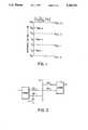
- FIG. 1is a diagram illustrating various voltage levels referred to in the description
- FIG. 2is a block diagram used to illustrate the basic concepts of the invention
- FIG. 3illustrates a block diagram in six steps of a read cycle
- FIG. 4illustrates in block diagram two steps of a write or restore cycle
- FIG. 5is a schematic diagram illustrating an embodiment of the invention.
- FIG. 6illustrates a timing diagram of the schematic illustrated in FIG. 5.
- the cell capacitorFor a DRAM cell to store two bits using a single cell capacitor, the cell capacitor should store one of four voltage values V cell0 , V cell1 , V cell2 or V cell3 , wherein V cell0 represents the lowest and V cell3 represents the highest cell voltage. To differentiate between the voltages, mid-point voltages V ref1 , V ref2 and V ref3 are defined, as shown in FIG. 1.
- V ref1is one-sixth the highest voltage V DD
- V cell1is one-third V DD
- V ref2is one-half V DD
- V cell2is two-thirds V DD
- V ref3is five-sixths V DD and V cell3 equals V DD .
- V ref1is midway between V cell0 and V cell1
- V ref2is midway between V cell0 and V cell3
- V ref3is midway between V cell2 and V cell3 .
- FIG. 2will be used to illustrate the basic concept of the invention.
- a sense amplifier 1can be connected to a pair of conductors 3A and 3B which form a folded bitline.
- Another sense amplifier 5can be connected to a pair of conductors 7A and 7B which form the remainder of the folded bitline.
- conductor 7Ais a continuation of conductor 3A
- conductor 7Bis a continuation of conductor 3B.
- the bitlineis shown split in half as shown by dotted line 9.
- any of the sub-bitline conductorsmay be connected to any others, e.g. via FET switches.
- Capacitor 11represents a cell on which charge is stored in one of four voltage levels. It is desired to read the level and output two binary bits representing the charge level stored on capacitor 11.
- sub-bitline conductor 7Acan be brought to V ref2 , which is one-half V DD .
- the voltage on sub-bitline 3B resulting from the charge stored on cell capacitor 11is then compared with the voltage on conductor 7A to determine whether it is above or below V ref2 .
- the continuous conductor 3A-7Bis brought to V ref3 , which is midway between the voltage level V cell2 and V cell3 . If the voltage on conductor 3B is below V ref2 , then the voltage on continuous conductor 3A, 7B is brought to V ref1 , which is midway between the V cell1 and V cell0 voltages.
- the continuous conductor 3A, 7Bis referred to herein as a reference line.
- the voltage on the reference lineis either above or below one-half V DD , i.e. V ref2 , and is established midway between the only two voltages Which conductor 3B can have, V cell0 and V cell1 , or V cell2 and V cell3 .
- the voltage on sub-bitline 3Bis then compared with the voltage on the reference line to determine whether it is above or below that voltage. If it is above that voltage the logic voltage must be either V cell1 or V cell3 ; whichever one it is, was established by the first determination of whether the voltage on conductor 3B was above or below the midway voltage V ref2 . Similarly if the voltage on conductor 3B is below the voltage on the reference line, the logic output represents either V cell0 or V cell2 , and again whichever one it is, was previously determined by the original determination of whether the voltage on conductor 3B is below or above V ref2 . In practice, the voltage on conductor 3B could be compared again With V ref2 , which is on lead 7A, to select which of either of the two cell voltage possibilities should be selected.
- FIG. 3illustrates in more detail a sequence of the steps in the process.
- first bitlines BL and BL*These bitline references are not shown as such, but their connection points to a pair of sense amplifiers 13 and 15 are shown referenced BL and BL*.
- Sense amplifier 13is provided to sense bit 0 and sense amplifier 15 is provided to sense bit 1. It is important that bitlines should be able to be split exactly in half, e.g. by apparatus such as a switch into sub-bitline conductors BLA, BLB, BL*A and BL*B.
- the sense amplifierscan be enabled or disabled as required.
- Prior to step 1all bitline segments are charged to the voltage V ref2 which is 1/2 V bb .
- step 1sub-bitlines BL A and BL B are disconnected from the V ref2 reference voltage, connected together and the sense amplifiers are not connected to the bitline.
- the cell capacitor 11then dumps its charge onto the BL line formed of conductors BL A and BL B , resulting in a voltage which for example is ##EQU1## where C S is the cell capacitance and C BL is the capacitance of the entire bitline.
- V ref2which is 1/2 V DD is applied to the BL* conductors BL* A and BL* B .
- step 2the two halves of the BL conductor are separated, and the bit 1 sense amplifier is connected to sense the voltage on conductor BL B to determine whether it is above or below the voltage V ref2 which is on the BL *B conductor. Since the voltage is V cell2 which is above V ref2 , a logic level one signal is stored in dummy cell 17 which is connected to the BL B lead.
- step 3the sense amplifier 15 and dummy cell 17 are disconnected from the bitline, and charge storage Ccell capacitor 18 is connected to lead BL B .
- Conductors BL B , BL* B , and BL* Aare all connected together, and the midpoint voltage V ref2 is applied thereto.
- step 4the logic level signal stored in dummy cell 17 is dumped to the sub-bitlines BL B , BL* B and BL* A .
- the chargeis also shared with Ccell 18, which has one half the capacitance of a normal cell. This charge sharing on the three half bitlines plus Ccell creates the exact reference level needed for the 2nd phase of sensing.
- the total capacity of the Ccell 18should be established so that the resulting voltage on the sub-bitlines is, in this example, V ref3 .
- V ref3the voltage on the Ccell and sub-bitlines was established at V ref2 , one-half V DD in step 3, with the charge on dummy cell 17 having been established with full logic level V DD in step 2, when it is connected to the combined sub-bitlines in step 4, its charge, being shared with the Ccell, should result in a voltage ##EQU2## i.e. V ref3 , which is midway between V cell2 and V cell3 .
- step 2If in step 2 the sensed bit was a zero, charge on dummy cell 17 would have been zero or V ss . When connected to the combined bitlines in step 4 it would receive charge from the Ccell 18, causing a reduction in voltage to V ref1 , which is midway between V cell1 and V cell0 .
- the combined sub-bitlinesform a reference line, the voltage of which can be compared with that on cell 11, and corresponds to reference line 3A, 7B described with reference to FIG. 2.
- step 5the Ccells 18 and dummy cell 17 are disconnected and each of the sub-bitlines are isolated.
- the voltage V ref2 of one-half V DDis applied to the sub-bitline BL* B . It may be seen that the sub-bitline BL* B is now at the midpoint V ref2 , both sub-bitlines BL* A and BL B are at the reference line voltage V ref3 (or V ref1 if the original cell voltage had been below V ref2 ), and the sub-bitline BLA is at the cell capacitor 11 voltage.
- the sense amplifiers 13 and 15are then connected to their respective associated sub-bitlines. Bit zero from sub-bitlines BL* A and BL A is sensed in sense amplifier 13, and preferably bit 1 from sub-bitline BL* B and BL B is resensed. The outputs of the sense amplifiers 13 and 15 form a two bit binary word (bit 0 and bit 1) representing the level originally stored on cell 11.
- FIG. 4illustrates in steps 7 and 8 a write or restore operation.
- step 6Either immediately after step 6, for the restore operation, or at the beginning of a write operation, the sub-bitlines are separated and the sense amplifiers are disabled.
- the logic levelsare already present on the sub-bitline conductors.
- binary bitsare written to each of the sub-bitline conductors, or to as many as are required to determine the level of the bit to be stored.
- To restore V cell0 or V cell3the full logic level is left in the cell.
- restore V cell1 or V cell2the full logic level must be attenuated by 1/3 as shown in the example step 8.
- step 8the required sub-bitlines BL* A , BL A and BL B shown are short-circuited together and the charge thereon is shared. This shared charge is written to cell capacitor 11 by connection of capacitor 11 thereto.
- the first sensed stepi.e. step 2 of the read cycle described with reference to FIG. 3, can be simplified to appear identical to a standard one-bit-per-cell sense. If only the values 1,1 and 0,0 are stored in the cell, then the first sense has noise margins equal to V DD /2, the same as a standard DRAM. Indeed, one step regenerative sensing is possible by allowing the sense amplifier to be enabled earlier in the operation and by not bothering to split the bitlines. Therefore if two bits per cell in the present design is not used, the memory wafers can still be used as standard one bit per cell structure.
- the resulting overhead to use the present inventionis the extra sense amplifier, bitline splitting switches and cycle control logic. However the same design can be used for either one or two bits per cell application.
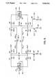
- FIG. 5a schematic diagram of an embodiment of the present invention is shown.
- the conventionis used of the bitline conductors referenced in FIG. 4, that is BL A , BL* A , BL B and BL* B .
- All of the transistors used in this embodimentare N channel field effect transistors (FETs). While steps 1-6 are described in detail, a person understanding the description below will be able to understand how the restore and write operations proceed without further explanation.
- Conductors BL A and BL B and BL* A and BL* Bare connected to respective source and drains of FET transistors 20 and 21 respectively, whose gates are driven by timing signals CB L and CB L * respectively.
- Bitline conductor BL Bis connected to a terminal of sense amplifier 22 via the source-drain circuit of FET transistor 23, while bitline conductor BL A is connected to sense amplifier 24 Via FET 25.
- bitline conductor BL* Bis connected to the other terminal of sense amplifier 22 via FET 26 and bitline conductor BL* A is connected to the other terminal of sense amplifier 24 via FET 27.
- FETs 23 and 26are operated via a timing signal ISO2 which is applied to their gates, and FETs 25 and 27 are enabled by timing signal ISO1 applied to their gates.
- Bitline precharge voltage V BLPis applied to bitlines BL* A and BL A via FETs 28 and 29, and to bitline conductors BL* B and BL B via FETs 30 and 31.
- the charge to be sensedis stored on cell capacitor 32, which is connected to bitline BL A via FET 33, which is driven by the timing signal WL1 received from a word line applied to its gate.
- bitline portionsare isolated from each other by the C BL and C BL* timing voltage being low rendering FETs 20 and 21 non-conductive, and precharge voltage is applied to the four bitline conductors via transistors 28, 29, 30 and 31 due to timing voltages M A1 , M A1* , M A2 and M A2* being high.
- bitline conductor voltagesare equalized via FETs 39 and 34 short-circuiting bitline conductor pairs BL A and BL *A , and BL B and BL *B respectively, FET 39 being enabled by the E Q1 timing voltage being applied to its gate, FET 34 being enabled by E Q2 .
- timing voltages E Q1 , E Q2 and M A1 , M A2 and M A2*go low, causing transistors 39, 34, 29, 31 and 30 to open.
- Timing voltage M A1*remains high, maintaining precharge voltage (V ref2 in step 1 of FIG. 3) on bitline conductor B L*A .
- the next stepis for the timing voltage C BL to go high for a short interval and at the same time for W L1 to go high.
- Thiscauses FET 20 to conduct, connecting bitline conductors BL A and BL B together, and at the same time transistor 33 conducts, causing the charge from bit storage capacitor 32 to be dumped to the bitline conductor BL A . Since the timing voltages ISO1 and lSO2 are low, the transistors 25, 27, 23 and 26 are open, isolating the sense amplifiers 24 and 22 from the bitlines.
- step 1The stage of step 1 in which the cell charge from capacitor 32 is dumped onto the bitline conductors BL A and BL B and that the remaining bitline conductors BL* A and BL *B have been precharged to a midpoint reference voltage V BLP (V ref2 ) has thus been completed.
- the C BL timing voltagereturns to a low level, isolating the bitline conductors BL A and BL B and following this the ISO2 voltage goes high, enabling transistors 23 and 26.
- the timing voltages V S2 and V R2flip, causing sense amplifier 22 to sense the bit stored on bitline conductor B LB relative to the midpoint reference voltage stored on bitline B L*B .
- the full logic level value of the sensed bit (0 or 1)is then applied by sense amplifier 22 to the bitline.
- Timing voltage W L2 going highenables FET 35, causing the sensed bit logic level voltage to be stored in dummy capacitor cell 36.
- step 2wherein the bit has been sensed and stored in the dummy cell capacitor 36.
- the timing voltage ISO2then drops, causing transistors 23 and 26 to isolate the bitline conductors BL B and BL *B from sense amplifier 22.
- the timing voltages EQ2, M A2 and M A2*then go high, causing transistor 34 to conduct and short-circuiting bitline conductors BL B and BL *B , and causing FETs 31 and 30 to conduct, allowing reference voltage V BLP (V ref2 ) to be reapplied to the bitline conductors BL B and BL *B .
- V ref2reference voltage
- the timing voltage C BL*goes high, causing transistor 21 to conduct, joining bitline conductors BL *A with BL *B and BL B .
- V BLPis applied to those three bitline conductors, which are equalized.
- Ccell capacitor 37is then connected to the bitline conductor BL B via FET 38 due to the gate of FET 38 going high with the timing voltage V CL . This completes operation through to the completion of step 3 described with reference to FIG. 3.
- timing voltage M A2 and M A2* , as well as M A1*then go to low level, inhibiting FETs 31, 30 and 28, cutting off reference voltage V BLP from the bitline conductors.
- the next stepis for the timing voltage WL2 to go high. This causes the charge stored on dummy cell capacitor 36 to be dumped onto the three interconnected bitline conductors BL B , BL *B and BL A , and as well onto Ccell 37. This completes step 4 described with reference to FIG. 3.
- the timing voltage EQ2then drops to low level, removing the short circuit between the bitline conductors BL B and BL *B , and the timing voltage C BL* drops to low level, causing separation of the bitline conductors BL *A and BL *B .
- the four bitline conductorsare thus mutually isolated.
- the timing voltage M A2*then goes to high level for a short period, recharging the bitline conductor B L*B to the reference voltage V BLP .
- the result, at this stage,is that the bitline conductor B L*B is at the voltage of reference level V BLP , the bitline conductors B L*A and BL B are charged to the distributed level resulting from the charge previously stored on dummy capacitor 36, and the bitline conductor B LA is charged to the level stored on the bit storage cell capacitor 32. This completes step 5 described with reference to FIG. 3.
- the timing voltages ISO1 and ISO2then go to high level, enabling FETs 23 and 26, and 25 and 27, thus connecting sense amplifiers 22 and 24 to the bitlines.
- the timing voltages V S1 and V S2 and V R1 and V R2are inverted, causing operation of sense amplifiers 22 and 24, thus sensing the bit stored on the two bitlines BL A and BL *B relative to the voltages (which are at the same voltage level) on bitline conductors BL *A and BL B . This completes the operation of step 6 described with reference to FIG. 3.
- bit storage capacitor 32there are several ways of expanding the above invention so that more than four charge levels stored on bit storage capacitor 32 can be detected.
- One wayis to use a variable reference voltage V BLP , which is changed in the direction of the sensed bit level following either a first or successive sensing steps.
- a second wayis to use more than the three voltage reference levels 1/6 V DD , 1/2 V DD , and 5/6 V DD described.
- the bitlinesmay be divided into three sections for three successive sensing operations to get 8 levels, 4 sections or 16 levels, etc.
Landscapes
- Engineering & Computer Science (AREA)
- Computer Hardware Design (AREA)
- Dram (AREA)
Abstract
Description
______________________________________ STORAGE REFERENCE ACTUAL VOLTAGES VOLTAGES VOLTAGE ______________________________________ V.sub.cell1 V.sub.DD V.sub.ref3 5/6 V.sub.DD V.sub.cell2 2/3 V.sub.DD V.sub.ref2 1/2 V.sub.DD V.sub.cell1 1/3 V.sub.DD V.sub.ref1 1/6 V.sub.DD V.sub.cell0 V.sub.SS ______________________________________
Claims (9)
Priority Applications (3)
| Application Number | Priority Date | Filing Date | Title |
|---|---|---|---|
| US07/916,673US5283761A (en) | 1992-07-22 | 1992-07-22 | Method of multi-level storage in DRAM |
| US08/595,020USRE37072E1 (en) | 1992-07-22 | 1996-01-31 | Method of multi-level storage in DRAM and apparatus thereof |
| US09/654,367USRE40075E1 (en) | 1992-07-22 | 2000-09-01 | Method of multi-level storage in DRAM and apparatus thereof |
Applications Claiming Priority (1)
| Application Number | Priority Date | Filing Date | Title |
|---|---|---|---|
| US07/916,673US5283761A (en) | 1992-07-22 | 1992-07-22 | Method of multi-level storage in DRAM |
Related Parent Applications (1)
| Application Number | Title | Priority Date | Filing Date |
|---|---|---|---|
| US08/595,020ContinuationUSRE37072E1 (en) | 1992-07-22 | 1996-01-31 | Method of multi-level storage in DRAM and apparatus thereof |
Related Child Applications (2)
| Application Number | Title | Priority Date | Filing Date |
|---|---|---|---|
| US08/595,020ReissueUSRE37072E1 (en) | 1992-07-22 | 1996-01-31 | Method of multi-level storage in DRAM and apparatus thereof |
| US09/654,367ReissueUSRE40075E1 (en) | 1992-07-22 | 2000-09-01 | Method of multi-level storage in DRAM and apparatus thereof |
Publications (1)
| Publication Number | Publication Date |
|---|---|
| US5283761Atrue US5283761A (en) | 1994-02-01 |
Family
ID=25437664
Family Applications (2)
| Application Number | Title | Priority Date | Filing Date |
|---|---|---|---|
| US07/916,673CeasedUS5283761A (en) | 1992-07-22 | 1992-07-22 | Method of multi-level storage in DRAM |
| US08/595,020Expired - LifetimeUSRE37072E1 (en) | 1992-07-22 | 1996-01-31 | Method of multi-level storage in DRAM and apparatus thereof |
Family Applications After (1)
| Application Number | Title | Priority Date | Filing Date |
|---|---|---|---|
| US08/595,020Expired - LifetimeUSRE37072E1 (en) | 1992-07-22 | 1996-01-31 | Method of multi-level storage in DRAM and apparatus thereof |
Country Status (1)
| Country | Link |
|---|---|
| US (2) | US5283761A (en) |
Cited By (112)
| Publication number | Priority date | Publication date | Assignee | Title |
|---|---|---|---|---|
| US5410508A (en)* | 1993-05-14 | 1995-04-25 | Micron Semiconductor, Inc. | Pumped wordlines |
| WO1995034075A1 (en)* | 1994-06-02 | 1995-12-14 | Intel Corporation | Sensing schemes for flash memory with multilevel cells |
| US5532955A (en)* | 1994-12-30 | 1996-07-02 | Mosaid Technologies Incorporated | Method of multilevel dram sense and restore |
| US5539695A (en)* | 1995-01-23 | 1996-07-23 | Solidas Corporation | Fast access multi-bit random access memory |
| US5539690A (en)* | 1994-06-02 | 1996-07-23 | Intel Corporation | Write verify schemes for flash memory with multilevel cells |
| US5594691A (en)* | 1995-02-15 | 1997-01-14 | Intel Corporation | Address transition detection sensing interface for flash memory having multi-bit cells |
| US5650976A (en)* | 1993-05-14 | 1997-07-22 | Micron Technology, Inc. | Dual strobed negative pumped wordlines for dynamic random access memories |
| US5684736A (en)* | 1996-06-17 | 1997-11-04 | Nuram Technology, Inc. | Multilevel memory cell sense amplifier system |
| US5694143A (en)* | 1994-06-02 | 1997-12-02 | Accelerix Limited | Single chip frame buffer and graphics accelerator |
| US5761110A (en)* | 1996-12-23 | 1998-06-02 | Lsi Logic Corporation | Memory cell capable of storing more than two logic states by using programmable resistances |
| US5761114A (en)* | 1997-02-19 | 1998-06-02 | International Business Machines Corporation | Multi-level storage gain cell with stepline |
| US5771187A (en)* | 1996-12-23 | 1998-06-23 | Lsi Logic Corporation | Multiple level storage DRAM cell |
| US5781472A (en)* | 1994-06-02 | 1998-07-14 | Intel Corporation | Bit map addressing schemes for flash/memory |
| US5784328A (en)* | 1996-12-23 | 1998-07-21 | Lsi Logic Corporation | Memory system including an on-chip temperature sensor for regulating the refresh rate of a DRAM array |
| US5808932A (en)* | 1996-12-23 | 1998-09-15 | Lsi Logic Corporation | Memory system which enables storage and retrieval of more than two states in a memory cell |
| US5815107A (en)* | 1996-12-19 | 1998-09-29 | International Business Machines Corporation | Current source referenced high speed analog to digitial converter |
| US5847990A (en)* | 1996-12-23 | 1998-12-08 | Lsi Logic Corporation | Ram cell capable of storing 3 logic states |
| US5892710A (en)* | 1994-01-21 | 1999-04-06 | Intel Corporation | Method and circuitry for storing discrete amounts of charge in a single memory element |
| US5909404A (en)* | 1998-03-27 | 1999-06-01 | Lsi Logic Corporation | Refresh sampling built-in self test and repair circuit |
| US5923276A (en)* | 1996-12-19 | 1999-07-13 | International Business Machines Corporation | Current source based multilevel bus driver and converter |
| US5956350A (en)* | 1997-10-27 | 1999-09-21 | Lsi Logic Corporation | Built in self repair for DRAMs using on-chip temperature sensing and heating |
| US5982659A (en)* | 1996-12-23 | 1999-11-09 | Lsi Logic Corporation | Memory cell capable of storing more than two logic states by using different via resistances |
| US6016268A (en)* | 1997-02-18 | 2000-01-18 | Richard Mann | Three transistor multi-state dynamic memory cell for embedded CMOS logic applications |
| US6041010A (en)* | 1994-06-20 | 2000-03-21 | Neomagic Corporation | Graphics controller integrated circuit without memory interface pins and associated power dissipation |
| US6101561A (en)* | 1998-02-06 | 2000-08-08 | International Business Machines Corporation | System for providing an increase in digital data transmission rate over a parallel bus by converting binary format voltages to encoded analog format currents |
| US6137739A (en)* | 1998-06-29 | 2000-10-24 | Hyundai Electronics Industries Co., Ltd. | Multilevel sensing circuit and method thereof |
| US6282145B1 (en) | 1999-01-14 | 2001-08-28 | Silicon Storage Technology, Inc. | Array architecture and operating methods for digital multilevel nonvolatile memory integrated circuit system |
| US6285598B1 (en) | 1997-03-06 | 2001-09-04 | Silicon Storage Technology, Inc. | Precision programming of nonvolatile memory cells |
| US6292395B1 (en) | 1999-12-30 | 2001-09-18 | Macronix International Co., Ltd. | Source and drain sensing |
| US6396742B1 (en) | 2000-07-28 | 2002-05-28 | Silicon Storage Technology, Inc. | Testing of multilevel semiconductor memory |
| US6462986B1 (en)* | 1995-10-06 | 2002-10-08 | Silicon Storage Technology, Inc. | Integrated circuit for storage and retrieval of multiple digital bits per nonvolatile memory cell |
| US6487116B2 (en) | 1997-03-06 | 2002-11-26 | Silicon Storage Technology, Inc. | Precision programming of nonvolatile memory cells |
| US6556469B2 (en) | 1999-05-26 | 2003-04-29 | Gershom Birk | System and method for multilevel DRAM sensing and restoring |
| US6587372B2 (en) | 2001-01-11 | 2003-07-01 | Micron Technology, Inc. | Memory device with multi-level storage cells and apparatuses, systems and methods including same |
| US20030179615A1 (en)* | 2001-01-11 | 2003-09-25 | Blodgett Greg A. | Memory device with multi-level storage cells and apparatuses, systems and methods including same |
| US20040059845A1 (en)* | 2002-09-25 | 2004-03-25 | Samsung Electronics Co., Ltd. | Simultaneous bidirectional input/output circuit |
| US20050099879A1 (en)* | 2002-03-18 | 2005-05-12 | Matthias Goldbach | Circuit arrangement for reading out, evaluating and reading in again a charge state into a memory cell |
| US20050174841A1 (en)* | 2004-02-05 | 2005-08-11 | Iota Technology, Inc. | Electronic memory with tri-level cell pair |
| US20060034130A1 (en)* | 2004-08-16 | 2006-02-16 | Bo Liu | Low power, high speed read method for a multi-level cell DRAM |
| US20060083098A1 (en)* | 2004-02-05 | 2006-04-20 | Iota Technology, Inc. | Electronic memory with binary storage elements |
| US20060245282A1 (en)* | 2003-10-09 | 2006-11-02 | Jung Chul M | Sense amplifier circuit |
| US20070195619A1 (en)* | 2006-02-21 | 2007-08-23 | Samsung Electronics Co., Ltd. | Integrated circuit memory devices having multi-bit normal memory cells and single-bit redundant memory cells therein |
| USRE40075E1 (en)* | 1992-07-22 | 2008-02-19 | Mosaid Technologies, Incorporated | Method of multi-level storage in DRAM and apparatus thereof |
| US20110007565A1 (en)* | 1996-09-18 | 2011-01-13 | Katsuki Hazama | Multilevel semiconductor memory, write/read method thereto/therefrom and storage medium storing write/read program |
| KR20130141512A (en)* | 2010-10-20 | 2013-12-26 | 가부시키가이샤 한도오따이 에네루기 켄큐쇼 | Method of driving semiconductor device |
| US20140063915A1 (en)* | 2010-12-30 | 2014-03-06 | Kandou Labs, SA | Differential vector storage for dynamic random access memory |
| US9203402B1 (en) | 2010-05-20 | 2015-12-01 | Kandou Labs SA | Efficient processing and detection of balanced codes |
| US9246713B2 (en) | 2010-05-20 | 2016-01-26 | Kandou Labs, S.A. | Vector signaling with reduced receiver complexity |
| US9251873B1 (en) | 2010-05-20 | 2016-02-02 | Kandou Labs, S.A. | Methods and systems for pin-efficient memory controller interface using vector signaling codes for chip-to-chip communications |
| US9258154B2 (en) | 2014-02-02 | 2016-02-09 | Kandou Labs, S.A. | Method and apparatus for low power chip-to-chip communications with constrained ISI ratio |
| US9268683B1 (en) | 2012-05-14 | 2016-02-23 | Kandou Labs, S.A. | Storage method and apparatus for random access memory using codeword storage |
| US9288089B2 (en) | 2010-04-30 | 2016-03-15 | Ecole Polytechnique Federale De Lausanne (Epfl) | Orthogonal differential vector signaling |
| US9288082B1 (en) | 2010-05-20 | 2016-03-15 | Kandou Labs, S.A. | Circuits for efficient detection of vector signaling codes for chip-to-chip communication using sums of differences |
| US9300503B1 (en) | 2010-05-20 | 2016-03-29 | Kandou Labs, S.A. | Methods and systems for skew tolerance in and advanced detectors for vector signaling codes for chip-to-chip communication |
| US9357036B2 (en) | 2010-05-20 | 2016-05-31 | Kandou Labs, S.A. | Methods and systems for chip-to-chip communication with reduced simultaneous switching noise |
| US9362962B2 (en) | 2010-05-20 | 2016-06-07 | Kandou Labs, S.A. | Methods and systems for energy-efficient communications interface |
| US9362974B2 (en) | 2010-05-20 | 2016-06-07 | Kandou Labs, S.A. | Methods and systems for high bandwidth chip-to-chip communications interface |
| US9363114B2 (en) | 2014-02-28 | 2016-06-07 | Kandou Labs, S.A. | Clock-embedded vector signaling codes |
| US9362947B2 (en) | 2010-12-30 | 2016-06-07 | Kandou Labs, S.A. | Sorting decoder |
| US9369312B1 (en) | 2014-02-02 | 2016-06-14 | Kandou Labs, S.A. | Low EMI signaling for parallel conductor interfaces |
| US9401828B2 (en) | 2010-05-20 | 2016-07-26 | Kandou Labs, S.A. | Methods and systems for low-power and pin-efficient communications with superposition signaling codes |
| US9419828B2 (en) | 2013-11-22 | 2016-08-16 | Kandou Labs, S.A. | Multiwire linear equalizer for vector signaling code receiver |
| US9419564B2 (en) | 2014-05-16 | 2016-08-16 | Kandou Labs, S.A. | Symmetric linear equalization circuit with increased gain |
| US9432082B2 (en) | 2014-07-17 | 2016-08-30 | Kandou Labs, S.A. | Bus reversable orthogonal differential vector signaling codes |
| US9444654B2 (en) | 2014-07-21 | 2016-09-13 | Kandou Labs, S.A. | Multidrop data transfer |
| US9450744B2 (en) | 2010-05-20 | 2016-09-20 | Kandou Lab, S.A. | Control loop management and vector signaling code communications links |
| US9461862B2 (en) | 2014-08-01 | 2016-10-04 | Kandou Labs, S.A. | Orthogonal differential vector signaling codes with embedded clock |
| US9478277B1 (en)* | 2015-09-03 | 2016-10-25 | Bo Liu | Tri-level-cell DRAM and sense amplifier with alternating offset voltage |
| US9479369B1 (en) | 2010-05-20 | 2016-10-25 | Kandou Labs, S.A. | Vector signaling codes with high pin-efficiency for chip-to-chip communication and storage |
| US9509437B2 (en) | 2014-05-13 | 2016-11-29 | Kandou Labs, S.A. | Vector signaling code with improved noise margin |
| US9544015B2 (en) | 2014-06-25 | 2017-01-10 | Kandou Labs, S.A. | Multilevel driver for high speed chip-to-chip communications |
| US9557760B1 (en) | 2015-10-28 | 2017-01-31 | Kandou Labs, S.A. | Enhanced phase interpolation circuit |
| US9564994B2 (en) | 2010-05-20 | 2017-02-07 | Kandou Labs, S.A. | Fault tolerant chip-to-chip communication with advanced voltage |
| US9577815B1 (en) | 2015-10-29 | 2017-02-21 | Kandou Labs, S.A. | Clock data alignment system for vector signaling code communications link |
| US9596109B2 (en) | 2010-05-20 | 2017-03-14 | Kandou Labs, S.A. | Methods and systems for high bandwidth communications interface |
| US9660024B2 (en) | 2014-12-18 | 2017-05-23 | Samsung Electronics Co., Ltd. | Semiconductor device with two transistors and a capacitor |
| US9667379B2 (en) | 2010-06-04 | 2017-05-30 | Ecole Polytechnique Federale De Lausanne (Epfl) | Error control coding for orthogonal differential vector signaling |
| US9674014B2 (en) | 2014-10-22 | 2017-06-06 | Kandou Labs, S.A. | Method and apparatus for high speed chip-to-chip communications |
| US9806761B1 (en) | 2014-01-31 | 2017-10-31 | Kandou Labs, S.A. | Methods and systems for reduction of nearest-neighbor crosstalk |
| US9825723B2 (en) | 2010-05-20 | 2017-11-21 | Kandou Labs, S.A. | Methods and systems for skew tolerance in and advanced detectors for vector signaling codes for chip-to-chip communication |
| US9832046B2 (en) | 2015-06-26 | 2017-11-28 | Kandou Labs, S.A. | High speed communications system |
| US9852806B2 (en) | 2014-06-20 | 2017-12-26 | Kandou Labs, S.A. | System for generating a test pattern to detect and isolate stuck faults for an interface using transition coding |
| US9900186B2 (en) | 2014-07-10 | 2018-02-20 | Kandou Labs, S.A. | Vector signaling codes with increased signal to noise characteristics |
| US9906358B1 (en) | 2016-08-31 | 2018-02-27 | Kandou Labs, S.A. | Lock detector for phase lock loop |
| US9972371B2 (en) | 2016-06-20 | 2018-05-15 | Samsung Electronics Co., Ltd. | Memory device including memory cell for generating reference voltage |
| US9985745B2 (en) | 2013-06-25 | 2018-05-29 | Kandou Labs, S.A. | Vector signaling with reduced receiver complexity |
| US9985634B2 (en) | 2010-05-20 | 2018-05-29 | Kandou Labs, S.A. | Data-driven voltage regulator |
| US10003454B2 (en) | 2016-04-22 | 2018-06-19 | Kandou Labs, S.A. | Sampler with low input kickback |
| US10003315B2 (en) | 2016-01-25 | 2018-06-19 | Kandou Labs S.A. | Voltage sampler driver with enhanced high-frequency gain |
| US10057049B2 (en) | 2016-04-22 | 2018-08-21 | Kandou Labs, S.A. | High performance phase locked loop |
| US10056903B2 (en) | 2016-04-28 | 2018-08-21 | Kandou Labs, S.A. | Low power multilevel driver |
| US10055372B2 (en) | 2015-11-25 | 2018-08-21 | Kandou Labs, S.A. | Orthogonal differential vector signaling codes with embedded clock |
| US10091035B2 (en) | 2013-04-16 | 2018-10-02 | Kandou Labs, S.A. | Methods and systems for high bandwidth communications interface |
| US10116468B1 (en) | 2017-06-28 | 2018-10-30 | Kandou Labs, S.A. | Low power chip-to-chip bidirectional communications |
| US10153591B2 (en) | 2016-04-28 | 2018-12-11 | Kandou Labs, S.A. | Skew-resistant multi-wire channel |
| US10200218B2 (en) | 2016-10-24 | 2019-02-05 | Kandou Labs, S.A. | Multi-stage sampler with increased gain |
| US10200188B2 (en) | 2016-10-21 | 2019-02-05 | Kandou Labs, S.A. | Quadrature and duty cycle error correction in matrix phase lock loop |
| US10203226B1 (en) | 2017-08-11 | 2019-02-12 | Kandou Labs, S.A. | Phase interpolation circuit |
| US10277431B2 (en) | 2016-09-16 | 2019-04-30 | Kandou Labs, S.A. | Phase rotation circuit for eye scope measurements |
| US10326623B1 (en) | 2017-12-08 | 2019-06-18 | Kandou Labs, S.A. | Methods and systems for providing multi-stage distributed decision feedback equalization |
| US10333741B2 (en) | 2016-04-28 | 2019-06-25 | Kandou Labs, S.A. | Vector signaling codes for densely-routed wire groups |
| US10372665B2 (en) | 2016-10-24 | 2019-08-06 | Kandou Labs, S.A. | Multiphase data receiver with distributed DFE |
| US10467177B2 (en) | 2017-12-08 | 2019-11-05 | Kandou Labs, S.A. | High speed memory interface |
| US10497428B2 (en) | 2017-12-18 | 2019-12-03 | Samsung Electronics Co., Ltd. | Bit line sense amplifier, semiconductor memory device and multi bit data sensing method thereof |
| US10554380B2 (en) | 2018-01-26 | 2020-02-04 | Kandou Labs, S.A. | Dynamically weighted exclusive or gate having weighted output segments for phase detection and phase interpolation |
| US10686583B2 (en) | 2017-07-04 | 2020-06-16 | Kandou Labs, S.A. | Method for measuring and correcting multi-wire skew |
| US20200211620A1 (en)* | 2018-12-26 | 2020-07-02 | Micron Technology, Inc. | Sensing techniques using a charge transfer device |
| US10706911B1 (en) | 2018-10-10 | 2020-07-07 | Samsung Electronics Co., Ltd. | Sense amplifier for sensing multi-level cell and memory device including the sense amplifier |
| US10985162B2 (en) | 2018-12-14 | 2021-04-20 | John Bennett | System for accurate multiple level gain cells |
| TWI764453B (en)* | 2020-02-05 | 2022-05-11 | 南韓商三星電子股份有限公司 | Volatile memory device and data sensing method thereof |
| US11587688B2 (en) | 2014-03-27 | 2023-02-21 | Raymond Anthony Joao | Apparatus and method for providing healthcare services remotely or virtually with or using an electronic healthcare record and/or a communication network |
| US12340903B2 (en) | 2020-04-14 | 2025-06-24 | Raymond Anthony Joao | Apparatus and method for providing healthcare services remotely or virtually with or using an electronic healthcare record and/or a communication network |
Families Citing this family (2)
| Publication number | Priority date | Publication date | Assignee | Title |
|---|---|---|---|---|
| TW469556B (en)* | 2000-10-16 | 2001-12-21 | United Microelectronics Corp | Wafer burn-in method by using AC timing |
| US8773925B2 (en) | 2010-02-23 | 2014-07-08 | Rambus Inc. | Multilevel DRAM |
Citations (5)
| Publication number | Priority date | Publication date | Assignee | Title |
|---|---|---|---|---|
| US4287570A (en)* | 1979-06-01 | 1981-09-01 | Intel Corporation | Multiple bit read-only memory cell and its sense amplifier |
| US4415992A (en)* | 1981-02-25 | 1983-11-15 | Motorola, Inc. | Memory system having memory cells capable of storing more than two states |
| US4661929A (en)* | 1983-12-23 | 1987-04-28 | Hitachi, Ltd. | Semiconductor memory having multiple level storage structure |
| US4771404A (en)* | 1984-09-05 | 1988-09-13 | Nippon Telegraph And Telephone Corporation | Memory device employing multilevel storage circuits |
| US5184324A (en)* | 1990-12-20 | 1993-02-02 | Sharp Kabushiki Kaisha | Dynamic semiconductor multi-value memory device |
Family Cites Families (2)
| Publication number | Priority date | Publication date | Assignee | Title |
|---|---|---|---|---|
| JPS59203298A (en) | 1983-05-04 | 1984-11-17 | Nec Corp | Semiconductor memory |
| US5293563A (en) | 1988-12-29 | 1994-03-08 | Sharp Kabushiki Kaisha | Multi-level memory cell with increased read-out margin |
- 1992
- 1992-07-22USUS07/916,673patent/US5283761A/ennot_activeCeased
- 1996
- 1996-01-31USUS08/595,020patent/USRE37072E1/ennot_activeExpired - Lifetime
Patent Citations (5)
| Publication number | Priority date | Publication date | Assignee | Title |
|---|---|---|---|---|
| US4287570A (en)* | 1979-06-01 | 1981-09-01 | Intel Corporation | Multiple bit read-only memory cell and its sense amplifier |
| US4415992A (en)* | 1981-02-25 | 1983-11-15 | Motorola, Inc. | Memory system having memory cells capable of storing more than two states |
| US4661929A (en)* | 1983-12-23 | 1987-04-28 | Hitachi, Ltd. | Semiconductor memory having multiple level storage structure |
| US4771404A (en)* | 1984-09-05 | 1988-09-13 | Nippon Telegraph And Telephone Corporation | Memory device employing multilevel storage circuits |
| US5184324A (en)* | 1990-12-20 | 1993-02-02 | Sharp Kabushiki Kaisha | Dynamic semiconductor multi-value memory device |
Cited By (199)
| Publication number | Priority date | Publication date | Assignee | Title |
|---|---|---|---|---|
| USRE40075E1 (en)* | 1992-07-22 | 2008-02-19 | Mosaid Technologies, Incorporated | Method of multi-level storage in DRAM and apparatus thereof |
| US5636175A (en)* | 1993-05-14 | 1997-06-03 | Micron Semiconductor, Inc. | Row decoder/driver circuit for determining non selected wordlines and for driving non-selected wordlines to a potential less than the lowest potential of the digit lines |
| US5410508A (en)* | 1993-05-14 | 1995-04-25 | Micron Semiconductor, Inc. | Pumped wordlines |
| US5926433A (en)* | 1993-05-14 | 1999-07-20 | Micron Technology, Inc. | Dual strobed negative pumped worldlines for dynamic random access memories |
| US5650976A (en)* | 1993-05-14 | 1997-07-22 | Micron Technology, Inc. | Dual strobed negative pumped wordlines for dynamic random access memories |
| US5892710A (en)* | 1994-01-21 | 1999-04-06 | Intel Corporation | Method and circuitry for storing discrete amounts of charge in a single memory element |
| US6091618A (en)* | 1994-01-21 | 2000-07-18 | Intel Corporation | Method and circuitry for storing discrete amounts of charge in a single memory element |
| US5694143A (en)* | 1994-06-02 | 1997-12-02 | Accelerix Limited | Single chip frame buffer and graphics accelerator |
| RU2190260C2 (en)* | 1994-06-02 | 2002-09-27 | Интел Корпорейшн | Reading circuit for flash storage with multilevel cells |
| US5539690A (en)* | 1994-06-02 | 1996-07-23 | Intel Corporation | Write verify schemes for flash memory with multilevel cells |
| US5815443A (en)* | 1994-06-02 | 1998-09-29 | Intel Corporation | Bit map addressing schemes for flash memory |
| US6483742B1 (en) | 1994-06-02 | 2002-11-19 | Intel Corporation | Bit map addressing schemes for flash memory |
| US5748546A (en)* | 1994-06-02 | 1998-05-05 | Intel Corporation | Sensing scheme for flash memory with multilevel cells |
| USRE41565E1 (en) | 1994-06-02 | 2010-08-24 | Mosaid Technologies Incorporated | Single chip frame buffer and graphics accelerator |
| WO1995034075A1 (en)* | 1994-06-02 | 1995-12-14 | Intel Corporation | Sensing schemes for flash memory with multilevel cells |
| USRE37944E1 (en) | 1994-06-02 | 2002-12-31 | 3612821 Canada Inc. | Single chip frame buffer and graphics accelerator |
| US5781472A (en)* | 1994-06-02 | 1998-07-14 | Intel Corporation | Bit map addressing schemes for flash/memory |
| USRE44589E1 (en) | 1994-06-02 | 2013-11-12 | Mosaid Technologies Incorporated | Single chip frame buffer and graphics accelerator |
| USRE40326E1 (en) | 1994-06-02 | 2008-05-20 | Mosaid Technologies Incorporated | Single chip frame buffer and graphics accelerator |
| US5828616A (en)* | 1994-06-02 | 1998-10-27 | Intel Corporation | Sensing scheme for flash memory with multilevel cells |
| US7106619B2 (en) | 1994-06-20 | 2006-09-12 | Neomagic Corporation | Graphics controller integrated circuit without memory interface |
| US6356497B1 (en) | 1994-06-20 | 2002-03-12 | Neomagic Corporation | Graphics controller integrated circuit without memory interface |
| US6920077B2 (en) | 1994-06-20 | 2005-07-19 | Neomagic Corporation | Graphics controller integrated circuit without memory interface |
| US20040179015A1 (en)* | 1994-06-20 | 2004-09-16 | Neomagic Corporation | Graphics controller integrated circuit without memory interface |
| US20060208764A1 (en)* | 1994-06-20 | 2006-09-21 | Puar Deepraj S | Graphics Controller Integrated Circuit without Memory Interface |
| US6041010A (en)* | 1994-06-20 | 2000-03-21 | Neomagic Corporation | Graphics controller integrated circuit without memory interface pins and associated power dissipation |
| US5532955A (en)* | 1994-12-30 | 1996-07-02 | Mosaid Technologies Incorporated | Method of multilevel dram sense and restore |
| EP0720176A3 (en)* | 1994-12-30 | 1998-01-14 | Mosaid Technologies Incorporated | Method of multilevel dram sense and restore |
| US5612912A (en)* | 1994-12-30 | 1997-03-18 | Mosaid Technologies Incorporated | Method of multilevel DRAM sense and restore |
| US5539695A (en)* | 1995-01-23 | 1996-07-23 | Solidas Corporation | Fast access multi-bit random access memory |
| US5594691A (en)* | 1995-02-15 | 1997-01-14 | Intel Corporation | Address transition detection sensing interface for flash memory having multi-bit cells |
| US6462986B1 (en)* | 1995-10-06 | 2002-10-08 | Silicon Storage Technology, Inc. | Integrated circuit for storage and retrieval of multiple digital bits per nonvolatile memory cell |
| US5684736A (en)* | 1996-06-17 | 1997-11-04 | Nuram Technology, Inc. | Multilevel memory cell sense amplifier system |
| US5859794A (en)* | 1996-06-17 | 1999-01-12 | Nuram Technology, Inc. | Multilevel memory cell sense amplifier system and sensing methods |
| US20110007565A1 (en)* | 1996-09-18 | 2011-01-13 | Katsuki Hazama | Multilevel semiconductor memory, write/read method thereto/therefrom and storage medium storing write/read program |
| US8707130B2 (en)* | 1996-09-18 | 2014-04-22 | Intellectual Ventures I Llc | Multilevel semiconductor memory, write/read method thereto/therefrom and storage medium storing write/read program |
| US5923276A (en)* | 1996-12-19 | 1999-07-13 | International Business Machines Corporation | Current source based multilevel bus driver and converter |
| US5815107A (en)* | 1996-12-19 | 1998-09-29 | International Business Machines Corporation | Current source referenced high speed analog to digitial converter |
| US5847990A (en)* | 1996-12-23 | 1998-12-08 | Lsi Logic Corporation | Ram cell capable of storing 3 logic states |
| US5761110A (en)* | 1996-12-23 | 1998-06-02 | Lsi Logic Corporation | Memory cell capable of storing more than two logic states by using programmable resistances |
| US5771187A (en)* | 1996-12-23 | 1998-06-23 | Lsi Logic Corporation | Multiple level storage DRAM cell |
| US5784328A (en)* | 1996-12-23 | 1998-07-21 | Lsi Logic Corporation | Memory system including an on-chip temperature sensor for regulating the refresh rate of a DRAM array |
| US5982659A (en)* | 1996-12-23 | 1999-11-09 | Lsi Logic Corporation | Memory cell capable of storing more than two logic states by using different via resistances |
| US5808932A (en)* | 1996-12-23 | 1998-09-15 | Lsi Logic Corporation | Memory system which enables storage and retrieval of more than two states in a memory cell |
| US6016268A (en)* | 1997-02-18 | 2000-01-18 | Richard Mann | Three transistor multi-state dynamic memory cell for embedded CMOS logic applications |
| US5761114A (en)* | 1997-02-19 | 1998-06-02 | International Business Machines Corporation | Multi-level storage gain cell with stepline |
| US6487116B2 (en) | 1997-03-06 | 2002-11-26 | Silicon Storage Technology, Inc. | Precision programming of nonvolatile memory cells |
| US6285598B1 (en) | 1997-03-06 | 2001-09-04 | Silicon Storage Technology, Inc. | Precision programming of nonvolatile memory cells |
| US5956350A (en)* | 1997-10-27 | 1999-09-21 | Lsi Logic Corporation | Built in self repair for DRAMs using on-chip temperature sensing and heating |
| US6101561A (en)* | 1998-02-06 | 2000-08-08 | International Business Machines Corporation | System for providing an increase in digital data transmission rate over a parallel bus by converting binary format voltages to encoded analog format currents |
| US5909404A (en)* | 1998-03-27 | 1999-06-01 | Lsi Logic Corporation | Refresh sampling built-in self test and repair circuit |
| US6137739A (en)* | 1998-06-29 | 2000-10-24 | Hyundai Electronics Industries Co., Ltd. | Multilevel sensing circuit and method thereof |
| US6282145B1 (en) | 1999-01-14 | 2001-08-28 | Silicon Storage Technology, Inc. | Array architecture and operating methods for digital multilevel nonvolatile memory integrated circuit system |
| US8432750B2 (en) | 1999-01-14 | 2013-04-30 | Silicon Storage Technology, Inc. | Non-volatile memory systems and methods including page read and/or configuration features |
| US7471581B2 (en) | 1999-01-14 | 2008-12-30 | Silicon Storage Technology, Inc. | Wide dynamic range and high speed voltage mode sensing for a multilevel digital non-volatile memory |
| US20090147579A1 (en)* | 1999-01-14 | 2009-06-11 | Silicon Storage Technology, Inc. | Non-volatile memory systems and methods including page read and/or configuration features |
| US9640263B2 (en) | 1999-01-14 | 2017-05-02 | Silicon Storage Technology, Inc. | Non-volatile memory systems and methods |
| US7848159B2 (en) | 1999-01-14 | 2010-12-07 | Silicon Storage Technology, Inc. | Non-volatile memory systems and methods including page read and/or configuration features |
| US8614924B2 (en) | 1999-01-14 | 2013-12-24 | Silicon Storage Technology, Inc. | Non-volatile memory systems and methods |
| US20070159904A1 (en)* | 1999-01-14 | 2007-07-12 | Tran Hieu V | Wide dynamic range and high speed voltage mode sensing for a multilevel digital non-volatile memory |
| US20110110170A1 (en)* | 1999-01-14 | 2011-05-12 | Hieu Van Tran | Non-volatile memory systems and methods including page read and/or configuration features |
| US6556469B2 (en) | 1999-05-26 | 2003-04-29 | Gershom Birk | System and method for multilevel DRAM sensing and restoring |
| US6292395B1 (en) | 1999-12-30 | 2001-09-18 | Macronix International Co., Ltd. | Source and drain sensing |
| US6404678B1 (en) | 1999-12-30 | 2002-06-11 | Macronix International Co., Ltd. | Source and drain sensing |
| US6396742B1 (en) | 2000-07-28 | 2002-05-28 | Silicon Storage Technology, Inc. | Testing of multilevel semiconductor memory |
| US6587372B2 (en) | 2001-01-11 | 2003-07-01 | Micron Technology, Inc. | Memory device with multi-level storage cells and apparatuses, systems and methods including same |
| US20030179615A1 (en)* | 2001-01-11 | 2003-09-25 | Blodgett Greg A. | Memory device with multi-level storage cells and apparatuses, systems and methods including same |
| US6816408B2 (en)* | 2001-01-11 | 2004-11-09 | Micron Technology, Inc. | Memory device with multi-level storage cells |
| US20030202396A1 (en)* | 2001-01-11 | 2003-10-30 | Blodgett Greg A. | Memory device with multi-level storage cells |
| US6654280B2 (en) | 2001-01-11 | 2003-11-25 | Micron Technology, Inc. | Memory device with multi-level storage cells |
| US6901007B2 (en) | 2001-01-11 | 2005-05-31 | Micron Technology, Inc. | Memory device with multi-level storage cells and apparatuses, systems and methods including same |
| US7009900B2 (en) | 2002-03-18 | 2006-03-07 | Infineon Technologies Ag | Circuit arrangement for reading out, evaluating and reading in again a charge state into a memory cell |
| US20050099879A1 (en)* | 2002-03-18 | 2005-05-12 | Matthias Goldbach | Circuit arrangement for reading out, evaluating and reading in again a charge state into a memory cell |
| US7102545B2 (en)* | 2002-09-25 | 2006-09-05 | Samsung Electronics Co., Ltd. | Simultaneous bidirectional input/output circuit |
| US20040059845A1 (en)* | 2002-09-25 | 2004-03-25 | Samsung Electronics Co., Ltd. | Simultaneous bidirectional input/output circuit |
| US20060245282A1 (en)* | 2003-10-09 | 2006-11-02 | Jung Chul M | Sense amplifier circuit |
| US7606088B2 (en)* | 2003-10-09 | 2009-10-20 | Micron Technology, Inc. | Sense amplifier circuit |
| US7433250B2 (en)* | 2003-10-09 | 2008-10-07 | Micron Technology, Inc. | Sense amplifier circuit |
| US20090040854A1 (en)* | 2003-10-09 | 2009-02-12 | Micron Technology, Inc. | Sense amplifier circuit |
| US7352619B2 (en) | 2004-02-05 | 2008-04-01 | Iota Technology, Inc. | Electronic memory with binary storage elements |
| US20060083098A1 (en)* | 2004-02-05 | 2006-04-20 | Iota Technology, Inc. | Electronic memory with binary storage elements |
| US20050174841A1 (en)* | 2004-02-05 | 2005-08-11 | Iota Technology, Inc. | Electronic memory with tri-level cell pair |
| US7133311B2 (en)* | 2004-08-16 | 2006-11-07 | Bo Liu | Low power, high speed read method for a multi-level cell DRAM |
| US20060034130A1 (en)* | 2004-08-16 | 2006-02-16 | Bo Liu | Low power, high speed read method for a multi-level cell DRAM |
| US20070195619A1 (en)* | 2006-02-21 | 2007-08-23 | Samsung Electronics Co., Ltd. | Integrated circuit memory devices having multi-bit normal memory cells and single-bit redundant memory cells therein |
| US9825677B2 (en) | 2010-04-30 | 2017-11-21 | ECOLE POLYTECHNIQUE FéDéRALE DE LAUSANNE | Orthogonal differential vector signaling |
| US9288089B2 (en) | 2010-04-30 | 2016-03-15 | Ecole Polytechnique Federale De Lausanne (Epfl) | Orthogonal differential vector signaling |
| US9203402B1 (en) | 2010-05-20 | 2015-12-01 | Kandou Labs SA | Efficient processing and detection of balanced codes |
| US9985634B2 (en) | 2010-05-20 | 2018-05-29 | Kandou Labs, S.A. | Data-driven voltage regulator |
| US10468078B2 (en) | 2010-05-20 | 2019-11-05 | Kandou Labs, S.A. | Methods and systems for pin-efficient memory controller interface using vector signaling codes for chip-to-chip communication |
| US9596109B2 (en) | 2010-05-20 | 2017-03-14 | Kandou Labs, S.A. | Methods and systems for high bandwidth communications interface |
| US9607673B1 (en) | 2010-05-20 | 2017-03-28 | Kandou Labs S.A. | Methods and systems for pin-efficient memory controller interface using vector signaling codes for chip-to-chip communication |
| US9246713B2 (en) | 2010-05-20 | 2016-01-26 | Kandou Labs, S.A. | Vector signaling with reduced receiver complexity |
| US9288082B1 (en) | 2010-05-20 | 2016-03-15 | Kandou Labs, S.A. | Circuits for efficient detection of vector signaling codes for chip-to-chip communication using sums of differences |
| US9300503B1 (en) | 2010-05-20 | 2016-03-29 | Kandou Labs, S.A. | Methods and systems for skew tolerance in and advanced detectors for vector signaling codes for chip-to-chip communication |
| US9357036B2 (en) | 2010-05-20 | 2016-05-31 | Kandou Labs, S.A. | Methods and systems for chip-to-chip communication with reduced simultaneous switching noise |
| US9362962B2 (en) | 2010-05-20 | 2016-06-07 | Kandou Labs, S.A. | Methods and systems for energy-efficient communications interface |
| US9362974B2 (en) | 2010-05-20 | 2016-06-07 | Kandou Labs, S.A. | Methods and systems for high bandwidth chip-to-chip communications interface |
| US9564994B2 (en) | 2010-05-20 | 2017-02-07 | Kandou Labs, S.A. | Fault tolerant chip-to-chip communication with advanced voltage |
| US9577664B2 (en) | 2010-05-20 | 2017-02-21 | Kandou Labs, S.A. | Efficient processing and detection of balanced codes |
| US9686107B2 (en) | 2010-05-20 | 2017-06-20 | Kandou Labs, S.A. | Methods and systems for chip-to-chip communication with reduced simultaneous switching noise |
| US10044452B2 (en) | 2010-05-20 | 2018-08-07 | Kandou Labs, S.A. | Methods and systems for skew tolerance in and advanced detectors for vector signaling codes for chip-to-chip communication |
| US9401828B2 (en) | 2010-05-20 | 2016-07-26 | Kandou Labs, S.A. | Methods and systems for low-power and pin-efficient communications with superposition signaling codes |
| US9413384B1 (en) | 2010-05-20 | 2016-08-09 | Kandou Labs, S.A. | Efficient processing and detection of balanced codes |
| US9251873B1 (en) | 2010-05-20 | 2016-02-02 | Kandou Labs, S.A. | Methods and systems for pin-efficient memory controller interface using vector signaling codes for chip-to-chip communications |
| US9929818B2 (en) | 2010-05-20 | 2018-03-27 | Kandou Bus, S.A. | Methods and systems for selection of unions of vector signaling codes for power and pin efficient chip-to-chip communication |
| US9692555B2 (en) | 2010-05-20 | 2017-06-27 | Kandou Labs, S.A. | Vector signaling with reduced receiver complexity |
| US9838017B2 (en) | 2010-05-20 | 2017-12-05 | Kandou Labs, S.A. | Methods and systems for high bandwidth chip-to-chip communcations interface |
| US9825723B2 (en) | 2010-05-20 | 2017-11-21 | Kandou Labs, S.A. | Methods and systems for skew tolerance in and advanced detectors for vector signaling codes for chip-to-chip communication |
| US9450791B2 (en) | 2010-05-20 | 2016-09-20 | Kandoub Lab, S.A. | Circuits for efficient detection of vector signaling codes for chip-to-chip communication |
| US9450744B2 (en) | 2010-05-20 | 2016-09-20 | Kandou Lab, S.A. | Control loop management and vector signaling code communications links |
| US9485057B2 (en) | 2010-05-20 | 2016-11-01 | Kandou Labs, S.A. | Vector signaling with reduced receiver complexity |
| US9819522B2 (en) | 2010-05-20 | 2017-11-14 | Kandou Labs, S.A. | Circuits for efficient detection of vector signaling codes for chip-to-chip communication |
| US9479369B1 (en) | 2010-05-20 | 2016-10-25 | Kandou Labs, S.A. | Vector signaling codes with high pin-efficiency for chip-to-chip communication and storage |
| US9667379B2 (en) | 2010-06-04 | 2017-05-30 | Ecole Polytechnique Federale De Lausanne (Epfl) | Error control coding for orthogonal differential vector signaling |
| KR20130141512A (en)* | 2010-10-20 | 2013-12-26 | 가부시키가이샤 한도오따이 에네루기 켄큐쇼 | Method of driving semiconductor device |
| KR101989392B1 (en) | 2010-10-20 | 2019-06-14 | 가부시키가이샤 한도오따이 에네루기 켄큐쇼 | Method for driving semiconductor deivce |
| US9424908B2 (en)* | 2010-12-30 | 2016-08-23 | Kandou Labs, S.A. | Differential vector storage for dynamic random access memory |
| US9362947B2 (en) | 2010-12-30 | 2016-06-07 | Kandou Labs, S.A. | Sorting decoder |
| US10164809B2 (en) | 2010-12-30 | 2018-12-25 | Kandou Labs, S.A. | Circuits for efficient detection of vector signaling codes for chip-to-chip communication |
| US20140063915A1 (en)* | 2010-12-30 | 2014-03-06 | Kandou Labs, SA | Differential vector storage for dynamic random access memory |
| US9275720B2 (en)* | 2010-12-30 | 2016-03-01 | Kandou Labs, S.A. | Differential vector storage for dynamic random access memory |
| US9361223B1 (en) | 2012-05-14 | 2016-06-07 | Kandou Labs, S.A. | Storage method and apparatus for random access memory using codeword storage |
| US9524106B1 (en) | 2012-05-14 | 2016-12-20 | Kandou Labs, S.A. | Storage method and apparatus for random access memory using codeword storage |
| US9268683B1 (en) | 2012-05-14 | 2016-02-23 | Kandou Labs, S.A. | Storage method and apparatus for random access memory using codeword storage |
| US10091035B2 (en) | 2013-04-16 | 2018-10-02 | Kandou Labs, S.A. | Methods and systems for high bandwidth communications interface |
| US9985745B2 (en) | 2013-06-25 | 2018-05-29 | Kandou Labs, S.A. | Vector signaling with reduced receiver complexity |
| US9419828B2 (en) | 2013-11-22 | 2016-08-16 | Kandou Labs, S.A. | Multiwire linear equalizer for vector signaling code receiver |
| US10177812B2 (en) | 2014-01-31 | 2019-01-08 | Kandou Labs, S.A. | Methods and systems for reduction of nearest-neighbor crosstalk |
| US9806761B1 (en) | 2014-01-31 | 2017-10-31 | Kandou Labs, S.A. | Methods and systems for reduction of nearest-neighbor crosstalk |
| US9258154B2 (en) | 2014-02-02 | 2016-02-09 | Kandou Labs, S.A. | Method and apparatus for low power chip-to-chip communications with constrained ISI ratio |
| US9369312B1 (en) | 2014-02-02 | 2016-06-14 | Kandou Labs, S.A. | Low EMI signaling for parallel conductor interfaces |
| US9686106B2 (en) | 2014-02-28 | 2017-06-20 | Kandou Labs, S.A. | Clock-embedded vector signaling codes |
| US10020966B2 (en) | 2014-02-28 | 2018-07-10 | Kandou Labs, S.A. | Vector signaling codes with high pin-efficiency for chip-to-chip communication and storage |
| US10374846B2 (en) | 2014-02-28 | 2019-08-06 | Kandou Labs, S.A. | Clock-embedded vector signaling codes |
| US10805129B2 (en) | 2014-02-28 | 2020-10-13 | Kandou Labs, S.A. | Clock-embedded vector signaling codes |
| US9363114B2 (en) | 2014-02-28 | 2016-06-07 | Kandou Labs, S.A. | Clock-embedded vector signaling codes |
| US11587688B2 (en) | 2014-03-27 | 2023-02-21 | Raymond Anthony Joao | Apparatus and method for providing healthcare services remotely or virtually with or using an electronic healthcare record and/or a communication network |
| US9509437B2 (en) | 2014-05-13 | 2016-11-29 | Kandou Labs, S.A. | Vector signaling code with improved noise margin |
| US10333749B2 (en) | 2014-05-13 | 2019-06-25 | Kandou Labs, S.A. | Vector signaling code with improved noise margin |
| US9419564B2 (en) | 2014-05-16 | 2016-08-16 | Kandou Labs, S.A. | Symmetric linear equalization circuit with increased gain |
| US9692381B2 (en) | 2014-05-16 | 2017-06-27 | Kandou Labs, S.A. | Symmetric linear equalization circuit with increased gain |
| US9852806B2 (en) | 2014-06-20 | 2017-12-26 | Kandou Labs, S.A. | System for generating a test pattern to detect and isolate stuck faults for an interface using transition coding |
| US10091033B2 (en) | 2014-06-25 | 2018-10-02 | Kandou Labs, S.A. | Multilevel driver for high speed chip-to-chip communications |
| US9544015B2 (en) | 2014-06-25 | 2017-01-10 | Kandou Labs, S.A. | Multilevel driver for high speed chip-to-chip communications |
| US9917711B2 (en) | 2014-06-25 | 2018-03-13 | Kandou Labs, S.A. | Multilevel driver for high speed chip-to-chip communications |
| US9900186B2 (en) | 2014-07-10 | 2018-02-20 | Kandou Labs, S.A. | Vector signaling codes with increased signal to noise characteristics |
| US10320588B2 (en) | 2014-07-10 | 2019-06-11 | Kandou Labs, S.A. | Vector signaling codes with increased signal to noise characteristics |
| US10003424B2 (en) | 2014-07-17 | 2018-06-19 | Kandou Labs, S.A. | Bus reversible orthogonal differential vector signaling codes |
| US9432082B2 (en) | 2014-07-17 | 2016-08-30 | Kandou Labs, S.A. | Bus reversable orthogonal differential vector signaling codes |
| US9444654B2 (en) | 2014-07-21 | 2016-09-13 | Kandou Labs, S.A. | Multidrop data transfer |
| US9893911B2 (en) | 2014-07-21 | 2018-02-13 | Kandou Labs, S.A. | Multidrop data transfer |
| US10230549B2 (en) | 2014-07-21 | 2019-03-12 | Kandou Labs, S.A. | Multidrop data transfer |
| US9461862B2 (en) | 2014-08-01 | 2016-10-04 | Kandou Labs, S.A. | Orthogonal differential vector signaling codes with embedded clock |
| US10122561B2 (en) | 2014-08-01 | 2018-11-06 | Kandou Labs, S.A. | Orthogonal differential vector signaling codes with embedded clock |
| US9838234B2 (en) | 2014-08-01 | 2017-12-05 | Kandou Labs, S.A. | Orthogonal differential vector signaling codes with embedded clock |
| US9674014B2 (en) | 2014-10-22 | 2017-06-06 | Kandou Labs, S.A. | Method and apparatus for high speed chip-to-chip communications |
| US10243765B2 (en) | 2014-10-22 | 2019-03-26 | Kandou Labs, S.A. | Method and apparatus for high speed chip-to-chip communications |
| US9660024B2 (en) | 2014-12-18 | 2017-05-23 | Samsung Electronics Co., Ltd. | Semiconductor device with two transistors and a capacitor |
| US9832046B2 (en) | 2015-06-26 | 2017-11-28 | Kandou Labs, S.A. | High speed communications system |
| US10116472B2 (en) | 2015-06-26 | 2018-10-30 | Kandou Labs, S.A. | High speed communications system |
| US9478277B1 (en)* | 2015-09-03 | 2016-10-25 | Bo Liu | Tri-level-cell DRAM and sense amplifier with alternating offset voltage |
| DE112016004005T5 (en) | 2015-09-03 | 2018-07-12 | Shenzhen Xingmem Technology Corporation | Three-level dynamic random access memory and method of reading the same |
| DE112016004005B4 (en) | 2015-09-03 | 2020-06-04 | Shenzhen Xingmem Technology Corporation | Dynamic three-level cell random access memory and method for reading the same |
| TWI576840B (en)* | 2015-09-03 | 2017-04-01 | 深圳星憶存儲科技有限公司 | Tri-level-cell dram and method for reading out the same |
| CN106409328A (en)* | 2015-09-03 | 2017-02-15 | 深圳星忆存储科技有限公司 | Dynamic random access memory for three-level unit, and method for reading same |
| CN106409328B (en)* | 2015-09-03 | 2018-05-18 | 深圳星忆存储科技有限公司 | The dynamic random access memory and its read method of three-level cells |
| US9557760B1 (en) | 2015-10-28 | 2017-01-31 | Kandou Labs, S.A. | Enhanced phase interpolation circuit |
| US9577815B1 (en) | 2015-10-29 | 2017-02-21 | Kandou Labs, S.A. | Clock data alignment system for vector signaling code communications link |
| US10055372B2 (en) | 2015-11-25 | 2018-08-21 | Kandou Labs, S.A. | Orthogonal differential vector signaling codes with embedded clock |
| US10003315B2 (en) | 2016-01-25 | 2018-06-19 | Kandou Labs S.A. | Voltage sampler driver with enhanced high-frequency gain |
| US10003454B2 (en) | 2016-04-22 | 2018-06-19 | Kandou Labs, S.A. | Sampler with low input kickback |
| US10057049B2 (en) | 2016-04-22 | 2018-08-21 | Kandou Labs, S.A. | High performance phase locked loop |
| US10153591B2 (en) | 2016-04-28 | 2018-12-11 | Kandou Labs, S.A. | Skew-resistant multi-wire channel |
| US10056903B2 (en) | 2016-04-28 | 2018-08-21 | Kandou Labs, S.A. | Low power multilevel driver |
| US10333741B2 (en) | 2016-04-28 | 2019-06-25 | Kandou Labs, S.A. | Vector signaling codes for densely-routed wire groups |
| US10332571B2 (en)* | 2016-06-20 | 2019-06-25 | Samsung Electronics Co., Ltd. | Memory device including memory cell for generating reference voltage |
| US9972371B2 (en) | 2016-06-20 | 2018-05-15 | Samsung Electronics Co., Ltd. | Memory device including memory cell for generating reference voltage |
| US20180233183A1 (en)* | 2016-06-20 | 2018-08-16 | Samsung Electronics Co., Ltd. | Memory device including memory cell for generating reference voltage |
| US10355852B2 (en) | 2016-08-31 | 2019-07-16 | Kandou Labs, S.A. | Lock detector for phase lock loop |
| US9906358B1 (en) | 2016-08-31 | 2018-02-27 | Kandou Labs, S.A. | Lock detector for phase lock loop |
| US10277431B2 (en) | 2016-09-16 | 2019-04-30 | Kandou Labs, S.A. | Phase rotation circuit for eye scope measurements |
| US10200188B2 (en) | 2016-10-21 | 2019-02-05 | Kandou Labs, S.A. | Quadrature and duty cycle error correction in matrix phase lock loop |
| US10200218B2 (en) | 2016-10-24 | 2019-02-05 | Kandou Labs, S.A. | Multi-stage sampler with increased gain |
| US10372665B2 (en) | 2016-10-24 | 2019-08-06 | Kandou Labs, S.A. | Multiphase data receiver with distributed DFE |
| US10116468B1 (en) | 2017-06-28 | 2018-10-30 | Kandou Labs, S.A. | Low power chip-to-chip bidirectional communications |
| US10686583B2 (en) | 2017-07-04 | 2020-06-16 | Kandou Labs, S.A. | Method for measuring and correcting multi-wire skew |
| US10203226B1 (en) | 2017-08-11 | 2019-02-12 | Kandou Labs, S.A. | Phase interpolation circuit |
| US10326623B1 (en) | 2017-12-08 | 2019-06-18 | Kandou Labs, S.A. | Methods and systems for providing multi-stage distributed decision feedback equalization |
| US10467177B2 (en) | 2017-12-08 | 2019-11-05 | Kandou Labs, S.A. | High speed memory interface |
| US10497428B2 (en) | 2017-12-18 | 2019-12-03 | Samsung Electronics Co., Ltd. | Bit line sense amplifier, semiconductor memory device and multi bit data sensing method thereof |
| US10554380B2 (en) | 2018-01-26 | 2020-02-04 | Kandou Labs, S.A. | Dynamically weighted exclusive or gate having weighted output segments for phase detection and phase interpolation |
| US10706911B1 (en) | 2018-10-10 | 2020-07-07 | Samsung Electronics Co., Ltd. | Sense amplifier for sensing multi-level cell and memory device including the sense amplifier |
| US10854277B2 (en) | 2018-10-10 | 2020-12-01 | Samsung Electronics Co., Ltd. | Sense amplifier for sensing multi-level cell and memory device including the sense amplifer |
| US10985162B2 (en) | 2018-12-14 | 2021-04-20 | John Bennett | System for accurate multiple level gain cells |
| US20200211620A1 (en)* | 2018-12-26 | 2020-07-02 | Micron Technology, Inc. | Sensing techniques using a charge transfer device |
| TWI764453B (en)* | 2020-02-05 | 2022-05-11 | 南韓商三星電子股份有限公司 | Volatile memory device and data sensing method thereof |
| US11501824B2 (en) | 2020-02-05 | 2022-11-15 | Samsung Electronics Co., Ltd. | Volatile memory device and data sensing method thereof |
| US12340903B2 (en) | 2020-04-14 | 2025-06-24 | Raymond Anthony Joao | Apparatus and method for providing healthcare services remotely or virtually with or using an electronic healthcare record and/or a communication network |
Also Published As
| Publication number | Publication date |
|---|---|
| USRE37072E1 (en) | 2001-02-27 |
Similar Documents
| Publication | Publication Date | Title |
|---|---|---|
| US5283761A (en) | Method of multi-level storage in DRAM | |
| US5532955A (en) | Method of multilevel dram sense and restore | |
| USRE41351E1 (en) | CAM arrays having CAM cells therein with match line and low match line connections and methods of operating same | |
| US4841483A (en) | Semiconductor memory | |
| US5339274A (en) | Variable bitline precharge voltage sensing technique for DRAM structures | |
| US6373765B1 (en) | Method for multilevel DRAM sensing | |
| US5724286A (en) | Flexible DRAM array | |
| US5093808A (en) | Folded bitline dynamic ram with reduced shared supply voltages | |
| EP0833340A1 (en) | Reading circuit for semiconductor memory cells | |
| US5233560A (en) | Dynamic memory bit line precharge scheme | |
| JP4643092B2 (en) | Improved multi-layer DRAM | |
| US4648073A (en) | Sequential shared access lines memory cells | |
| US4598387A (en) | Capacitive memory signal doubler cell | |
| EP0676767B1 (en) | Dram page copy method | |
| US5771187A (en) | Multiple level storage DRAM cell | |
| US5563831A (en) | Timing reference circuit for bitline precharge in memory arrays | |
| USRE40075E1 (en) | Method of multi-level storage in DRAM and apparatus thereof | |
| US4719600A (en) | Sense circuit for multilevel storage system | |
| JPH01192083A (en) | Semiconductor memory | |
| JPH08180688A (en) | Semiconductor memory | |
| US6018486A (en) | Reading method and circuit for dynamic memory | |
| US6671218B2 (en) | System and method for hiding refresh cycles in a dynamic type content addressable memory | |
| US5894443A (en) | Static semiconductor memory device capable of reducing precharging power dissipation | |
| JPH03194789A (en) | Semiconductor memory device | |
| JPH04283490A (en) | Semiconductor storage device |
Legal Events
| Date | Code | Title | Description |
|---|---|---|---|
| AS | Assignment | Owner name:MOSAID TECHNOLOGIES INCORPORATED, CANADA Free format text:ASSIGNMENT OF ASSIGNORS INTEREST.;ASSIGNOR:GILLINGHAM, PETER B.;REEL/FRAME:006207/0646 Effective date:19920707 | |
| STCF | Information on status: patent grant | Free format text:PATENTED CASE | |
| RF | Reissue application filed | Effective date:19960131 | |
| FPAY | Fee payment | Year of fee payment:4 | |
| RF | Reissue application filed | Effective date:20000901 | |
| AS | Assignment | Owner name:MOSAID TECHNOLOGIES INCORPORATED,CANADA Free format text:CHANGE OF REGISTERED OFFICE ADDRESS;ASSIGNOR:MOSAID TECHNOLOGIES INCORPORATED;REEL/FRAME:024286/0805 Effective date:20090209 Owner name:MOSAID TECHNOLOGIES INCORPORATED,CANADA Free format text:CHANGE-CORRECTION OF NAME AND ADDRESS;ASSIGNOR:MOSAID TECHNOLOGIES INCORPORATED;REEL/FRAME:024286/0800 Effective date:20091117 | |
| FEPP | Fee payment procedure | Free format text:PAYOR NUMBER ASSIGNED (ORIGINAL EVENT CODE: ASPN); ENTITY STATUS OF PATENT OWNER: SMALL ENTITY Free format text:PAYER NUMBER DE-ASSIGNED (ORIGINAL EVENT CODE: RMPN); ENTITY STATUS OF PATENT OWNER: SMALL ENTITY | |
| AS | Assignment | Owner name:ROYAL BANK OF CANADA, CANADA Free format text:U.S. INTELLECTUAL PROPERTY SECURITY AGREEMENT (FOR NON-U.S. GRANTORS) - SHORT FORM;ASSIGNORS:658276 N.B. LTD.;658868 N.B. INC.;MOSAID TECHNOLOGIES INCORPORATED;REEL/FRAME:027512/0196 Effective date:20111223 |