US5282196A - Bursted and non-bursted data router - Google Patents
Bursted and non-bursted data routerDownload PDFInfo
- Publication number
- US5282196A US5282196AUS07/776,942US77694291AUS5282196AUS 5282196 AUS5282196 AUS 5282196AUS 77694291 AUS77694291 AUS 77694291AUS 5282196 AUS5282196 AUS 5282196A
- Authority
- US
- United States
- Prior art keywords
- data
- bursted
- input
- buffer means
- output
- Prior art date
- Legal status (The legal status is an assumption and is not a legal conclusion. Google has not performed a legal analysis and makes no representation as to the accuracy of the status listed.)
- Expired - Lifetime
Links
- 239000000872bufferSubstances0.000claimsabstractdescription132
- 238000013519translationMethods0.000claimsabstractdescription6
- 230000015654memoryEffects0.000claimsdescription82
- 238000000034methodMethods0.000claimsdescription6
- 230000015572biosynthetic processEffects0.000claims3
- 238000010586diagramMethods0.000description23
- 238000004891communicationMethods0.000description6
- 238000012545processingMethods0.000description4
- 238000013461designMethods0.000description3
- 238000012986modificationMethods0.000description3
- 230000004048modificationEffects0.000description3
- 230000036316preloadEffects0.000description3
- 230000005540biological transmissionEffects0.000description2
- 238000011094buffer selectionMethods0.000description2
- 125000004122cyclic groupChemical group0.000description2
- 230000006870functionEffects0.000description2
- 230000000295complement effectEffects0.000description1
- 239000008358core componentSubstances0.000description1
- 230000005055memory storageEffects0.000description1
- 230000000630rising effectEffects0.000description1
- 230000001360synchronised effectEffects0.000description1
Images


Classifications
- H—ELECTRICITY
- H04—ELECTRIC COMMUNICATION TECHNIQUE
- H04J—MULTIPLEX COMMUNICATION
- H04J3/00—Time-division multiplex systems
- H04J3/02—Details
- H04J3/06—Synchronising arrangements
- H04J3/062—Synchronisation of signals having the same nominal but fluctuating bit rates, e.g. using buffers
- H04J3/0626—Synchronisation of signals having the same nominal but fluctuating bit rates, e.g. using buffers plesiochronous multiplexing systems, e.g. plesiochronous digital hierarchy [PDH], jitter attenuators
- H—ELECTRICITY
- H04—ELECTRIC COMMUNICATION TECHNIQUE
- H04Q—SELECTING
- H04Q11/00—Selecting arrangements for multiplex systems
- H04Q11/04—Selecting arrangements for multiplex systems for time-division multiplexing
- H—ELECTRICITY
- H04—ELECTRIC COMMUNICATION TECHNIQUE
- H04Q—SELECTING
- H04Q11/00—Selecting arrangements for multiplex systems
- H04Q11/04—Selecting arrangements for multiplex systems for time-division multiplexing
- H04Q11/0428—Integrated services digital network, i.e. systems for transmission of different types of digitised signals, e.g. speech, data, telecentral, television signals
- H04Q11/0478—Provisions for broadband connections
- H—ELECTRICITY
- H04—ELECTRIC COMMUNICATION TECHNIQUE
- H04J—MULTIPLEX COMMUNICATION
- H04J2203/00—Aspects of optical multiplex systems other than those covered by H04J14/05 and H04J14/07
- H04J2203/0001—Provisions for broadband connections in integrated services digital network using frames of the Optical Transport Network [OTN] or using synchronous transfer mode [STM], e.g. SONET, SDH
- H04J2203/0003—Switching fabrics, e.g. transport network, control network
- H04J2203/0005—Switching elements
- H—ELECTRICITY
- H04—ELECTRIC COMMUNICATION TECHNIQUE
- H04J—MULTIPLEX COMMUNICATION
- H04J2203/00—Aspects of optical multiplex systems other than those covered by H04J14/05 and H04J14/07
- H04J2203/0001—Provisions for broadband connections in integrated services digital network using frames of the Optical Transport Network [OTN] or using synchronous transfer mode [STM], e.g. SONET, SDH
- H04J2203/0089—Multiplexing, e.g. coding, scrambling, SONET
Definitions
- the present inventionrelates to communication systems. More specifically, the present invention relates to data routing systems.
- a data routeris a device that accepts data in one or more formats from one or more input channels and routes the data to one or more output channels in one or more formats.
- a bursted data routeris a data router with input and output channels formatted into groups of data symbols called bursts. Bursts are usually grouped into time-division multiplexed frames, with each burst in a frame numbered from 1 to N, for purposes of routing identification.
- Routingtakes place when a burst is moved from its source, e.g., input channel 1, 2 or 3 and input burst number 1 to N, to its destination, e.g., output channel 1 or 2 and output burst number 1 to N.
- each channelmay carry different types of bursts, with each burst type having a characteristic length (number of symbols per burst) and period (time duration of each burst).
- Output burstsmay be constructed of one or more input bursts, or just a fraction of an input burst.
- a bursted data routermust translate incoming data bursts into the required output burst format.
- Input channelsprovide formatted data bursts to the router and output channels from the router provide formatted data bursts to connected communications devices such as transmission lines, modulators, and eventually to demultiplexers.
- One router output channelmay eventually connect to many communications devices.
- Demultiplexers connected to the router outputexamine a specific area of a frame to extract the burst carrying data of interest. These devices generally expect the burst to be in a specific format.
- the routertherefore functions as a multi-position switch and format translator, directing input data to its desired destination device and translating it into a specified format.
- Bursted data routerstake advantage of the known, predetermined period of each input burst to simplify routing. A small range of acceptable, selectable burst periods, lengths and timing are determined during router design. Typically, incoming bursts are timed such that their boundaries (where they start and stop in time) are aligned. By aligning incoming burst boundaries, access of each input burst to an output channel can be precisely and simply scheduled to avoid conflicts with other bursts. All incoming bursts arriving during the same burst period are accumulated in burst-sized input buffers. During the following burst period, the input buffers take turns accessing (transferring their data to) output channels. Each input buffer is assigned a fixed time interval within a burst period in which to access the output channels. Thus, collisions between two input bursts simultaneously trying to access the same output channel are avoided.
- the need in the artis addressed by the present invention which in a most general sense is a data router for receiving input data, having a timing characteristic, and transmitting output data that is either bursted or non-bursted.
- the non-bursted datacomprises frames of data with each frame comprising slots of data, each slot having a position and a number.
- the inventionprovides translation between bursted and non-bursted formats and includes an input buffer circuit for receiving input data from an input channel and storing the input data as the input data is received from the input channel.
- An output buffer circuitis included for formatting the stored input data, translating between bursted and non-bursted data formats and outputting the formatted and translated data to an output channel.
- a sequencer routing controller circuitcontrols the operation of the input buffer circuit and output buffer circuit.
- This inventionallows both bursted and non-bursted data to be freely routed between input and output channels of both types.
- the addition of non-bursted data routing capabilitydoes not interfere with or reduce normal burst routing capabilities.
- This inventionprovides for (1) the time alignment of inconveniently located non-bursted frame boundaries, (2) collision-free scheduling for the routing of irregularly sized and timed groups of data symbols, called slots, and (3) reformatting of slotted data into bursted data.
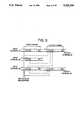
- FIG. 1is a block diagram of an exemplary data router.
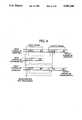
- FIG. 2(a)-2(c)show the structure of an exemplary bursted channel.
- FIG. 2(a)shows multiple frames in a single channel.
- FIG. 2(b)shows an ordered set of bursts within a frame.
- FIG. 2(c)depicts an ordered set of data symbols within a burst with a lead-in of unused dead time shown at D.
- FIG. 3is a simple diagram illustrating the routing of an exemplary burst.
- FIG. 4shows one cycle of a scheduled, cyclic routing process.
- FIG. 5is a block diagram of an exemplary bursted configuration sequencer.
- FIG. 6is a block diagram of an exemplary local reservation memory in an output buffer.
- FIG. 7is a block diagram of an exemplary output buffer local format memory.
- FIG. 8(a)-8(c)are exemplary structures of a non-bursted input channel.
- FIG. 8(a)depicts a single channel carrying multiple frames of non-bursted data.
- FIG. 8(b)shows each non-bursted frame as including a sync word S followed by an ordered set of N slots of varying lengths.
- FIG. 8(c)shows that each slot is composed of an ordered set of data symbols.
- FIG. 9depicts a routing example containing both bursted and non-bursted data.
- FIG. 10shows one cycle of a bursted/non-bursted routing schedule.
- FIGS. 11 and 12are block diagrams of bursted and non-bursted input buffers, respectively.
- FIG. 13illustrates an arrangement for synchronizing incoming non-bursted data to the router master clock using a series of D-type flip-flops.
- FIG. 14illustrates a sync detector utilized in the present invention.
- FIG. 15illustrates detail on the ping-pong buffer implementation of the present invention.
- FIG. 16illustrates a read/write address counter with frame start latch utilized in the present invention.
- FIG. 17shows a slotted frame configuration memory utilized in the present invention.
- FIG. 18is a block diagram of a bursted/non-bursted configuration sequencer utilized in the present invention.
- FIG. 19is an illustrative implementation of a block diagram of a bursted/non-bursted router utilized in the present invention.
- FIG. 20is a block diagram of the non-bursted output buffer utilized in the bursted/non-bursted router of the present invention.
- FIG. 21illustrates various output buffer data processing combinations.
- FIG. 22is a block diagram of a bursted/non-bursted output buffer write address controller block diagram utilized in the present invention.
- FIG. 23is block diagram of a conventional bursted read address controller.
- FIG. 24is a block diagram of a non-bursted read address controller utilized in the present invention.
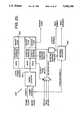
- FIG. 1is a block diagram of an exemplary bursted data router 10.
- the router 10includes a plurality of input burst buffers 14 connected to a respective input channel.
- Each input buffer 14has its output connected to a multiplexed data bus 16.
- Each input buffer 14is shown as a ping-pong buffer.
- input buffersare generally ping-pong in design, so that they can accept incoming channel data while simultaneously transferring previously accumulated data to output channels.
- Ping-pong memory buffersare composed of two physical memory banks; one bank accepts input channel data while the other provides data to an output process. At the end of each burst period the memory banks switch roles and the process continues.
- a plurality of output burst buffers 18each have their input connected to the data bus 16.
- the output buffers 18are also shown as ping-pong buffers.
- the input burst buffers 14are read enabled by a RAM configuration memory 20 and the output burst buffers 18 are write enabled by the RAM configuration memory 20.
- a bursted data router 10is a data router whose input and output channels are formatted into groups of data symbols called bursts. Bursts are usually grouped into time-division multiplexed frames, with each burst in a frame numbered from 1 to N, for purposes of routing identification.
- the structure of an exemplary bursted channelis shown in FIGS. 2(a)-2(c).
- FIG. 2(a)shows multiple frames in a single channel.
- FIG. 2(b)shows an ordered set of bursts within a frame.
- FIG. 2(c)depicts an ordered set of data symbols within a burst with a lead in of unused dead time shown at D.
- routingtakes place when a burst is moved from its source, input channel 1, 2 or 3 and input burst number 1 to N, to its destination, output channel 1 or 2 and output burst number 1 to N.
- each channelmay carry different types of bursts, with each burst type having a characteristic length (number of symbols per burst) and period (time duration of each burst).
- Output burstsmay be constructed of one or more input bursts, or just a fraction of an input burst.
- a bursted data routermust translate incoming data bursts into the required output burst format.
- Input channelsprovide formatted data bursts to the router and output channels from the router provide formatted data bursts to connected communications devices such as transmission lines, modulators, and eventually to demultiplexers.
- One router output channelmay eventually connect to many communications devices.
- Demultiplexers connected to the router outputexamine a specific area of a frame to extract the burst carrying data of interest. These devices generally expect the burst to be in a specific format.
- the routertherefore functions as a multi-position switch and format translator, directing input data to its desired destination device and translating it into a specified format.
- Bursted data routerstake advantage of the known, predetermined period of each input burst to simplify routing. A small range of acceptable, selectable burst periods, lengths and timing are determined during router design. Typically, incoming bursts are timed such that their boundaries (where they start and stop in time) are aligned as shown in FIG. 3. By aligning incoming burst boundaries, access of each input burst to an output channel can be precisely and simply scheduled to avoid conflicts with other bursts. All incoming bursts arriving during the same burst period are accumulated in burst-sized ping-pong input buffers. During the following burst period, the input buffers take turns accessing (transferring their data to) output channels. Each input buffer is assigned a fixed time interval within a burst period in which to access the output channels. Thus, collisions between two input bursts simultaneously accessing the same output channel are avoided. An example of this scheduled, cyclic routing process is shown in FIG. 4.
- Output channelsgenerally accept and store input bursts in a ping-pong frame buffer.
- the frame buffergenerally has specific storage locations reserved for each active input burst of every input channel that occurs in a single input frame.
- Output channel burst storageproceeds for one frame period at the end of which the frame buffer swaps ping and pong memory bank roles and provides the newly stored bursts to channel outputs.
- Output framesare composed and formatted by reading out memory locations in a programmed or hardwired order and rate.
- All routing operationsare generally controlled by the configuration memory 20.
- an address counter 22increments sequentially through each storage address in the configuration memory 20.
- Configuration memory storage locationsgenerally specify a source input buffer and the destination output buffer(s) of a received burst.
- the combination of a configuration memory 20 and address counter 22 controlling this processis commonly called a configuration sequencer 24.
- An example block diagram of a configuration sequenceris given in FIG. 5.
- Each output buffer 18contains a local reservation memory 26 that specifies the correct storage location of a transferred burst.
- An example block diagram of a local reservation memory 26 in an output buffer 18is shown in FIG. 6.
- the output buffer 18will generally use the configuration sequencer address counter 22 as an address to the local reservation memory 26 holding the address in frame memory 28 at which to begin storing the burst. After all input bursts for one frame are stored in frame memory 28, control of the frame memory 28 is transferred to a local frame format memory.
- FIG. 7A block diagram of an exemplary local format memory 30 of an output buffer 18 is shown in FIG. 7.
- a burst counter 32 incrementing sequentially through output frame burst numbersaddresses the local frame format memory 30 which contains the storage location of stored input bursts and their output format. Stored input bursts may be provided to the output channel in any order and format, under the control of the local format memory 30.
- Non-bursted framesgenerally begin with a unique bit pattern called a sync word.
- the sync wordallows the device receiving the non-bursted channel to determine the start of a frame by performing a bit-by-bit compare on the data stream with the expected sync word pattern.
- the frameis divided into groups of data symbols called slots. Unlike bursts, slots can vary in length and duration and may or may not contain dead time at their start.
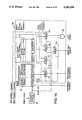
- FIG. 8(a)-8(c)An exemplary structure of a non-bursted input channel is shown in FIG. 8(a)-8(c).
- FIG. 8(a)depicts a single channel carrying multiple frames of non-bursted data.
- FIG. 8(b)shows each nonbursted frame as including a sync word S followed by an ordered set of N slots.
- each slot 100is composed of an ordered set of data symbols. The length and size of the symbols may vary from slot to slot.
- FIG. 9depicts a routing example containing both bursted and non-bursted data. Since non-bursted frame and slot boundaries are not aligned with bursted frame and burst boundaries, it cannot be guaranteed that a slot of data will be fully received before a new routing cycle, begins. (See FIG. 4.)
- the bursted routerexpects that all burst data will be received during a burst period.
- the non-bursted data routercannot guarantee this on non-bursted channels and therefore must have the ability to route partial slots during a routing period. To do so, the non-bursted router must keep track of the slot number it is on, the amount of the slot that has been routed and the number of the next slot to be routed.
- the non-bursted routerWhen the routing of a slot is interrupted by the end of the routing cycle, the non-bursted router must resume routing of the slot during the next cycle. In addition, in some cases, the routing of a slot will be completed during the middle of the access interval assigned to the input channel. In this case, the non-bursted router must select new destinations and begin routing the next slot, without waiting for a new routing cycle.
- a routing schedule example illustrating this situationis shown in FIG. 10.
- FIGS. 11 and 12are block diagrams of a bursted input buffer 102 and a slotted non-bursted input buffer 104, respectively.
- the bursted input buffer 102, of FIG. 11,includes a read/write address counter 109 and ping/pong input buffers 111.
- the non-bursted input buffer 104 of FIG. 12builds on the core components of the bursted input buffer 102, adding a data reclock circuit 106 and sync detector 107, a frame start latch 108 and a slotted frame configuration memory 110.
- the reclock circuit 106synchronizes incoming non-bursted data to the router master clock.
- the data reclock circuitillustrated in FIG. 13, detects a rising edge on the channel clock line when the channel enable is true and generates a reclock enable pulse that is one master clock period in length. Simultaneously, channel data is sampled and reclocked by two flip-flops in series to perform glitch-free synchronization to a router master clock. As shown in FIG. 13, the data reclock circuit 106 is implemented with a series of cascaded D-type flip-flops each of which is clocked by an internal master clock. Channel input data is provided to the input terminal of a first flip-flop 112.
- This signalis clocked through a second flip-flop 114, arranged in cascade with the first flip-flop 112, which provides a "reclock data" signal at the Q output thereof.
- a channel input clock signalis input to a third flip-flop 116.
- This signalis clocked through a fourth flip-flop 118 and a fifth flip-flop 120 connected in cascade.
- the complementary output QN of the fifth flip-flop 120is a first input to an AND gate 122.
- a second input to the AND gate 122is provided by the Q output of the fourth flip-flop 118.
- a channel input enable signalis input to a sixth flip-flop 124.
- This signalis clocked through a seventh flip-flop 126 arranged in cascade with the sixth flip-flop 124.
- the Q output of the seventh flip-flop 126is the third input of the AND gate 122.
- the output of the AND gateis a "reclock enable" signal.
- the reclock data and reclock enable signalsare passed on to the illustrative sync detector 107 of FIG. 14.
- the sync detector 107performs a compare on incoming serial data and detects a specific pattern, (the sync word) that indicates the start of a slotted frame.
- the sync detector 107then pulls the write enable line false to disable storage of the header and sets the header detect line true for one master clock period.
- the net result of this initial processingis to provide a synchronized data stream, stripped of non-payload data headers accompanied by an enable signal that indicates when to store incoming bits.
- the sync detector 107includes a plurality of D type flip-flops arranged in cascade with the input to the first flip-flop 125 being the reclock data signal and the output of the last flip-flop 127 being data.
- the inputs to the flip-flopsare exclusive-ORed (XORed) with a respective bit of the sync word by a series of XOR gates 129.
- the outputs of the XOR gates 129are ANDed by AND gate 128 to provide a header detect signal.
- the header detect signalis counted by a counter 130.
- the output of the header counter 130is ANDed by a second AND gate 132 with the reclock enable signal from the data reclock circuit 106 to provide an enable signal. Both data and enable signals are passed on to the ping-pong buffer 111 of FIG. 12 for storage.
- FIG. 15is a detailed representation of a ping-pong buffer 111.
- the buffer 111includes ping and pong RAM memories 134 and 136, respectively. Read and write addresses are provided to the memories 134 and 136 by address multiplexers 138. Read and write enable signals are provided to the memories 134 and 136 by enable multiplexers 140.
- a tri-state driver 142is connected to the data I/0 input of each memory 134 and 136.
- a ping/pong flagwhich provides read/write control to the pong memory 136, is inverted for input to the ping memory by an inverter 144.
- the read/write address counter 109 of the non-bursted input buffer 104is shown in detail in FIG. 16 with a detailed representation of the frame start latch 108.
- the read/write address counter 109includes a D flip-flop 146, first and second multiplexers 148 and 150, and ping and pong bit counters 152 and 154, respectively.
- the D flip-flop 146is clocked by the burst clock signal and provides the ping/pong flag by the Q output thereof.
- the first and second multiplexers 148 and 150switch the read and write enable signals into the ping and pong bit counters 152 and 154, respectively, under control of the ping/pong flag.
- the outputs of the ping and pong bit counters 152 and 154are input to the frame start latch 108.
- the frame start latch 108includes a first multiplexer 158 which provides the outputs of the bit counters to a latch 160 which stores the address from ping and pong bit counters 152 and 154 respectively where a new frame begins in the ping-pong buffer 111.
- the first multiplexer 158is controlled by the ping/pong flag and the latch 160 is enabled by the header detect signal.
- the output of the latch 160is input to second and third multiplexers 162 and 164, respectively.
- the second input to the second and third multiplexers 162 and 164is provided by the output of the ping and pong bit counters 152 and 154, respectively.
- the outputs of the ping and pong bit countersare the read and write addresses respectively.
- the complimentary output (QN) of the flip-flop 146is fed back to the D input thereof and to the second and third multiplexers 162 and 164 of the frame start latch 108.
- the outputs of the second and third multiplexers 162 and 164are compared by a comparator 166.
- the output of the comparator 166is a start of frame flag.
- the comparator 166detects the start of a new frame by comparing the latched frame start address in the latch, 160, to the current read address from the ping or pong bit counters 152 and 154, respectively, and resets slot offset and slot counters in the slotted frame configuration memory 110 to zero. (See FIGS. 12 and 17.)
- FIG. 17is a detailed representation of the slotted frame configuration memory 110.
- the slotted frame configuration memory 110includes a slot length memory 168, a slot offset counter 170 and a slot counter 172.
- the slot length memory 168contains information about each slot that is loaded sequentially into the slot offset counter 170.
- the slot offset counter 170is then decremented, as each bit is read out of the ping-pong buffer 111, until it reaches zero. Zero indicates the end of a slot and the slot counter 172 is incremented by one.
- the slot counter outputis then used as an address counter to point to the next values in the slot length memory to load into the slot offset counter.
- the values of the slot and slot offset counters 172 and 170are passed to the sequencer routing controller 105 of FIG. 12.
- the bursted/non-bursted configuration sequencer routing controller 105adds to the bursted sequencer 24 of FIG. 5 an additional slot configuration memory 174 for each non-bursted input channel and multiplexers 176-180 to select among bursted and non-bursted memories. During operation, the sequencer 105 will step through each burst configuration word sequentially, at a pace determined by the fixed timing clock.
- the RAM configuration memory 20is modified to contain a slot flag bit which indicates if the input channel currently being processed is slotted. If non-bursted data is being processed, destination selection is placed under the control of the slot configuration memory 174. Unlike the RAM configuration memory 20, the slot configuration word is selected by an address generated from the slot number of an input buffer. In essence, the slotted input buffer keeps track of the slot number it is transferring, informs the sequencer via the slot number line and thereby selects the correct destination for that slot. The sequencer 105 selects the slot number and slot offset from the currently active input buffer and provides this data to the selected output buffer(s) for use in determining where to store the transferred data. The slot offset is set to zero during bursted data transfers. A read enable line both selects the active input buffer and indicates its identity to the selected output buffer(s).
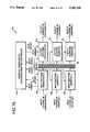
- FIG. 19is a block diagram of the bursted/non-bursted router 200 of the present invention.
- the bursted/non-bursted router 200includes the bursted/non-bursted sequencer routing controller 105, first and second bursted input buffers 102, a non-bursted input buffer 104, bursted output buffers 18 and a non-bursted output buffer 210.
- FIG. 20is a block diagram of the non-bursted output buffer 210 utilized in the bursted/non-bursted router 200 of the present invention.
- the output buffer 210accepts transferred data from the data bus 16 and selection and routing information from the sequencer 105. Note that an output buffer capable of accepting only bursted data requires only the write enable (output buffer selection) signal and the burst number.
- the output buffer 210capable of accepting both bursted and non-bursted data, requires the write enable, burst/slot number and the slot offset.
- the output buffer 210includes a D flip-flop 212, a write address control 214, a read address control 216, a header shift register 218 and a ping-pong memory 111.
- Incoming datais stored at addresses in the ping-pong memory 111 that are determined by the write address control 214. Likewise, data is read out of the ping-pong memory 111 in a specific order by the read address control 216.
- the header shift register 218is used to insert any fixed header information that may be required at the start of an output frame.
- the flip-flop 212 in a toggle configurationis used to perform ping-pong memory buffer selection as controlled by the frame clock.
- the ping-pong memory buffer 111is similar in operation to that used in the input buffers (FIG. 15).
- various combinations of bursted and non-bursted datamay be processed by the output buffer 210, as illustrated in FIG. 21.
- FIG. 22is a block diagram of the write address controller 214 of the output buffer 210.
- the write address controller 214includes a reservation memory 220, an address latch 222, an address counter 224 and an adder 226.
- the address latch 222concatenates the burst/slot number with the source indicator to form an address referencing a location in the reservation memory 220.
- the referenced locationcontains the starting address in the output buffer ping-pong memory at which incoming data will be stored. This starting address is preloaded into the address counter 224 that is then incremented as each data bit is received.
- the counter outputis added to the slot offset from the bursted/non-bursted configuration sequencer, 105, (which is zero for bursted data) and the result is used as a write address for the ping-pong memory 111.
- the adder 226 and slot offsetallow for slots that were incompletely routed during the previous routing period to resume processing at the last address used. Bursted data is, by definition, always completely routed during a routing period and therefore has an offset of zero.
- FIG. 23is a block diagram of a conventional read address controller 216'.
- the read address controller 216'performs formatting of output frames by reading data out of the ping-pong memory in a specific order and with specific timing. On any given output channel, data is either bursted or non-bursted, and each data type requires a different read controller architecture.
- a burst counter 228'increments once for each burst period during a frame period, generating an address to a local format memory 230'.
- the local format memory 230'contains the starting address in the ping-pong memory 111 of an output burst and also an output rate select indicator and a header load flag.
- the starting addressis preloaded into a ping-pong address counter 232' which is then incremented at a rate chosen by the output rate select line.
- the ping-pong address counter 232'provides a read address to the ping-pong memory buffer which outputs the indicated data. If the header flag is true during a burst period, then no data is read out of the ping-pong memory and instead a fixed frame header is inserted.
- Each output bursthas the same duration, but may contain a different number of bits, resulting in an output bit rate that may be different from burst to burst.
- the output bit rateis determined by an output rate clock; each output rate clock corresponds to a specific number of bits in a burst.
- the output rate for each burstis selected by the rate field in the local format memory 230'.
- FIG. 24is a block diagram of the non-bursted read address controller 216.
- the non-bursted read controller 216operates differently than the bursted controller 216'. Unlike bursted frames, non-bursted frames are generally output at a fixed rate and the non-bursted read address controller 216 uses only one output rate clock. Since the output clock is fixed for non-bursted frames, slots containing different numbers of bits have different durations. These durations do not necessarily correspond to burst periods and therefore the burst clock cannot be used to increment the format address counter. Since every slot may be of a different length and hence duration, slot length data is stored in the local format memory for use as a preload into a slot length counter 234.
- the slot length counter 234is decremented as each slot bit is read out.
- the slot length counter 234increments a format address counter 236, enables its own preload, and enables the ping-pong address counter 238 preload.
- the format address counter 236points to an address in the local format memory 230 holding the start address and length of the next slot.
- the ping-pong address counter 238is preloaded with the starting address in the ping-pong memory buffer of a new output slot and begins incrementing at a rate controlled by the output clock. This causes a slot to be read out from the ping-pong memory. In this manner, the read controller 216 formats a frame whose slot boundaries are unrelated to router burst timing.
- the output buffer 210is able to store a slot of data and read it out in a bursted format, or vice versa, according to the choices listed in FIG. 23.
- a significant feature of the inventionis in the non-bursted input buffer which provides resynchronization of incoming data to the master clock, synchronization to the incoming frame and the ability to keep track of the incoming slot number and position in the slot.
- the novel configuration sequencerincludes routing configuration memory space for each non-bursted input channel and circuits to select the non-bursted configuration memory in lieu of the bursted configuration memory when operating on a non-bursted channel.
- the configuration sequenceralso switches slot number and slot offset signals from the input buffer currently being accessed to the output buffer, which uses these signals to determine storage locations.
- the output bufferis composed of three major structures: the write address controller, read address controller and ping-pong memory buffer.
- a write address controller designed for non-bursted datacontrols the storage of either bursted or non-bursted data.
- the read address controlleris designed either for conventional bursted data or for non-bursted data.
- the output buffertranslates between bursted and non-bursted data formats (and vice versa) by reading data into a random access memory (the ping-pong memory buffer) using the natural input timing (bursted or non-bursted) and reading it out using new timing parameters (bursted or non-bursted). By writing data into the memory in one order and reading it out in another, concatenation, splitting and shuffling or deshuffling of data may be performed.
- a significant feature of the inventionis in the manner in which the write addresses in the output buffer are derived.
- input and output buffersare independent.
- non-bursted input buffershelp form the storage address for the output buffer by providing slot and slot offset indicators.
Landscapes
- Engineering & Computer Science (AREA)
- Computer Networks & Wireless Communication (AREA)
- Computer Hardware Design (AREA)
- Signal Processing (AREA)
- Time-Division Multiplex Systems (AREA)
- Data Exchanges In Wide-Area Networks (AREA)
Abstract
Description
Claims (26)
Priority Applications (1)
| Application Number | Priority Date | Filing Date | Title |
|---|---|---|---|
| US07/776,942US5282196A (en) | 1991-10-15 | 1991-10-15 | Bursted and non-bursted data router |
Applications Claiming Priority (1)
| Application Number | Priority Date | Filing Date | Title |
|---|---|---|---|
| US07/776,942US5282196A (en) | 1991-10-15 | 1991-10-15 | Bursted and non-bursted data router |
Publications (1)
| Publication Number | Publication Date |
|---|---|
| US5282196Atrue US5282196A (en) | 1994-01-25 |
Family
ID=25108806
Family Applications (1)
| Application Number | Title | Priority Date | Filing Date |
|---|---|---|---|
| US07/776,942Expired - LifetimeUS5282196A (en) | 1991-10-15 | 1991-10-15 | Bursted and non-bursted data router |
Country Status (1)
| Country | Link |
|---|---|
| US (1) | US5282196A (en) |
Cited By (32)
| Publication number | Priority date | Publication date | Assignee | Title |
|---|---|---|---|---|
| US5521928A (en)* | 1992-11-02 | 1996-05-28 | National Semiconductor Corporation | Time slot exchanger mechanism in a network for data communication having isochronous capability |
| US5537395A (en)* | 1995-04-13 | 1996-07-16 | Northern Telecom Limited | Method and apparatus for setting a channel congestion message in a wireless multiple access packet data system |
| US5781551A (en)* | 1994-09-15 | 1998-07-14 | Texas Instruments Incorporated | Computer communications system with tree architecture and communications method |
| US5805597A (en)* | 1996-06-04 | 1998-09-08 | National Semiconductor Corporation | Method and apparatus for providing low power basic telephony type service over a twisted pair ethernet physical layer |
| WO2001016682A1 (en)* | 1999-08-27 | 2001-03-08 | International Business Machines Corporation | Vlsi network processor and methods |
| US6209020B1 (en)* | 1996-09-20 | 2001-03-27 | Nortel Networks Limited | Distributed pipeline memory architecture for a computer system with even and odd pids |
| US20020075864A1 (en)* | 2000-12-18 | 2002-06-20 | Philips Electronics North America Corp. | Technique for creating a machine to route non-packetized digital signals using distributed RAM |
| US20020105966A1 (en)* | 2000-11-17 | 2002-08-08 | Ronak Patel | Backplane interface adapter with error control and redundant fabric |
| US20050175018A1 (en)* | 2003-05-15 | 2005-08-11 | Wong Yuen F. | System and method for high speed packet transmission implementing dual transmit and receive pipelines |
| US20060222017A1 (en)* | 2005-04-01 | 2006-10-05 | Quiroga Emilio J | Methods and apparatus for synchronizing data transferred across a multi-pin asynchronous serial interface |
| US20070208876A1 (en)* | 2002-05-06 | 2007-09-06 | Davis Ian E | Method and apparatus for efficiently processing data packets in a computer network |
| US20070288690A1 (en)* | 2006-06-13 | 2007-12-13 | Foundry Networks, Inc. | High bandwidth, high capacity look-up table implementation in dynamic random access memory |
| US20070297433A1 (en)* | 2006-06-26 | 2007-12-27 | Mediatek Inc. | Method and apparatus for double buffering |
| US20080002707A1 (en)* | 2002-05-06 | 2008-01-03 | Davis Ian E | Flexible method for processing data packets in a network routing system for enhanced efficiency and monitoring capability |
| US20080049742A1 (en)* | 2006-08-22 | 2008-02-28 | Deepak Bansal | System and method for ecmp load sharing |
| US20090279440A1 (en)* | 2007-01-11 | 2009-11-12 | Foundry Networks, Inc. | Techniques for processing incoming failure detection protocol packets |
| US20090279558A1 (en)* | 2002-05-06 | 2009-11-12 | Ian Edward Davis | Network routing apparatus for enhanced efficiency and monitoring capability |
| US20090279423A1 (en)* | 2006-11-22 | 2009-11-12 | Foundry Networks, Inc. | Recovering from Failures Without Impact on Data Traffic in a Shared Bus Architecture |
| US20090279559A1 (en)* | 2004-03-26 | 2009-11-12 | Foundry Networks, Inc., A Delaware Corporation | Method and apparatus for aggregating input data streams |
| US20090282148A1 (en)* | 2007-07-18 | 2009-11-12 | Foundry Networks, Inc. | Segmented crc design in high speed networks |
| US20090282322A1 (en)* | 2007-07-18 | 2009-11-12 | Foundry Networks, Inc. | Techniques for segmented crc design in high speed networks |
| US20090279561A1 (en)* | 2000-11-17 | 2009-11-12 | Foundry Networks, Inc. | Backplane Interface Adapter |
| US20090279548A1 (en)* | 2002-05-06 | 2009-11-12 | Foundry Networks, Inc. | Pipeline method and system for switching packets |
| US7649885B1 (en) | 2002-05-06 | 2010-01-19 | Foundry Networks, Inc. | Network routing system for enhanced efficiency and monitoring capability |
| US7657703B1 (en)* | 2004-10-29 | 2010-02-02 | Foundry Networks, Inc. | Double density content addressable memory (CAM) lookup scheme |
| US7738450B1 (en) | 2002-05-06 | 2010-06-15 | Foundry Networks, Inc. | System architecture for very fast ethernet blade |
| US8090901B2 (en) | 2009-05-14 | 2012-01-03 | Brocade Communications Systems, Inc. | TCAM management approach that minimize movements |
| US8149839B1 (en) | 2007-09-26 | 2012-04-03 | Foundry Networks, Llc | Selection of trunk ports and paths using rotation |
| US8448162B2 (en) | 2005-12-28 | 2013-05-21 | Foundry Networks, Llc | Hitless software upgrades |
| US8599850B2 (en) | 2009-09-21 | 2013-12-03 | Brocade Communications Systems, Inc. | Provisioning single or multistage networks using ethernet service instances (ESIs) |
| US8730961B1 (en) | 2004-04-26 | 2014-05-20 | Foundry Networks, Llc | System and method for optimizing router lookup |
| US20230283566A1 (en)* | 2020-11-17 | 2023-09-07 | Huawei Technologies Co., Ltd. | Packet processing method and related apparatus |
Citations (7)
| Publication number | Priority date | Publication date | Assignee | Title |
|---|---|---|---|---|
| US4206322A (en)* | 1978-09-25 | 1980-06-03 | Bell Telephone Laboratories, Incorporated | Time-division switching system for multirate data |
| US4207435A (en)* | 1977-08-08 | 1980-06-10 | Nippon Telegraph And Telephone Public Corporation | Channel translators for use in time division digital exchangers |
| US4320500A (en)* | 1978-04-10 | 1982-03-16 | Cselt - Centro Studi E Laboratori Telecomunicazioni S.P.A. | Method of and system for routing in a packet-switched communication network |
| US4718058A (en)* | 1984-02-24 | 1988-01-05 | Staat Der Nederlanden | Digital switching network for switching signals of different bit rates |
| US4748618A (en)* | 1986-05-21 | 1988-05-31 | Bell Communications Research, Inc. | Telecommunications interface |
| US4894821A (en)* | 1986-09-30 | 1990-01-16 | Nec Corporation | Time division switching system with time slot alignment circuitry |
| US4941141A (en)* | 1987-12-29 | 1990-07-10 | Nec Corporation | Time division switching for multi-channel calls using two time switch memories acting as a frame aligner |
- 1991
- 1991-10-15USUS07/776,942patent/US5282196A/ennot_activeExpired - Lifetime
Patent Citations (7)
| Publication number | Priority date | Publication date | Assignee | Title |
|---|---|---|---|---|
| US4207435A (en)* | 1977-08-08 | 1980-06-10 | Nippon Telegraph And Telephone Public Corporation | Channel translators for use in time division digital exchangers |
| US4320500A (en)* | 1978-04-10 | 1982-03-16 | Cselt - Centro Studi E Laboratori Telecomunicazioni S.P.A. | Method of and system for routing in a packet-switched communication network |
| US4206322A (en)* | 1978-09-25 | 1980-06-03 | Bell Telephone Laboratories, Incorporated | Time-division switching system for multirate data |
| US4718058A (en)* | 1984-02-24 | 1988-01-05 | Staat Der Nederlanden | Digital switching network for switching signals of different bit rates |
| US4748618A (en)* | 1986-05-21 | 1988-05-31 | Bell Communications Research, Inc. | Telecommunications interface |
| US4894821A (en)* | 1986-09-30 | 1990-01-16 | Nec Corporation | Time division switching system with time slot alignment circuitry |
| US4941141A (en)* | 1987-12-29 | 1990-07-10 | Nec Corporation | Time division switching for multi-channel calls using two time switch memories acting as a frame aligner |
Cited By (81)
| Publication number | Priority date | Publication date | Assignee | Title |
|---|---|---|---|---|
| US5521928A (en)* | 1992-11-02 | 1996-05-28 | National Semiconductor Corporation | Time slot exchanger mechanism in a network for data communication having isochronous capability |
| US5781551A (en)* | 1994-09-15 | 1998-07-14 | Texas Instruments Incorporated | Computer communications system with tree architecture and communications method |
| US5537395A (en)* | 1995-04-13 | 1996-07-16 | Northern Telecom Limited | Method and apparatus for setting a channel congestion message in a wireless multiple access packet data system |
| US5805597A (en)* | 1996-06-04 | 1998-09-08 | National Semiconductor Corporation | Method and apparatus for providing low power basic telephony type service over a twisted pair ethernet physical layer |
| US6209020B1 (en)* | 1996-09-20 | 2001-03-27 | Nortel Networks Limited | Distributed pipeline memory architecture for a computer system with even and odd pids |
| WO2001016682A1 (en)* | 1999-08-27 | 2001-03-08 | International Business Machines Corporation | Vlsi network processor and methods |
| US9030937B2 (en) | 2000-11-17 | 2015-05-12 | Foundry Networks, Llc | Backplane interface adapter with error control and redundant fabric |
| US20090290499A1 (en)* | 2000-11-17 | 2009-11-26 | Foundry Networks, Inc. | Backplane Interface Adapter with Error Control and Redundant Fabric |
| US7995580B2 (en) | 2000-11-17 | 2011-08-09 | Foundry Networks, Inc. | Backplane interface adapter with error control and redundant fabric |
| US8619781B2 (en) | 2000-11-17 | 2013-12-31 | Foundry Networks, Llc | Backplane interface adapter with error control and redundant fabric |
| US8964754B2 (en) | 2000-11-17 | 2015-02-24 | Foundry Networks, Llc | Backplane interface adapter with error control and redundant fabric |
| US7978702B2 (en) | 2000-11-17 | 2011-07-12 | Foundry Networks, Llc | Backplane interface adapter |
| US7948872B2 (en) | 2000-11-17 | 2011-05-24 | Foundry Networks, Llc | Backplane interface adapter with error control and redundant fabric |
| US8514716B2 (en) | 2000-11-17 | 2013-08-20 | Foundry Networks, Llc | Backplane interface adapter with error control and redundant fabric |
| US20100034215A1 (en)* | 2000-11-17 | 2010-02-11 | Foundry Networks, Inc. | Backplane Interface Adapter with Error Control |
| US20090279561A1 (en)* | 2000-11-17 | 2009-11-12 | Foundry Networks, Inc. | Backplane Interface Adapter |
| US20020105966A1 (en)* | 2000-11-17 | 2002-08-08 | Ronak Patel | Backplane interface adapter with error control and redundant fabric |
| US20090287952A1 (en)* | 2000-11-17 | 2009-11-19 | Foundry Networks, Inc. | Backplane Interface Adapter with Error Control and Redundant Fabric |
| US7187673B2 (en)* | 2000-12-18 | 2007-03-06 | Koninklijke Philips Electronics N.V. | Technique for creating a machine to route non-packetized digital signals using distributed RAM |
| US20020075864A1 (en)* | 2000-12-18 | 2002-06-20 | Philips Electronics North America Corp. | Technique for creating a machine to route non-packetized digital signals using distributed RAM |
| US7830884B2 (en) | 2002-05-06 | 2010-11-09 | Foundry Networks, Llc | Flexible method for processing data packets in a network routing system for enhanced efficiency and monitoring capability |
| US7649885B1 (en) | 2002-05-06 | 2010-01-19 | Foundry Networks, Inc. | Network routing system for enhanced efficiency and monitoring capability |
| US8170044B2 (en) | 2002-05-06 | 2012-05-01 | Foundry Networks, Llc | Pipeline method and system for switching packets |
| US8671219B2 (en) | 2002-05-06 | 2014-03-11 | Foundry Networks, Llc | Method and apparatus for efficiently processing data packets in a computer network |
| US7813367B2 (en) | 2002-05-06 | 2010-10-12 | Foundry Networks, Inc. | Pipeline method and system for switching packets |
| US20090279546A1 (en)* | 2002-05-06 | 2009-11-12 | Ian Edward Davis | Flexible method for processing data packets in a network routing system for enhanced efficiency and monitoring capability |
| US8194666B2 (en) | 2002-05-06 | 2012-06-05 | Foundry Networks, Llc | Flexible method for processing data packets in a network routing system for enhanced efficiency and monitoring capability |
| US20090279548A1 (en)* | 2002-05-06 | 2009-11-12 | Foundry Networks, Inc. | Pipeline method and system for switching packets |
| US20090279558A1 (en)* | 2002-05-06 | 2009-11-12 | Ian Edward Davis | Network routing apparatus for enhanced efficiency and monitoring capability |
| US8989202B2 (en) | 2002-05-06 | 2015-03-24 | Foundry Networks, Llc | Pipeline method and system for switching packets |
| US20100246588A1 (en)* | 2002-05-06 | 2010-09-30 | Foundry Networks, Inc. | System architecture for very fast ethernet blade |
| US20110002340A1 (en)* | 2002-05-06 | 2011-01-06 | Foundry Networks, Inc. | Pipeline method and system for switching packets |
| US7738450B1 (en) | 2002-05-06 | 2010-06-15 | Foundry Networks, Inc. | System architecture for very fast ethernet blade |
| US20080002707A1 (en)* | 2002-05-06 | 2008-01-03 | Davis Ian E | Flexible method for processing data packets in a network routing system for enhanced efficiency and monitoring capability |
| US20070208876A1 (en)* | 2002-05-06 | 2007-09-06 | Davis Ian E | Method and apparatus for efficiently processing data packets in a computer network |
| US20100046521A1 (en)* | 2003-05-15 | 2010-02-25 | Foundry Networks, Inc. | System and Method for High Speed Packet Transmission |
| US20050175018A1 (en)* | 2003-05-15 | 2005-08-11 | Wong Yuen F. | System and method for high speed packet transmission implementing dual transmit and receive pipelines |
| US7636369B2 (en) | 2003-05-15 | 2009-12-22 | Foundry Networks, Inc. | System and method for high speed packet transmission implementing dual transmit and receive pipelines |
| US8811390B2 (en) | 2003-05-15 | 2014-08-19 | Foundry Networks, Llc | System and method for high speed packet transmission |
| US9461940B2 (en) | 2003-05-15 | 2016-10-04 | Foundry Networks, Llc | System and method for high speed packet transmission |
| US8718051B2 (en) | 2003-05-15 | 2014-05-06 | Foundry Networks, Llc | System and method for high speed packet transmission |
| US9338100B2 (en) | 2004-03-26 | 2016-05-10 | Foundry Networks, Llc | Method and apparatus for aggregating input data streams |
| US8493988B2 (en) | 2004-03-26 | 2013-07-23 | Foundry Networks, Llc | Method and apparatus for aggregating input data streams |
| US7817659B2 (en) | 2004-03-26 | 2010-10-19 | Foundry Networks, Llc | Method and apparatus for aggregating input data streams |
| US20090279559A1 (en)* | 2004-03-26 | 2009-11-12 | Foundry Networks, Inc., A Delaware Corporation | Method and apparatus for aggregating input data streams |
| US8730961B1 (en) | 2004-04-26 | 2014-05-20 | Foundry Networks, Llc | System and method for optimizing router lookup |
| US7953922B2 (en) | 2004-10-29 | 2011-05-31 | Foundry Networks, Llc | Double density content addressable memory (CAM) lookup scheme |
| US7953923B2 (en) | 2004-10-29 | 2011-05-31 | Foundry Networks, Llc | Double density content addressable memory (CAM) lookup scheme |
| US20100100671A1 (en)* | 2004-10-29 | 2010-04-22 | Foundry Networks, Inc. | Double density content addressable memory (cam) lookup scheme |
| US7657703B1 (en)* | 2004-10-29 | 2010-02-02 | Foundry Networks, Inc. | Double density content addressable memory (CAM) lookup scheme |
| US7936793B2 (en)* | 2005-04-01 | 2011-05-03 | Freescale Semiconductor, Inc. | Methods and apparatus for synchronizing data transferred across a multi-pin asynchronous serial interface |
| US20060222017A1 (en)* | 2005-04-01 | 2006-10-05 | Quiroga Emilio J | Methods and apparatus for synchronizing data transferred across a multi-pin asynchronous serial interface |
| US8448162B2 (en) | 2005-12-28 | 2013-05-21 | Foundry Networks, Llc | Hitless software upgrades |
| US9378005B2 (en) | 2005-12-28 | 2016-06-28 | Foundry Networks, Llc | Hitless software upgrades |
| US20070288690A1 (en)* | 2006-06-13 | 2007-12-13 | Foundry Networks, Inc. | High bandwidth, high capacity look-up table implementation in dynamic random access memory |
| US20070297433A1 (en)* | 2006-06-26 | 2007-12-27 | Mediatek Inc. | Method and apparatus for double buffering |
| US20110044340A1 (en)* | 2006-08-22 | 2011-02-24 | Foundry Networks, Llc | System and method for ecmp load sharing |
| US20080049742A1 (en)* | 2006-08-22 | 2008-02-28 | Deepak Bansal | System and method for ecmp load sharing |
| US7903654B2 (en) | 2006-08-22 | 2011-03-08 | Foundry Networks, Llc | System and method for ECMP load sharing |
| US8238255B2 (en) | 2006-11-22 | 2012-08-07 | Foundry Networks, Llc | Recovering from failures without impact on data traffic in a shared bus architecture |
| US9030943B2 (en) | 2006-11-22 | 2015-05-12 | Foundry Networks, Llc | Recovering from failures without impact on data traffic in a shared bus architecture |
| US20090279423A1 (en)* | 2006-11-22 | 2009-11-12 | Foundry Networks, Inc. | Recovering from Failures Without Impact on Data Traffic in a Shared Bus Architecture |
| US9112780B2 (en) | 2007-01-11 | 2015-08-18 | Foundry Networks, Llc | Techniques for processing incoming failure detection protocol packets |
| US7978614B2 (en) | 2007-01-11 | 2011-07-12 | Foundry Network, LLC | Techniques for detecting non-receipt of fault detection protocol packets |
| US8155011B2 (en) | 2007-01-11 | 2012-04-10 | Foundry Networks, Llc | Techniques for using dual memory structures for processing failure detection protocol packets |
| US20090279541A1 (en)* | 2007-01-11 | 2009-11-12 | Foundry Networks, Inc. | Techniques for detecting non-receipt of fault detection protocol packets |
| US20090279441A1 (en)* | 2007-01-11 | 2009-11-12 | Foundry Networks, Inc. | Techniques for transmitting failure detection protocol packets |
| US8395996B2 (en) | 2007-01-11 | 2013-03-12 | Foundry Networks, Llc | Techniques for processing incoming failure detection protocol packets |
| US20090279542A1 (en)* | 2007-01-11 | 2009-11-12 | Foundry Networks, Inc. | Techniques for using dual memory structures for processing failure detection protocol packets |
| US20090279440A1 (en)* | 2007-01-11 | 2009-11-12 | Foundry Networks, Inc. | Techniques for processing incoming failure detection protocol packets |
| US20090282322A1 (en)* | 2007-07-18 | 2009-11-12 | Foundry Networks, Inc. | Techniques for segmented crc design in high speed networks |
| US20090282148A1 (en)* | 2007-07-18 | 2009-11-12 | Foundry Networks, Inc. | Segmented crc design in high speed networks |
| US8271859B2 (en) | 2007-07-18 | 2012-09-18 | Foundry Networks Llc | Segmented CRC design in high speed networks |
| US8037399B2 (en) | 2007-07-18 | 2011-10-11 | Foundry Networks, Llc | Techniques for segmented CRC design in high speed networks |
| US8509236B2 (en) | 2007-09-26 | 2013-08-13 | Foundry Networks, Llc | Techniques for selecting paths and/or trunk ports for forwarding traffic flows |
| US8149839B1 (en) | 2007-09-26 | 2012-04-03 | Foundry Networks, Llc | Selection of trunk ports and paths using rotation |
| US8090901B2 (en) | 2009-05-14 | 2012-01-03 | Brocade Communications Systems, Inc. | TCAM management approach that minimize movements |
| US9166818B2 (en) | 2009-09-21 | 2015-10-20 | Brocade Communications Systems, Inc. | Provisioning single or multistage networks using ethernet service instances (ESIs) |
| US8599850B2 (en) | 2009-09-21 | 2013-12-03 | Brocade Communications Systems, Inc. | Provisioning single or multistage networks using ethernet service instances (ESIs) |
| US20230283566A1 (en)* | 2020-11-17 | 2023-09-07 | Huawei Technologies Co., Ltd. | Packet processing method and related apparatus |
| EP4239975A4 (en)* | 2020-11-17 | 2024-04-24 | Huawei Technologies Co., Ltd. | Packet processing method and related apparatus |
Similar Documents
| Publication | Publication Date | Title |
|---|---|---|
| US5282196A (en) | Bursted and non-bursted data router | |
| US4785415A (en) | Digital data buffer and variable shift register | |
| US4603416A (en) | (Time division multiplex) switching system for routing trains of constant length data packets | |
| KR960004325B1 (en) | Digital data memory system | |
| JP2551451B2 (en) | Hybrid type time division multiplex switching device | |
| KR950010458B1 (en) | Digital data memory system | |
| US4393301A (en) | Serial-to-parallel converter | |
| JPS59135954A (en) | Asynchronous time division multiplex switching network | |
| US4905226A (en) | Double-buffered time division switching system | |
| US4002846A (en) | Multiplexed digital transmission system with means for channel insertion and extraction | |
| US5033045A (en) | Circuit element - cross-point between two bus lines | |
| US3928727A (en) | Synchronization device for time-multiplexed signal transmission and switching systems | |
| US6775294B2 (en) | Time slot assigner for communication system | |
| US4392224A (en) | Speech path switching system in time-divisional electronic telephone switching system | |
| US5436863A (en) | Semiconductor memory device | |
| US4792966A (en) | Arrangement for synchronizing a byte clock derived from a data bit stream with a byte-oriented processing clock of a terminal equipment | |
| EP0802698B1 (en) | Cell output contention control apparatus for traffic shaper | |
| US7492778B2 (en) | Data memory extension for use in double buffered TDM switches | |
| US4045618A (en) | Device for synchronizing a binary data train in relation to a reference train | |
| US20030033456A1 (en) | Apparatus and method for transforming data transmission speed | |
| US3725590A (en) | Arrangement for tdm telecommunication between pcm switching networks | |
| US7016346B1 (en) | Apparatus and method for converting data in serial format to parallel format and vice versa | |
| RU2030114C1 (en) | Device for reception and transmission of asynchronous information | |
| US3790716A (en) | Synchronization circuit for a pcm-tdm exchange | |
| US6356505B2 (en) | Internal regeneration of the address latch enable (ALE) signal of a protocol of management of a burst interleaved memory and related circuit |
Legal Events
| Date | Code | Title | Description |
|---|---|---|---|
| AS | Assignment | Owner name:HUGHES AIRCRAFT COMPANY A CORP. OF DE, CALIFORN Free format text:ASSIGNMENT OF ASSIGNORS INTEREST.;ASSIGNOR:CLEBOWICZ, BRIAN A.;REEL/FRAME:005888/0408 Effective date:19911007 | |
| STCF | Information on status: patent grant | Free format text:PATENTED CASE | |
| FPAY | Fee payment | Year of fee payment:4 | |
| AS | Assignment | Owner name:HUGHES ELECTRONICS CORPORATION, CALIFORNIA Free format text:ASSIGNMENT OF ASSIGNORS INTEREST;ASSIGNOR:HE HOLDINGS INC., HUGHES ELECTRONICS, FORMERLY KNOWN AS HUGHES AIRCRAFT COMPANY;REEL/FRAME:009123/0473 Effective date:19971216 | |
| FEPP | Fee payment procedure | Free format text:PAYOR NUMBER ASSIGNED (ORIGINAL EVENT CODE: ASPN); ENTITY STATUS OF PATENT OWNER: LARGE ENTITY Free format text:PAYER NUMBER DE-ASSIGNED (ORIGINAL EVENT CODE: RMPN); ENTITY STATUS OF PATENT OWNER: LARGE ENTITY | |
| FPAY | Fee payment | Year of fee payment:8 | |
| AS | Assignment | Owner name:THE BOEING COMPANY, ILLINOIS Free format text:ASSIGNMENT OF ASSIGNORS INTEREST;ASSIGNOR:HUGHES ELECTRONICS CORPORATION;REEL/FRAME:015687/0018 Effective date:20000905 | |
| FPAY | Fee payment | Year of fee payment:12 |