US5281855A - Integrated circuit device including means for facilitating connection of antenna lead wires to an integrated circuit die - Google Patents
Integrated circuit device including means for facilitating connection of antenna lead wires to an integrated circuit dieDownload PDFInfo
- Publication number
- US5281855A US5281855AUS07/710,786US71078691AUS5281855AUS 5281855 AUS5281855 AUS 5281855AUS 71078691 AUS71078691 AUS 71078691AUS 5281855 AUS5281855 AUS 5281855A
- Authority
- US
- United States
- Prior art keywords
- integrated circuit
- pads
- recited
- insulative layer
- bonding
- Prior art date
- Legal status (The legal status is an assumption and is not a legal conclusion. Google has not performed a legal analysis and makes no representation as to the accuracy of the status listed.)
- Expired - Lifetime
Links
Images


Classifications
- G—PHYSICS
- G01—MEASURING; TESTING
- G01S—RADIO DIRECTION-FINDING; RADIO NAVIGATION; DETERMINING DISTANCE OR VELOCITY BY USE OF RADIO WAVES; LOCATING OR PRESENCE-DETECTING BY USE OF THE REFLECTION OR RERADIATION OF RADIO WAVES; ANALOGOUS ARRANGEMENTS USING OTHER WAVES
- G01S13/00—Systems using the reflection or reradiation of radio waves, e.g. radar systems; Analogous systems using reflection or reradiation of waves whose nature or wavelength is irrelevant or unspecified
- G01S13/74—Systems using reradiation of radio waves, e.g. secondary radar systems; Analogous systems
- G01S13/76—Systems using reradiation of radio waves, e.g. secondary radar systems; Analogous systems wherein pulse-type signals are transmitted
- G01S13/767—Responders; Transponders
- H—ELECTRICITY
- H01—ELECTRIC ELEMENTS
- H01L—SEMICONDUCTOR DEVICES NOT COVERED BY CLASS H10
- H01L24/00—Arrangements for connecting or disconnecting semiconductor or solid-state bodies; Methods or apparatus related thereto
- H01L24/01—Means for bonding being attached to, or being formed on, the surface to be connected, e.g. chip-to-package, die-attach, "first-level" interconnects; Manufacturing methods related thereto
- H01L24/02—Bonding areas ; Manufacturing methods related thereto
- G—PHYSICS
- G01—MEASURING; TESTING
- G01V—GEOPHYSICS; GRAVITATIONAL MEASUREMENTS; DETECTING MASSES OR OBJECTS; TAGS
- G01V15/00—Tags attached to, or associated with, an object, in order to enable detection of the object
- G—PHYSICS
- G06—COMPUTING OR CALCULATING; COUNTING
- G06K—GRAPHICAL DATA READING; PRESENTATION OF DATA; RECORD CARRIERS; HANDLING RECORD CARRIERS
- G06K19/00—Record carriers for use with machines and with at least a part designed to carry digital markings
- G06K19/06—Record carriers for use with machines and with at least a part designed to carry digital markings characterised by the kind of the digital marking, e.g. shape, nature, code
- G06K19/067—Record carriers with conductive marks, printed circuits or semiconductor circuit elements, e.g. credit or identity cards also with resonating or responding marks without active components
- G06K19/07—Record carriers with conductive marks, printed circuits or semiconductor circuit elements, e.g. credit or identity cards also with resonating or responding marks without active components with integrated circuit chips
- G06K19/077—Constructional details, e.g. mounting of circuits in the carrier
- G06K19/0772—Physical layout of the record carrier
- G06K19/0773—Physical layout of the record carrier the record carrier comprising means to protect itself against external heat sources
- G—PHYSICS
- G06—COMPUTING OR CALCULATING; COUNTING
- G06K—GRAPHICAL DATA READING; PRESENTATION OF DATA; RECORD CARRIERS; HANDLING RECORD CARRIERS
- G06K19/00—Record carriers for use with machines and with at least a part designed to carry digital markings
- G06K19/06—Record carriers for use with machines and with at least a part designed to carry digital markings characterised by the kind of the digital marking, e.g. shape, nature, code
- G06K19/067—Record carriers with conductive marks, printed circuits or semiconductor circuit elements, e.g. credit or identity cards also with resonating or responding marks without active components
- G06K19/07—Record carriers with conductive marks, printed circuits or semiconductor circuit elements, e.g. credit or identity cards also with resonating or responding marks without active components with integrated circuit chips
- G06K19/077—Constructional details, e.g. mounting of circuits in the carrier
- G06K19/07749—Constructional details, e.g. mounting of circuits in the carrier the record carrier being capable of non-contact communication, e.g. constructional details of the antenna of a non-contact smart card
- H—ELECTRICITY
- H01—ELECTRIC ELEMENTS
- H01Q—ANTENNAS, i.e. RADIO AERIALS
- H01Q7/00—Loop antennas with a substantially uniform current distribution around the loop and having a directional radiation pattern in a plane perpendicular to the plane of the loop
- H01Q7/06—Loop antennas with a substantially uniform current distribution around the loop and having a directional radiation pattern in a plane perpendicular to the plane of the loop with core of ferromagnetic material
- H01Q7/08—Ferrite rod or like elongated core
- H—ELECTRICITY
- H01—ELECTRIC ELEMENTS
- H01L—SEMICONDUCTOR DEVICES NOT COVERED BY CLASS H10
- H01L2224/00—Indexing scheme for arrangements for connecting or disconnecting semiconductor or solid-state bodies and methods related thereto as covered by H01L24/00
- H01L2224/01—Means for bonding being attached to, or being formed on, the surface to be connected, e.g. chip-to-package, die-attach, "first-level" interconnects; Manufacturing methods related thereto
- H01L2224/02—Bonding areas; Manufacturing methods related thereto
- H01L2224/04—Structure, shape, material or disposition of the bonding areas prior to the connecting process
- H01L2224/04042—Bonding areas specifically adapted for wire connectors, e.g. wirebond pads
- H—ELECTRICITY
- H01—ELECTRIC ELEMENTS
- H01L—SEMICONDUCTOR DEVICES NOT COVERED BY CLASS H10
- H01L2224/00—Indexing scheme for arrangements for connecting or disconnecting semiconductor or solid-state bodies and methods related thereto as covered by H01L24/00
- H01L2224/01—Means for bonding being attached to, or being formed on, the surface to be connected, e.g. chip-to-package, die-attach, "first-level" interconnects; Manufacturing methods related thereto
- H01L2224/02—Bonding areas; Manufacturing methods related thereto
- H01L2224/04—Structure, shape, material or disposition of the bonding areas prior to the connecting process
- H01L2224/05—Structure, shape, material or disposition of the bonding areas prior to the connecting process of an individual bonding area
- H01L2224/0554—External layer
- H01L2224/05599—Material
- H01L2224/056—Material with a principal constituent of the material being a metal or a metalloid, e.g. boron [B], silicon [Si], germanium [Ge], arsenic [As], antimony [Sb], tellurium [Te] and polonium [Po], and alloys thereof
- H01L2224/05638—Material with a principal constituent of the material being a metal or a metalloid, e.g. boron [B], silicon [Si], germanium [Ge], arsenic [As], antimony [Sb], tellurium [Te] and polonium [Po], and alloys thereof the principal constituent melting at a temperature of greater than or equal to 950°C and less than 1550°C
- H01L2224/05644—Gold [Au] as principal constituent
- H—ELECTRICITY
- H01—ELECTRIC ELEMENTS
- H01L—SEMICONDUCTOR DEVICES NOT COVERED BY CLASS H10
- H01L2224/00—Indexing scheme for arrangements for connecting or disconnecting semiconductor or solid-state bodies and methods related thereto as covered by H01L24/00
- H01L2224/01—Means for bonding being attached to, or being formed on, the surface to be connected, e.g. chip-to-package, die-attach, "first-level" interconnects; Manufacturing methods related thereto
- H01L2224/02—Bonding areas; Manufacturing methods related thereto
- H01L2224/04—Structure, shape, material or disposition of the bonding areas prior to the connecting process
- H01L2224/05—Structure, shape, material or disposition of the bonding areas prior to the connecting process of an individual bonding area
- H01L2224/0554—External layer
- H01L2224/05599—Material
- H01L2224/056—Material with a principal constituent of the material being a metal or a metalloid, e.g. boron [B], silicon [Si], germanium [Ge], arsenic [As], antimony [Sb], tellurium [Te] and polonium [Po], and alloys thereof
- H01L2224/05638—Material with a principal constituent of the material being a metal or a metalloid, e.g. boron [B], silicon [Si], germanium [Ge], arsenic [As], antimony [Sb], tellurium [Te] and polonium [Po], and alloys thereof the principal constituent melting at a temperature of greater than or equal to 950°C and less than 1550°C
- H01L2224/05647—Copper [Cu] as principal constituent
- H—ELECTRICITY
- H01—ELECTRIC ELEMENTS
- H01L—SEMICONDUCTOR DEVICES NOT COVERED BY CLASS H10
- H01L2224/00—Indexing scheme for arrangements for connecting or disconnecting semiconductor or solid-state bodies and methods related thereto as covered by H01L24/00
- H01L2224/01—Means for bonding being attached to, or being formed on, the surface to be connected, e.g. chip-to-package, die-attach, "first-level" interconnects; Manufacturing methods related thereto
- H01L2224/42—Wire connectors; Manufacturing methods related thereto
- H01L2224/44—Structure, shape, material or disposition of the wire connectors prior to the connecting process
- H01L2224/45—Structure, shape, material or disposition of the wire connectors prior to the connecting process of an individual wire connector
- H01L2224/45001—Core members of the connector
- H01L2224/4501—Shape
- H01L2224/45012—Cross-sectional shape
- H01L2224/45015—Cross-sectional shape being circular
- H—ELECTRICITY
- H01—ELECTRIC ELEMENTS
- H01L—SEMICONDUCTOR DEVICES NOT COVERED BY CLASS H10
- H01L2224/00—Indexing scheme for arrangements for connecting or disconnecting semiconductor or solid-state bodies and methods related thereto as covered by H01L24/00
- H01L2224/01—Means for bonding being attached to, or being formed on, the surface to be connected, e.g. chip-to-package, die-attach, "first-level" interconnects; Manufacturing methods related thereto
- H01L2224/42—Wire connectors; Manufacturing methods related thereto
- H01L2224/44—Structure, shape, material or disposition of the wire connectors prior to the connecting process
- H01L2224/45—Structure, shape, material or disposition of the wire connectors prior to the connecting process of an individual wire connector
- H01L2224/45001—Core members of the connector
- H01L2224/45099—Material
- H01L2224/451—Material with a principal constituent of the material being a metal or a metalloid, e.g. boron (B), silicon (Si), germanium (Ge), arsenic (As), antimony (Sb), tellurium (Te) and polonium (Po), and alloys thereof
- H01L2224/45138—Material with a principal constituent of the material being a metal or a metalloid, e.g. boron (B), silicon (Si), germanium (Ge), arsenic (As), antimony (Sb), tellurium (Te) and polonium (Po), and alloys thereof the principal constituent melting at a temperature of greater than or equal to 950°C and less than 1550°C
- H01L2224/45144—Gold (Au) as principal constituent
- H—ELECTRICITY
- H01—ELECTRIC ELEMENTS
- H01L—SEMICONDUCTOR DEVICES NOT COVERED BY CLASS H10
- H01L2224/00—Indexing scheme for arrangements for connecting or disconnecting semiconductor or solid-state bodies and methods related thereto as covered by H01L24/00
- H01L2224/01—Means for bonding being attached to, or being formed on, the surface to be connected, e.g. chip-to-package, die-attach, "first-level" interconnects; Manufacturing methods related thereto
- H01L2224/42—Wire connectors; Manufacturing methods related thereto
- H01L2224/44—Structure, shape, material or disposition of the wire connectors prior to the connecting process
- H01L2224/45—Structure, shape, material or disposition of the wire connectors prior to the connecting process of an individual wire connector
- H01L2224/45001—Core members of the connector
- H01L2224/45099—Material
- H01L2224/451—Material with a principal constituent of the material being a metal or a metalloid, e.g. boron (B), silicon (Si), germanium (Ge), arsenic (As), antimony (Sb), tellurium (Te) and polonium (Po), and alloys thereof
- H01L2224/45138—Material with a principal constituent of the material being a metal or a metalloid, e.g. boron (B), silicon (Si), germanium (Ge), arsenic (As), antimony (Sb), tellurium (Te) and polonium (Po), and alloys thereof the principal constituent melting at a temperature of greater than or equal to 950°C and less than 1550°C
- H01L2224/45147—Copper (Cu) as principal constituent
- H—ELECTRICITY
- H01—ELECTRIC ELEMENTS
- H01L—SEMICONDUCTOR DEVICES NOT COVERED BY CLASS H10
- H01L2224/00—Indexing scheme for arrangements for connecting or disconnecting semiconductor or solid-state bodies and methods related thereto as covered by H01L24/00
- H01L2224/01—Means for bonding being attached to, or being formed on, the surface to be connected, e.g. chip-to-package, die-attach, "first-level" interconnects; Manufacturing methods related thereto
- H01L2224/42—Wire connectors; Manufacturing methods related thereto
- H01L2224/47—Structure, shape, material or disposition of the wire connectors after the connecting process
- H01L2224/48—Structure, shape, material or disposition of the wire connectors after the connecting process of an individual wire connector
- H01L2224/4805—Shape
- H01L2224/4809—Loop shape
- H01L2224/48092—Helix
- H—ELECTRICITY
- H01—ELECTRIC ELEMENTS
- H01L—SEMICONDUCTOR DEVICES NOT COVERED BY CLASS H10
- H01L2224/00—Indexing scheme for arrangements for connecting or disconnecting semiconductor or solid-state bodies and methods related thereto as covered by H01L24/00
- H01L2224/01—Means for bonding being attached to, or being formed on, the surface to be connected, e.g. chip-to-package, die-attach, "first-level" interconnects; Manufacturing methods related thereto
- H01L2224/42—Wire connectors; Manufacturing methods related thereto
- H01L2224/47—Structure, shape, material or disposition of the wire connectors after the connecting process
- H01L2224/48—Structure, shape, material or disposition of the wire connectors after the connecting process of an individual wire connector
- H01L2224/481—Disposition
- H01L2224/4813—Connecting within a semiconductor or solid-state body, i.e. fly wire, bridge wire
- H—ELECTRICITY
- H01—ELECTRIC ELEMENTS
- H01L—SEMICONDUCTOR DEVICES NOT COVERED BY CLASS H10
- H01L24/00—Arrangements for connecting or disconnecting semiconductor or solid-state bodies; Methods or apparatus related thereto
- H01L24/01—Means for bonding being attached to, or being formed on, the surface to be connected, e.g. chip-to-package, die-attach, "first-level" interconnects; Manufacturing methods related thereto
- H01L24/42—Wire connectors; Manufacturing methods related thereto
- H01L24/44—Structure, shape, material or disposition of the wire connectors prior to the connecting process
- H01L24/45—Structure, shape, material or disposition of the wire connectors prior to the connecting process of an individual wire connector
- H—ELECTRICITY
- H01—ELECTRIC ELEMENTS
- H01L—SEMICONDUCTOR DEVICES NOT COVERED BY CLASS H10
- H01L24/00—Arrangements for connecting or disconnecting semiconductor or solid-state bodies; Methods or apparatus related thereto
- H01L24/01—Means for bonding being attached to, or being formed on, the surface to be connected, e.g. chip-to-package, die-attach, "first-level" interconnects; Manufacturing methods related thereto
- H01L24/42—Wire connectors; Manufacturing methods related thereto
- H01L24/47—Structure, shape, material or disposition of the wire connectors after the connecting process
- H01L24/48—Structure, shape, material or disposition of the wire connectors after the connecting process of an individual wire connector
- H—ELECTRICITY
- H01—ELECTRIC ELEMENTS
- H01L—SEMICONDUCTOR DEVICES NOT COVERED BY CLASS H10
- H01L2924/00—Indexing scheme for arrangements or methods for connecting or disconnecting semiconductor or solid-state bodies as covered by H01L24/00
- H01L2924/01—Chemical elements
- H01L2924/01014—Silicon [Si]
- H—ELECTRICITY
- H01—ELECTRIC ELEMENTS
- H01L—SEMICONDUCTOR DEVICES NOT COVERED BY CLASS H10
- H01L2924/00—Indexing scheme for arrangements or methods for connecting or disconnecting semiconductor or solid-state bodies as covered by H01L24/00
- H01L2924/01—Chemical elements
- H01L2924/01015—Phosphorus [P]
- H—ELECTRICITY
- H01—ELECTRIC ELEMENTS
- H01L—SEMICONDUCTOR DEVICES NOT COVERED BY CLASS H10
- H01L2924/00—Indexing scheme for arrangements or methods for connecting or disconnecting semiconductor or solid-state bodies as covered by H01L24/00
- H01L2924/01—Chemical elements
- H01L2924/01022—Titanium [Ti]
- H—ELECTRICITY
- H01—ELECTRIC ELEMENTS
- H01L—SEMICONDUCTOR DEVICES NOT COVERED BY CLASS H10
- H01L2924/00—Indexing scheme for arrangements or methods for connecting or disconnecting semiconductor or solid-state bodies as covered by H01L24/00
- H01L2924/01—Chemical elements
- H01L2924/01029—Copper [Cu]
- H—ELECTRICITY
- H01—ELECTRIC ELEMENTS
- H01L—SEMICONDUCTOR DEVICES NOT COVERED BY CLASS H10
- H01L2924/00—Indexing scheme for arrangements or methods for connecting or disconnecting semiconductor or solid-state bodies as covered by H01L24/00
- H01L2924/01—Chemical elements
- H01L2924/01074—Tungsten [W]
- H—ELECTRICITY
- H01—ELECTRIC ELEMENTS
- H01L—SEMICONDUCTOR DEVICES NOT COVERED BY CLASS H10
- H01L2924/00—Indexing scheme for arrangements or methods for connecting or disconnecting semiconductor or solid-state bodies as covered by H01L24/00
- H01L2924/01—Chemical elements
- H01L2924/01078—Platinum [Pt]
- H—ELECTRICITY
- H01—ELECTRIC ELEMENTS
- H01L—SEMICONDUCTOR DEVICES NOT COVERED BY CLASS H10
- H01L2924/00—Indexing scheme for arrangements or methods for connecting or disconnecting semiconductor or solid-state bodies as covered by H01L24/00
- H01L2924/01—Chemical elements
- H01L2924/01079—Gold [Au]
- H—ELECTRICITY
- H01—ELECTRIC ELEMENTS
- H01L—SEMICONDUCTOR DEVICES NOT COVERED BY CLASS H10
- H01L2924/00—Indexing scheme for arrangements or methods for connecting or disconnecting semiconductor or solid-state bodies as covered by H01L24/00
- H01L2924/013—Alloys
- H01L2924/014—Solder alloys
- H—ELECTRICITY
- H01—ELECTRIC ELEMENTS
- H01L—SEMICONDUCTOR DEVICES NOT COVERED BY CLASS H10
- H01L2924/00—Indexing scheme for arrangements or methods for connecting or disconnecting semiconductor or solid-state bodies as covered by H01L24/00
- H01L2924/049—Nitrides composed of metals from groups of the periodic table
- H01L2924/0504—14th Group
- H01L2924/05042—Si3N4
- H—ELECTRICITY
- H01—ELECTRIC ELEMENTS
- H01L—SEMICONDUCTOR DEVICES NOT COVERED BY CLASS H10
- H01L2924/00—Indexing scheme for arrangements or methods for connecting or disconnecting semiconductor or solid-state bodies as covered by H01L24/00
- H01L2924/10—Details of semiconductor or other solid state devices to be connected
- H01L2924/102—Material of the semiconductor or solid state bodies
- H01L2924/1025—Semiconducting materials
- H01L2924/10251—Elemental semiconductors, i.e. Group IV
- H01L2924/10253—Silicon [Si]
- H—ELECTRICITY
- H01—ELECTRIC ELEMENTS
- H01L—SEMICONDUCTOR DEVICES NOT COVERED BY CLASS H10
- H01L2924/00—Indexing scheme for arrangements or methods for connecting or disconnecting semiconductor or solid-state bodies as covered by H01L24/00
- H01L2924/10—Details of semiconductor or other solid state devices to be connected
- H01L2924/11—Device type
- H01L2924/14—Integrated circuits
Definitions
- the present inventionrelates generally to the manufacture of miniature electronic devices and more particularly to a method and apparatus for facilitating the attachment of electromagnetic antenna wire leads to an integrated circuit chip used in a miniature transponder device suitable for implantation in a living animal.
- miniature passive transponders of the type used for object identification, and particularly those which are implantable into living creatures, such as livestock,are very small and have inherent size restrictions that must be considered in their design and manufacture.
- Most such devicesinclude a wire-wound electromagnetic antenna electrically connected to an integrated circuit which, in response to received transmitted energy obtained from the antenna, generates a response signal which is retransmitted to and through the antenna to a nearby sensor.
- the integrated circuitwas first mounted to a metal leadframe, potted, and then the potted device having leadframe leads extending therefrom was attached to the antenna by bonding the antenna wires to the leads.
- the necessity of providing a leadframe and assembling the semiconductor die to the leadframenot only adds to the cost of the device but also has a substantial bearing on the minimum size to which a particular device may be reduced.
- Another object of the present inventionis to provide a more economical means and method for attachment of fine wires to an integrated circuit than has heretofore been available.
- Still another object of the present inventionis to provide a novel means and method for attaching the antenna wires of a miniature transponder to an integrated circuit chip forming the operative electronic component thereof.
- a preferred embodiment of the present inventionincludes the provision of an additional protective layer of insulation to the top of an integrated circuit chip or die and the provision of enlarged plated electrodes to the surface of the additional insulation to form enhanced bonding pads, such pads being electrically connected through the protective layers to the normal bonding pads of the integrated circuit device.
- the enhanced bonding padsare made of a soft conductive metal such that external wires to be attached thereto can be bonded to the pads using a thermal compression bonding technique.
- An important advantage of the present inventionis that it reduces the cost and size of a passive transponder device.
- Another advantage of the present inventionis that it makes possible visible inspection of all circuit connections.
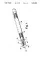
- FIG. 1is a perspective view illustrating an encapsulated transponder apparatus illustrating one application of the present invention
- FIG. 2is a perspective view more clearly illustrating a preferred embodiment of the present invention
- FIG. 3is a transverse cross-section taken in the plane 3--3 of FIG. 2.
- FIG. 1 of the drawingthere is shown a small implantable microtransponder device of the type generally described in the above-mentioned copending application but incorporating the present invention.
- the illustrated deviceincludes an electromagnetic antenna formed of an elongated cylindrical magnetic core 10 having a length of ultra-fine conductive wire 12 wrapped thereabout with the ends 14 and 16 extending forwardly.
- an electromagnetic antennaformed of an elongated cylindrical magnetic core 10 having a length of ultra-fine conductive wire 12 wrapped thereabout with the ends 14 and 16 extending forwardly.
- One such antennais disclosed in copending U.S. patent application Ser. No. 400,600, filed Aug. 30, 1989, and assigned to the assignee of the present invention.
- Affixed to the end of core 10is a support means 18 to which is attached an integrated circuit die 20 having a pair of contact pads 22 and 24 provided thereon in accordance with the present invention.
- the wire end 14is conductively bonded to pad 22, and the wire end 16 is conductively bonded to pad 24.
- the only post-fab testing that need be undertakenis that relating to the bonding of wires 14 and 16 to the pads 22 and 24 respectively, and this can be easily accomplished using automated test equipment. In other words, the usual testing of chip-to-leadframe connection has been eliminated.
- the transponder assemblyis encapsulated in a suitable glass or plastic capsule 26 and is at this point ready for implantation in an animal or other object to be identified.
- the die 20includes electronic memory and associated modulation circuitry such that in response to power input thereto from the coil 12 generates an identifying signal which is returned to coil 12 for retransmission to a detecting antenna.
- the die 20is shown in enlarged detail to include a semiconductive substrate 30 having a standard phosphorus-doped glass layer 32 deposited thereon which is overcovered by a second layer of silicon nitride insulation 34 applied by plasma-enhanced deposition.
- the thickness of layer 34is at least 15,000 angstroms and provides both insulation and structural protection for the underlying die.
- the layer 34is masked and two contact areas or holes 50 are etched through the layers 32 and 34 to contact the ac+ and ac- pads (not shown) on the circuit contained in die 20 beneath layer 32. With the contact areas open, the wafer is ready for the fabrication of the enhanced contact pads 22 and 24.
- the processstarts with the deposition of a field metal layer 36 of TiW (approximately 90% Ti and 10% W) having a thickness of approximately 2,000 angstroms. On top of this layer a layer of pure gold of approximately 1,200 angstroms is deposited.
- TiWapproximately 90% Ti and 10% W
- the enhanced contact pads 22 and 24are then deposited to a thickness of approximately 25 microns of gold or copper.
- the pads 22 and 24are approximately 16 milli-inches long and 6 milli-inches wide and provide adequate surface area to which the fine copper wires 14 and 16 may be attached by soldering, thermal compression bonding or welding.
- the thick silicon nitride il layer 34is of particular importance to the invention in that the pads 22 and 24 are plated directly over the active circuit area, i.e. the layer 34 serves to protect against damage to the underlying circuitry during the wire lead attachment process which would otherwise render the assembly useless.
- FIG. 3 of the drawingwhich is a partially broken cross-section taken along the plane 3--3 of FIG. 2, the manufacturing process is further illustrated, it being understood of course that the illustrated die is not fabricated individually but is made jointly with other die, forming a silicon wafer.
- the die 20is separated from the other die of the wafer.
- the wafer 40 from which the die 20 is cutforms a substrate the upper portion 42 of which has integrated circuit components formed therein.
- Deposited on the usual upper surface of the wafer and forming a standard electrical interconnect pad 44is a metallization layer 46.
- a supporting leadframeis normally electronically connected to pads 44 by fine wires.
- a second layer 52 of photoresist of about 30 microns thicknessis deposited over the wafer, and openings 54 are formed therein to define the enhanced pads 22 and 24 and reopen the holes 50.
- the field metal layers 36 and 38are then deposited, typically using a DC-diode sputtering process, and subsequently the 25-micron thick enhanced pads 22 (FIG. 2) and 24 are electroplated onto the field metal.
- the photoresistis then removed, and the dies are severed from the wafer to yield the structure illustrated in FIG. 2. It will be understood of course that testing can be accomplished either before the dies are separated or afterwards.
- the diemay be bonded to a support plate 18, as depicted in FIGS. 1 and 2, and the leads 14 and 16 are attached to the enhanced pads 22 and 24 respectively, by soldering, thermal compression bonding or welding.
- the wire attachment operationis made directly to a component part of the die, i.e. the enhanced pads 22 and 24 rather than to leadframes, as described in the previously mentioned copending application, the underlying circuit is protected by a combination of the layer 34 and the structural characteristics of the pads 22 and 24.
Landscapes
- Engineering & Computer Science (AREA)
- Physics & Mathematics (AREA)
- General Physics & Mathematics (AREA)
- Radar, Positioning & Navigation (AREA)
- Remote Sensing (AREA)
- Microelectronics & Electronic Packaging (AREA)
- Computer Hardware Design (AREA)
- Theoretical Computer Science (AREA)
- Life Sciences & Earth Sciences (AREA)
- General Life Sciences & Earth Sciences (AREA)
- Geophysics (AREA)
- Computer Networks & Wireless Communication (AREA)
- Power Engineering (AREA)
- Wire Bonding (AREA)
Abstract
Description
Claims (12)
Priority Applications (9)
| Application Number | Priority Date | Filing Date | Title |
|---|---|---|---|
| US07/710,786US5281855A (en) | 1991-06-05 | 1991-06-05 | Integrated circuit device including means for facilitating connection of antenna lead wires to an integrated circuit die |
| US07/787,828US5223851A (en) | 1991-06-05 | 1991-11-05 | Apparatus for facilitating interconnection of antenna lead wires to an integrated circuit and encapsulating the assembly to form an improved miniature transponder device |
| JP5500941AJP2782558B2 (en) | 1991-06-05 | 1992-06-05 | Improved small transponder |
| PCT/US1992/004731WO1992022827A1 (en) | 1991-06-05 | 1992-06-05 | An improved miniature transponder device |
| DE69222526TDE69222526T2 (en) | 1991-06-05 | 1992-06-05 | IMPROVED MINIATURE TRANSPONDER |
| EP92913812AEP0588944B1 (en) | 1991-06-05 | 1992-06-05 | An improved miniature transponder device |
| DE0588944TDE588944T1 (en) | 1991-06-05 | 1992-06-05 | IMPROVED MINIATURE TRANSPONDER. |
| AU21902/92AAU2190292A (en) | 1991-06-05 | 1992-06-05 | An improved miniature transponder device |
| DE9218940UDE9218940U1 (en) | 1991-06-05 | 1992-06-05 | Miniature transponder |
Applications Claiming Priority (1)
| Application Number | Priority Date | Filing Date | Title |
|---|---|---|---|
| US07/710,786US5281855A (en) | 1991-06-05 | 1991-06-05 | Integrated circuit device including means for facilitating connection of antenna lead wires to an integrated circuit die |
Related Child Applications (1)
| Application Number | Title | Priority Date | Filing Date |
|---|---|---|---|
| US07/787,828Continuation-In-PartUS5223851A (en) | 1991-06-05 | 1991-11-05 | Apparatus for facilitating interconnection of antenna lead wires to an integrated circuit and encapsulating the assembly to form an improved miniature transponder device |
Publications (1)
| Publication Number | Publication Date |
|---|---|
| US5281855Atrue US5281855A (en) | 1994-01-25 |
Family
ID=24855530
Family Applications (1)
| Application Number | Title | Priority Date | Filing Date |
|---|---|---|---|
| US07/710,786Expired - LifetimeUS5281855A (en) | 1991-06-05 | 1991-06-05 | Integrated circuit device including means for facilitating connection of antenna lead wires to an integrated circuit die |
Country Status (1)
| Country | Link |
|---|---|
| US (1) | US5281855A (en) |
Cited By (69)
| Publication number | Priority date | Publication date | Assignee | Title |
|---|---|---|---|---|
| US5506499A (en)* | 1995-06-05 | 1996-04-09 | Neomagic Corp. | Multiple probing of an auxilary test pad which allows for reliable bonding to a primary bonding pad |
| DE19509999A1 (en)* | 1995-03-22 | 1996-09-26 | David Finn | Method and device for producing a transponder unit and transponder unit |
| US5572410A (en)* | 1991-02-25 | 1996-11-05 | Gustafson; Ake | Integrated circuit device having a winding connected to an integrated circuit solely by a wire |
| US5606488A (en)* | 1990-04-19 | 1997-02-25 | Sokymat Sa | Miniaturized printed circuit and coil assembly |
| US5621199A (en)* | 1995-04-03 | 1997-04-15 | Datalogic, Inc. | RFID reader |
| US5963132A (en)* | 1996-10-11 | 1999-10-05 | Avid Indentification Systems, Inc. | Encapsulated implantable transponder |
| US6017496A (en) | 1995-06-07 | 2000-01-25 | Irori | Matrices with memories and uses thereof |
| US6078259A (en)* | 1994-09-09 | 2000-06-20 | Intermec Ip Corp. | Radio frequency identification tag |
| US6088230A (en)* | 1994-03-28 | 2000-07-11 | Finn; David | Procedure for producing a chip mounting board and chip-mounting board thus produced |
| EP0997843A3 (en)* | 1998-10-29 | 2000-11-02 | AEG Identifikationssysteme GmbH | Transponder arrangement and method for the production of a transponder arrangement |
| US6211786B1 (en) | 1999-04-30 | 2001-04-03 | Holtek Semiconductor Inc. | Battery-free circuit device for RF identifying tag |
| US6275153B1 (en) | 2000-07-26 | 2001-08-14 | Andrew Brooks | Identification and tracking system |
| US6329139B1 (en) | 1995-04-25 | 2001-12-11 | Discovery Partners International | Automated sorting system for matrices with memory |
| US6400338B1 (en) | 2000-01-11 | 2002-06-04 | Destron-Fearing Corporation | Passive integrated transponder tag with unitary antenna core |
| US6441741B1 (en) | 1999-05-17 | 2002-08-27 | Avid Identification Systems, Inc. | Overmolded transponder |
| US20030018364A1 (en)* | 2001-07-17 | 2003-01-23 | Medtronic, Inc. | Enhanced method and apparatus to identify and connect a small diameter lead with a low profile lead connector |
| US20030172968A1 (en)* | 2001-05-15 | 2003-09-18 | Pharma Seq, Inc. | Method and apparatus for powering circuitry with on-chip solar cells within a common substrate |
| US6675049B2 (en) | 2001-07-17 | 2004-01-06 | Medtronic, Inc. | Method and apparatus for automatic implantable medical lead recognition and configuration |
| WO2004042818A1 (en)* | 2002-11-08 | 2004-05-21 | Koninklijke Philips Electronics N.V. | Integrated circuit with at least one bump |
| US6856250B2 (en) | 2002-01-11 | 2005-02-15 | Randy Hilliard | Tracking system, apparatus and method |
| US20060267774A1 (en)* | 2005-03-24 | 2006-11-30 | Feinberg Stewart C | Transponder overmolded with ethylene copolymers |
| EP1816592A1 (en) | 2006-02-06 | 2007-08-08 | Assa Abloy Identification Technology Group AB | Method for producing a RFID tag with at least an antenna comprising two extremities and a integrated circuit chip |
| US20080073800A1 (en)* | 2006-09-26 | 2008-03-27 | Advanced Microelectronic And Automation Technology Ltd. | Methods of connecting an antenna to a transponder chip |
| US20080072423A1 (en)* | 2006-09-26 | 2008-03-27 | Advanced Microelectronic And Automation Technology Ltd. | Secure high frequency / ultra high frequency inlay, and method and apparatus for making the inlay |
| WO2008037592A1 (en) | 2006-09-26 | 2008-04-03 | Advanced Micromechanic And Automation Technology Ltd | Method of connecting an antenna to a transponder chip and corresponding transponder inlay |
| WO2008065127A2 (en) | 2006-11-30 | 2008-06-05 | Lutronic International S.A. | Miniature transponder and identification system including said transponder and a suitable reader |
| US20080150817A1 (en)* | 2006-09-26 | 2008-06-26 | Lionel Carre | Method and Apparatus for Making A Radio Frequency Inlay |
| US20080179404A1 (en)* | 2006-09-26 | 2008-07-31 | Advanced Microelectronic And Automation Technology Ltd. | Methods and apparatuses to produce inlays with transponders |
| WO2008107274A1 (en)* | 2007-02-21 | 2008-09-12 | Em Microelectronic-Marin Sa | Process for manufacturing a device comprising an integrated circuit and an antenna coil connected to it |
| US20080283615A1 (en)* | 2007-05-17 | 2008-11-20 | Advanced Microelectronic And Automation Technology Ltd. | Dual interface inlays |
| US20080308641A1 (en)* | 2007-04-10 | 2008-12-18 | Advanced Microelectronic And Automation Technology Ltd. | Smart card with switchable matching antenna |
| US20090009418A1 (en)* | 2007-07-03 | 2009-01-08 | Masin Joseph V | Miniature transponders |
| US20090033585A1 (en)* | 2004-11-02 | 2009-02-05 | Imasys Ag | Laying apparatus, contact-making apparatus, movement system, laying and contact-making unit, production system, method for production and a transponder unit |
| US20090100667A1 (en)* | 2007-09-18 | 2009-04-23 | Aontec Teoranta | Method for bonding a wire conductor laid on a substrate |
| US20090213027A1 (en)* | 2007-04-10 | 2009-08-27 | Advanced Microelectronic And Automation Technology Ltd. | Methods of connecting an antenna to a transponder chip |
| US7581308B2 (en) | 2007-01-01 | 2009-09-01 | Advanced Microelectronic And Automation Technology Ltd. | Methods of connecting an antenna to a transponder chip |
| US20090315320A1 (en)* | 2006-09-26 | 2009-12-24 | Advanced Microelectronic And Automation Technology Ltd. | Inlays for security documents |
| EP2175400A1 (en) | 2008-10-08 | 2010-04-14 | NagralD | Method of manufacturing an RF communication device made up of an antenna cable connected to an electronic unit |
| US20100141453A1 (en)* | 2006-09-26 | 2010-06-10 | Assa Abloy Identification Technology Group Ab | Method and Apparatus for Making a Radio Frequency Inlay |
| CN101170210B (en)* | 2006-10-24 | 2011-08-10 | 珠海利安科技有限公司 | Novel waterproof digital TV antenna with amplification function |
| WO2012103203A3 (en)* | 2011-01-27 | 2012-11-01 | Texas Instruments Incorporated | Frid transponder and method for connecting semiconductor die to antenna |
| US20140079405A1 (en)* | 2011-04-21 | 2014-03-20 | The Flewelling Ford Family Trust | Overmoulding method and overmoulded electronic device |
| US8789762B2 (en) | 2010-08-12 | 2014-07-29 | Feinics Amatech Teoranta | RFID antenna modules and methods of making |
| US8823244B2 (en) | 2008-11-20 | 2014-09-02 | Ceramtec Gmbh | Monolithic multi-layered actuator with external electrodes made of a metallic, porous, expandable conductive layer |
| US8991712B2 (en) | 2010-08-12 | 2015-03-31 | Féinics Amatech Teoranta | Coupling in and to RFID smart cards |
| US9256773B2 (en) | 2011-07-27 | 2016-02-09 | Féinics Amatech Teoranta | Capacitive coupling of an RFID tag with a touch screen device acting as a reader |
| US9475086B2 (en) | 2013-01-18 | 2016-10-25 | Féinics Amatech Teoranta | Smartcard with coupling frame and method of increasing activation distance of a transponder chip module |
| US9489613B2 (en) | 2011-08-08 | 2016-11-08 | Féinics Amatech Teoranta | RFID transponder chip modules with a band of the antenna extending inward |
| US9622359B2 (en) | 2011-08-08 | 2017-04-11 | Féinics Amatech Teoranta | RFID transponder chip modules |
| US9634391B2 (en) | 2011-08-08 | 2017-04-25 | Féinics Amatech Teoranta | RFID transponder chip modules |
| US9697459B2 (en) | 2014-08-10 | 2017-07-04 | Féinics Amatech Teoranta | Passive smart cards, metal cards, payment objects and smart jewelry |
| US9798968B2 (en) | 2013-01-18 | 2017-10-24 | Féinics Amatech Teoranta | Smartcard with coupling frame and method of increasing activation distance of a transponder chip module |
| US9812782B2 (en) | 2011-08-08 | 2017-11-07 | Féinics Amatech Teoranta | Coupling frames for RFID devices |
| CN107318739A (en)* | 2017-07-04 | 2017-11-07 | 浙江海洋大学 | A kind of abyssal fishes metal magnetic line mark |
| US9836684B2 (en) | 2014-08-10 | 2017-12-05 | Féinics Amatech Teoranta | Smart cards, payment objects and methods |
| US20180062436A1 (en)* | 2016-08-26 | 2018-03-01 | Nucurrent, Inc. | Wireless Connector Transmitter Module With an Electrical Connector |
| US10248902B1 (en) | 2017-11-06 | 2019-04-02 | Féinics Amatech Teoranta | Coupling frames for RFID devices |
| US10518518B2 (en) | 2013-01-18 | 2019-12-31 | Féinics Amatech Teoranta | Smart cards with metal layer(s) and methods of manufacture |
| US10552722B2 (en) | 2014-08-10 | 2020-02-04 | Féinics Amatech Teoranta | Smartcard with coupling frame antenna |
| US10599972B2 (en) | 2013-01-18 | 2020-03-24 | Féinics Amatech Teoranta | Smartcard constructions and methods |
| US10733494B2 (en) | 2014-08-10 | 2020-08-04 | Féinics Amatech Teoranta | Contactless metal card constructions |
| US10824931B2 (en) | 2012-08-30 | 2020-11-03 | Féinics Amatech Teoranta | Contactless smartcards with multiple coupling frames |
| US10977542B2 (en) | 2013-01-18 | 2021-04-13 | Amtech Group Limited Industrial Estate | Smart cards with metal layer(s) and methods of manufacture |
| USD942538S1 (en) | 2020-07-30 | 2022-02-01 | Federal Card Services, LLC | Asymmetrical arrangement of contact pads and connection bridges of a transponder chip module |
| USD943024S1 (en) | 2020-07-30 | 2022-02-08 | Federal Card Services, LLC | Asymmetrical arrangement of contact pads and connection bridges of a transponder chip module |
| US11354560B2 (en) | 2013-01-18 | 2022-06-07 | Amatech Group Limited | Smartcards with multiple coupling frames |
| US11354558B2 (en) | 2013-01-18 | 2022-06-07 | Amatech Group Limited | Contactless smartcards with coupling frames |
| US11361204B2 (en) | 2018-03-07 | 2022-06-14 | X-Card Holdings, Llc | Metal card |
| US11551051B2 (en) | 2013-01-18 | 2023-01-10 | Amatech Group Limiied | Coupling frames for smartcards with various module opening shapes |
Citations (15)
| Publication number | Priority date | Publication date | Assignee | Title |
|---|---|---|---|---|
| US3609741A (en)* | 1969-03-21 | 1971-09-28 | Wendell S Miller | Prevention of unauthorized movement of articles between predetermined areas |
| US4001822A (en)* | 1974-05-28 | 1977-01-04 | Rca Corporation | Electronic license plate for motor vehicles |
| US4017886A (en)* | 1972-10-18 | 1977-04-12 | Hitachi, Ltd. | Discrete semiconductor device having polymer resin as insulator and method for making the same |
| US4273859A (en)* | 1979-12-31 | 1981-06-16 | Honeywell Information Systems Inc. | Method of forming solder bump terminals on semiconductor elements |
| US4507852A (en)* | 1983-09-12 | 1985-04-02 | Rockwell International Corporation | Method for making a reliable ohmic contact between two layers of integrated circuit metallizations |
| WO1987004900A1 (en)* | 1986-02-25 | 1987-08-27 | Identification Devices, Inc. | Syringe-implantable identification transponder |
| US4805232A (en)* | 1987-01-15 | 1989-02-14 | Ma John Y | Ferrite-core antenna |
| US4857893A (en)* | 1986-07-18 | 1989-08-15 | Bi Inc. | Single chip transponder device |
| US4984061A (en)* | 1987-05-15 | 1991-01-08 | Kabushiki Kaisha Toshiba | Semiconductor device in which wiring layer is formed below bonding pad |
| US4990993A (en)* | 1980-04-25 | 1991-02-05 | Hitachi, Ltd. | Resin-molded semiconductor device using polymide and nitride films for the passivation film |
| US4992794A (en)* | 1988-10-10 | 1991-02-12 | Texas Instruments Incorporated | Transponder and method for the production thereof |
| US5025550A (en)* | 1990-05-25 | 1991-06-25 | Trovan Limited | Automated method for the manufacture of small implantable transponder devices |
| US5050292A (en)* | 1990-05-25 | 1991-09-24 | Trovan Limited | Automated method for the manufacture of transponder devices by winding around a bobbin |
| US5136271A (en)* | 1989-01-09 | 1992-08-04 | Mitsubishi Denki Kabushiki Kaisha | Microwave integrated circuit mountings |
| US5142698A (en)* | 1988-06-08 | 1992-08-25 | Nec Corporation | Microwave integrated apparatus including antenna pattern for satellite broadcasting receiver |
- 1991
- 1991-06-05USUS07/710,786patent/US5281855A/ennot_activeExpired - Lifetime
Patent Citations (15)
| Publication number | Priority date | Publication date | Assignee | Title |
|---|---|---|---|---|
| US3609741A (en)* | 1969-03-21 | 1971-09-28 | Wendell S Miller | Prevention of unauthorized movement of articles between predetermined areas |
| US4017886A (en)* | 1972-10-18 | 1977-04-12 | Hitachi, Ltd. | Discrete semiconductor device having polymer resin as insulator and method for making the same |
| US4001822A (en)* | 1974-05-28 | 1977-01-04 | Rca Corporation | Electronic license plate for motor vehicles |
| US4273859A (en)* | 1979-12-31 | 1981-06-16 | Honeywell Information Systems Inc. | Method of forming solder bump terminals on semiconductor elements |
| US4990993A (en)* | 1980-04-25 | 1991-02-05 | Hitachi, Ltd. | Resin-molded semiconductor device using polymide and nitride films for the passivation film |
| US4507852A (en)* | 1983-09-12 | 1985-04-02 | Rockwell International Corporation | Method for making a reliable ohmic contact between two layers of integrated circuit metallizations |
| WO1987004900A1 (en)* | 1986-02-25 | 1987-08-27 | Identification Devices, Inc. | Syringe-implantable identification transponder |
| US4857893A (en)* | 1986-07-18 | 1989-08-15 | Bi Inc. | Single chip transponder device |
| US4805232A (en)* | 1987-01-15 | 1989-02-14 | Ma John Y | Ferrite-core antenna |
| US4984061A (en)* | 1987-05-15 | 1991-01-08 | Kabushiki Kaisha Toshiba | Semiconductor device in which wiring layer is formed below bonding pad |
| US5142698A (en)* | 1988-06-08 | 1992-08-25 | Nec Corporation | Microwave integrated apparatus including antenna pattern for satellite broadcasting receiver |
| US4992794A (en)* | 1988-10-10 | 1991-02-12 | Texas Instruments Incorporated | Transponder and method for the production thereof |
| US5136271A (en)* | 1989-01-09 | 1992-08-04 | Mitsubishi Denki Kabushiki Kaisha | Microwave integrated circuit mountings |
| US5025550A (en)* | 1990-05-25 | 1991-06-25 | Trovan Limited | Automated method for the manufacture of small implantable transponder devices |
| US5050292A (en)* | 1990-05-25 | 1991-09-24 | Trovan Limited | Automated method for the manufacture of transponder devices by winding around a bobbin |
Cited By (116)
| Publication number | Priority date | Publication date | Assignee | Title |
|---|---|---|---|---|
| US5606488A (en)* | 1990-04-19 | 1997-02-25 | Sokymat Sa | Miniaturized printed circuit and coil assembly |
| US5649352A (en)* | 1990-04-19 | 1997-07-22 | Sokymat S.A. | Process for assembling a coil on a printed circuit |
| US5790387A (en)* | 1991-02-25 | 1998-08-04 | Gustafson; Ake | Process for fixing a winding to an electronic circuit and a packaged electronic component produced therefrom |
| US20020189080A1 (en)* | 1991-02-25 | 2002-12-19 | Ake Gustafson | Method for fixing a winding to an electronic circuit |
| US5572410A (en)* | 1991-02-25 | 1996-11-05 | Gustafson; Ake | Integrated circuit device having a winding connected to an integrated circuit solely by a wire |
| US5634261A (en)* | 1991-02-25 | 1997-06-03 | Gustafson; Ake | Process for fixing a winding to an electronic circuit |
| US6088230A (en)* | 1994-03-28 | 2000-07-11 | Finn; David | Procedure for producing a chip mounting board and chip-mounting board thus produced |
| US6078259A (en)* | 1994-09-09 | 2000-06-20 | Intermec Ip Corp. | Radio frequency identification tag |
| DE19509999A1 (en)* | 1995-03-22 | 1996-09-26 | David Finn | Method and device for producing a transponder unit and transponder unit |
| US6067235A (en)* | 1995-03-22 | 2000-05-23 | Finn; David | Process and a device for the production of a transponder unit and a transponder unit |
| DE19509999C2 (en)* | 1995-03-22 | 1998-04-16 | David Finn | Method and device for producing a transponder unit and transponder unit |
| US5621199A (en)* | 1995-04-03 | 1997-04-15 | Datalogic, Inc. | RFID reader |
| US6329139B1 (en) | 1995-04-25 | 2001-12-11 | Discovery Partners International | Automated sorting system for matrices with memory |
| US5506499A (en)* | 1995-06-05 | 1996-04-09 | Neomagic Corp. | Multiple probing of an auxilary test pad which allows for reliable bonding to a primary bonding pad |
| US6017496A (en) | 1995-06-07 | 2000-01-25 | Irori | Matrices with memories and uses thereof |
| US5963132A (en)* | 1996-10-11 | 1999-10-05 | Avid Indentification Systems, Inc. | Encapsulated implantable transponder |
| EP0997843A3 (en)* | 1998-10-29 | 2000-11-02 | AEG Identifikationssysteme GmbH | Transponder arrangement and method for the production of a transponder arrangement |
| US6211786B1 (en) | 1999-04-30 | 2001-04-03 | Holtek Semiconductor Inc. | Battery-free circuit device for RF identifying tag |
| US6778089B2 (en) | 1999-05-17 | 2004-08-17 | Avid Identification Systems, Inc. | Overmolded transponder |
| US6441741B1 (en) | 1999-05-17 | 2002-08-27 | Avid Identification Systems, Inc. | Overmolded transponder |
| US7109868B2 (en) | 1999-05-17 | 2006-09-19 | Avid Identification Systems, Inc. | Unitary core transponder |
| US20050012620A1 (en)* | 1999-05-17 | 2005-01-20 | Jay Yoakum | Unitary core transponder |
| US6400338B1 (en) | 2000-01-11 | 2002-06-04 | Destron-Fearing Corporation | Passive integrated transponder tag with unitary antenna core |
| AU759268B2 (en)* | 2000-01-11 | 2003-04-10 | Digital Angel Corporation | Passive integrated transponder tag with unitary antenna core |
| US6275153B1 (en) | 2000-07-26 | 2001-08-14 | Andrew Brooks | Identification and tracking system |
| US20030172968A1 (en)* | 2001-05-15 | 2003-09-18 | Pharma Seq, Inc. | Method and apparatus for powering circuitry with on-chip solar cells within a common substrate |
| US7098394B2 (en) | 2001-05-15 | 2006-08-29 | Pharmaseq, Inc. | Method and apparatus for powering circuitry with on-chip solar cells within a common substrate |
| US20040078067A1 (en)* | 2001-07-17 | 2004-04-22 | Medtronic, Inc. | Method and apparatus for automatic implantable medical lead recognition and configuration |
| US6968235B2 (en) | 2001-07-17 | 2005-11-22 | Medtronic, Inc. | Enhanced method and apparatus to identify and connect a small diameter lead with a low profile lead connector |
| US20030018364A1 (en)* | 2001-07-17 | 2003-01-23 | Medtronic, Inc. | Enhanced method and apparatus to identify and connect a small diameter lead with a low profile lead connector |
| US6675049B2 (en) | 2001-07-17 | 2004-01-06 | Medtronic, Inc. | Method and apparatus for automatic implantable medical lead recognition and configuration |
| US20040176822A1 (en)* | 2001-07-17 | 2004-09-09 | Medtronic, Inc. | Method and apparatus for automatic implantable medical lead recognition and configuration |
| US7239916B2 (en) | 2001-07-17 | 2007-07-03 | Medtronic, Inc. | Method and apparatus for automatic implantable medical lead recognition and configuration |
| US6856250B2 (en) | 2002-01-11 | 2005-02-15 | Randy Hilliard | Tracking system, apparatus and method |
| CN100382293C (en)* | 2002-11-08 | 2008-04-16 | Nxp股份有限公司 | Integrated circuit with at least one bump |
| WO2004042818A1 (en)* | 2002-11-08 | 2004-05-21 | Koninklijke Philips Electronics N.V. | Integrated circuit with at least one bump |
| US20090033585A1 (en)* | 2004-11-02 | 2009-02-05 | Imasys Ag | Laying apparatus, contact-making apparatus, movement system, laying and contact-making unit, production system, method for production and a transponder unit |
| US8646675B2 (en) | 2004-11-02 | 2014-02-11 | Hid Global Gmbh | Laying apparatus, contact-making apparatus, movement system, laying and contact-making unit, production system, method for production and a transponder unit |
| US20060267774A1 (en)* | 2005-03-24 | 2006-11-30 | Feinberg Stewart C | Transponder overmolded with ethylene copolymers |
| EP1816592A1 (en) | 2006-02-06 | 2007-08-08 | Assa Abloy Identification Technology Group AB | Method for producing a RFID tag with at least an antenna comprising two extremities and a integrated circuit chip |
| US20080179404A1 (en)* | 2006-09-26 | 2008-07-31 | Advanced Microelectronic And Automation Technology Ltd. | Methods and apparatuses to produce inlays with transponders |
| US8091208B2 (en) | 2006-09-26 | 2012-01-10 | David Finn | Method of forming an inlay substrate having an antenna wire |
| US8608080B2 (en) | 2006-09-26 | 2013-12-17 | Feinics Amatech Teoranta | Inlays for security documents |
| US20080150817A1 (en)* | 2006-09-26 | 2008-06-26 | Lionel Carre | Method and Apparatus for Making A Radio Frequency Inlay |
| US8286332B2 (en) | 2006-09-26 | 2012-10-16 | Hid Global Gmbh | Method and apparatus for making a radio frequency inlay |
| WO2008037592A1 (en) | 2006-09-26 | 2008-04-03 | Advanced Micromechanic And Automation Technology Ltd | Method of connecting an antenna to a transponder chip and corresponding transponder inlay |
| US8240022B2 (en) | 2006-09-26 | 2012-08-14 | Feinics Amatech Teorowita | Methods of connecting an antenna to a transponder chip |
| US20080073800A1 (en)* | 2006-09-26 | 2008-03-27 | Advanced Microelectronic And Automation Technology Ltd. | Methods of connecting an antenna to a transponder chip |
| US7546671B2 (en) | 2006-09-26 | 2009-06-16 | Micromechanic And Automation Technology Ltd. | Method of forming an inlay substrate having an antenna wire |
| US7971339B2 (en) | 2006-09-26 | 2011-07-05 | Hid Global Gmbh | Method and apparatus for making a radio frequency inlay |
| US20100141453A1 (en)* | 2006-09-26 | 2010-06-10 | Assa Abloy Identification Technology Group Ab | Method and Apparatus for Making a Radio Frequency Inlay |
| US20080072423A1 (en)* | 2006-09-26 | 2008-03-27 | Advanced Microelectronic And Automation Technology Ltd. | Secure high frequency / ultra high frequency inlay, and method and apparatus for making the inlay |
| US20090315320A1 (en)* | 2006-09-26 | 2009-12-24 | Advanced Microelectronic And Automation Technology Ltd. | Inlays for security documents |
| CN101170210B (en)* | 2006-10-24 | 2011-08-10 | 珠海利安科技有限公司 | Novel waterproof digital TV antenna with amplification function |
| US20100084464A1 (en)* | 2006-11-30 | 2010-04-08 | Lutronic International S.A. | Miniature Transponder and Identification System Including Said Transponder and a Suitable Reader |
| WO2008065127A3 (en)* | 2006-11-30 | 2008-07-24 | Lutronic Internat S A | Miniature transponder and identification system including said transponder and a suitable reader |
| WO2008065127A2 (en) | 2006-11-30 | 2008-06-05 | Lutronic International S.A. | Miniature transponder and identification system including said transponder and a suitable reader |
| FR2909258A1 (en)* | 2006-11-30 | 2008-06-06 | Prosonic Soc Par Actions Simpl | MINIATURE TRANSPONDER AND IDENTIFICATION SYSTEM COMPRISING SUCH A TRANSPONDER AND AN ADAPTIVE READER. |
| US7581308B2 (en) | 2007-01-01 | 2009-09-01 | Advanced Microelectronic And Automation Technology Ltd. | Methods of connecting an antenna to a transponder chip |
| WO2008107230A1 (en)* | 2007-02-21 | 2008-09-12 | Em Microelectronic-Marin Sa | Process for manufacturing an rfid-type communication device |
| WO2008107274A1 (en)* | 2007-02-21 | 2008-09-12 | Em Microelectronic-Marin Sa | Process for manufacturing a device comprising an integrated circuit and an antenna coil connected to it |
| US20090213027A1 (en)* | 2007-04-10 | 2009-08-27 | Advanced Microelectronic And Automation Technology Ltd. | Methods of connecting an antenna to a transponder chip |
| US8322624B2 (en) | 2007-04-10 | 2012-12-04 | Feinics Amatech Teoranta | Smart card with switchable matching antenna |
| US20080308641A1 (en)* | 2007-04-10 | 2008-12-18 | Advanced Microelectronic And Automation Technology Ltd. | Smart card with switchable matching antenna |
| US7979975B2 (en) | 2007-04-10 | 2011-07-19 | Feinics Amatech Teavanta | Methods of connecting an antenna to a transponder chip |
| US7980477B2 (en) | 2007-05-17 | 2011-07-19 | Féinics Amatech Teoranta | Dual interface inlays |
| US20080283615A1 (en)* | 2007-05-17 | 2008-11-20 | Advanced Microelectronic And Automation Technology Ltd. | Dual interface inlays |
| US7825869B2 (en) | 2007-07-03 | 2010-11-02 | Masin Joseph V | Miniature transponders |
| US20090009418A1 (en)* | 2007-07-03 | 2009-01-08 | Masin Joseph V | Miniature transponders |
| US8413316B2 (en) | 2007-09-18 | 2013-04-09 | Hid Global Ireland Teoranta | Method for bonding a wire conductor laid on a substrate |
| US20090100667A1 (en)* | 2007-09-18 | 2009-04-23 | Aontec Teoranta | Method for bonding a wire conductor laid on a substrate |
| EP2175400A1 (en) | 2008-10-08 | 2010-04-14 | NagralD | Method of manufacturing an RF communication device made up of an antenna cable connected to an electronic unit |
| US8823244B2 (en) | 2008-11-20 | 2014-09-02 | Ceramtec Gmbh | Monolithic multi-layered actuator with external electrodes made of a metallic, porous, expandable conductive layer |
| US8991712B2 (en) | 2010-08-12 | 2015-03-31 | Féinics Amatech Teoranta | Coupling in and to RFID smart cards |
| US8789762B2 (en) | 2010-08-12 | 2014-07-29 | Feinics Amatech Teoranta | RFID antenna modules and methods of making |
| WO2012103203A3 (en)* | 2011-01-27 | 2012-11-01 | Texas Instruments Incorporated | Frid transponder and method for connecting semiconductor die to antenna |
| US20140079405A1 (en)* | 2011-04-21 | 2014-03-20 | The Flewelling Ford Family Trust | Overmoulding method and overmoulded electronic device |
| US9256773B2 (en) | 2011-07-27 | 2016-02-09 | Féinics Amatech Teoranta | Capacitive coupling of an RFID tag with a touch screen device acting as a reader |
| US9812782B2 (en) | 2011-08-08 | 2017-11-07 | Féinics Amatech Teoranta | Coupling frames for RFID devices |
| US9489613B2 (en) | 2011-08-08 | 2016-11-08 | Féinics Amatech Teoranta | RFID transponder chip modules with a band of the antenna extending inward |
| US9622359B2 (en) | 2011-08-08 | 2017-04-11 | Féinics Amatech Teoranta | RFID transponder chip modules |
| US9634391B2 (en) | 2011-08-08 | 2017-04-25 | Féinics Amatech Teoranta | RFID transponder chip modules |
| US10824931B2 (en) | 2012-08-30 | 2020-11-03 | Féinics Amatech Teoranta | Contactless smartcards with multiple coupling frames |
| US11568195B2 (en) | 2013-01-18 | 2023-01-31 | Amatech Group Limited | Smart cards with metal layer(s) and methods of manufacture |
| US9798968B2 (en) | 2013-01-18 | 2017-10-24 | Féinics Amatech Teoranta | Smartcard with coupling frame and method of increasing activation distance of a transponder chip module |
| US11836565B2 (en) | 2013-01-18 | 2023-12-05 | Amatech Group Limited | Smartcards with multiple coupling frames |
| US10977542B2 (en) | 2013-01-18 | 2021-04-13 | Amtech Group Limited Industrial Estate | Smart cards with metal layer(s) and methods of manufacture |
| US11551051B2 (en) | 2013-01-18 | 2023-01-10 | Amatech Group Limiied | Coupling frames for smartcards with various module opening shapes |
| US11354558B2 (en) | 2013-01-18 | 2022-06-07 | Amatech Group Limited | Contactless smartcards with coupling frames |
| US10518518B2 (en) | 2013-01-18 | 2019-12-31 | Féinics Amatech Teoranta | Smart cards with metal layer(s) and methods of manufacture |
| US11354560B2 (en) | 2013-01-18 | 2022-06-07 | Amatech Group Limited | Smartcards with multiple coupling frames |
| US10599972B2 (en) | 2013-01-18 | 2020-03-24 | Féinics Amatech Teoranta | Smartcard constructions and methods |
| US11037044B2 (en) | 2013-01-18 | 2021-06-15 | Amatech Group Limited | Smartcard constructions and methods |
| US9475086B2 (en) | 2013-01-18 | 2016-10-25 | Féinics Amatech Teoranta | Smartcard with coupling frame and method of increasing activation distance of a transponder chip module |
| US9836684B2 (en) | 2014-08-10 | 2017-12-05 | Féinics Amatech Teoranta | Smart cards, payment objects and methods |
| US10733494B2 (en) | 2014-08-10 | 2020-08-04 | Féinics Amatech Teoranta | Contactless metal card constructions |
| US9697459B2 (en) | 2014-08-10 | 2017-07-04 | Féinics Amatech Teoranta | Passive smart cards, metal cards, payment objects and smart jewelry |
| US10552722B2 (en) | 2014-08-10 | 2020-02-04 | Féinics Amatech Teoranta | Smartcard with coupling frame antenna |
| US20180062436A1 (en)* | 2016-08-26 | 2018-03-01 | Nucurrent, Inc. | Wireless Connector Transmitter Module With an Electrical Connector |
| US10897140B2 (en) | 2016-08-26 | 2021-01-19 | Nucurrent, Inc. | Method of operating a wireless connector system |
| US10931118B2 (en)* | 2016-08-26 | 2021-02-23 | Nucurrent, Inc. | Wireless connector transmitter module with an electrical connector |
| US10938220B2 (en) | 2016-08-26 | 2021-03-02 | Nucurrent, Inc. | Wireless connector system |
| US10879705B2 (en) | 2016-08-26 | 2020-12-29 | Nucurrent, Inc. | Wireless connector receiver module with an electrical connector |
| US11011915B2 (en) | 2016-08-26 | 2021-05-18 | Nucurrent, Inc. | Method of making a wireless connector transmitter module |
| US10903660B2 (en) | 2016-08-26 | 2021-01-26 | Nucurrent, Inc. | Wireless connector system circuit |
| US12327931B2 (en) | 2016-08-26 | 2025-06-10 | Nucurrent, Inc. | Wireless connector system |
| US10886751B2 (en) | 2016-08-26 | 2021-01-05 | Nucurrent, Inc. | Wireless connector transmitter module |
| US10916950B2 (en) | 2016-08-26 | 2021-02-09 | Nucurrent, Inc. | Method of making a wireless connector receiver module |
| US10879704B2 (en) | 2016-08-26 | 2020-12-29 | Nucurrent, Inc. | Wireless connector receiver module |
| CN107318739A (en)* | 2017-07-04 | 2017-11-07 | 浙江海洋大学 | A kind of abyssal fishes metal magnetic line mark |
| US10248902B1 (en) | 2017-11-06 | 2019-04-02 | Féinics Amatech Teoranta | Coupling frames for RFID devices |
| US11361204B2 (en) | 2018-03-07 | 2022-06-14 | X-Card Holdings, Llc | Metal card |
| US11853824B2 (en) | 2018-03-07 | 2023-12-26 | X-Card Holdings, Llc | Metal card |
| US12204966B2 (en) | 2018-03-07 | 2025-01-21 | X-Card Holdings, Llc | Metal card |
| USD943024S1 (en) | 2020-07-30 | 2022-02-08 | Federal Card Services, LLC | Asymmetrical arrangement of contact pads and connection bridges of a transponder chip module |
| USD942538S1 (en) | 2020-07-30 | 2022-02-01 | Federal Card Services, LLC | Asymmetrical arrangement of contact pads and connection bridges of a transponder chip module |
Similar Documents
| Publication | Publication Date | Title |
|---|---|---|
| US5281855A (en) | Integrated circuit device including means for facilitating connection of antenna lead wires to an integrated circuit die | |
| US5223851A (en) | Apparatus for facilitating interconnection of antenna lead wires to an integrated circuit and encapsulating the assembly to form an improved miniature transponder device | |
| US6201186B1 (en) | Electronic component assembly and method of making the same | |
| US6258629B1 (en) | Electronic device package and leadframe and method for making the package | |
| US5677566A (en) | Semiconductor chip package | |
| US5814877A (en) | Single layer leadframe design with groundplane capability | |
| US4891687A (en) | Multi-layer molded plastic IC package | |
| KR860000410B1 (en) | A semiconductor device and a method for fabricating the same | |
| US6630372B2 (en) | Method for routing die interconnections using intermediate connection elements secured to the die face | |
| EP1020903B1 (en) | A semiconductor device using a lead frame and its manufacturing method | |
| US6437449B1 (en) | Making semiconductor devices having stacked dies with biased back surfaces | |
| EP0902472A2 (en) | Combination inductive coil and integrated circuit semiconductor chip in a single lead frame package and method therefor | |
| US20030015780A1 (en) | Bumped chip carrier package using lead frame and method for manufacturing the same | |
| US20020027271A1 (en) | Dual LOC semiconductor assembly employing floating lead finger structure | |
| EP1994551A2 (en) | Methods of making qfn package with power and ground rings | |
| JP2961673B2 (en) | Direct microcircuit decoupling device | |
| KR100299560B1 (en) | High density integrated circuit assembly combining lead frame leads and conductive traces | |
| US10741415B2 (en) | Thermosonically bonded connection for flip chip packages | |
| JPH02184054A (en) | Hybrid resin-encapsulated semiconductor device | |
| KR100461718B1 (en) | Chip scale package and the method of fabricating the same | |
| GB2199988A (en) | Multi-layer molded plastic ic package | |
| USH1267H (en) | Integrated circuit and lead frame assembly | |
| US6784551B2 (en) | Electronic device having a trimming possibility and at least one semiconductor chip and method for producing the electronic device | |
| USRE35385E (en) | Method for fixing an electronic component and its contacts to a support | |
| JPS6032769Y2 (en) | semiconductor element |
Legal Events
| Date | Code | Title | Description |
|---|---|---|---|
| AS | Assignment | Owner name:TROVAN LIMITEED, A CORP. OF CA Free format text:ASSIGNMENT OF ASSIGNORS INTEREST.;ASSIGNORS:HADDEN, LEONARD D.;ZIRBES, GLEN LEO;REEL/FRAME:005735/0019 Effective date:19910531 | |
| STCF | Information on status: patent grant | Free format text:PATENTED CASE | |
| AS | Assignment | Owner name:ALGERNON PROMOTIONS,INC., PANAMA Free format text:ASSIGNMENT OF ASSIGNORS INTEREST;ASSIGNOR:TROVAN LIMITED;REEL/FRAME:008321/0020 Effective date:19960610 | |
| AS | Assignment | Owner name:ALGERNON PROMOTIONS INC., PANAMA Free format text:ASSIGNMENT OF ASSIGNORS INTEREST;ASSIGNOR:TROVAN LIMITED;REEL/FRAME:008366/0248 Effective date:19960610 | |
| FPAY | Fee payment | Year of fee payment:4 | |
| AS | Assignment | Owner name:OPPENHEIMER POMS SMITH (NOW KNOWN AS OPPENHEIMER W Free format text:ASSIGNMENT OF ASSIGNORS INTEREST;ASSIGNORS:ALGERNON PROMOTIONS, INC., A CORP. OF PANAMA;TROVAN, LTD., AN ISLE OF MAN CORP.;ELECTRONIC IDENTIFICATION DEVICES, LTD., A CORP. OF CALIFORNIA;REEL/FRAME:009693/0671 Effective date:19970630 | |
| FEPP | Fee payment procedure | Free format text:PAYOR NUMBER ASSIGNED (ORIGINAL EVENT CODE: ASPN); ENTITY STATUS OF PATENT OWNER: LARGE ENTITY | |
| FPAY | Fee payment | Year of fee payment:8 | |
| CC | Certificate of correction | ||
| FPAY | Fee payment | Year of fee payment:12 | |
| AS | Assignment | Owner name:ASSA ABLOY EAST EUROPE AB, SWEDEN Free format text:ASSIGNMENT OF ASSIGNORS INTEREST;ASSIGNOR:GUSTAFSON, AKE;REEL/FRAME:017006/0271 Effective date:20051115 |