US5281836A - Semiconductor sensor with perpendicular N and P-channel MOSFET's - Google Patents
Semiconductor sensor with perpendicular N and P-channel MOSFET'sDownload PDFInfo
- Publication number
- US5281836A US5281836AUS07/844,616US84461692AUS5281836AUS 5281836 AUS5281836 AUS 5281836AUS 84461692 AUS84461692 AUS 84461692AUS 5281836 AUS5281836 AUS 5281836A
- Authority
- US
- United States
- Prior art keywords
- membrane
- oscillator
- disposed
- sensor
- channel
- Prior art date
- Legal status (The legal status is an assumption and is not a legal conclusion. Google has not performed a legal analysis and makes no representation as to the accuracy of the status listed.)
- Expired - Lifetime
Links
Images


Classifications
- H—ELECTRICITY
- H05—ELECTRIC TECHNIQUES NOT OTHERWISE PROVIDED FOR
- H05B—ELECTRIC HEATING; ELECTRIC LIGHT SOURCES NOT OTHERWISE PROVIDED FOR; CIRCUIT ARRANGEMENTS FOR ELECTRIC LIGHT SOURCES, IN GENERAL
- H05B3/00—Ohmic-resistance heating
- H05B3/40—Heating elements having the shape of rods or tubes
- H05B3/42—Heating elements having the shape of rods or tubes non-flexible
- H05B3/48—Heating elements having the shape of rods or tubes non-flexible heating conductor embedded in insulating material
Definitions
- the inventionrelates to the field of sensors using field effect semiconductor devices. It relates more particularly to a sensor for measuring a physical (i.e. non-electrical) property such as pressure, stress, deformation, temperature, etc. . . . , and constituted in the form of a ring oscillator using metal oxide semiconductor field effect transistors (MOSFETs).
- a physical propertysuch as pressure, stress, deformation, temperature, etc. . . .
- MOSFETsmetal oxide semiconductor field effect transistors
- siliconthe base material from which MOSFETs are made, has piezoresistive properties that are of interest in the field of sensors.
- CMOScomplementary metal oxide semiconductor
- An object of the inventionis thus to provide a semi conductor sensor having very good sensitivity while maintaining a relatively low cost price. Another object is to eliminate sensor drift under the effect of temperature and to improve the yield of the manufacturing process by reducing the number of rejects.
- the sensor of the inventioncomprises a ring oscillator made up from an odd number of CMOS inverters disposed in a zone which is sensitive to the physical property which is to be measured; for each CMOS inverter, the N channel of the NMOS transistor is substantially perpendicular to the P channel of the PMOS transistor. This serves to increase sensor sensitivity by about 15% to 20% compared with a parallel disposition.
- the sensitive zonemay in particular take the form of a deformable membrane; in which case the physical property to be measured is pressure.
- the senorcomprises at least one pair of ring oscillators so as to reduce sensor drift related to temperature variations.
- the sensitive zone of the sensoris provided with a plurality of ring oscillator pairs, thereby reducing the number of rejects during the manufacturing process.
- the senormay also be provided with at least one additional oscillator which is sensitive solely to said interfer physical property, thereby serving as a reference.
- FIGS. 1A and 1Bare respectively a plan view and a section view of a first embodiment constituting a pressure sensor
- FIGS. 2A and 2Bare diagrams showing the piezoresistive coefficients of NMOS and PMOS transistors respectively;
- FIG. 3is a plan view of a second embodiment of a pressure sensor including a pair of ring oscillators.
- FIG. 4is a plan view of a third embodiment comprising four pairs of ring oscillators.
- the sensor of the inventionis made from a wafer of silicon which includes a zone that is sensitive to the physical property to be measured.
- this zoneis constituted by a membrane which is sensitive to pressure. It will readily be understood that the sensitive zone could also be the surface of a simple beam and that the physical property to be measured could be stress or else deformation.
- the silicon wafer 1is oriented in the (100) plane and includes a rectangular pressure-sensitive membrane 2 with a ring oscillator 3 disposed in the center thereof.
- the oscillator 3comprises an odd number of CMOS inverters, e.g. 89 inverters giving an oscillation frequency of about 1 MHz.
- CMOS inverterse.g. 89 inverters giving an oscillation frequency of about 1 MHz.
- Chapter 8entitled “Analog Basic Circuits" in the book “Mc MOS Handbook” published in 1973 by the semiconductor products division of Motorola Inc.
- Each CMOS invertercomprises at least one NMOS transistor and at least one PMOS transistor, with the N channel of the NMOS transistor being in alignment with the .[110] crystal axis, and with the P channel of the PMOS transistor being in alignment with the [110] axis so that the N channel is perpendicular to the P channel.
- FIGS. 2A and 2Bshow the piezoresistive effect, i.e. the variation in the current ⁇ I/I flowing through the transistor as a function of deformation ⁇ for NMOS and PMOS transistors respectively.
- the piezoresistive effectdepends greatly on transistor type and secondly that it is anisotropic, given the difference that exists between the coefficients of piezo resistivity ⁇ L and ⁇ T taken respectively along the longitudinal axis [110] and the transverse axis [110] of the (100) plane of the silicon crystal. Since the crystal structure of silicon is cubic, this analysis could naturally be applied equally well to the family of (100) planes associated with the ⁇ 110> family of crystal axes.
- the response of a CMOS invertercorresponds substantially to the sum of the responses of its NMOS and PMOS transistors.
- the algebraic sum of the responses of the NMOS and PMOS transistorsis greater when one of the two transistors is subjected to a longitudinal stress and the other to a transverse stress, than in the case where both transistors are simultaneously subjected either to a longitudinal stress or to a transverse stress.
- the first embodiment described with reference to FIGS. 1A and 1Bsuffers from a drawback in that the frequency delivered by the oscillator is highly dependent of the temperature of the membrane.
- One of these solutionsconsists in adding a second oscillator 4 referred to as a reference oscillator, which is substantially identical to the oscillator 3 and which is disposed in a zone that is not subjected to the physical property to be measured, i.e. to pressure in this case.
- the frequency delivered by the oscillator 4is directly related to the temperature of the silicon wafer 1 and as a result the oscillator 4 constitutes a temperature sensor.
- the signals obtained from the frequencies delivered by the oscillators 3 and 4e.g. by comparing these two frequencies or simply making a ratio of the two frequencies, it is possible to obtain a signal which is representative of pressure and independent of temperature.
- Another solutionconsists in disposing two oscillators on the membrane itself.
- This second solutionmay itself be implemented in two different ways referred to below respectively as the second embodiment and as the third embodiment.
- the two oscillators 5a and 5b in the second embodimentare parallel to each other, i.e. the N and P channels of the oscillator 5a are parallel with the N and P channels respectively of the oscillator 5b, with one of the oscillators being disposed at the center of the membrane 2 and with the other being disposed substantially at the periphery of the membrane 2.
- the stresses in these two locations due to a given deformation of the membraneare substantially equal but of opposite sign the frequency of one of the two oscillators will be observed to increase while that of the other decreases. Since the temperature sensitivity of both oscillators is substantially identical the influence of temperature on the measurement can be considerably reduced by making the ratio of the two frequencies.
- a third ring oscillator 7referred to as a "reference" oscillator which is substantially identical to the oscillators 3 and 4 and is disposed away from the pressure-sensitive membrane 2.
- the oscillator 7thus constitutes a temperature sensor which makes it possible, using suitable digital processing known to the person skilled in the art, to compensate pressure measurements completely for variations in temperature.
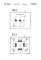
- the third embodiment shown in FIG. 4constitutes the preferred embodiment.
- Two oscillators 6a and 6bare perpendicular to each other and disposed side by side in a substantially peripheral zone of the membrane 2.
- the N and P channels of the oscillator 6aare perpendicular to the N and P channels respectively of the oscillator 6b.
- Temperature driftcan be practically eliminated by making the ratio of the frequencies delivered by the two oscillators.
- a possible improvementconsists in disposing four pairs of oscillators 6a and 6b, 6c and 6d, 6e and 6f, and 6g and 6h on respective ones of the four sides of a square membrane. Should it turn out that one, two, or even three of the pairs of oscillators are faulty for manufacturing reasons, there still remains a fourth pair of oscillators capable of constituting the sensor. The redundant nature of this improvement has the effect of increasing the yield of the manufacturing process very considerably. Further, it is highly advantageous since manufacturing cost is generally a function of the area of the silicon wafer being processed.
- Another possible improvementconsists in adding one or more oscillators 8a, 8c, 8e, and 8g disposed off the pressure sensitive membrane and serving to measure temperature so as to enable residual temperature drift to be corrected.
Landscapes
- Measuring Fluid Pressure (AREA)
- Resistance Heating (AREA)
Abstract
Description
Claims (7)
Applications Claiming Priority (2)
| Application Number | Priority Date | Filing Date | Title |
|---|---|---|---|
| FR8913338AFR2653197B1 (en) | 1989-10-12 | 1989-10-12 | METHOD FOR WATERPROOFING AN END OF AN ELECTRIC HEATING ELEMENT AND WATERPROOFING ELEMENT THROUGH THIS METHOD. |
| FR89133383 | 1989-10-13 |
Publications (1)
| Publication Number | Publication Date |
|---|---|
| US5281836Atrue US5281836A (en) | 1994-01-25 |
Family
ID=9386321
Family Applications (1)
| Application Number | Title | Priority Date | Filing Date |
|---|---|---|---|
| US07/844,616Expired - LifetimeUS5281836A (en) | 1989-10-12 | 1990-10-15 | Semiconductor sensor with perpendicular N and P-channel MOSFET's |
Country Status (2)
| Country | Link |
|---|---|
| US (1) | US5281836A (en) |
| FR (1) | FR2653197B1 (en) |
Cited By (11)
| Publication number | Priority date | Publication date | Assignee | Title |
|---|---|---|---|---|
| WO1996042111A1 (en)* | 1995-06-08 | 1996-12-27 | The Regents Of The University Of California | Cmos integrated microsensor with a precision measurement circuit |
| US5770803A (en)* | 1995-09-04 | 1998-06-23 | Honda Giken Kogyo Kabushiki Kaisha | Semiconductor stress sensor |
| US5895629A (en)* | 1997-11-25 | 1999-04-20 | Science & Technology Corp | Ring oscillator based chemical sensor |
| US6122975A (en)* | 1997-11-25 | 2000-09-26 | Institue Of Microelectronics | CMOS compatible integrated pressure sensor |
| US8132465B1 (en) | 2007-08-01 | 2012-03-13 | Silicon Microstructures, Inc. | Sensor element placement for package stress compensation |
| US20130342186A1 (en)* | 2010-12-22 | 2013-12-26 | Stmicroelectronics S.R.L. | Integrated electronic device for monitoring parameters within a solid structure and monitoring system using such a device |
| US20150117110A1 (en)* | 2013-10-31 | 2015-04-30 | Zhijiong Luo | Connecting storage gate memory |
| CN106323513A (en)* | 2015-06-30 | 2017-01-11 | 意法半导体股份有限公司 | Pressure sensor device for measuring a differential normal pressure to the device and related methods |
| CN106382883A (en)* | 2016-08-31 | 2017-02-08 | 珠海迈科智能科技股份有限公司 | Deformation detection method and device of printed circuit board (PCB) |
| US20220260437A1 (en)* | 2019-08-09 | 2022-08-18 | Sciosense B.V. | Electric Circuitry for Strain Measurement |
| US20220404217A1 (en)* | 2021-06-16 | 2022-12-22 | Robert Bosch Gmbh | Stress and/or strain measurement cell for a stress and/or strain measurement system |
Citations (9)
| Publication number | Priority date | Publication date | Assignee | Title |
|---|---|---|---|---|
| US3492861A (en)* | 1967-03-15 | 1970-02-03 | Csf | Strain gauge arrangement |
| US3624315A (en)* | 1967-01-23 | 1971-11-30 | Max E Broce | Transducer apparatus and transducer amplifier system utilizing insulated gate semiconductor field effect devices |
| FR2143553A1 (en)* | 1971-06-29 | 1973-02-09 | Sescosem | |
| GB2011707A (en)* | 1977-12-29 | 1979-07-11 | Teltov Geraete Regler | Silicon diaphragm with integrated piezo-resistant semi-conductor strain gauge elements. |
| JPS59117173A (en)* | 1982-12-23 | 1984-07-06 | Fujikura Ltd | Semiconductor pressure sensor |
| EP0040795B1 (en)* | 1980-05-22 | 1987-04-08 | Siemens Aktiengesellschaft | Semiconductor sensor |
| US4894698A (en)* | 1985-10-21 | 1990-01-16 | Sharp Kabushiki Kaisha | Field effect pressure sensor |
| US4965697A (en)* | 1988-03-30 | 1990-10-23 | Schlumberger Industries | Solid state pressure sensors |
| US5115292A (en)* | 1988-09-02 | 1992-05-19 | Honda Giken Kogyo Kabushiki Kaisha | Semiconductor sensor |
Family Cites Families (5)
| Publication number | Priority date | Publication date | Assignee | Title |
|---|---|---|---|---|
| DE1565337B1 (en)* | 1964-09-28 | 1970-10-22 | Bleckmann & Co | Tubular heater and process for its manufacture |
| DE3211484A1 (en)* | 1982-03-29 | 1983-09-29 | Stiebel Eltron Gmbh & Co Kg, 3450 Holzminden | Electrical tubular heating element |
| DE3400160A1 (en)* | 1984-01-04 | 1985-07-11 | Stiebel Eltron Gmbh & Co Kg, 3450 Holzminden | Method for producing a tubular radiator closure |
| DE3701453C2 (en)* | 1987-01-20 | 1995-11-30 | Conti Elektra Heizelemente | Electric tubular casing heater |
| DE8800261U1 (en)* | 1988-01-12 | 1988-02-25 | Elpag Ag Chur, Chur | Tubular radiator end closure |
- 1989
- 1989-10-12FRFR8913338Apatent/FR2653197B1/ennot_activeExpired - Lifetime
- 1990
- 1990-10-15USUS07/844,616patent/US5281836A/ennot_activeExpired - Lifetime
Patent Citations (9)
| Publication number | Priority date | Publication date | Assignee | Title |
|---|---|---|---|---|
| US3624315A (en)* | 1967-01-23 | 1971-11-30 | Max E Broce | Transducer apparatus and transducer amplifier system utilizing insulated gate semiconductor field effect devices |
| US3492861A (en)* | 1967-03-15 | 1970-02-03 | Csf | Strain gauge arrangement |
| FR2143553A1 (en)* | 1971-06-29 | 1973-02-09 | Sescosem | |
| GB2011707A (en)* | 1977-12-29 | 1979-07-11 | Teltov Geraete Regler | Silicon diaphragm with integrated piezo-resistant semi-conductor strain gauge elements. |
| EP0040795B1 (en)* | 1980-05-22 | 1987-04-08 | Siemens Aktiengesellschaft | Semiconductor sensor |
| JPS59117173A (en)* | 1982-12-23 | 1984-07-06 | Fujikura Ltd | Semiconductor pressure sensor |
| US4894698A (en)* | 1985-10-21 | 1990-01-16 | Sharp Kabushiki Kaisha | Field effect pressure sensor |
| US4965697A (en)* | 1988-03-30 | 1990-10-23 | Schlumberger Industries | Solid state pressure sensors |
| US5115292A (en)* | 1988-09-02 | 1992-05-19 | Honda Giken Kogyo Kabushiki Kaisha | Semiconductor sensor |
Non-Patent Citations (2)
| Title |
|---|
| Article by Neumeister et al., Jul. 1985, vol. 7, No. 3, Sensors and Actuators, pp. 167 175, A Silicon Pressure Sensor Using MOS Ring Oscillators .* |
| Article by Neumeister et al., Jul. 1985, vol. 7, No. 3, Sensors and Actuators, pp. 167-175, "A Silicon Pressure Sensor Using MOS Ring Oscillators". |
Cited By (17)
| Publication number | Priority date | Publication date | Assignee | Title |
|---|---|---|---|---|
| US5659195A (en)* | 1995-06-08 | 1997-08-19 | The Regents Of The University Of California | CMOS integrated microsensor with a precision measurement circuit |
| WO1996042111A1 (en)* | 1995-06-08 | 1996-12-27 | The Regents Of The University Of California | Cmos integrated microsensor with a precision measurement circuit |
| US5770803A (en)* | 1995-09-04 | 1998-06-23 | Honda Giken Kogyo Kabushiki Kaisha | Semiconductor stress sensor |
| US5895629A (en)* | 1997-11-25 | 1999-04-20 | Science & Technology Corp | Ring oscillator based chemical sensor |
| US6122975A (en)* | 1997-11-25 | 2000-09-26 | Institue Of Microelectronics | CMOS compatible integrated pressure sensor |
| US6263740B1 (en)* | 1997-11-25 | 2001-07-24 | Institute Of Microelectronics | CMOS compatible integrated pressure sensor |
| US8132465B1 (en) | 2007-08-01 | 2012-03-13 | Silicon Microstructures, Inc. | Sensor element placement for package stress compensation |
| US9097637B2 (en)* | 2010-12-22 | 2015-08-04 | Stmicroelectronics S.R.L. | Integrated electronic device for monitoring parameters within a solid structure and monitoring system using such a device |
| US20130342186A1 (en)* | 2010-12-22 | 2013-12-26 | Stmicroelectronics S.R.L. | Integrated electronic device for monitoring parameters within a solid structure and monitoring system using such a device |
| US20150117110A1 (en)* | 2013-10-31 | 2015-04-30 | Zhijiong Luo | Connecting storage gate memory |
| CN106323513A (en)* | 2015-06-30 | 2017-01-11 | 意法半导体股份有限公司 | Pressure sensor device for measuring a differential normal pressure to the device and related methods |
| CN106323513B (en)* | 2015-06-30 | 2019-11-26 | 意法半导体股份有限公司 | The pressure sensor apparatus and correlation technique of the difference normal pressure of measuring device |
| CN106382883A (en)* | 2016-08-31 | 2017-02-08 | 珠海迈科智能科技股份有限公司 | Deformation detection method and device of printed circuit board (PCB) |
| US20220260437A1 (en)* | 2019-08-09 | 2022-08-18 | Sciosense B.V. | Electric Circuitry for Strain Measurement |
| US12072254B2 (en)* | 2019-08-09 | 2024-08-27 | Sciosense B.V. | Electric circuitry with differently oriented ring oscillators for strain measurement |
| US20220404217A1 (en)* | 2021-06-16 | 2022-12-22 | Robert Bosch Gmbh | Stress and/or strain measurement cell for a stress and/or strain measurement system |
| US11971316B2 (en)* | 2021-06-16 | 2024-04-30 | Robert Bosch Gmbh | Direction-dependent stress and/or strain measurement cell for a stress and/or strain measurement system |
Also Published As
| Publication number | Publication date |
|---|---|
| FR2653197B1 (en) | 1991-12-27 |
| FR2653197A1 (en) | 1991-04-19 |
Similar Documents
| Publication | Publication Date | Title |
|---|---|---|
| US4420790A (en) | High sensitivity variable capacitance transducer | |
| US5281836A (en) | Semiconductor sensor with perpendicular N and P-channel MOSFET's | |
| US4680606A (en) | Semiconductor transducer | |
| KR900004369B1 (en) | Semiconductor strain gauge bridge circuit | |
| EP1316786A1 (en) | Capacity type pressure sensor and method of manufacturing the pressure sensor | |
| US4990986A (en) | Semiconductor acceleration sensor | |
| US6683358B1 (en) | Silicon integrated accelerometer | |
| US4861420A (en) | Method of making a semiconductor transducer | |
| US4191057A (en) | Inversion layer sprain gauge | |
| US4050313A (en) | Semiconductor pressure transducer | |
| KR100200938B1 (en) | Semiconductor sensor | |
| JPH0241184B2 (en) | ||
| US8984953B2 (en) | Solid state pressure sensor | |
| JPH11148946A (en) | Integration acceleration sensor | |
| JPH11304618A (en) | Semiconductor strain sensor | |
| JP2864700B2 (en) | Semiconductor pressure sensor and method of manufacturing the same | |
| RU2050033C1 (en) | Integral tension transducer | |
| Yang et al. | A CMOS stress sensor chip with integrated signal processing circuits | |
| JP3093216B2 (en) | Semiconductor device and inspection method thereof | |
| JP2661528B2 (en) | Semiconductor integrated circuit device | |
| JP3084616B2 (en) | Diffusion type pressure transducer | |
| JPH04247667A (en) | Semiconductor pressure sensor | |
| EP1019968B1 (en) | Method for manufacturing a diode device having a low threshold voltage | |
| JP2985462B2 (en) | Semiconductor pressure gauge | |
| CA1271049A (en) | Semiconductor transducer |
Legal Events
| Date | Code | Title | Description |
|---|---|---|---|
| AS | Assignment | Owner name:SCHLUMBERGER INDUSTRIES, FRANCE Free format text:ASSIGNMENT OF ASSIGNORS INTEREST.;ASSIGNORS:MOSSER, VINCENT;SUSKI, JAN;REEL/FRAME:006234/0894 Effective date:19920331 | |
| STCF | Information on status: patent grant | Free format text:PATENTED CASE | |
| FEPP | Fee payment procedure | Free format text:PAYOR NUMBER ASSIGNED (ORIGINAL EVENT CODE: ASPN); ENTITY STATUS OF PATENT OWNER: LARGE ENTITY | |
| FPAY | Fee payment | Year of fee payment:4 | |
| FPAY | Fee payment | Year of fee payment:8 | |
| AS | Assignment | Owner name:SCHLUMBERGER ELECTRICITY, INC., SOUTH CAROLINA Free format text:ASSIGNMENT OF ASSIGNORS INTEREST;ASSIGNOR:SCHLUMBERGER SA;REEL/FRAME:014499/0598 Effective date:20030317 Owner name:SCHLUMBERGER SA, FRANCE Free format text:CHANGE OF NAME;ASSIGNOR:SCHLUMBERGER INDUSTRIES, SA;REEL/FRAME:014499/0586 Effective date:20021226 | |
| AS | Assignment | Owner name:WELLS FARGO BANK, NATIONAL ASSOCIATION, AS ADMINIS Free format text:SECURITY AGREEMENT;ASSIGNOR:SCHLUMBERGER ELECTRICITY, INC.;REEL/FRAME:014822/0327 Effective date:20040701 | |
| AS | Assignment | Owner name:ITRON ELECTRICITY METERING, INC., SOUTH CAROLINA Free format text:CHANGE OF NAME;ASSIGNOR:SCHLUMBERGER ELECTRICITY, INC.;REEL/FRAME:014863/0313 Effective date:20040716 | |
| AS | Assignment | Owner name:WELLS FARGO BANK, NATIONAL ASSOCIATION, AS ADMINIS Free format text:AMENDMENT TO GRANTOR NAME CHANGE UNDER SECURITY AGREEMENT;ASSIGNOR:ITRON ELECTRICITY METERING, INC.;REEL/FRAME:015312/0692 Effective date:20041005 | |
| FEPP | Fee payment procedure | Free format text:PAYER NUMBER DE-ASSIGNED (ORIGINAL EVENT CODE: RMPN); ENTITY STATUS OF PATENT OWNER: LARGE ENTITY Free format text:PAYOR NUMBER ASSIGNED (ORIGINAL EVENT CODE: ASPN); ENTITY STATUS OF PATENT OWNER: LARGE ENTITY | |
| FPAY | Fee payment | Year of fee payment:12 | |
| AS | Assignment | Owner name:ITRON, INC., WASHINGTON Free format text:MERGER;ASSIGNOR:ITRON ELECTRICITY METERING, INC.;REEL/FRAME:017025/0439 Effective date:20060101 | |
| AS | Assignment | Owner name:WELLS FARGO BANK, NATIONAL ASSOCIATION,WASHINGTON Free format text:SECURITY AGREEMENT;ASSIGNOR:ITRON, INC.;REEL/FRAME:019204/0544 Effective date:20070418 Owner name:WELLS FARGO BANK, NATIONAL ASSOCIATION, WASHINGTON Free format text:SECURITY AGREEMENT;ASSIGNOR:ITRON, INC.;REEL/FRAME:019204/0544 Effective date:20070418 | |
| AS | Assignment | Owner name:ITRON, INC., CALIFORNIA Free format text:TERMINATION AND RELEASE OF SECURITY INTEREST IN INTELLECTUAL PROPERTY;ASSIGNOR:WELLS FARGO BANK, NATIONAL ASSOCIATION;REEL/FRAME:019466/0486 Effective date:20070418 | |
| AS | Assignment | Owner name:ITRON, INC., WASHINGTON Free format text:RELEASE BY SECURED PARTY;ASSIGNOR:WELLS FARGO BANK, NATIONAL ASSOCIATION;REEL/FRAME:026749/0263 Effective date:20110805 |