US5281798A - Method and system for selective removal of material coating from a substrate using a flashlamp - Google Patents
Method and system for selective removal of material coating from a substrate using a flashlampDownload PDFInfo
- Publication number
- US5281798A US5281798AUS07/813,864US81386491AUS5281798AUS 5281798 AUS5281798 AUS 5281798AUS 81386491 AUS81386491 AUS 81386491AUS 5281798 AUS5281798 AUS 5281798A
- Authority
- US
- United States
- Prior art keywords
- radiant energy
- reflected
- set forth
- prescribed
- intensity
- Prior art date
- Legal status (The legal status is an assumption and is not a legal conclusion. Google has not performed a legal analysis and makes no representation as to the accuracy of the status listed.)
- Expired - Fee Related
Links
Images


Classifications
- B—PERFORMING OPERATIONS; TRANSPORTING
- B23—MACHINE TOOLS; METAL-WORKING NOT OTHERWISE PROVIDED FOR
- B23K—SOLDERING OR UNSOLDERING; WELDING; CLADDING OR PLATING BY SOLDERING OR WELDING; CUTTING BY APPLYING HEAT LOCALLY, e.g. FLAME CUTTING; WORKING BY LASER BEAM
- B23K26/00—Working by laser beam, e.g. welding, cutting or boring
- B23K26/02—Positioning or observing the workpiece, e.g. with respect to the point of impact; Aligning, aiming or focusing the laser beam
- B23K26/03—Observing, e.g. monitoring, the workpiece
- B23K26/032—Observing, e.g. monitoring, the workpiece using optical means
- B—PERFORMING OPERATIONS; TRANSPORTING
- B08—CLEANING
- B08B—CLEANING IN GENERAL; PREVENTION OF FOULING IN GENERAL
- B08B7/00—Cleaning by methods not provided for in a single other subclass or a single group in this subclass
- B08B7/0035—Cleaning by methods not provided for in a single other subclass or a single group in this subclass by radiant energy, e.g. UV, laser, light beam or the like
- B08B7/0042—Cleaning by methods not provided for in a single other subclass or a single group in this subclass by radiant energy, e.g. UV, laser, light beam or the like by laser
- B—PERFORMING OPERATIONS; TRANSPORTING
- B23—MACHINE TOOLS; METAL-WORKING NOT OTHERWISE PROVIDED FOR
- B23K—SOLDERING OR UNSOLDERING; WELDING; CLADDING OR PLATING BY SOLDERING OR WELDING; CUTTING BY APPLYING HEAT LOCALLY, e.g. FLAME CUTTING; WORKING BY LASER BEAM
- B23K26/00—Working by laser beam, e.g. welding, cutting or boring
- B23K26/12—Working by laser beam, e.g. welding, cutting or boring in a special atmosphere, e.g. in an enclosure
- B23K26/123—Working by laser beam, e.g. welding, cutting or boring in a special atmosphere, e.g. in an enclosure in an atmosphere of particular gases
- B—PERFORMING OPERATIONS; TRANSPORTING
- B23—MACHINE TOOLS; METAL-WORKING NOT OTHERWISE PROVIDED FOR
- B23K—SOLDERING OR UNSOLDERING; WELDING; CLADDING OR PLATING BY SOLDERING OR WELDING; CUTTING BY APPLYING HEAT LOCALLY, e.g. FLAME CUTTING; WORKING BY LASER BEAM
- B23K26/00—Working by laser beam, e.g. welding, cutting or boring
- B23K26/14—Working by laser beam, e.g. welding, cutting or boring using a fluid stream, e.g. a jet of gas, in conjunction with the laser beam; Nozzles therefor
- B23K26/142—Working by laser beam, e.g. welding, cutting or boring using a fluid stream, e.g. a jet of gas, in conjunction with the laser beam; Nozzles therefor for the removal of by-products
- B—PERFORMING OPERATIONS; TRANSPORTING
- B23—MACHINE TOOLS; METAL-WORKING NOT OTHERWISE PROVIDED FOR
- B23K—SOLDERING OR UNSOLDERING; WELDING; CLADDING OR PLATING BY SOLDERING OR WELDING; CUTTING BY APPLYING HEAT LOCALLY, e.g. FLAME CUTTING; WORKING BY LASER BEAM
- B23K26/00—Working by laser beam, e.g. welding, cutting or boring
- B23K26/36—Removing material
- B23K26/40—Removing material taking account of the properties of the material involved
- B—PERFORMING OPERATIONS; TRANSPORTING
- B44—DECORATIVE ARTS
- B44D—PAINTING OR ARTISTIC DRAWING, NOT OTHERWISE PROVIDED FOR; PRESERVING PAINTINGS; SURFACE TREATMENT TO OBTAIN SPECIAL ARTISTIC SURFACE EFFECTS OR FINISHES
- B44D3/00—Accessories or implements for use in connection with painting or artistic drawing, not otherwise provided for; Methods or devices for colour determination, selection, or synthesis, e.g. use of colour tables
- B44D3/16—Implements or apparatus for removing dry paint from surfaces, e.g. by scraping, by burning
- B44D3/166—Implements or apparatus for removing dry paint from surfaces, e.g. by scraping, by burning by heating, e.g. by burning
- G—PHYSICS
- G01—MEASURING; TESTING
- G01N—INVESTIGATING OR ANALYSING MATERIALS BY DETERMINING THEIR CHEMICAL OR PHYSICAL PROPERTIES
- G01N21/00—Investigating or analysing materials by the use of optical means, i.e. using sub-millimetre waves, infrared, visible or ultraviolet light
- G01N21/84—Systems specially adapted for particular applications
- G01N21/8422—Investigating thin films, e.g. matrix isolation method
- B—PERFORMING OPERATIONS; TRANSPORTING
- B23—MACHINE TOOLS; METAL-WORKING NOT OTHERWISE PROVIDED FOR
- B23K—SOLDERING OR UNSOLDERING; WELDING; CLADDING OR PLATING BY SOLDERING OR WELDING; CUTTING BY APPLYING HEAT LOCALLY, e.g. FLAME CUTTING; WORKING BY LASER BEAM
- B23K2101/00—Articles made by soldering, welding or cutting
- B23K2101/34—Coated articles, e.g. plated or painted; Surface treated articles
- B23K2101/35—Surface treated articles
- B—PERFORMING OPERATIONS; TRANSPORTING
- B23—MACHINE TOOLS; METAL-WORKING NOT OTHERWISE PROVIDED FOR
- B23K—SOLDERING OR UNSOLDERING; WELDING; CLADDING OR PLATING BY SOLDERING OR WELDING; CUTTING BY APPLYING HEAT LOCALLY, e.g. FLAME CUTTING; WORKING BY LASER BEAM
- B23K2103/00—Materials to be soldered, welded or cut
- B23K2103/16—Composite materials, e.g. fibre reinforced
- B—PERFORMING OPERATIONS; TRANSPORTING
- B23—MACHINE TOOLS; METAL-WORKING NOT OTHERWISE PROVIDED FOR
- B23K—SOLDERING OR UNSOLDERING; WELDING; CLADDING OR PLATING BY SOLDERING OR WELDING; CUTTING BY APPLYING HEAT LOCALLY, e.g. FLAME CUTTING; WORKING BY LASER BEAM
- B23K2103/00—Materials to be soldered, welded or cut
- B23K2103/30—Organic material
- B23K2103/42—Plastics
- B—PERFORMING OPERATIONS; TRANSPORTING
- B23—MACHINE TOOLS; METAL-WORKING NOT OTHERWISE PROVIDED FOR
- B23K—SOLDERING OR UNSOLDERING; WELDING; CLADDING OR PLATING BY SOLDERING OR WELDING; CUTTING BY APPLYING HEAT LOCALLY, e.g. FLAME CUTTING; WORKING BY LASER BEAM
- B23K2103/00—Materials to be soldered, welded or cut
- B23K2103/50—Inorganic material, e.g. metals, not provided for in B23K2103/02 – B23K2103/26
- B23K2103/52—Ceramics
- G—PHYSICS
- G01—MEASURING; TESTING
- G01J—MEASUREMENT OF INTENSITY, VELOCITY, SPECTRAL CONTENT, POLARISATION, PHASE OR PULSE CHARACTERISTICS OF INFRARED, VISIBLE OR ULTRAVIOLET LIGHT; COLORIMETRY; RADIATION PYROMETRY
- G01J3/00—Spectrometry; Spectrophotometry; Monochromators; Measuring colours
- G01J3/46—Measurement of colour; Colour measuring devices, e.g. colorimeters
- G01J3/50—Measurement of colour; Colour measuring devices, e.g. colorimeters using electric radiation detectors
- G01J3/51—Measurement of colour; Colour measuring devices, e.g. colorimeters using electric radiation detectors using colour filters
Definitions
- the present inventionrelates to a material removal process and system, and more particularly, to a material removal process and system that uses pulsed light from a flashlamp, or equivalent pulsed high energy light source (such as a laser), to ablate the material to be removed; and also uses optical feedback from the surface being ablated to determine when the proper amount of material has been removed.
- a flashlampor equivalent pulsed high energy light source (such as a laser)
- optical feedbackfrom the surface being ablated to determine when the proper amount of material has been removed.
- Coatingsplay an important role in our manufactured products based society. Coatings provide immunity to corrosion, thermal insulation, shielding, as well as appearance enhancement, and an aid in identification.
- PMBparticle medium blast
- PMB methodsthat are energetic enough by themselves to remove hardened coatings such as paint may damage delicate surfaces such as are found on aircraft and automobiles if they are not carefully managed. For example, if the impinging particles dwell too long at one location, the impinged surface may become pitted or stress hardened. This is especially important with regard to the surfaces of aircraft since pitting or stress hardening may change the loading on that portion of the aircraft. PMB may also damage putty joints often found on aircraft between surface plates.
- Radiant energy paint removal techniquesare likewise known in the art.
- One such systemuses a laser and video frame grabber in a video controlled paint removal system in which paint is stripped from a surface using the output of the laser to ablate the paint while a video camera converts images of the surface being stripped into electronic data signals. The data signals are used to control the laser output.
- a processorcompares the data signals with parameters stored in a memory to determine whether sufficient paint has been removed from the surface being stripped If an insufficient amount of paint has been removed, then the surface continues being irradiated by the laser. If the irradiated area has been adequately stripped, the processor directs the laser to ablate another area.
- the difficulty associated with removing paint or other coatingsis compounded when the basic substrate material over which the coating has been placed is non-metallic.
- composite structuresare becoming increasingly more common.
- Such structuresare typically manufactured, for example, of fiber reinforced epoxy or other thermoset or thermoplastic composites.
- Many aircraft and automobilesextensively employ plastic composites for surface structures.
- Such structuresare painted for a variety of reasons including aesthetics, identification, and camouflage.
- Such painted surfacesdeteriorate under the action of weather and the mechanical forces to which they are subjected, thus requiring removal and replacement.
- other than hand sandingthere are no suitable methods for removing paint from the surfaces of such composites.
- the present inventionadvantageously provides a system and method for removing paint, or similar coatings, that address the above and other needs.
- pulsed light sourcesare used to remove coatings from substrates via the ablation method.
- ablationis defined as the rapid decomposition and vaporization of a material resulting from the absorption of energy by the material and is associated with the generation of pressure waves radiating from the surface of the material.
- the amount of material removed by the ablative process of the inventionis controlled using a photodetector system that measures the color intensity of the light reflected from the substrate at the particular location where the material is being removed.
- the photodetector systemis able to readily ascertain in real time when the topcoat(s) has been removed and only the primer undercoat remains, or when all the upper coats have been removed and only the substrate surface remains.
- a pulsed light source in combination with a photodetector systemis scanned across a work surface in a controlled manner so as to systematically remove all coatings on the work surface down to a prescribed color.
- a prescribed colormay advantageously be that of a prescribed undercoat, e.g., the primer coat, or that of the substrate.
- the feedback provided by the photodetector systemmay also be used to indicate the character of the stripped work surface for quality control purposes.
- the photodetector systemmay sense position information on the work surface, which position information may be used by a robotic controller to control the scanning operation.
- the coating removal system of the inventionincludes an ablation removal device, such as a flashlamp or a laser, and a photodetecting circuit, housed within a single scanning head.
- a flashlamp, or flashtubeis a gas filled device which converts electrical energy to optical energy by passing current through a plasma typically contained in a transparent tube through which the optical energy is transmitted.
- the output signal(s) from the photodetecting circuitis (are) used as a feedback signal(s) to provide optical feedback to the circuits that control and position the ablation removal device, thereby enabling the scanning head to be effectively scanned across the work surface at a rate and with an incident intensity of the surface that efficiently and safely removes a desired coating from the work surface without damaging the work surface.
- the photodetecting circuit of the inventionincludes at least one array of photodiodes.
- the photodiodes of each arrayare optically filtered so as to detect a prescribed wavelength, or band of wavelengths, representing a desired color, e.g., one of the primary colors, or other selected color.
- the photodiodes of each arrayare positioned so as to monitor reflected light energy from the work surface.
- the photodiode arraysare gated ON only at a time that allows them to sense or collect light energy associated with a trailing edge portion of the main optical pulse generated by the ablative device.
- a secondary or auxiliary light source within the scanning headmay be pulsed ON at an appropriate time within the ablative removal cycle to adequately illuminate the work surface with sufficient viewing light to provide a source of reflected light suitable for detection by the photodiodes in the array.
- the electrical signals generated by the photodiodes in response to sensing the reflected light of each arrayare converted to digital sensor data and processed by digital circuitry in a sensor controller.
- Parallel monitoring of the optical output from the ablative removal deviceprovides a basis for normalizing the optical information from the photodiode arrays.
- the normalized sensor datais then temporarily stored and compared with permanently stored reference data representative of the desired color of the work surface once the prescribed coating has been removed therefrom.
- the results of this comparisonform a basis for a feedback signal directed to a remote computerized controller. That is, since different coating layers as well as substrates are characterized by different colors and reflected optical intensities, the feedback signal affords a method for real time control of the coating removal process and allows selective removal of successive coating layers.
- the feedback signalmay be acted upon by the remote computerized controller in order to control the ablation removal process in a desired manner.
- the output signals from the one or more of the photodetector arraysallow optical information from the entire width of the irradiated surface on the structure to be processed.
- the area irradiated by the light source when the scan speed is zerois referred to as the "footprint.”
- Optical information reflected from the "footprint”advantageously provides increased spatial resolution and sensitivity of the system to coating anomalies, e.g., repair patches on an aircraft skin that may have been hidden by subsequent over coats of paint.
- such spatial capabilityprovides a means for assisting a robotic controller, or equivalent positioning device controlled by the remote computerized controller, in maintaining the scanning head in a prescribed orientation, e.g., a level position, above the work surface.
- appropriate cooling meansfor limiting the temperature of the structure in the vicinity of the irradiated area is also included within the scanning head.
- Such cooling meanstypically includes a nozzle for directing a particle stream, e.g., a jet of CO 2 pellets, at the area from which material has been ablated, as well as an appropriate vacuum system for removing all expended particles, gases, and vapors associated with the ablative removal process.
- the particle streamalso advantageously cleans the ablated surface.
- the present inventionmay be characterized, in accordance with one embodiment thereof, as a method for removing material from a structure.
- Such methodincludes the steps of (1) irradiating a target area of a structure having at least one layer of material formed on a substrate with radiant energy having an intensity sufficient to ablate the layer of material; (2) monitoring reflected radiant energy from the target area to sense the presence of a prescribed color intensity different from the color intensity of the layer of material being ablated; and (3) controlling the irradiation of the target area with the radiant energy in step (1) as a function of the color intensity sensed in step (2).
- the present inventionmay be characterized as a system for removing a layer of material from a structure.
- Such systemincludes: (a) irradiating means for irradiating a target area of a structure having at least one layer of material formed on a substrate with radiant energy having an intensity sufficient to ablate the layer of material; (b) monitoring means for monitoring reflected radiant energy from the target area for the presence of a prescribed color intensity different from the color intensity of the layer of material being ablated by the irradiating means; and (c) feedback means for controlling the irradiation of the target area with the radiant energy from the irradiating means as a function of the color intensity sensed by the monitoring means.
- photodetection meansdetects reflected radiant energy having a prescribed wavelength, where the prescribed wavelength is characteristic of the prescribed color.
- photodetection meansincludes: (a) means for dividing the reflected radiant energy into a plurality of optical channels; (b) first detection means for detecting if the reflected radiant energy in each of the plurality of channels contains a respective wavelength; and (c) processor means for analyzing the respective wavelengths detected in each optical channel to ascertain whether the prescribed color intensity is present in the reflected radiant energy.
- Still a further embodiment of the inventionmay be characterized as photodetector apparatus useful for examining the surface of a structure.
- Such photodetector apparatusincludes: (a) illuminating means for illuminating a target area of the surface of the structure with pulsed radiant energy; and (b) monitoring means for monitoring reflected radiant energy from the target area for the presence of a prescribed color intensity.
- radiant energy ablative removal meanssuch as a flashlamp
- photodetector meansfor optically detecting when a desired coating has been stripped from the work surface
- cooling and cleaning meansfor limiting the temperature of the structure and for removing any residue of the ablated material from the stripped work surface.
- such scanning headmay be scanned across the work surface as a function of feedback signals sensed by the photodetector means.
- Such photodetector output signal(s)provide an indication of the color intensity of the work surface, which indication may advantageously be used for varied purposes.
- such output signal(s)may be used as a feedback signal(s) for one or more of the following purposes: (1) to control the coating removal process, i.e., to limit the exposure of the stripped surfaces or layers, thereby preventing damage to the work surface or coating layers; (2) to position and orient, e.g., level, the ablative removal system above a desired location on the work surface relative to topological landmarks on the work surface; (3) to enable the safe and efficient operation of the ablative removal device, as by, e.g., turning on the ablative removal device only when certain conditions are satisfied, and/or by controlling the output power of the radiated energy generated by the ablative removal device; (4) to provide real time feedback to a remote controller that controls the scan rate of the ablative removal device; or (5) to monitor the formation of frost and/or condensation on the work surface from the application of a particle stream, which particle stream may be used to cool and clean the structure.
- the output signal(s) from the photodetector systemmay also be used, for example, to monitor a previously stripped section of the work surface for the purpose of quality control or surface anomaly detection.
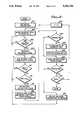
- FIG. 1is a block diagram that diagrammatically illustrates the main components of a coating removal system made in accordance with the present invention
- FIG. 2is a schematic diagram of the scanning head used with the coating removal system shown in FIG. 1;
- FIG. 3is a block diagram of the photodetector circuit
- FIG. 4is a waveform timing diagram that illustrates one timing arrangement that may be used for operating the photodetector circuit in accordance with the present invention
- FIG. 5is a waveform timing diagram that illustrates an alternative timing arrangement for operating the photodetector circuit
- FIG. 6is a diagrammatic representation of one embodiment of the photodetector arrays
- FIG. 7shows a diagrammatic representation of an alternative embodiment of a photodetector array of the present invention.
- FIG. 8is a flow chart that depicts the basic method used by the system shown of FIG. 1 to remove coatings from a substrate.
- the present inventioncombines an ablative removal technique with a particular optical detection technique in order to remove one or more coatings from a substrate surface.
- Ablative removal techniques using radiant energye.g., a flashlamp, combined with a different type of detection system, are described in applicants' copending application entitled “Method and System for Control of a Material Removal Process Using Spectral Emission Discrimination", Ser. No. 07/813,865, filed concurrently herewith.
- FIG. 1there is shown a block diagram that diagrammatically illustrates the main components of a coating removal system 11 made in accordance with the present invention.
- the system 11removes coatings 24 and/or 26 from a substrate 28 without damaging the substrate.
- the coated substrate 28may hereafter be referred to as the "work surface” or "structure” 22.
- the system 11includes a digital control processor 200 that coordinates and controls the scan rate of optical energy 18 and particle stream 30 across the surface of substrate 22. Control is effected using feedback provided by an optical detecting circuit 100 that detects the optical character of the surface of the work surface 22.
- data processor 200(which may be an IBM AT or AT compatible personal computer, or equivalent) generates output signal 5 to enable particle stream source 6, output signal 7 to enable vacuum system 37, output control signal 12 to control light control circuit 13 (which may be of a type well known by those skilled in the art), and output signal 202 to provide path and speed instructions to robotic controller 204.
- Particle stream source 6in turn, is coupled to nozzle 32, which nozzle is adapted to direct a stream 30 of particles, explained more fully below, across the surface of the workpiece 22.
- vacuum system 37is coupled to exhaust nozzle 36, which exhaust nozzle is positioned to receive the residue 45 of any materials that are ablated by radiant energy 18 generated by ablative light source 14 and/or the spent particle stream.
- Light control circuit 13generates a control signal 15 which establishes the repetition rate and pulse width of the output of ablative light source 14. In some embodiments of the invention, light control circuit 13 also generates another control signal 17 which turns on auxiliary light 29 for a desired time period during the coating removal cycle, as explained more fully below in connection with FIG. 5.
- Nozzle 32, ablative light source 14, auxiliary light source 29 (when used), and exhaust nozzle 36are all housed within a scanning head assembly 10 that is adapted to move above the work surface 22 as controlled by robotic positioner 19, as indicated by the arrow 21.
- electrical, optical, and other coupling to the elements within the scanning head assembly 10is achieved through appropriate flexible cabling 31, thereby facilitating movement of the scanning head assembly, including the elements housed therein, while allowing the control circuits for such elements, such as the particle stream source 6, the light control circuit 13, and the vacuum system 37, to be stationary at a position remote from the scanning head assembly 10.
- a photodetecting circuit 100detects the optical condition at the work surface 22 by monitoring radiant energy 27 reflected from the work surface 22.
- the photodetecting circuit 100receives the optical signals and generates electrical feedback signal(s) 194 therefrom that are conveyed to the control processor 200.
- the control processor 200processes the feedback signals 194 and converts them into a composite output signal 202.
- Robotic controller 204transforms signal 202 into control or instructional signals 206 that direct the path and speed of robotic positioner 19.
- Such instruction signal 206directs robotic positioner 19 to move the scanning head assembly across the work surface 22 so as to effectively scan ablative energy source 14 and particle stream 30 across the surface of the structure 22 in accordance with a prescribed pattern.
- the path of robotic controller 204is determined in accordance with a suitable path generating processing routine implemented by data processor 200 in accordance with techniques well known by those skilled in the art.
- photodetector circuit 100is preferably located within or attached to the scanning assembly 10, with the output signal 194 of the photodetector circuit 100 being coupled to the remotely positioned control processor 200 through appropriate flexible electrical cable.
- FIG. 2there is shown a schematic diagram of the scanning head assembly 10 used with the coating removal system 11.
- the scanning head assembly 10comprising optical energy source 14 and reflector 16, is supported by robotic positioner 13 at a predetermined standoff distance "d" from the surface of structure 22.
- the optimum standoff distance "d" for ablative removal of coatingsis a function of the amount of output power contained in the radiant energy 18 output by the ablative energy source 14. In general, the closer the source 14 is positioned to the work surface 22, the more power there is to ablate the upper coatings 24 and/or 26 covering the substrate 28. However, care must be exercised to prevent too much ablative power from being delivered, else more than the desired coating(s) may be ablated.
- the ablative powermay be controlled by adjusting the repetition frequency and pulse width of the light 18 generated by the light source 14, the intensity of optical energy 18 incident on the surface of structure 22 is preferably controlled by simply controlling the standoff distance "d” . Initially, an approximate distance "d" for nominal output power levels of the light source 14 is determined experimentally.
- the ablative energy sourceis a flashlamp, as described in applicants' copending applications referenced above, and where such flashlamp provides an incident intensity at the surface of the structure of about 1-10 joules/cm 2 and has a pulse width that may range from about 1000-2400 microseconds ( ⁇ sec) and a repetition rate of 4-5 Hz, and further where a coating of paint having a nominal thickness of 4-8 mils overlays an aluminum substrate, the initial standoff distance "d" is on the order of 1 to 3 cm.
- Robotic positioner 19is controlled to move the assembly 10 along a predetermined path at a controlled scan speed over the surface of structure 22 so that ablative energy source 14 and particle stream 30 may be directed to scan and impinge, respectively, the coating or coatings formed on the surface of substrate 28.
- the radiant energy (light) 18 from the source 14ablates the coating to be removed in the immediate area of exposure to the radiant energy 18.
- the particle stream 30limits the temperature rise of structure 22 as a result of absorbing optical energy in the form of heat provided by light 18.
- Robotic positioner 19may be implemented as a CIMROC 4000 Robot Controller manufactured by CIMCORP Precision Systems, Inc., Shoreview, Minn.
- the scan speedis functionally related to the output signal 194 by a function bounded by upper and lower limits, as described more fully in the referenced patent application. Such function may be increasing or decreasing, depending on the particular application.
- Material removed from the surface of substrate 28 and the expended particle stream 30 after it impinges structure 22are collected by vacuum system 37 through nozzle 25 mounted to housing 12.
- Particle stream 30is provided by particle stream source 6 which may provide gas, liquid, or solid particles, or any combination of particles.
- particle stream source 6may be a gas tank if particle stream 30 is a gas, or a carbon dioxide pellet source of the type commercially available from Cold Jet, Inc., of Loveland, Ohio.
- the particles which comprise particle stream 30are delivered to nozzle 32 via duct 34.
- the system 11is configured to remove an upper layer 24 from the substrate 28 while leaving a lower layer 26, e.g., a primer paint coat. Such removal is only exemplary, as the system 11 could just as easily be configured to remove both layers 24 and 26, leaving the surface of the substrate 28 exposed.
- the mechanism by which the system 11 determines when the proper layer has been ablatively removedis to monitor light 27 reflected from the surface 22 for a specific color and intensity, i.e., color intensity. Such monitoring assumes, of course, that a distinguishing color intensity difference exists between the layer 26 to be removed and the layer 24 to remain, or between the layers 24 and 26 to be removed and the substrate surface. This assumption will almost always be true.
- the reflected light 27is detected, collected, and analyzed by photodetector circuit 100.
- the reflected light that is monitoredmay be either the trailing edge of the ablative light pulse 18, as explained more fully below in connection with FIG. 4, or light obtained from an auxiliary light source 29, as explained more fully below in connection with FIG. 5.
- the reflected lightis monitored by the photodetector circuit 100 for the presence of a specific wavelength, or a band of wavelengths, characteristic of the color of the layer or surface that is to remain.
- the control processor 200is notified via the signal 194 so that it knows that sufficient material has been removed at the present location of the incident radiant energy 18.
- the control processor 200immediately generates the requisite control signals so as to move the scanning head 10 to a new location, adjust the scanning speed, and/or adjust the output power of the light source 14, in order to assure that no further material is removed at the location where the characteristic wavelength was detected.
- photodetector circuit 100is attached to the outside of a water cooled housing 12 wherein the light source 14 is housed. Water, or other suitable coolant, enters and exits the housing 12 through parts 44 and 46. Photodetector circuit 100 is mounted to the exterior of housing 12 such that it is able to detect reflected light 27 from the surface of structure 22.
- the particle stream 30, directed at the surface 22 at an approximate angle ⁇helps to keep the lens cover 20 of the housing 12 clean from debris and other foreign matter that might otherwise accumulate thereon.
- the angle ⁇will typically range from 5 to 60 degrees, but is not felt to be critical for ablation as described herein.
- Photodetector circuit 100should be oriented to receive reflected light from immediately behind the same area impinged by the incident ablative light source 18.
- the reflected footprint areai.e., that area from which the reflected light 27 is received, actually be somewhat larger and behind the irradiated footprint.
- the irradiated footprintmay be referred to as the "target area” because it is the area at which incident light 18 is directed.
- the photodetector circuit 100have spatial distribution resolution capabilities so that it can detect not only the presence of a characteristic wavelength, but also a particular narrow area or region within the monitored area whereat the characteristic wavelength originated.
- Such spatial distribution resolutionis advantageously provided by using a plurality of photodetectors arranged in a suitable pattern within a photodetector array, as described more fully below in conjunction with FIGS. 6 and 7.
- a preferred ablative light source 14is a water-cooled flashlamp that is housed within a custom housing as described in the cited patent applications.
- a suitable flashlamp for use within such a housingis available from Maxwell Laboratories, Inc., of San Diego, Calif., and is described in commonly assigned U.S. patent application Ser. No. 07/645,372, filed Jan. 24, 1991 U.S. Pat. No. 5,126,621, which patent application is also incorporated herein by reference.
- the photodetector circuit 100will next be described. It is the function of the photodetecting circuit 100 to detect the optical character of the surface of structure 22.
- the photodetector circuit 100simply includes a single photodiode selected to detect a particular characteristic wavelength. Wavelength selection is made by choosing a particular photodiode/lens/filter combination (which are commercially available components), or by selecting a broadband photodiode and manually placing a removable or replaceable filter in the optical path leading to the photodiode. In this manner, only optical signals of the characteristic wavelength successfully pass through the filters and are detected by the photodiode. All other optical signals are blocked by the filter.
- a blue filtermay be placed in front of the photodiode so that the photodiode only detects blue light. If a subsequent coating removal operation requires that all layers be removed down to the substrate, and if the substrate is, e.g., yellow, then the blue filter may be removed and replaced with a yellow filter., i.e., a filter, or combination of filters, that only allows yellow light to pass therethrough.
- a single photodiodeas the photodetecting circuit 100 only provides limited resolution of the reflected light to be analyzed, and does not provide additional information, such as spatial distribution data, that may be detected. Hence, it is preferred that more than one photodiode be used, and that an appropriately processed optical, digital output signal 194 be generated from all of such photodiodes. For example, a digital weighted sum average (“WSAV”) signal may be generated from all of the output signals from the individual photodiodes in the array.
- FIG. 3A block diagram of one type of photodetector circuit 100 that achieves this function is shown in FIG. 3. As seen in FIG. 3, the reflected light 27 from the surface 22 is received by filters 102. As seen in FIG.
- processor 148may be realized using any suitable microprocessor circuit capable of operating at a modest clock speed, e.g., 5-10 MHz.
- processor 148may be implemented using an Intel 8X51FB imbedded processor.
- RAMrandom access memory
- ROMread only memory
- A/Danalog-to-digital converter
- MUXanalog multiplex circuit
- the channelsmay be respectively designed to receive and process wavelengths characteristic of the color intensities associated with red, blue or yellow.
- photodetecting system 100is able to receive and analyze optical energy intensities from selected portions, or from all, of the entire optical portion of the electromagnetic spectrum.
- the optical data received in each data channelis filtered and continuously monitored by photodiodes contained in the photodiode arrays 106, 118 or 130, and is temporarily stored in response to receiving an appropriate clock or shift signal obtained from the processor 148.
- Each photodiode in the arrayrepresents the filtered light intensity received from a defined area or "pixel" of the reflection footprint, i.e., the monitored area from which the reflected light 27 is received.
- the data temporarily held in the photodiode arraysis then serially transferred, under control of the processor 148, through appropriate channels, including the MUX 144 and the A/D 152, into the processor 148.
- the processor 148processes the data in a prescribed manner.
- the processormay divide the signals received in each data channel by a corresponding normalization signal obtained from a sample optical energy 18' of the light 18.
- Sample optical signal 18'is provided to photodetecting circuit 100 through lens 23a and fiber optic bundle 25a.
- Fiber optic bundle 25amay penetrate housing 12 as shown in FIG. 2.
- Optical energy 18'is filtered and provided to photodiode circuits 156, 158 and 180, and is used to normalize the amplitude of received signals so that each is independent of variations in the incident light intensity.
- each optical data channelincludes an optical filter 102 i that attenuates all light except light of the characteristic wavelength that is received from the reflection footprint.
- the reflection footprintis located somewhat behind the area on structure 22 which is impinged by particle stream 30.
- Filters 102 iare available commercially from numerous vendors for any desired wavelengths.
- the light that passes through the filter 102 iis received and temporarily held in a photodiode array 106, 118, or 130.
- the photodiode arraymay be a 1 ⁇ n photodiode array, where n is a positive integer, as for example 1024.
- the photodiode arrayreceives and transforms any received light 104 transmitted through filter 102 i into a series of electrical pulses 108 having amplitudes corresponding to the intensity of the received light, as controlled by an appropriate clock signal 143 generated by the processor 148.
- the rate of the clock signal 143may range from 2-25 MHz.
- the electrical pulses 108are amplified in amplifiers 110, 122 or 134.
- Track-and-hold circuits 114, 126 or 138receive signals 112, 124 or 136 and generate a DC analog signal 116, 128 or 140 that corresponds to the average peak pulse amplitude of electrical pulse train 112, 124 or 136 in response to receiving a hold signal 142a from parallel interrupt timer (PIT) 142.
- PITparallel interrupt timer
- Analog signals 116, 128, and 140are coupled through MUX 144 to flash A/D converter 152 over signal line 145. Control of MUX 144 is effected by signals 147 generated by processor 148. The A/D converter 152 thus generates a digital data stream 154 corresponding to the signals 116, 128, or 140 that is directed as an input signal to processor 148.
- Processor 148operably coupled to RAM 151, stores the digitized optical data thus received in RAM 151.
- ROM 150has stored therein a suitable operating program that controls the operation of the processor 148.
- Photodetecting circuit 100also includes a plurality of ablative light source reference channels.
- Each such sample channelincludes a photodiode circuit, 156, 168 and 180, with each receiving as an input a sample 18' of optical energy 18 directed to the surface 22 through lens 23a (FIG. 2) attached to optical fiber 25a and splitter 101 (FIG. 3).
- Each sample channelfurther includes an appropriate optical filter 102 1 ', 102 2 ', or 102 3 ' that filters out all but a desired wavelength or band of wavelengths.
- the photodiode circuits 156, 168 and 180function similar to the photodiode arrays 106, 118, and 130, transforming any light transmitted through the filter 102 1 ', 102 2 ', or 102 3 ', into a series of electrical pulses having amplitudes corresponding to the intensity of the transmitted light.
- Electrical pulses 158are provided to amplifiers 160, 172 or 184.
- the resulting amplified pulse trainis directed to track-and-hold circuits 164, 176 or 180 which generate DC analog output signals 166, 178, and 190 representing the peak pulse amplitude of the amplified pulse trains in response to receiving hold signal 142b from PIT 142.
- the signal thus generated for each sample channelis provided to MUX 144.
- the signals directed to the MUX 144 through the respective sampled light data channelscorrespond to a sample of the light source used to provide the reflective light 27 to the photodetector circuit 14.
- Such sample of optical signal 18'is used to normalize the light detected through photodiode arrays 106, 118, and 130 so that variations in the intensity of the incident light source do not adversely affect the processing of signals 116, 128, and 140 into an appropriate output control signal 194.
- a summing amplifier 181sums the output of the respective sample channel amplifiers 160, 172 and 184.
- the resulting summed output signalis directed over signal line 183 to one input of a threshold detector 185.
- the other input of the threshold detector 185is a reference voltage that is generated by digital-to-analog (D/A) converter circuit 187 as a function of a digital reference signal 189 determined by the processor 148 and conveyed to D/A circuit 187 via signal line 186.
- the signal 189is provided only during a sample window.
- the threshold circuit 185receives the reference voltage that enables it to respond to the summed output signal 183 only during such sample window.
- the output of the threshold detector 185goes high and functions as an interrupt signal to the processor 148 causing it to enter a data sample mode.
- the processor 148serially receives optical data from the photodiode arrays 106, 118 and 132 through the optical input channels and stores such data upon receipt of a reset signal 198a generated by processor 148. Also during the data sample mode, sample optical data may be received from the photodiodes 156, 168 and 180 through the sample channels.
- Parallel interrupt timer (PIT) 142controls the timing of the particular data streams which are read by processor 148 and stored in RAM 151 by hold signals 142a so that, for example, data originating from a first input channel including photodiode array 106 and photodiode 156, are read together.
- PIT 142similarly controls when processor 148 reads data from the second input channel that includes photodiode array 118 and photodiode 180, and from the third input channel, which includes photodiode array 118 and photodiode 168.
- the processing routine stored in ROM 150 and implemented in processor 148causes processor 148 to determine the quotients of: signal 140 divided by signal 190, signal 128 divided by signal 178, and signal 116 divided by signal 166, in order to normalize the outputs of the photodiode arrays for variations in the intensity of the output of light 14.
- Signals 166, 178, and 190need be sampled only once every data sample cycle, e.g., once every 100 clock signals 143 if photodiode arrays 106, 118, and 130 each have, for example, 100 diodes.
- Such normalizationallows photodetecting circuit 100 to evaluate the optical character of the surface of structure 22 as the output of light source 14 degrades over time.
- the processor 148generates the output signal 194 and transmits such signal to the control processor 200. If needed, such signal can be converted to an optical signal using an appropriate conversion circuit in order to allow the transmission of the signal to be done optically over a fiber optic transmission cable, thereby rendering the signal much more immune to electromagnetic noise. If so converted, an appropriate optical receiver circuit is used at the other end of the transmission line in order to convert the signal back to an electrical signal suitable for use by the control processor 200. Fiber optic transmitters and receivers suitable for such purpose may be implemented using, e.g., a Litton Fiber Optics Transceiver, Model E03675-2.
- signal 194may represent a weighted sum average, "WSAV color ", as determined by processor 148 in accordance with the equations below for each color channel, where "color” corresponds to the narrowband portion of reflected light 27 detected by a particular photodiode array: ##EQU1## where i represents a particular photodiode in the photodiode arrays, m represents the number of photodiodes in photodiode arrays 106, 118, and 130, and “R", “Y”, and “B” represent the red, yellow, and blue components, respectively, of signal 27 as detected by photodiode arrays 106, 118, and 130, respectively.
- the weighted sum average for each channelcorresponds to the average intensity of a given set of light data detected by a particular photodiode array.
- the value of the weighted sum average (“WSAV") from the optical channel detecting the information of interestmay be used to determine an appropriate scan speed for optical energy source 14, or provide other suitable control functions. For example, if photodiode array 106 detects optical energy from the red portion of the visible portion of the electro-magnetic spectrum, and the reflected optical characteristic desired to be detected from the surface of a structure, such as structure 22, are colored red, then the weighted sum average for the red channel may be used to determine the scan speed of the optical energy source 14, as described in greater detail further herein.
- the processor 200uses information contained in the signal 194 received from the photodetector circuit 100 as a feedback signal to generate an address for a look-up table stored in the processor 200.
- the look-up tablecontains scan speeds corresponding to the particular address used. Thus, when addressed, the contents of the addressed cell of the look-up table are retrieved and transformed into suitable scan speed control signals that comprise, in part, signal 202, directed to the robotic controller 204.
- the control signal 202comprises a composite control signal that also includes "path" control instructions.
- composite signal 202provides both path and speed control instructions to robotic controller 204.
- Robotic controller 204then generates command signals 206 that direct the operation of robotic positioner 19, which may be implemented using a CIMROC 4000 Robot Controller manufactured by CIMCORP Precision Systems, Inc., Shoreview, Minn.
- a suitable robotic controlleris typically included as part of any robotic system sold by vendors of commercial robotic positioners.
- the purpose of robotic positioner 13is to position the scanning head 10 so that the surface of structure 22 is scanned with optical energy 18 provided by ablative energy source 14 and particle stream 30 in a predetermined path at a scan speed dependent on the optical character of the surface of the structure 22 as determined by photodetecting circuit 100.
- the scan speedis controlled so that substrate 28 of structure 22 is not damaged as a result of structure 22 absorbing excessive optical energy which is transformed into heat.
- the temperature gradient through structure 22is controlled to prevent damaging substrate 28 while layers 24 and/or 26 are being removed to expose layer 26 or substrate 28.
- Two approachesmay be used to achieve this purpose.
- the speed at which the scanning head is moved across the surface 22is controlled by determining an appropriate scan speed, standoff distance "d", mass flow rate and temperature of particle stream 30. This approach is described in applicants' aforecited patent applications.
- the scanning headmay be incrementally moved across the surface 22 in small discrete distances.
- the duty cycle of the ablative light pulsesmay be controlled to prevent excessive temperatures in the substrate. This incremental approach is described further below in conjunction with FIG. 8.
- FIG. 4there is shown a waveform timing diagram that illustrates one timing arrangement that may be used for operating the photodetector circuit in accordance with the present invention.
- an ablation light pulse 220is generated beginning at a time T1. Such light pulse is emitted from the ablative light source 14.
- interrupt signal 185ais generated by comparator 185, as represented by sample pulse 222. If, for example, the light pulse 220 has an approximate duration of 1000 microseconds, then the time T2 may lie in the range of 800-900 microseconds.
- Such interrupt signal 185adefines the sample window referred to above that places the photodetector circuit 100 in its data sample mode. Further, because the sample window occurs while the ablative light pulse is still present, the light from the light pulse 220 may be used to provide the source of the reflective light 27 used to examine the color of the surface 22.
- the ablative removal cyclecomprises the time, T4, between ablative pulses 220.
- Such time T4may be selected to be any suitable value to provide the necessary power output, but typically will range from about 10 to 5000 microseconds, corresponding to an ablative pulse rate of between 0 to 1000 Hz, where a pulse rate of 0 Hz corresponds to a single pulse.
- the data sample modemay correspond to a period when the optical energy generated by the flashlamp is at or near a minimum, as for example, at a level corresponding to amplitude 220a, shown in FIG. 4.
- the output of a flashlampis at a minimum when the flashlamp is energized by a "simmer" current.
- the "simmer" currentis that level of current sufficient to maintain the gas contained in the flashlamp tube in an ionized state. Even when energized with a simmer current, a typical flashlamp would still generate sufficient optical energy to illuminate the surface of the structure being processed.
- a waveform timing diagramis shown that illustrates an alternative timing arrangement for operating the photodetector circuit 100 when an auxiliary light source 29 is used.
- ablative pulses 220are generated at an appropriate rate defined by the ablative period T4.
- the auxiliary light 29is pulsed ON by control pulse 17, provided by light control circuit 13 in response to receiving signal 12 from control processor 200.
- Control processor 200generates such signal 12 based on the value of signal 194 provided by photodetecting circuit 100.
- a photodetector sample pulse 230is generated, corresponding to interrupt signal 185a, which effectively places the photodetection circuit in the data sample mode. In such mode, the photodetection circuit examines the reflected light 27 to determine the character of the surface 22.
- the ablative processcomprises ablating the surface material and looking to see if sufficient material has been removed.
- FIG. 6shows a diagrammatic representation of one embodiment of the photodetector arrays 106, 118 and 130 that may be used with the photodetector circuit 100 of the present invention.
- the reflective light 27is received in parallel by filters, 102 1 , 102 2 , and 102 3 , also referred to in FIG. 6 as filters F1, F2 and F3.
- filters F1, F2 and F3Each filter is selected to pass only a wavelength or band of wavelengths characteristic of a prescribed color to be detected at the surface 22 being ablated.
- the light passing through each filteris then focused to fall upon an m ⁇ n photodiode array 106, 18 or 130, where m and n are integers.
- an m ⁇ n photodiode arrayin this manner offers the advantage of being able to detect the relative spatial position of the reflected light from the surface 22 of the material being ablated, as well as its color characteristics. For example, if the reflection footprint is optically focused to cover the entire surface area of the detector 106, and if such reflection footprint is larger than the irradiated footprint, then an area 221 may appear on the surface of the detector 106 that represents the ablated area, as measured by the wavelength that passes through the filter F1, while the area around the perimeter of the area 221 on the surface of the detector 106 would represent the non-ablated area.
- the array 106is able to provide a rough pixel-by-pixel resolution of the surface 22 of the material being ablated as seen through the particular wavelength that the array 106 is adapted to receive.
- the other arrays 118 and 130a great deal of information can be learned about the character of the surface 22 being examined by the incident light 18.
- the present inventionprovides more than just an ablative coating removal system.
- the photodetector circuit 100may be used independent of a coating removal system to examine the character and quality of surfaces, e.g., for quality control or damage control purposes.
- all that is requiredis to pulse ON the auxiliary lamp 29, or other non-ablative light source, and direct such light to the surface to be examined so that it is reflected therefrom to the photodetector circuit 100.
- the photodetector circuit 100then processes the received reflected light in the manner described above to determine the character (color) of the surface being examined.
- the additional spatial distribution information provided by the individual diodes of each arrayprovides a much more complete "picture" of the effectiveness of the coating removal process, and further helps the control processor 200 to better define an appropriate scan path.
- additional spatial distribution dataallows the control system 200 to level, or otherwise orient, the scanning head 10 relative to the scanned surface of the structure 22.
- FIG. 7shows a diagrammatic representation of an alternative and simplified embodiment of a photodetector array of the present invention.
- a single m ⁇ n detector 106'is utilized to receive reflected light 27 from the surface of structure 22.
- An appropriate lens assembly 101'focuses the light 27 through a replaceable filter assembly 102 i and onto the surface of the array 106'.
- the replaceable filter assembly 102'is selected to pass only those wavelengths characteristic of a particular known surface that is to remain after one or more over coats are removed using the ablation process of the present invention.
- filter assembly 102'is simply replaced with an alternative filter assembly that can detect such different color.
- a flow chartis shown that depicts one method that may be used by the present invention to ablatively remove coatings from a substrate.
- a first step of the methodshown at block 302, involves the setting of initial parameters used to get the process started.
- initial parametersinclude, for example, the coordinates of a starting location for positioning the scan head, the scan path, an initial standoff distance "d", an initial ablative pulse energy (amplitude and pulse width), and an initial ablative pulse duty cycle (frequency).
- the initial parametersalso include setting an index control variable, "i", to a starting value, such as 0.
- the scanning headis moved to the starting location of the prescribed scan path, L: (block 304).
- the timing circuits within the processor 148determine whether it is time to generate an ablation pulse (block 306).
- An ablation pulsemay be generated, for example, at a frequency of 4-5 Hz.
- such a pulseis generated (block 308) having a pulse width and amplitude as controlled by the parameters previously set.
- the incident light used to illuminate the area being ablatedis summed for each light channel that is used (block 310). As explained above, in one embodiment, such incident light may be derived from the trailing edge of the ablation pulse (FIG.
- such incident lightmay be derived from an auxiliary light that is pulsed on at an appropriate time (FIG. 5).
- a determinationis made as to whether the sum of the incident light intensity, performed at block 310, is greater than a prescribed threshold (block 314). If not, then that means that there will be no reflected light of sufficient amplitude to provide any useful information. Hence, the reflected light is not monitored, and control of the process returns to block 306, waiting for the generation of the next ablation pulse. If the sum of the incident light intensity is greater than the prescribed threshold (block 314), then the data collection mode of the photodetector circuit 100 is begun (block 316).
- the reflected light intensity from each channelis received and stored (block 318) as digital data. As this is being done, a determination is made as to whether such data should be normalized (block 320). If so, a normalization process is carried out (blocks 322, 324). The data from each channel is then analyzed to determine if it is characteristic of a prescribed wavelength, ⁇ , representative of a prescribed color (block 328). If not, then the ablation parameters are adjusted (block 330), as required, and the next ablation pulse is generated (blocks 306, 308). If so, then a determination is made as to whether the scan path has been completed (block 332).
- the indexis incremented (block 334), the scanning head is moved to the next scan path location, L i (block 304), and the process repeats. If the scan path has been completed, i.e., if all locations along the designated scan path have been ablated, then the process is stopped.
- the scanning headis incrementally moved along a desired scan path, with the scanning head being positioned at specified locations along the scan path only for so long as is required to ablate the desired layer(s) at that location.
- the desired ablationmay require a single ablation pulse, or multiple ablation pulses, with the determination as to whether the layer has been removed being made by analyzing the reflected light from the ablated location for the presence of a prescribed color.
- the control for the particle stream 30may be enabled at all times during the ablative removal process. If so, and if the stream is made up of CO 2 pellets or cold gases, frost or condensation may form around the ablative site.
- the photodetector circuit 100while performing its monitoring function, can ascertain if such frost or condensation has formed, and if so, an appropriate control signal can be generated to make appropriate adjustments, e.g., turn OFF the particle stream for an appropriate time.
- the present inventionprovides a coating removal system and method wherein coatings may be selectively removed using a photodetector feedback system in conjunction with an ablation removal process.
- such coating removal system and methodascertains the reflected optical character or color intensity of the work surface from which the coatings are being removed, and uses such color intensity determination as an indicator of whether the desired coating has been removed.
- such approachreduces the risk of damage to the substrate, particularly frangible substrates such as composites.
- the present inventionprovides a coating removal system and method that includes in a single scanning head: (1) radiant energy ablative removal means, such as a flashlamp, for removing coatings off of a work surface; (2) photodetector means for optically detecting when a desired coating has been stripped from the work surface; and (3) cooling and cleaning means for limiting the temperature depth profile of the ablated material from the structure and for cleaning the surface of the structure.
- radiant energy ablative removal meanssuch as a flashlamp
- photodetector meansfor optically detecting when a desired coating has been stripped from the work surface
- cooling and cleaning meansfor limiting the temperature depth profile of the ablated material from the structure and for cleaning the surface of the structure.
- such scanning headmay be scanned across the work surface, either continuously or in step-wise fashion, as a function of feedback signals sensed by the photodetector means.
- the inventionprovides a photodetector system that generates an output signal indicative of the presence or status of substrate surfaces or coating layers.
- the photodetector output signalprovides an indication of the reflected color intensity of the work surface, which color intensity indication in turn may be used for a wide variety of purposes.
- the output signalmay be used as a feedback signal.
- a feedback signalit may be used to: (1) control the coating removal process, i.e., to limit the exposure of the stripped surfaces or layers, thereby preventing damage to the work surface or coating layers; (2) position and orient, e.g., level, the ablative removal system above a desired location on the work surface relative to topological landmarks on the work surface; (3) enable the safe and efficient operation of the ablative removal device, as by, e.g., turning on the ablative removal device only when certain conditions are satisfied, and/or by controlling the output power of the radiated energy generated by the ablative removal device; (4) provide real time feedback to a remote controller that controls the scan rate of the ablative removal device; or (5) monitor the formation of frost and/or condensation on the work surface from the application of a particle stream, which particle stream may be used to cool and/or clean the work surface.
- control the coating removal processi.e., to limit the exposure of the stripped surfaces or layers, thereby preventing damage to the work surface or coating layers
Landscapes
- Physics & Mathematics (AREA)
- Optics & Photonics (AREA)
- Engineering & Computer Science (AREA)
- Mechanical Engineering (AREA)
- Plasma & Fusion (AREA)
- Biochemistry (AREA)
- General Physics & Mathematics (AREA)
- Life Sciences & Earth Sciences (AREA)
- Chemical & Material Sciences (AREA)
- Analytical Chemistry (AREA)
- Mathematical Physics (AREA)
- General Health & Medical Sciences (AREA)
- Health & Medical Sciences (AREA)
- Immunology (AREA)
- Pathology (AREA)
- Investigating Materials By The Use Of Optical Means Adapted For Particular Applications (AREA)
- Optical Communication System (AREA)
- Optical Couplings Of Light Guides (AREA)
- Semiconductor Lasers (AREA)
- Laser Beam Processing (AREA)
Abstract
Description
Claims (18)
Priority Applications (7)
| Application Number | Priority Date | Filing Date | Title |
|---|---|---|---|
| US07/813,864US5281798A (en) | 1991-12-24 | 1991-12-24 | Method and system for selective removal of material coating from a substrate using a flashlamp |
| JP05511738AJP3093794B2 (en) | 1991-12-24 | 1992-12-14 | Coating removal method and system by ablation using pulsed light and optical feedback |
| DE69208688TDE69208688T2 (en) | 1991-12-24 | 1992-12-14 | METHOD FOR THE ABLATIVE REMOVAL OF A LAYER AND SYSTEM WITH OPTICALLY RE-COUPLED PULSE LIGHT SOURCE |
| AT93902642TATE134548T1 (en) | 1991-12-24 | 1992-12-14 | METHOD FOR ABLATIVE REMOVAL OF A LAYER AND SYSTEM WITH OPTICALLY FEEDBACK PULSE LIGHT SOURCE |
| PCT/US1992/010878WO1993012905A1 (en) | 1991-12-24 | 1992-12-14 | Ablative coating removal method and system using pulsed light and optical feedback |
| EP93902642AEP0618851B1 (en) | 1991-12-24 | 1992-12-14 | Ablative coating removal method and system using pulsed light and optical feedback |
| CA002125678ACA2125678A1 (en) | 1991-12-24 | 1992-12-14 | Ablative coating removal method and system using pulsed light and optical feedback |
Applications Claiming Priority (1)
| Application Number | Priority Date | Filing Date | Title |
|---|---|---|---|
| US07/813,864US5281798A (en) | 1991-12-24 | 1991-12-24 | Method and system for selective removal of material coating from a substrate using a flashlamp |
Publications (1)
| Publication Number | Publication Date |
|---|---|
| US5281798Atrue US5281798A (en) | 1994-01-25 |
Family
ID=25213610
Family Applications (1)
| Application Number | Title | Priority Date | Filing Date |
|---|---|---|---|
| US07/813,864Expired - Fee RelatedUS5281798A (en) | 1991-12-24 | 1991-12-24 | Method and system for selective removal of material coating from a substrate using a flashlamp |
Country Status (7)
| Country | Link |
|---|---|
| US (1) | US5281798A (en) |
| EP (1) | EP0618851B1 (en) |
| JP (1) | JP3093794B2 (en) |
| AT (1) | ATE134548T1 (en) |
| CA (1) | CA2125678A1 (en) |
| DE (1) | DE69208688T2 (en) |
| WO (1) | WO1993012905A1 (en) |
Cited By (74)
| Publication number | Priority date | Publication date | Assignee | Title |
|---|---|---|---|---|
| US5613509A (en)* | 1991-12-24 | 1997-03-25 | Maxwell Laboratories, Inc. | Method and apparatus for removing contaminants and coatings from a substrate using pulsed radiant energy and liquid carbon dioxide |
| US5643476A (en)* | 1994-09-21 | 1997-07-01 | University Of Southern California | Laser system for removal of graffiti |
| WO1998008626A1 (en)* | 1996-08-28 | 1998-03-05 | New Star Lasers, Inc. | Method and apparatus for removal of material utilizing near-blackbody radiation |
| US5782253A (en)* | 1991-12-24 | 1998-07-21 | Mcdonnell Douglas Corporation | System for removing a coating from a substrate |
| US5786892A (en)* | 1994-04-07 | 1998-07-28 | Ford Global Technologies, Inc. | Plastics identification |
| US5800625A (en)* | 1996-07-26 | 1998-09-01 | Cauldron Limited Partnership | Removal of material by radiation applied at an oblique angle |
| US5843363A (en)* | 1995-03-31 | 1998-12-01 | Siemens Aktiengesellschaft | Ablation patterning of multi-layered structures |
| US5864114A (en)* | 1994-03-10 | 1999-01-26 | Toshiharu Ishikawa | Coating removal apparatus using coordinate-controlled laser beam |
| US5986234A (en)* | 1997-03-28 | 1999-11-16 | The Regents Of The University Of California | High removal rate laser-based coating removal system |
| US6097020A (en)* | 1996-09-20 | 2000-08-01 | Matsushita Electric Industrial Co., Ltd. | Laser control system having a diffraction grating for use in laser processing machine utilizing laser-induced plasma detecting system |
| US6288362B1 (en)* | 1998-04-24 | 2001-09-11 | James W. Thomas | Method and apparatus for treating surfaces and ablating surface material |
| US6335208B1 (en)* | 1999-05-10 | 2002-01-01 | Intersil Americas Inc. | Laser decapsulation method |
| US6347976B1 (en) | 1999-11-30 | 2002-02-19 | The Boeing Company | Coating removal system having a solid particle nozzle with a detector for detecting particle flow and associated method |
| US20020169379A1 (en)* | 2001-05-10 | 2002-11-14 | Hospital For Special Surgery | Utilization of an infrared probe to discriminate between materials |
| US6531707B1 (en)* | 2000-12-29 | 2003-03-11 | Cognex Corporation | Machine vision method for the inspection of a material for defects |
| US6551407B2 (en) | 2001-01-15 | 2003-04-22 | Board Of Trustees Of Michigan State University | Method for treatment of surfaces to remove mold release agents with continuous ultraviolet cleaning light |
| DE10154021A1 (en)* | 2001-11-02 | 2003-05-15 | Atmel Germany Gmbh | Method for accessing electronic components in cast housing which have contact surface enclosed in housing comprises exposing surface using laser beam which is switched off when end point signal is produced |
| DE10154017A1 (en)* | 2001-11-02 | 2003-05-15 | Atmel Germany Gmbh | Method for accessing electronic components in cast housing which have contact surface enclosed in housing comprises exposing surface using laser beam which is switched off when end point signal is produced |
| US6565927B1 (en) | 1999-04-07 | 2003-05-20 | Board Of Trustees Of Michigan State University | Method for treatment of surfaces with ultraviolet light |
| US20030137662A1 (en)* | 2002-01-23 | 2003-07-24 | Janik Gary R. | Laser-based cleaning device for film analysis tool |
| US20030194506A1 (en)* | 1999-04-07 | 2003-10-16 | Board Of Trustees Of Michigan State University | Chemical functionalization of material surfaces using optical energy and chemicals |
| US6648973B2 (en) | 1999-04-07 | 2003-11-18 | Board Of Trustees Of Michigan State University | Process for the treatment of a fiber |
| US6676762B2 (en) | 2001-01-15 | 2004-01-13 | Board Of Trustees Of Michigan State University | Method for cleaning a finished and polished surface of a metal automotive wheel |
| EP0928013A3 (en)* | 1997-12-29 | 2004-01-28 | Infineon Technologies AG | Wafer surface cleaning apparatus and method |
| US20040043310A1 (en)* | 2002-05-14 | 2004-03-04 | Tomoyuki Takeishi | Processing method, manufacturing method of semiconductor device, and processing apparatus |
| US6765224B1 (en)* | 2000-12-29 | 2004-07-20 | Cognex Corporation | Machine vision method and system for the inspection of a material |
| US20050005748A1 (en)* | 2001-11-02 | 2005-01-13 | Klaus Burger | Method for opening the plastic housing of an electronic module |
| US20050150878A1 (en)* | 2004-01-09 | 2005-07-14 | General Lasertronics Corporation | Color sensing for laser decoating |
| US6934576B2 (en) | 2000-05-12 | 2005-08-23 | Hospital For Special Surgery | Determination of the ultrastructure of connective tissue by an infrared fiber-optic spectroscopic probe |
| EP1591188A1 (en)* | 2004-04-29 | 2005-11-02 | Siemens Aktiengesellschaft | Process and device for removing a coating |
| US20070010811A1 (en)* | 1999-03-09 | 2007-01-11 | Thermage, Inc. | energy delivery device for treating tissue |
| US20070012665A1 (en)* | 2005-07-12 | 2007-01-18 | Hewlett-Packard Development Company Lp | Laser ablation |
| US20070104234A1 (en)* | 2005-11-10 | 2007-05-10 | Hon Hai Precision Industry Co., Ltd. | Laser system and method for patterning mold inserts |
| US20070158319A1 (en)* | 2003-03-31 | 2007-07-12 | Hypertherm, Inc. | Process monitor for laser and plasma materials processing of materials |
| US20070167113A1 (en)* | 2006-01-18 | 2007-07-19 | Klein Richard J Ii | Light beam targeting and positioning system for a paint or coating removal blasting system |
| US20070255274A1 (en)* | 1996-01-05 | 2007-11-01 | Thermage, Inc. | Method and kit for treatment of tissue |
| WO2007142610A1 (en)* | 2006-06-06 | 2007-12-13 | Institut 'jozef Stefan' | Method and device for selective etching of composite materials by laser ablation |
| US7452358B2 (en) | 1996-01-05 | 2008-11-18 | Thermage, Inc. | RF electrode assembly for handpiece |
| US20080291455A1 (en)* | 2003-11-07 | 2008-11-27 | Kyle Harold Holland | Active Light Sensor |
| US7473251B2 (en) | 1996-01-05 | 2009-01-06 | Thermage, Inc. | Methods for creating tissue effect utilizing electromagnetic energy and a reverse thermal gradient |
| US20090007933A1 (en)* | 2007-03-22 | 2009-01-08 | Thomas James W | Methods for stripping and modifying surfaces with laser-induced ablation |
| US20090008827A1 (en)* | 2007-07-05 | 2009-01-08 | General Lasertronics Corporation, A Corporation Of The State Of California | Aperture adapters for laser-based coating removal end-effector |
| US7481809B2 (en) | 1996-01-05 | 2009-01-27 | Thermage, Inc. | Handpiece with RF electrode and non-volatile memory |
| US20090032506A1 (en)* | 2005-04-13 | 2009-02-05 | Renishaw Plc | Method of Scale Manufacture |
| US20090061075A1 (en)* | 2007-08-31 | 2009-03-05 | Ruglio Anthony G | Method and apparatus for measuring coating thickness with a laser |
| US20090157210A1 (en)* | 2006-06-20 | 2009-06-18 | Benecke-Kaliko Ag | Method for analyzing reflection properties |
| US20090222125A1 (en)* | 2008-02-29 | 2009-09-03 | Taizo Ikegawa | Method for manufacturing base member, method for manufacturing motor, method for manufacturing information apparatus, and base member, motor, and information apparatus |
| US20090314752A1 (en)* | 2008-05-14 | 2009-12-24 | Applied Materials, Inc. | In-situ monitoring for laser ablation |
| US7800014B2 (en) | 2004-01-09 | 2010-09-21 | General Lasertronics Corporation | Color sensing for laser decoating |
| US20110047867A1 (en)* | 2003-11-07 | 2011-03-03 | Holland Kyle H | Plant treatment based on a water invariant chlorophyll index |
| US20120000893A1 (en)* | 2010-06-30 | 2012-01-05 | Resonetics, LLC | Precision Laser Ablation |
| WO2012104078A1 (en)* | 2011-02-01 | 2012-08-09 | Airbus Operations Gmbh | Method for manufacturing a flow body with a desired surface texturization and laser material removing device |
| US8466434B2 (en) | 2010-11-02 | 2013-06-18 | Goodrich Corporation | Aircraft potable water system |
| WO2013156124A1 (en)* | 2012-04-20 | 2013-10-24 | Jedo Technologies | Method and system for the ply-by-ply machining of a component made of composite material, by applying energy |
| US20130287965A1 (en)* | 2010-11-23 | 2013-10-31 | C. Rob. Hammerstein Gmbh & Co. Kg | Method and device for producing a sliding rail of a longitudinal adjustment device of a vehicle seat |
| EP2896496A1 (en)* | 2014-01-17 | 2015-07-22 | The Boeing Company | Method and system for determining and verifying ply orientation of a composite laminate |
| WO2015106361A1 (en)* | 2014-01-14 | 2015-07-23 | Andritz Soutec Ag | Method for controlling a laser ablation process using image analysis |
| KR20160014585A (en)* | 2013-03-15 | 2016-02-11 | 카네기 멜론 유니버시티 | A supervised autonomous robotic system for complex surface inspection and processing |
| US9403259B2 (en) | 2013-03-15 | 2016-08-02 | United Technologies Corporation | Removing material from a workpiece with a water jet |
| TWI574768B (en)* | 2013-09-25 | 2017-03-21 | Lg化學股份有限公司 | Laser cutting device and method |
| CN107414307A (en)* | 2011-10-21 | 2017-12-01 | 苏尔清洁公司 | It is configured so that the system that electromagnetic radiation removes coating from substrate |
| US9895771B2 (en) | 2012-02-28 | 2018-02-20 | General Lasertronics Corporation | Laser ablation for the environmentally beneficial removal of surface coatings |
| WO2018142383A1 (en)* | 2017-01-31 | 2018-08-09 | Advanced laser technology ltd | Scanning and cleaning of moulds |
| US10086597B2 (en) | 2014-01-21 | 2018-10-02 | General Lasertronics Corporation | Laser film debonding method |
| US10112257B1 (en)* | 2010-07-09 | 2018-10-30 | General Lasertronics Corporation | Coating ablating apparatus with coating removal detection |
| EP3476519A1 (en)* | 2017-10-27 | 2019-05-01 | The Boeing Company | Optimized-coverage selective laser ablation systems and methods |
| US20190262936A1 (en)* | 2018-02-23 | 2019-08-29 | The University Of Tokyo | Laser processing system |
| US20190335770A1 (en)* | 2018-05-07 | 2019-11-07 | Automated Food Systems, Inc. | Apparatus for preparing and cooking coated food articles impaled upon a stick |
| US11162031B2 (en)* | 2018-02-16 | 2021-11-02 | Paolo Peri | Method for the pyrolysis of raw materials, in particular raw materials deriving from tires or bitumen and pyrolysis equipment operating according to said method |
| US11235359B2 (en)* | 2019-02-11 | 2022-02-01 | The Boeing Company | Robotic laser and vacuum cleaning for environmental gains |
| US20230347448A1 (en)* | 2021-01-16 | 2023-11-02 | Toyokoh Co.,Ltd. | Surface processing method and structure |
| WO2024174021A1 (en)* | 2023-02-20 | 2024-08-29 | Magna International Inc. | System and method for de-coating components with a laser |
| US20240375217A1 (en)* | 2023-01-20 | 2024-11-14 | Trumpf (China) Co., Ltd. | Gas assistance device for laser welding and laser welding system |
| US12194569B2 (en) | 2021-08-10 | 2025-01-14 | Lockheed Martin Corporation | Transparent coating removal through laser ablation |
Families Citing this family (13)
| Publication number | Priority date | Publication date | Assignee | Title |
|---|---|---|---|---|
| IT1273373B (en)* | 1994-03-04 | 1997-07-08 | Smaltiriva S P A | PROCEDURE FOR THE REMOVAL OF FLUOROCARBONIC RESIN COATINGS |
| DE4413159C2 (en)* | 1994-04-15 | 1996-09-12 | Jet Laser Systeme Ges Fuer Obe | Processing head for use when removing a layer of lacquer or plastic, for example polytetrafluoroethylene, over a large area and in an environmentally friendly manner |
| ES2114491B1 (en)* | 1996-05-16 | 1999-02-16 | Talco S L | SURFACE CLEANING AND / OR TREATMENT SYSTEM. |
| JPH10128567A (en)* | 1996-10-30 | 1998-05-19 | Nec Kansai Ltd | Laser beam splitting method |
| JP3283445B2 (en)* | 1996-10-31 | 2002-05-20 | 日本ペイントマリン株式会社 | Coating method |
| US9375974B2 (en) | 2010-12-09 | 2016-06-28 | Edison Welding Institute, Inc. | Polygonal laser scanner and imaging system for coating removal |
| WO2013133415A1 (en) | 2012-03-09 | 2013-09-12 | 株式会社トヨコー | Laser irradiation device, laser irradiation system, and method for removing coating or adhering matter |
| CN105251737B (en)* | 2015-11-11 | 2017-03-08 | 清华大学深圳研究生院 | A kind of method that dry type removes the Ageing of Insulators RTV coating |
| GB2553515A (en)* | 2016-09-01 | 2018-03-14 | Rolls Royce Plc | Method |
| KR102272649B1 (en)* | 2017-07-17 | 2021-07-02 | 삼성중공업 주식회사 | Laser cleaning device having a function of checking cleaning quality and method thereof |
| CN109877117B (en)* | 2019-03-19 | 2020-08-25 | 浙江工贸职业技术学院 | Laser cleaning system and method |
| CN113739575B (en)* | 2020-05-28 | 2023-06-23 | 中冶长天国际工程有限责任公司 | Method and system for acquiring tail section image of sintering machine |
| US20220193832A1 (en)* | 2020-12-18 | 2022-06-23 | The Boeing Company | Coating to enable laser removal of an outer livery on a composite substrate |
Citations (24)
| Publication number | Priority date | Publication date | Assignee | Title |
|---|---|---|---|---|
| US3700850A (en)* | 1970-09-04 | 1972-10-24 | Western Electric Co | Method for detecting the amount of material removed by a laser |
| US3986391A (en)* | 1975-09-22 | 1976-10-19 | Western Electric Company, Inc. | Method and apparatus for the real-time monitoring of a continuous weld using stress-wave emission techniques |
| US4114018A (en)* | 1976-09-30 | 1978-09-12 | Lasag Ag | Method for ablating metal workpieces with laser radiation |
| US4249956A (en)* | 1979-08-01 | 1981-02-10 | Hartman Charles N | Method of removing paint from a brick surface |
| US4398961A (en)* | 1980-12-01 | 1983-08-16 | Mason Richard R | Method for removing paint with air stream heated by hot gas |
| US4419562A (en)* | 1982-01-19 | 1983-12-06 | Western Electric Co., Inc. | Nondestructive real-time method for monitoring the quality of a weld |
| US4491484A (en)* | 1981-11-24 | 1985-01-01 | Mobile Companies, Inc. | Cryogenic cleaning process |
| US4504727A (en)* | 1982-12-30 | 1985-03-12 | International Business Machines Corporation | Laser drilling system utilizing photoacoustic feedback |
| US4543486A (en)* | 1983-05-20 | 1985-09-24 | The United States Of America As Represented By The Secretary Of The Army | Method and apparatus for using a photoacoustic effect for controlling various processes utilizing laser and ion beams, and the like |
| US4588885A (en)* | 1984-02-07 | 1986-05-13 | International Technical Associates | Method of and apparatus for the removal of paint and the like from a substrate |
| US4682594A (en)* | 1985-03-11 | 1987-07-28 | Mcm Laboratories, Inc. | Probe-and-fire lasers |
| US4718974A (en)* | 1987-01-09 | 1988-01-12 | Ultraphase Equipment, Inc. | Photoresist stripping apparatus using microwave pumped ultraviolet lamp |
| US4731125A (en)* | 1984-04-19 | 1988-03-15 | Carr Lawrence S | Media blast paint removal system |
| US4737628A (en)* | 1984-02-07 | 1988-04-12 | International Technical Associates | Method and system for controlled and selective removal of material |
| DE3710816A1 (en)* | 1987-03-31 | 1988-10-20 | Focus Control Gmbh Fc | Apparatus for machining a workpiece by means of a laser beam |
| US4803021A (en)* | 1986-02-14 | 1989-02-07 | Amoco Corporation | Ultraviolet laser treating of molded surfaces |
| US4836858A (en)* | 1986-09-02 | 1989-06-06 | The United States Of America As Represented By The Secretary Of The Air Force | Ultrasonic assisted paint removal method |
| US4867796A (en)* | 1982-04-05 | 1989-09-19 | Maxwell Laboratories, Inc. | Photodecontamination of surfaces |
| EP0391113A2 (en)* | 1989-04-07 | 1990-10-10 | Dornier Luftfahrt Gmbh | Process for removing lacquers from works, especially layered works comprising fibers |
| WO1990013897A1 (en)* | 1989-05-12 | 1990-11-15 | Drexler Technology Corporation | Deuterium-lithium energy conversion cell |
| US4994639A (en)* | 1989-01-11 | 1991-02-19 | British Aerospace Public Limited Company | Methods of manufacture and surface treatment using laser radiation |
| US5013366A (en)* | 1988-12-07 | 1991-05-07 | Hughes Aircraft Company | Cleaning process using phase shifting of dense phase gases |
| US5024968A (en)* | 1988-07-08 | 1991-06-18 | Engelsberg Audrey C | Removal of surface contaminants by irradiation from a high-energy source |
| US5026964A (en)* | 1986-02-28 | 1991-06-25 | General Electric Company | Optical breakthrough sensor for laser drill |
Family Cites Families (1)
| Publication number | Priority date | Publication date | Assignee | Title |
|---|---|---|---|---|
| US5038038A (en)* | 1989-05-09 | 1991-08-06 | Southwest Research Institute | Optical sensor for detecting quantity of protective coating |
- 1991
- 1991-12-24USUS07/813,864patent/US5281798A/ennot_activeExpired - Fee Related
- 1992
- 1992-12-14CACA002125678Apatent/CA2125678A1/ennot_activeAbandoned
- 1992-12-14WOPCT/US1992/010878patent/WO1993012905A1/enactiveIP Right Grant
- 1992-12-14DEDE69208688Tpatent/DE69208688T2/ennot_activeExpired - Fee Related
- 1992-12-14ATAT93902642Tpatent/ATE134548T1/ennot_activeIP Right Cessation
- 1992-12-14EPEP93902642Apatent/EP0618851B1/ennot_activeExpired - Lifetime
- 1992-12-14JPJP05511738Apatent/JP3093794B2/ennot_activeExpired - Fee Related
Patent Citations (24)
| Publication number | Priority date | Publication date | Assignee | Title |
|---|---|---|---|---|
| US3700850A (en)* | 1970-09-04 | 1972-10-24 | Western Electric Co | Method for detecting the amount of material removed by a laser |
| US3986391A (en)* | 1975-09-22 | 1976-10-19 | Western Electric Company, Inc. | Method and apparatus for the real-time monitoring of a continuous weld using stress-wave emission techniques |
| US4114018A (en)* | 1976-09-30 | 1978-09-12 | Lasag Ag | Method for ablating metal workpieces with laser radiation |
| US4249956A (en)* | 1979-08-01 | 1981-02-10 | Hartman Charles N | Method of removing paint from a brick surface |
| US4398961A (en)* | 1980-12-01 | 1983-08-16 | Mason Richard R | Method for removing paint with air stream heated by hot gas |
| US4491484A (en)* | 1981-11-24 | 1985-01-01 | Mobile Companies, Inc. | Cryogenic cleaning process |
| US4419562A (en)* | 1982-01-19 | 1983-12-06 | Western Electric Co., Inc. | Nondestructive real-time method for monitoring the quality of a weld |
| US4867796A (en)* | 1982-04-05 | 1989-09-19 | Maxwell Laboratories, Inc. | Photodecontamination of surfaces |
| US4504727A (en)* | 1982-12-30 | 1985-03-12 | International Business Machines Corporation | Laser drilling system utilizing photoacoustic feedback |
| US4543486A (en)* | 1983-05-20 | 1985-09-24 | The United States Of America As Represented By The Secretary Of The Army | Method and apparatus for using a photoacoustic effect for controlling various processes utilizing laser and ion beams, and the like |
| US4588885A (en)* | 1984-02-07 | 1986-05-13 | International Technical Associates | Method of and apparatus for the removal of paint and the like from a substrate |
| US4737628A (en)* | 1984-02-07 | 1988-04-12 | International Technical Associates | Method and system for controlled and selective removal of material |
| US4731125A (en)* | 1984-04-19 | 1988-03-15 | Carr Lawrence S | Media blast paint removal system |
| US4682594A (en)* | 1985-03-11 | 1987-07-28 | Mcm Laboratories, Inc. | Probe-and-fire lasers |
| US4803021A (en)* | 1986-02-14 | 1989-02-07 | Amoco Corporation | Ultraviolet laser treating of molded surfaces |
| US5026964A (en)* | 1986-02-28 | 1991-06-25 | General Electric Company | Optical breakthrough sensor for laser drill |
| US4836858A (en)* | 1986-09-02 | 1989-06-06 | The United States Of America As Represented By The Secretary Of The Air Force | Ultrasonic assisted paint removal method |
| US4718974A (en)* | 1987-01-09 | 1988-01-12 | Ultraphase Equipment, Inc. | Photoresist stripping apparatus using microwave pumped ultraviolet lamp |
| DE3710816A1 (en)* | 1987-03-31 | 1988-10-20 | Focus Control Gmbh Fc | Apparatus for machining a workpiece by means of a laser beam |
| US5024968A (en)* | 1988-07-08 | 1991-06-18 | Engelsberg Audrey C | Removal of surface contaminants by irradiation from a high-energy source |
| US5013366A (en)* | 1988-12-07 | 1991-05-07 | Hughes Aircraft Company | Cleaning process using phase shifting of dense phase gases |
| US4994639A (en)* | 1989-01-11 | 1991-02-19 | British Aerospace Public Limited Company | Methods of manufacture and surface treatment using laser radiation |
| EP0391113A2 (en)* | 1989-04-07 | 1990-10-10 | Dornier Luftfahrt Gmbh | Process for removing lacquers from works, especially layered works comprising fibers |
| WO1990013897A1 (en)* | 1989-05-12 | 1990-11-15 | Drexler Technology Corporation | Deuterium-lithium energy conversion cell |
Non-Patent Citations (8)
| Title |
|---|
| Cates, M. C., "Modeling of the Flashblast Coating Removal Process", Proceedings of the DOD/Industry Advanced Coatings Removal Conference, San Diego, Calif. (Apr. 30-May 2, 1991), pp. 1-13. |
| Cates, M. C., Modeling of the Flashblast Coating Removal Process , Proceedings of the DOD/Industry Advanced Coatings Removal Conference, San Diego, Calif. (Apr. 30 May 2, 1991), pp. 1 13.* |
| Klauser, H. E., "Closed-Loop Laser Control System", IBM Technical Disclosure Bulletin, 24(9), Feb. 1882), pp. 4691-4692. |
| Klauser, H. E., Closed Loop Laser Control System , IBM Technical Disclosure Bulletin, 24(9), Feb. 1882), pp. 4691 4692.* |
| Schmitz, W. N., "Xenon Flashlamp/CO2 Pellet Blasting or Paint Stripping/Coatings Removal", Proceedings of the DOD/Industry Advanced Coatings Removal Conference, San Diego, Calif. (Apr. 30/May 2, 1991) (no page No.). |
| Schmitz, W. N., Xenon Flashlamp/CO 2 Pellet Blasting or Paint Stripping/Coatings Removal , Proceedings of the DOD/Industry Advanced Coatings Removal Conference, San Diego, Calif. (Apr. 30/May 2, 1991) (no page No.).* |
| Yaeck, C. E., et al., "Transient Photoacoustic Monitoring of Pulse Laser Drilling", Appl. Phys. Lett., 41(11), (Dec. 1, 1982), pp. 1043-1044. |
| Yaeck, C. E., et al., Transient Photoacoustic Monitoring of Pulse Laser Drilling , Appl. Phys. Lett., 41(11), (Dec. 1, 1982), pp. 1043 1044.* |
Cited By (132)
| Publication number | Priority date | Publication date | Assignee | Title |
|---|---|---|---|---|
| US5613509A (en)* | 1991-12-24 | 1997-03-25 | Maxwell Laboratories, Inc. | Method and apparatus for removing contaminants and coatings from a substrate using pulsed radiant energy and liquid carbon dioxide |
| US5782253A (en)* | 1991-12-24 | 1998-07-21 | Mcdonnell Douglas Corporation | System for removing a coating from a substrate |
| US5864114A (en)* | 1994-03-10 | 1999-01-26 | Toshiharu Ishikawa | Coating removal apparatus using coordinate-controlled laser beam |
| US5786892A (en)* | 1994-04-07 | 1998-07-28 | Ford Global Technologies, Inc. | Plastics identification |
| US5643476A (en)* | 1994-09-21 | 1997-07-01 | University Of Southern California | Laser system for removal of graffiti |
| US5843363A (en)* | 1995-03-31 | 1998-12-01 | Siemens Aktiengesellschaft | Ablation patterning of multi-layered structures |
| US20070255274A1 (en)* | 1996-01-05 | 2007-11-01 | Thermage, Inc. | Method and kit for treatment of tissue |
| US7481809B2 (en) | 1996-01-05 | 2009-01-27 | Thermage, Inc. | Handpiece with RF electrode and non-volatile memory |
| US7473251B2 (en) | 1996-01-05 | 2009-01-06 | Thermage, Inc. | Methods for creating tissue effect utilizing electromagnetic energy and a reverse thermal gradient |
| US8685017B2 (en) | 1996-01-05 | 2014-04-01 | Thermage, Inc. | Method and kit for treatment of tissue |
| US7452358B2 (en) | 1996-01-05 | 2008-11-18 | Thermage, Inc. | RF electrode assembly for handpiece |
| US5800625A (en)* | 1996-07-26 | 1998-09-01 | Cauldron Limited Partnership | Removal of material by radiation applied at an oblique angle |
| US6028316A (en)* | 1996-08-28 | 2000-02-22 | New Star Lasers, Inc. | Method and apparatus for removal of material utilizing near-blackbody radiator means |
| US5789755A (en)* | 1996-08-28 | 1998-08-04 | New Star Lasers, Inc. | Method and apparatus for removal of material utilizing near-blackbody radiator means |
| WO1998008626A1 (en)* | 1996-08-28 | 1998-03-05 | New Star Lasers, Inc. | Method and apparatus for removal of material utilizing near-blackbody radiation |
| AU720629B2 (en)* | 1996-08-28 | 2000-06-08 | New Star Lasers, Inc. | Method and apparatus for removal of material utilizing near-blackbody radiation |
| US6097020A (en)* | 1996-09-20 | 2000-08-01 | Matsushita Electric Industrial Co., Ltd. | Laser control system having a diffraction grating for use in laser processing machine utilizing laser-induced plasma detecting system |
| US5986234A (en)* | 1997-03-28 | 1999-11-16 | The Regents Of The University Of California | High removal rate laser-based coating removal system |
| KR100566645B1 (en)* | 1997-12-29 | 2006-06-16 | 지멘스 악티엔게젤샤프트 | Wafer Surface Cleaner and Method |
| EP0928013A3 (en)* | 1997-12-29 | 2004-01-28 | Infineon Technologies AG | Wafer surface cleaning apparatus and method |
| US6288362B1 (en)* | 1998-04-24 | 2001-09-11 | James W. Thomas | Method and apparatus for treating surfaces and ablating surface material |
| US20070010811A1 (en)* | 1999-03-09 | 2007-01-11 | Thermage, Inc. | energy delivery device for treating tissue |
| US7094451B2 (en) | 1999-04-07 | 2006-08-22 | Board Of Trustees Of Michigan State University | Chemical functionalization of material surfaces using optical energy and chemicals |
| US6565927B1 (en) | 1999-04-07 | 2003-05-20 | Board Of Trustees Of Michigan State University | Method for treatment of surfaces with ultraviolet light |
| US20030194506A1 (en)* | 1999-04-07 | 2003-10-16 | Board Of Trustees Of Michigan State University | Chemical functionalization of material surfaces using optical energy and chemicals |
| US6648973B2 (en) | 1999-04-07 | 2003-11-18 | Board Of Trustees Of Michigan State University | Process for the treatment of a fiber |
| US6649225B2 (en) | 1999-04-07 | 2003-11-18 | Board Of Trustees Of Michigan State University | Process for the treatment of a fiber |
| USRE43980E1 (en) | 1999-05-10 | 2013-02-05 | Intersil Corporation | Laser decapsulation method |
| EP1052691A3 (en)* | 1999-05-10 | 2003-11-05 | Intersil Corporation | Laser decapsulation apparatus and method |
| USRE42193E1 (en) | 1999-05-10 | 2011-03-01 | Intersil Corporation | Laser decapsulation method |
| US7166186B2 (en)* | 1999-05-10 | 2007-01-23 | Intersil Americas Inc. | Laser decapsulation apparatus and method |
| US20070111337A1 (en)* | 1999-05-10 | 2007-05-17 | Lowry Robert K | Laser decapsulation apparatus and method |
| US7316936B2 (en) | 1999-05-10 | 2008-01-08 | Intersil Americans Inc. | Laser decapsulation method |
| US6335208B1 (en)* | 1999-05-10 | 2002-01-01 | Intersil Americas Inc. | Laser decapsulation method |
| US6347976B1 (en) | 1999-11-30 | 2002-02-19 | The Boeing Company | Coating removal system having a solid particle nozzle with a detector for detecting particle flow and associated method |
| US6934576B2 (en) | 2000-05-12 | 2005-08-23 | Hospital For Special Surgery | Determination of the ultrastructure of connective tissue by an infrared fiber-optic spectroscopic probe |
| US6765224B1 (en)* | 2000-12-29 | 2004-07-20 | Cognex Corporation | Machine vision method and system for the inspection of a material |
| US6531707B1 (en)* | 2000-12-29 | 2003-03-11 | Cognex Corporation | Machine vision method for the inspection of a material for defects |
| US6551407B2 (en) | 2001-01-15 | 2003-04-22 | Board Of Trustees Of Michigan State University | Method for treatment of surfaces to remove mold release agents with continuous ultraviolet cleaning light |
| US6676762B2 (en) | 2001-01-15 | 2004-01-13 | Board Of Trustees Of Michigan State University | Method for cleaning a finished and polished surface of a metal automotive wheel |
| US20020169379A1 (en)* | 2001-05-10 | 2002-11-14 | Hospital For Special Surgery | Utilization of an infrared probe to discriminate between materials |
| US7167742B2 (en)* | 2001-05-10 | 2007-01-23 | Hospital For Special Surgery | Utilization of an infrared probe to discriminate between materials |
| DE10154017A1 (en)* | 2001-11-02 | 2003-05-15 | Atmel Germany Gmbh | Method for accessing electronic components in cast housing which have contact surface enclosed in housing comprises exposing surface using laser beam which is switched off when end point signal is produced |
| DE10154021A1 (en)* | 2001-11-02 | 2003-05-15 | Atmel Germany Gmbh | Method for accessing electronic components in cast housing which have contact surface enclosed in housing comprises exposing surface using laser beam which is switched off when end point signal is produced |
| US20050005748A1 (en)* | 2001-11-02 | 2005-01-13 | Klaus Burger | Method for opening the plastic housing of an electronic module |
| US7125729B2 (en) | 2001-11-02 | 2006-10-24 | Atmel Germany Gmbh | Method for opening the plastic housing of an electronic module |
| US20030137662A1 (en)* | 2002-01-23 | 2003-07-24 | Janik Gary R. | Laser-based cleaning device for film analysis tool |
| US7202951B1 (en)* | 2002-01-23 | 2007-04-10 | Kla-Tencor Technologies Corporation | Laser-based cleaning device for film analysis tool |
| US7253901B2 (en)* | 2002-01-23 | 2007-08-07 | Kla-Tencor Technologies Corporation | Laser-based cleaning device for film analysis tool |
| US7727853B2 (en) | 2002-05-14 | 2010-06-01 | Kabushiki Kaisha Toshiba | Processing method, manufacturing method of semiconductor device, and processing apparatus |
| US7288466B2 (en)* | 2002-05-14 | 2007-10-30 | Kabushiki Kaisha Toshiba | Processing method, manufacturing method of semiconductor device, and processing apparatus |
| US20080050677A1 (en)* | 2002-05-14 | 2008-02-28 | Kabushiki Kaisha Toshiba | Processing method, manufacturing method of semiconductor device, and processing apparatus |
| US20040043310A1 (en)* | 2002-05-14 | 2004-03-04 | Tomoyuki Takeishi | Processing method, manufacturing method of semiconductor device, and processing apparatus |
| US20070158319A1 (en)* | 2003-03-31 | 2007-07-12 | Hypertherm, Inc. | Process monitor for laser and plasma materials processing of materials |
| US20110047867A1 (en)* | 2003-11-07 | 2011-03-03 | Holland Kyle H | Plant treatment based on a water invariant chlorophyll index |
| US9075008B2 (en) | 2003-11-07 | 2015-07-07 | Kyle H. Holland | Plant treatment based on a water invariant chlorophyll index |
| US20080291455A1 (en)* | 2003-11-07 | 2008-11-27 | Kyle Harold Holland | Active Light Sensor |
| WO2005070093A3 (en)* | 2004-01-09 | 2006-04-20 | Gen Lasertronics Corp | Color sensing for laser decoating |
| US8030594B2 (en) | 2004-01-09 | 2011-10-04 | General Lasertronics Corporation | Color sensing for laser decoating |
| EP1701816B1 (en)* | 2004-01-09 | 2014-12-24 | General Lasertronics Corporation | Laser based coating removal system and method of removing a coating from a surface |
| US20050150878A1 (en)* | 2004-01-09 | 2005-07-14 | General Lasertronics Corporation | Color sensing for laser decoating |
| US8610025B2 (en) | 2004-01-09 | 2013-12-17 | General Lasertronics Corporation | Color sensing for laser decoating |
| US8269135B2 (en) | 2004-01-09 | 2012-09-18 | General Lasertronics Corporation | Color sensing for laser decoating |
| US7800014B2 (en) | 2004-01-09 | 2010-09-21 | General Lasertronics Corporation | Color sensing for laser decoating |
| US20100044357A1 (en)* | 2004-01-09 | 2010-02-25 | General Lasertronics Corporation | Color sensing for laser decoating |
| US7633033B2 (en) | 2004-01-09 | 2009-12-15 | General Lasertronics Corporation | Color sensing for laser decoating |
| US9375807B2 (en) | 2004-01-09 | 2016-06-28 | General Lasertronics Corporation | Color sensing for laser decoating |
| EP1591188A1 (en)* | 2004-04-29 | 2005-11-02 | Siemens Aktiengesellschaft | Process and device for removing a coating |
| US20090032506A1 (en)* | 2005-04-13 | 2009-02-05 | Renishaw Plc | Method of Scale Manufacture |
| US20070012665A1 (en)* | 2005-07-12 | 2007-01-18 | Hewlett-Packard Development Company Lp | Laser ablation |
| US20070104234A1 (en)* | 2005-11-10 | 2007-05-10 | Hon Hai Precision Industry Co., Ltd. | Laser system and method for patterning mold inserts |
| US7825349B2 (en)* | 2005-11-10 | 2010-11-02 | Hon Hai Precision Industry Co., Ltd. | Laser system and method for patterning mold inserts |
| US7270593B2 (en) | 2006-01-18 | 2007-09-18 | University Of Northern Iowa Research Foundation | Light beam targeting and positioning system for a paint or coating removal blasting system |
| US20070167113A1 (en)* | 2006-01-18 | 2007-07-19 | Klein Richard J Ii | Light beam targeting and positioning system for a paint or coating removal blasting system |
| WO2007142610A1 (en)* | 2006-06-06 | 2007-12-13 | Institut 'jozef Stefan' | Method and device for selective etching of composite materials by laser ablation |
| US7983788B2 (en) | 2006-06-20 | 2011-07-19 | Benecke-Kaliko Ag | Method for analyzing reflection properties |
| US20090157210A1 (en)* | 2006-06-20 | 2009-06-18 | Benecke-Kaliko Ag | Method for analyzing reflection properties |
| US20090007933A1 (en)* | 2007-03-22 | 2009-01-08 | Thomas James W | Methods for stripping and modifying surfaces with laser-induced ablation |
| US9370842B2 (en) | 2007-03-22 | 2016-06-21 | General Lasertronics Corporation | Methods for stripping and modifying surfaces with laser-induced ablation |
| US8536483B2 (en)* | 2007-03-22 | 2013-09-17 | General Lasertronics Corporation | Methods for stripping and modifying surfaces with laser-induced ablation |
| US20090008827A1 (en)* | 2007-07-05 | 2009-01-08 | General Lasertronics Corporation, A Corporation Of The State Of California | Aperture adapters for laser-based coating removal end-effector |
| US7824730B2 (en) | 2007-08-31 | 2010-11-02 | United Technologies Corporation | Method and apparatus for measuring coating thickness with a laser |
| US20090061075A1 (en)* | 2007-08-31 | 2009-03-05 | Ruglio Anthony G | Method and apparatus for measuring coating thickness with a laser |
| US8339733B2 (en) | 2008-02-29 | 2012-12-25 | Panasonic Corporation | Method for manufacturing base member, method for manufacturing motor, method for manufacturing information apparatus, and base member, motor, and information apparatus |
| US20090222125A1 (en)* | 2008-02-29 | 2009-09-03 | Taizo Ikegawa | Method for manufacturing base member, method for manufacturing motor, method for manufacturing information apparatus, and base member, motor, and information apparatus |
| US20090314752A1 (en)* | 2008-05-14 | 2009-12-24 | Applied Materials, Inc. | In-situ monitoring for laser ablation |
| WO2009140239A3 (en)* | 2008-05-14 | 2010-02-25 | Applied Materials, Inc. | In-situ monitoring for laser ablation |
| US20120000893A1 (en)* | 2010-06-30 | 2012-01-05 | Resonetics, LLC | Precision Laser Ablation |
| US8772671B2 (en)* | 2010-06-30 | 2014-07-08 | Resonetics, LLC | Precision laser ablation |
| US20240082947A1 (en)* | 2010-07-09 | 2024-03-14 | General Lasertronics Corporation | Coating ablating apparatus with coating removal detection |
| US11045900B2 (en)* | 2010-07-09 | 2021-06-29 | General Lasertronics Corporation | Coating ablating apparatus with coating removal detection |
| US20210308788A1 (en)* | 2010-07-09 | 2021-10-07 | General Lasertronics Corporation | Coating ablating apparatus with coating removal detection |
| US11819939B2 (en)* | 2010-07-09 | 2023-11-21 | General Lasertronics Corporation | Coating ablating apparatus with coating removal detection |
| US10112257B1 (en)* | 2010-07-09 | 2018-10-30 | General Lasertronics Corporation | Coating ablating apparatus with coating removal detection |
| US8466434B2 (en) | 2010-11-02 | 2013-06-18 | Goodrich Corporation | Aircraft potable water system |
| US20130287965A1 (en)* | 2010-11-23 | 2013-10-31 | C. Rob. Hammerstein Gmbh & Co. Kg | Method and device for producing a sliding rail of a longitudinal adjustment device of a vehicle seat |
| US9956596B2 (en)* | 2010-11-23 | 2018-05-01 | C. Rob. Hammerstein Gmbh & Co. Kg | Method and device for producing a sliding rail of a longitudinal adjustment device of a vehicle seat |
| WO2012104078A1 (en)* | 2011-02-01 | 2012-08-09 | Airbus Operations Gmbh | Method for manufacturing a flow body with a desired surface texturization and laser material removing device |
| CN107414307A (en)* | 2011-10-21 | 2017-12-01 | 苏尔清洁公司 | It is configured so that the system that electromagnetic radiation removes coating from substrate |
| US10081078B2 (en)* | 2011-10-21 | 2018-09-25 | Surclean, Inc. | System and method for coating removal using radiation |
| CN107414307B (en)* | 2011-10-21 | 2020-04-10 | 苏尔清洁公司 | System configured to remove a coating from a substrate using electromagnetic radiation |
| US11338391B2 (en) | 2012-02-28 | 2022-05-24 | General Lasertronics Corporation | Laser ablation for the environmentally beneficial removal of surface coatings |
| US9895771B2 (en) | 2012-02-28 | 2018-02-20 | General Lasertronics Corporation | Laser ablation for the environmentally beneficial removal of surface coatings |
| US9409278B2 (en) | 2012-04-20 | 2016-08-09 | Jedo Technologies | Method and system for the ply-by-ply machining of a component made of composite material, by applying energy |
| WO2013156124A1 (en)* | 2012-04-20 | 2013-10-24 | Jedo Technologies | Method and system for the ply-by-ply machining of a component made of composite material, by applying energy |
| FR2989621A1 (en)* | 2012-04-20 | 2013-10-25 | Jedo Technologies | METHOD AND SYSTEM FOR FOLDING PLI A PIECE OF COMPOSITE MATERIAL BY POWER SUPPLY |
| US9796089B2 (en) | 2013-03-15 | 2017-10-24 | Carnegie Mellon University | Supervised autonomous robotic system for complex surface inspection and processing |
| EP2973074A4 (en)* | 2013-03-15 | 2016-11-16 | Univ Carnegie Mellon | AUTONOMOUS SUPERVISED ROBOTIC SYSTEM FOR INSPECTION AND COMPLEX SURFACE TREATMENT |
| US9403259B2 (en) | 2013-03-15 | 2016-08-02 | United Technologies Corporation | Removing material from a workpiece with a water jet |
| KR20160014585A (en)* | 2013-03-15 | 2016-02-11 | 카네기 멜론 유니버시티 | A supervised autonomous robotic system for complex surface inspection and processing |
| TWI574768B (en)* | 2013-09-25 | 2017-03-21 | Lg化學股份有限公司 | Laser cutting device and method |
| WO2015106361A1 (en)* | 2014-01-14 | 2015-07-23 | Andritz Soutec Ag | Method for controlling a laser ablation process using image analysis |
| US9897440B2 (en) | 2014-01-17 | 2018-02-20 | The Boeing Company | Method and system for determining and verifying ply orientation of a composite laminate |
| EP2896496A1 (en)* | 2014-01-17 | 2015-07-22 | The Boeing Company | Method and system for determining and verifying ply orientation of a composite laminate |
| US10086597B2 (en) | 2014-01-21 | 2018-10-02 | General Lasertronics Corporation | Laser film debonding method |
| GB2573256A (en)* | 2017-01-31 | 2019-10-30 | Advanced Laser Tech Ltd | Scanning and cleaning of moulds |
| WO2018142383A1 (en)* | 2017-01-31 | 2018-08-09 | Advanced laser technology ltd | Scanning and cleaning of moulds |
| CN109719397A (en)* | 2017-10-27 | 2019-05-07 | 波音公司 | Optimization covering selective laser ablation system and method |
| US10744539B2 (en) | 2017-10-27 | 2020-08-18 | The Boeing Company | Optimized-coverage selective laser ablation systems and methods |
| EP3476519A1 (en)* | 2017-10-27 | 2019-05-01 | The Boeing Company | Optimized-coverage selective laser ablation systems and methods |
| US11162031B2 (en)* | 2018-02-16 | 2021-11-02 | Paolo Peri | Method for the pyrolysis of raw materials, in particular raw materials deriving from tires or bitumen and pyrolysis equipment operating according to said method |
| US20190262936A1 (en)* | 2018-02-23 | 2019-08-29 | The University Of Tokyo | Laser processing system |
| US11951562B2 (en)* | 2018-02-23 | 2024-04-09 | The University Of Tokyo | Laser processing system |
| US20190335770A1 (en)* | 2018-05-07 | 2019-11-07 | Automated Food Systems, Inc. | Apparatus for preparing and cooking coated food articles impaled upon a stick |
| US11910800B2 (en)* | 2018-05-07 | 2024-02-27 | Automated Food Systems, Inc. | Apparatus for preparing and cooking coated food articles impaled upon a stick |
| US11235359B2 (en)* | 2019-02-11 | 2022-02-01 | The Boeing Company | Robotic laser and vacuum cleaning for environmental gains |
| US20230347448A1 (en)* | 2021-01-16 | 2023-11-02 | Toyokoh Co.,Ltd. | Surface processing method and structure |
| US12226853B2 (en)* | 2021-01-16 | 2025-02-18 | Toyokoh Co., Ltd. | Surface processing method and structure |
| US12194569B2 (en) | 2021-08-10 | 2025-01-14 | Lockheed Martin Corporation | Transparent coating removal through laser ablation |
| US20240375217A1 (en)* | 2023-01-20 | 2024-11-14 | Trumpf (China) Co., Ltd. | Gas assistance device for laser welding and laser welding system |
| US12269120B2 (en)* | 2023-01-20 | 2025-04-08 | Trumpf (China) Co., Ltd. | Gas assistance device for laser welding and laser welding system |
| WO2024174021A1 (en)* | 2023-02-20 | 2024-08-29 | Magna International Inc. | System and method for de-coating components with a laser |
Also Published As
| Publication number | Publication date |
|---|---|
| CA2125678A1 (en) | 1993-07-08 |
| EP0618851A1 (en) | 1994-10-12 |
| JP3093794B2 (en) | 2000-10-03 |
| DE69208688T2 (en) | 1996-06-13 |
| WO1993012905A1 (en) | 1993-07-08 |
| EP0618851B1 (en) | 1996-02-28 |
| JPH07506297A (en) | 1995-07-13 |
| DE69208688D1 (en) | 1996-04-04 |
| ATE134548T1 (en) | 1996-03-15 |
Similar Documents
| Publication | Publication Date | Title |
|---|---|---|
| US5281798A (en) | Method and system for selective removal of material coating from a substrate using a flashlamp | |
| US5204517A (en) | Method and system for control of a material removal process using spectral emission discrimination | |
| US5194723A (en) | Photoacoustic control of a pulsed light material removal process | |
| US5328517A (en) | Method and system for removing a coating from a substrate using radiant energy and a particle stream | |
| US5782253A (en) | System for removing a coating from a substrate | |
| US6028316A (en) | Method and apparatus for removal of material utilizing near-blackbody radiator means | |
| US9481052B2 (en) | Methods for stripping and modifying surfaces with laser-induced ablation | |
| EP2648873B1 (en) | Imaging system for coating removal | |
| US4647220A (en) | Method of and apparatus for detecting corrosion utilizing infrared analysis | |
| CA2551647C (en) | Color sensing for laser decoating | |
| JP3779639B2 (en) | Laser marking method and apparatus for carrying out this method | |
| EP0867699A3 (en) | Method and apparatus for measuring temperature using infrared techniques | |
| JPS58187898A (en) | Laser decontamination method | |
| WO1998008626A9 (en) | Method and apparatus for removal of material utilizing near-blackbody radiation | |
| WO1983001400A1 (en) | Laser removal of materials from surfaces | |
| EP0324583A3 (en) | Remote sensing system | |
| JP3007875B2 (en) | Laser output detection method and device, and laser output control method and device using the method | |
| WO2003103861A2 (en) | Low cost material recycling apparatus using laser stripping of coatings such as paint and glue | |
| JPH10305376A (en) | Laser processing apparatus and painting film removal method | |
| Ignatiev et al. | Surface temperature monitoring during pulsed laser, electron beam and plasma action | |
| GB2275752A (en) | Cleaning large structures | |
| Toenshoff et al. | Online quality control of laser welding using supporting line-shaped IR detection | |
| JPH10309517A (en) | Laser processor and method for removing coating by using the same | |
| WO2001063304A3 (en) | Method and apparatus for isolated thermal fault finding in electronic components |
Legal Events
| Date | Code | Title | Description |
|---|---|---|---|
| AS | Assignment | Owner name:MAXWELL LABORATORIES, INC., A CORP. OF DE, CALIFOR Free format text:ASSIGNMENT OF ASSIGNORS INTEREST.;ASSIGNORS:HAMM, RICHARD R.;HOOGERWERF, JOHN D.;REEL/FRAME:006048/0879;SIGNING DATES FROM 19920213 TO 19920217 | |
| CC | Certificate of correction | ||
| FEPP | Fee payment procedure | Free format text:PAYOR NUMBER ASSIGNED (ORIGINAL EVENT CODE: ASPN); ENTITY STATUS OF PATENT OWNER: LARGE ENTITY | |
| FPAY | Fee payment | Year of fee payment:4 | |
| AS | Assignment | Owner name:MAXWELL TECHNOLOGIES, INC., CALIFORNIA Free format text:MERGER;ASSIGNOR:MAXWELL LABORATORIES, INC.;REEL/FRAME:008430/0433 Effective date:19960830 | |
| AS | Assignment | Owner name:SANWA BANK CALIFORNIA, CALIFORNIA Free format text:ASSIGNMENT OF ASSIGNORS INTEREST;ASSIGNOR:MAXWELL TECHNOLOGIES, INC.;REEL/FRAME:011284/0617 Effective date:20001026 | |
| AS | Assignment | Owner name:MAXWELL TECHNOLOGIES, INC., CALIFORNIA Free format text:RELEASE OF SECURITY INTERESTS;ASSIGNOR:SANWA BANK CALIFORNIA;REEL/FRAME:011692/0451 Effective date:20010226 | |
| AS | Assignment | Owner name:TITAN CORPORATION, ILLINOIS Free format text:ASSIGNMENT OF ASSIGNORS INTEREST;ASSIGNOR:MAXWELL TECHNOLOGIES, INC.;REEL/FRAME:011770/0759 Effective date:20010430 | |
| FPAY | Fee payment | Year of fee payment:8 | |
| AS | Assignment | Owner name:CREDIT SUISSE FIRST BOSTON, NEW YORK Free format text:SECURITY AGREEMENT;ASSIGNOR:TITAN CORPORATION, THE;REEL/FRAME:012199/0829 Effective date:20000223 | |
| AS | Assignment | Owner name:WACHOVIA BANK, N.A., AS ADMINISTRATIVE AGENT, NORT Free format text:PATENT SECURITY AGREEMENT;ASSIGNOR:TITAN CORPORATION, THE;REEL/FRAME:013438/0928 Effective date:20020523 | |
| REMI | Maintenance fee reminder mailed | ||
| LAPS | Lapse for failure to pay maintenance fees | ||
| STCH | Information on status: patent discontinuation | Free format text:PATENT EXPIRED DUE TO NONPAYMENT OF MAINTENANCE FEES UNDER 37 CFR 1.362 | |
| FP | Lapsed due to failure to pay maintenance fee | Effective date:20060125 |