US5281575A - Laser ablation method for forming oxide superconducting films - Google Patents
Laser ablation method for forming oxide superconducting filmsDownload PDFInfo
- Publication number
- US5281575A US5281575AUS07/848,004US84800492AUS5281575AUS 5281575 AUS5281575 AUS 5281575AUS 84800492 AUS84800492 AUS 84800492AUS 5281575 AUS5281575 AUS 5281575A
- Authority
- US
- United States
- Prior art keywords
- substrate
- oxide
- laser beam
- film
- thin film
- Prior art date
- Legal status (The legal status is an assumption and is not a legal conclusion. Google has not performed a legal analysis and makes no representation as to the accuracy of the status listed.)
- Expired - Fee Related
Links
- 238000000608laser ablationMethods0.000title1
- 239000000758substrateSubstances0.000claimsabstractdescription60
- QVGXLLKOCUKJST-UHFFFAOYSA-Natomic oxygenChemical compound[O]QVGXLLKOCUKJST-UHFFFAOYSA-N0.000claimsabstractdescription24
- 229910052760oxygenInorganic materials0.000claimsabstractdescription24
- 239000001301oxygenSubstances0.000claimsabstractdescription24
- 230000001678irradiating effectEffects0.000claimsabstractdescription5
- 238000000034methodMethods0.000claimsdescription15
- CPLXHLVBOLITMK-UHFFFAOYSA-Nmagnesium oxideInorganic materials[Mg]=OCPLXHLVBOLITMK-UHFFFAOYSA-N0.000claimsdescription5
- 229910002244LaAlO3Inorganic materials0.000claimsdescription3
- 229910002331LaGaO3Inorganic materials0.000claimsdescription3
- 229910003327LiNbO3Inorganic materials0.000claimsdescription3
- VYPSYNLAJGMNEJ-UHFFFAOYSA-NSilicium dioxideChemical compoundO=[Si]=OVYPSYNLAJGMNEJ-UHFFFAOYSA-N0.000claimsdescription3
- 229910002370SrTiO3Inorganic materials0.000claimsdescription3
- 229910052594sapphireInorganic materials0.000claimsdescription3
- 239000010980sapphireSubstances0.000claimsdescription3
- 239000013077target materialSubstances0.000claimsdescription2
- 239000010409thin filmSubstances0.000abstractdescription39
- 238000004519manufacturing processMethods0.000abstractdescription8
- 239000010408filmSubstances0.000description46
- 230000015572biosynthetic processEffects0.000description14
- 239000013078crystalSubstances0.000description8
- 238000001816coolingMethods0.000description7
- 239000002245particleSubstances0.000description7
- 238000010438heat treatmentMethods0.000description5
- 238000010586diagramMethods0.000description4
- 238000012360testing methodMethods0.000description4
- 238000002441X-ray diffractionMethods0.000description3
- 230000000694effectsEffects0.000description2
- 238000011156evaluationMethods0.000description2
- 230000004907fluxEffects0.000description2
- 238000006552photochemical reactionMethods0.000description2
- 238000002128reflection high energy electron diffractionMethods0.000description2
- 239000002887superconductorSubstances0.000description2
- 229910002367SrTiOInorganic materials0.000description1
- 238000010521absorption reactionMethods0.000description1
- 230000003466anti-cipated effectEffects0.000description1
- 229910052797bismuthInorganic materials0.000description1
- RKTYLMNFRDHKIL-UHFFFAOYSA-Ncopper;5,10,15,20-tetraphenylporphyrin-22,24-diideChemical compound[Cu+2].C1=CC(C(=C2C=CC([N-]2)=C(C=2C=CC=CC=2)C=2C=CC(N=2)=C(C=2C=CC=CC=2)C2=CC=C3[N-]2)C=2C=CC=CC=2)=NC1=C3C1=CC=CC=C1RKTYLMNFRDHKIL-UHFFFAOYSA-N0.000description1
- 230000008021depositionEffects0.000description1
- 238000010894electron beam technologyMethods0.000description1
- 238000010348incorporationMethods0.000description1
- 238000005259measurementMethods0.000description1
- 239000000203mixtureSubstances0.000description1
- 239000000843powderSubstances0.000description1
- 230000000717retained effectEffects0.000description1
- 238000000926separation methodMethods0.000description1
- 238000006467substitution reactionMethods0.000description1
- 229910052716thalliumInorganic materials0.000description1
Images
Classifications
- C—CHEMISTRY; METALLURGY
- C04—CEMENTS; CONCRETE; ARTIFICIAL STONE; CERAMICS; REFRACTORIES
- C04B—LIME, MAGNESIA; SLAG; CEMENTS; COMPOSITIONS THEREOF, e.g. MORTARS, CONCRETE OR LIKE BUILDING MATERIALS; ARTIFICIAL STONE; CERAMICS; REFRACTORIES; TREATMENT OF NATURAL STONE
- C04B41/00—After-treatment of mortars, concrete, artificial stone or ceramics; Treatment of natural stone
- C04B41/009—After-treatment of mortars, concrete, artificial stone or ceramics; Treatment of natural stone characterised by the material treated
- C—CHEMISTRY; METALLURGY
- C04—CEMENTS; CONCRETE; ARTIFICIAL STONE; CERAMICS; REFRACTORIES
- C04B—LIME, MAGNESIA; SLAG; CEMENTS; COMPOSITIONS THEREOF, e.g. MORTARS, CONCRETE OR LIKE BUILDING MATERIALS; ARTIFICIAL STONE; CERAMICS; REFRACTORIES; TREATMENT OF NATURAL STONE
- C04B41/00—After-treatment of mortars, concrete, artificial stone or ceramics; Treatment of natural stone
- C04B41/45—Coating or impregnating, e.g. injection in masonry, partial coating of green or fired ceramics, organic coating compositions for adhering together two concrete elements
- C04B41/50—Coating or impregnating, e.g. injection in masonry, partial coating of green or fired ceramics, organic coating compositions for adhering together two concrete elements with inorganic materials
- C04B41/5072—Coating or impregnating, e.g. injection in masonry, partial coating of green or fired ceramics, organic coating compositions for adhering together two concrete elements with inorganic materials with oxides or hydroxides not covered by C04B41/5025
- C04B41/5074—Copper oxide or solid solutions thereof
- C—CHEMISTRY; METALLURGY
- C04—CEMENTS; CONCRETE; ARTIFICIAL STONE; CERAMICS; REFRACTORIES
- C04B—LIME, MAGNESIA; SLAG; CEMENTS; COMPOSITIONS THEREOF, e.g. MORTARS, CONCRETE OR LIKE BUILDING MATERIALS; ARTIFICIAL STONE; CERAMICS; REFRACTORIES; TREATMENT OF NATURAL STONE
- C04B41/00—After-treatment of mortars, concrete, artificial stone or ceramics; Treatment of natural stone
- C04B41/80—After-treatment of mortars, concrete, artificial stone or ceramics; Treatment of natural stone of only ceramics
- C04B41/81—Coating or impregnation
- C04B41/85—Coating or impregnation with inorganic materials
- C—CHEMISTRY; METALLURGY
- C23—COATING METALLIC MATERIAL; COATING MATERIAL WITH METALLIC MATERIAL; CHEMICAL SURFACE TREATMENT; DIFFUSION TREATMENT OF METALLIC MATERIAL; COATING BY VACUUM EVAPORATION, BY SPUTTERING, BY ION IMPLANTATION OR BY CHEMICAL VAPOUR DEPOSITION, IN GENERAL; INHIBITING CORROSION OF METALLIC MATERIAL OR INCRUSTATION IN GENERAL
- C23C—COATING METALLIC MATERIAL; COATING MATERIAL WITH METALLIC MATERIAL; SURFACE TREATMENT OF METALLIC MATERIAL BY DIFFUSION INTO THE SURFACE, BY CHEMICAL CONVERSION OR SUBSTITUTION; COATING BY VACUUM EVAPORATION, BY SPUTTERING, BY ION IMPLANTATION OR BY CHEMICAL VAPOUR DEPOSITION, IN GENERAL
- C23C14/00—Coating by vacuum evaporation, by sputtering or by ion implantation of the coating forming material
- C23C14/06—Coating by vacuum evaporation, by sputtering or by ion implantation of the coating forming material characterised by the coating material
- C23C14/08—Oxides
- C23C14/087—Oxides of copper or solid solutions thereof
- C—CHEMISTRY; METALLURGY
- C23—COATING METALLIC MATERIAL; COATING MATERIAL WITH METALLIC MATERIAL; CHEMICAL SURFACE TREATMENT; DIFFUSION TREATMENT OF METALLIC MATERIAL; COATING BY VACUUM EVAPORATION, BY SPUTTERING, BY ION IMPLANTATION OR BY CHEMICAL VAPOUR DEPOSITION, IN GENERAL; INHIBITING CORROSION OF METALLIC MATERIAL OR INCRUSTATION IN GENERAL
- C23C—COATING METALLIC MATERIAL; COATING MATERIAL WITH METALLIC MATERIAL; SURFACE TREATMENT OF METALLIC MATERIAL BY DIFFUSION INTO THE SURFACE, BY CHEMICAL CONVERSION OR SUBSTITUTION; COATING BY VACUUM EVAPORATION, BY SPUTTERING, BY ION IMPLANTATION OR BY CHEMICAL VAPOUR DEPOSITION, IN GENERAL
- C23C14/00—Coating by vacuum evaporation, by sputtering or by ion implantation of the coating forming material
- C23C14/22—Coating by vacuum evaporation, by sputtering or by ion implantation of the coating forming material characterised by the process of coating
- C23C14/24—Vacuum evaporation
- C23C14/28—Vacuum evaporation by wave energy or particle radiation
- H—ELECTRICITY
- H10—SEMICONDUCTOR DEVICES; ELECTRIC SOLID-STATE DEVICES NOT OTHERWISE PROVIDED FOR
- H10N—ELECTRIC SOLID-STATE DEVICES NOT OTHERWISE PROVIDED FOR
- H10N60/00—Superconducting devices
- H10N60/01—Manufacture or treatment
- H10N60/0268—Manufacture or treatment of devices comprising copper oxide
- H10N60/0296—Processes for depositing or forming copper oxide superconductor layers
- H10N60/0521—Processes for depositing or forming copper oxide superconductor layers by pulsed laser deposition, e.g. laser sputtering
- Y—GENERAL TAGGING OF NEW TECHNOLOGICAL DEVELOPMENTS; GENERAL TAGGING OF CROSS-SECTIONAL TECHNOLOGIES SPANNING OVER SEVERAL SECTIONS OF THE IPC; TECHNICAL SUBJECTS COVERED BY FORMER USPC CROSS-REFERENCE ART COLLECTIONS [XRACs] AND DIGESTS
- Y10—TECHNICAL SUBJECTS COVERED BY FORMER USPC
- Y10S—TECHNICAL SUBJECTS COVERED BY FORMER USPC CROSS-REFERENCE ART COLLECTIONS [XRACs] AND DIGESTS
- Y10S505/00—Superconductor technology: apparatus, material, process
- Y10S505/725—Process of making or treating high tc, above 30 k, superconducting shaped material, article, or device
- Y10S505/73—Vacuum treating or coating
- Y10S505/732—Evaporative coating with superconducting material
Definitions
- the present inventionrelates to a thin-film technology for an oxide superconductor, and more particularly to a manufacturing method for a high-temperature superconductive oxide thin film wherein a laser beam is irradiated onto a target to heat and evaporate oxide particles on the target and form the oxide thin film on a substrate.
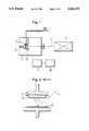
- FIG. 2is a schematic diagram illustrating a manufacturing method for a high-temperature superconductive oxide thin film by means of laser.
- a laser beam 1 oscillated from a laser devicesuch as a YAG laser device or an ArF excimer laser device is obliquely irradiated onto a target 2 provided with an oxide for formation of a thin film to cut the bond of particles constituting the target and simultaneously excite the particles to a high energy state.
- a luminous region called a plume consisting of active evaporated particlesis formed, and when the plume reaches a substrate 3 heated by a heater 4 or the like, a high-temperature superconductive thin film is obtained.
- an oxygen partial pressure during film formationis made high from the viewpoint of improvement in Tc end of a superconductive oxide thin film.
- the oxygen partial pressure during film formationis high, the plume is reduced in shape, resulting in a low probability of reaching of the active particles to the substrate.
- a distance between the target and the substrateis reduced to allow the plume to easily reach the substrate.
- this methodcannot be adopted because it is necessary to define a given distance between the target and the substrate so as to irradiate the laser beam onto the target.
- the oxygen partial pressureis reduced during film formation, and after forming the thin film, a post-treatment is carried out such as by cooling and maintaining the thin film in the atmosphere of oxygen to incorporate oxygen particles into the thin film, thereby improving Tc end.
- the present inventionhas been accomplished in view of the above circumstances, and it provides a manufacturing method for a high-temperature superconductive oxide thin film wherein the superconductive oxide thin film is formed under a high oxygen partial pressure to obtain a high Tc end without a post-treatment of cooling and maintaining the thin film in the atmosphere of oxygen, and no noise is generated in the case that the superconductive oxide thin film is practically applied to a superconductive device.
- FIG. 1is a schematic diagram illustrating a film forming method according to a preferred embodiment of the present invention
- FIG. 2is a schematic diagram illustrating a film forming method in the prior art
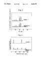
- FIGS. 3 and 4are graphs illustrating the results of X-ray diffraction according to the preferred embodiment in comparison with the prior art
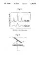
- FIG. 5is a graph illustrating the result of electron beam diffraction of a substrate before and after laser irradiation
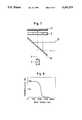
- FIGS. 6 and 7are schematic diagrams illustrating film forming methods according to other preferred embodiments of the present invention.
- FIG. 8is a graph illustrating a characteristic of a multi-layer film mirror employable in the present invention.
- FIG. 1shows a typical example of a device to be preferably used in performing the manufacturing method according to the present invention.
- a target 2 having a predetermined oxide compositionis retained by a target holder 5 movable in vertical and horizontal directions and rotatable.
- a substrate 3is so provided as to face the target 2, and it is fixed by a substrate holder 6.
- a laser device 7is provided on a normal with respect to a back surface of the substrate 3.
- a laser beam 1is irradiated from the side of the back surface of the substrate 3 and is transmitted through the substrate 3.
- the transmitted laser beam 1is irradiated onto the target 2 to deposit an oxide of the target 2 onto the substrate 3, thus forming a thin film of the oxide.
- the substrate 3may be made of an oxide capable of transmitting a laser beam.
- an oxidecapable of transmitting a laser beam.
- examples of such an oxidemay include MgO, SrTiO 3 , LaAlO 3 , LiNbO 3 , LaGaO 3 , quartz glass, and sapphire.
- the oxide targetmay be suitably selected according to a high-temperature superconductive oxide thin film to be manufactured.
- a superconductive thin film of Y oxideRBa 2 Cu 3 O 7- ⁇ (R: Y or La series elements) may be used.
- a superconductor of Bi or Tl oxidemay be used as the oxide target.
- the targetcan be sufficiently approached to the substrate during film formation. Accordingly, even in the atmosphere of oxygen under an oxygen partial pressure remarkably higher than that in the prior art, the thin film can be formed under the condition that the plume can easily reach the substrate.
- the superconductive thin filmcan sufficiently incorporate oxygen in a crystal structure. Further, since no twin plane is formed, it is possible to manufacture a thin film having a high Tc end and a high Jc and reducing a magnetic flux trap in the case that the thin film is applied to a superconductive device.
- the oxygen partial pressureis set to preferably 10 mTorr-760 Torr. If it is less than 10 mTorr, the Tc improving effect does not sufficiently appear, while if it is more than 760 Torr, the film is undesirably deposited like powder. More preferably, the range of the oxygen partial pressure is set to 100 mTorr-100 Torr.
- a laser absorbing filmis formed on a subject surface or a back surface of the substrate, so that the substrate is heated by the laser beam while it is being transmitted through the substrate. At the same time the irradiation of the laser beam is ended, the substrate is rapidly cooled.
- a film thickness of the laser absorbing filmis set to preferably 0.1-10 ⁇ m. If the film thickness is too small, laser absorption is insufficient, and the temperature of the substrate is not raised. If the film thickness is too large, a crystal property is deteriorated to undesirably cause separation of the film.
- an infrared raymay be irradiated to heat the substrate. If it is difficult to identify an irradiating direction of the laser beam with that of the infrared ray because of the magnitudes of a laser source and an infrared light source, it is recommended that a multi-layer film mirror 10 capable of transmitting the laser beam 1 and reflecting the infrared ray 13 is employed and located as shown in FIG. 7, so that the laser beam and the infrared ray can be irradiated onto the substrate in the same direction.
- the thin filmcan be formed at high speeds greater by three orders than the speed in the prior art, and the target material can be formed into the thin film on the substrate with a high probability to improve a deposition efficiency.
- the subject surface of the substratecan be cleaned by a photochemical reaction.
- the post-treatment after film formationis not necessary, a manufacturing time can be widely reduced, and the oxygen to be used in the post-treatment can be saved.
- a superconductive thin film of Y oxidewas formed under the test conditions shown in Table 1.
- the oxide targetYBa 2 Cu 3 O 7- ⁇ was used.
- the measurement results of a film thickness, Tc end and Jc at a practical temperature of 77Kare shown in Table 1.
- Example 1As a comparison, using a laser device similar to that used in Example 1, a thin film was formed by the conventional typical method as shown in FIG. 2. The test conditions and the evaluation results in the comparison are also shown in Table 1.
- the thin filmcan be formed at a high speed greater by three orders than that in Comparison. Moreover, Tc end in Example 1 is equal to that in Comparison, and Jc in Example 1 is higher than that in Comparison.
- the high film forming speedmeans that the film thickness per pulse is large, and it is understood that a utilization efficiency of the target can be improved.
- FIG. 3shows the result of X-ray diffraction of the films obtained in Example 1 and Comparison. It is understood that the crystal is well oriented in the direction of the C-axis in both Example 1 and Comparison.
- Example 1The reason why no twin plane is formed in Example 1 may be explained in the following manner. That is, since the film is formed under the very high oxygen partial pressure, the crystal structure becomes an orthorhombic system during the film formation. Furthermore, after the laser pulse is transmitted through the substrate, the substrate is naturally rapidly cooled. Therefore, it is considered that the oxygen in the film does not come out and no strain is accordingly generated in the crystal structure.
- the subject surface of the substrateis cleaned by a photochemical reaction upon transmitting of the laser beam through the substrate.
- the laser beamwas transmitted through the substrate of MgO (100) without being irradiated onto the target under the conditions of vacuum of 10 -7 Torr, laser irradiation power density of 3.0 J/cm 2 and laser pulse number of 1.
- the states of the subject surface of the substrate before and after the irradiation of the laser beamwere observed and compared with each other by using RHEED (reflection high-energy electron diffraction). The result is shown in FIG. 5.
- Example 3Jc was 3 ⁇ 10 5 A/cm 2 , and all of the film thickness, the film forming speed and Tc end were similar to those in Example 1.
- the thin film obtainedwas a polycrystal rather than a single crystal, it may be formed into a microbridge, which may be applied to an electromagnetic wave sensor by utilizing a weak bond between the superconductive crystals.
- the film formationwas carried out by irradiating the laser beam 1 of 10 pulses in the same manner as that in Example 1 with the exception that the target 2 was inclined to the substrate 3 at a predetermined angle ⁇ as shown in FIG. 6.
- the characteristics of the thin film formedwere evaluated to obtain the results similar to those in Example 1.
- the thin filmis not formed at a laser transmitted portion on the subject surface of the substrate. Accordingly, the laser beam can be continuously irradiated, so that the thin film can be formed in a wide range by moving the substrate.
- the film formationwas carried out in the same manner as that in Example 1 with the exception that a laser absorbing film was not formed on the substrate 3, but a multi-layer film mirror 10 was located between the substrate 3, and the laser device 7 as shown in FIG. 7. That is, an infrared ray 13 having a wavelength of 2700 nm was reflected on the multi-layer film mirror 10 to heat the substrate 3.
- the characteristics of the thin film formedwere evaluated to obtain the results similar to those in Example 1.
- the multi-layer film mirror 10is capable of transmitting a laser beam (355 nm) and reflecting an infrared ray (2700 nm), and it has a characteristic shown in FIG. 8.
- the film formationwas carried out in the same manner as the above, and the characteristics of the thin film formed were evaluated to obtain the results similar to those in Example 1.
- the present inventionit is not necessary to perform a post-treatment of cooling and maintaining a thin film in the atmosphere of oxygen after film formation.
- the subject surface of the substrateis cleaned during the film formation, and the high-temperature superconductive oxide thin film can be manufactured at high speeds.
Landscapes
- Chemical & Material Sciences (AREA)
- Engineering & Computer Science (AREA)
- Ceramic Engineering (AREA)
- Materials Engineering (AREA)
- Organic Chemistry (AREA)
- Structural Engineering (AREA)
- Inorganic Chemistry (AREA)
- Chemical Kinetics & Catalysis (AREA)
- Mechanical Engineering (AREA)
- Metallurgy (AREA)
- Health & Medical Sciences (AREA)
- Toxicology (AREA)
- Physics & Mathematics (AREA)
- Optics & Photonics (AREA)
- Manufacturing & Machinery (AREA)
- Superconductor Devices And Manufacturing Methods Thereof (AREA)
- Superconductors And Manufacturing Methods Therefor (AREA)
- Physical Vapour Deposition (AREA)
- Oxygen, Ozone, And Oxides In General (AREA)
- Inorganic Compounds Of Heavy Metals (AREA)
- Crystals, And After-Treatments Of Crystals (AREA)
Abstract
Description
TABLE 1 ______________________________________ Example 1 Comparison ______________________________________ (Test Conditions) Substrate MgO (100) MgO (100) (*) Heating of Substrate (**1) (**2) Oxygen Partial 10 0.1 Pressure (Torr) Target-Substrate 3 50 Distance (mm)Laser Shot Number 1 1 × 10.sup.3Laser Enery 3 3 Density (J/cm.sup.2) Cooling Method (***1) (***2) (Evaluation Results) Film Thickness (Å) 300 300 Film Forming 300 0.3 Speed (Å/shot) Tc end (K) 90 90 Jc (A/cm.sup.2) 3 × 10.sup.6 2.5 × 10.sup.6 ______________________________________ *: SrTiO.sub.3 film of 5 μm thick is formed as a laser absorbing film. **1: heating by laser irradiation **2: heating by heater at 700° C. ***1: natural rapid cooling after heating by laser irradiation ***2: gradual cooling in the atmosphere of oxygen additionally added unde 300 Torr
Claims (6)
Applications Claiming Priority (2)
| Application Number | Priority Date | Filing Date | Title |
|---|---|---|---|
| JP2-220466 | 1990-08-21 | ||
| JP2220466AJPH04104903A (en) | 1990-08-21 | 1990-08-21 | Production oxide high-temperature superconducting thin film |
Publications (1)
| Publication Number | Publication Date |
|---|---|
| US5281575Atrue US5281575A (en) | 1994-01-25 |
Family
ID=16751562
Family Applications (1)
| Application Number | Title | Priority Date | Filing Date |
|---|---|---|---|
| US07/848,004Expired - Fee RelatedUS5281575A (en) | 1990-08-21 | 1991-08-15 | Laser ablation method for forming oxide superconducting films |
Country Status (5)
| Country | Link |
|---|---|
| US (1) | US5281575A (en) |
| EP (1) | EP0496897B1 (en) |
| JP (1) | JPH04104903A (en) |
| DE (1) | DE69118676T2 (en) |
| WO (1) | WO1992003376A1 (en) |
Cited By (8)
| Publication number | Priority date | Publication date | Assignee | Title |
|---|---|---|---|---|
| US5612099A (en)* | 1995-05-23 | 1997-03-18 | Mcdonnell Douglas Corporation | Method and apparatus for coating a substrate |
| US5814152A (en)* | 1995-05-23 | 1998-09-29 | Mcdonnell Douglas Corporation | Apparatus for coating a substrate |
| US6440503B1 (en) | 2000-02-25 | 2002-08-27 | Scimed Life Systems, Inc. | Laser deposition of elements onto medical devices |
| US6451391B1 (en)* | 1998-09-10 | 2002-09-17 | Matsushita Electric Industrial Co., Ltd. | Thin film formation method |
| US6650464B2 (en)* | 2001-01-25 | 2003-11-18 | Sharp Kabushiki Kaisha | Laser processing device and organic electroluminescent display panel using the same |
| US6709720B2 (en) | 1997-03-21 | 2004-03-23 | Kabushiki Kaisha Yaskawa Denki | Marking method and marking material |
| US20060141136A1 (en)* | 2001-09-14 | 2006-06-29 | Seiko Epson Corporation | System and methods for manufacturing an organic electroluminescent element |
| US20100000466A1 (en)* | 2006-04-17 | 2010-01-07 | Imra America, Inc. | P-Type Semiconductor Zinc Oxide Films Process for Preparation Thereof, and Pulsed Laser Deposition Method Using Transparent Substrates |
Families Citing this family (3)
| Publication number | Priority date | Publication date | Assignee | Title |
|---|---|---|---|---|
| JP5327932B2 (en)* | 2007-02-08 | 2013-10-30 | 独立行政法人産業技術総合研究所 | Manufacturing method of superconducting coating material |
| JP5201518B2 (en)* | 2009-05-26 | 2013-06-05 | 株式会社日本製鋼所 | Method and apparatus for manufacturing superconducting oxide material |
| JP2012084430A (en)* | 2010-10-13 | 2012-04-26 | Fujikura Ltd | Oxide superconductor manufacturing method |
Citations (8)
| Publication number | Priority date | Publication date | Assignee | Title |
|---|---|---|---|---|
| US4743463A (en)* | 1986-02-21 | 1988-05-10 | Eastman Kodak Company | Method for forming patterns on a substrate or support |
| JPH01179473A (en)* | 1988-01-06 | 1989-07-17 | Semiconductor Energy Lab Co Ltd | Film formation method using light |
| JPH0217685A (en)* | 1988-05-11 | 1990-01-22 | Siemens Ag | Method for manufacturing metal oxide superconducting material layer by laser evaporation |
| JPH0288409A (en)* | 1988-07-03 | 1990-03-28 | Kernforschungsanlage Juelich Gmbh | Method for manufacturing thin layers of oxide-based high temperature superconductors |
| JPH02197565A (en)* | 1989-01-25 | 1990-08-06 | Fujikura Ltd | Target for laser evaporation equipment |
| JPH02250222A (en)* | 1989-02-13 | 1990-10-08 | Hitachi Ltd | Thin film formation method |
| US4970196A (en)* | 1987-01-15 | 1990-11-13 | The Johns Hopkins University | Method and apparatus for the thin film deposition of materials with a high power pulsed laser |
| US4987006A (en)* | 1990-03-26 | 1991-01-22 | Amp Incorporated | Laser transfer deposition |
Family Cites Families (1)
| Publication number | Priority date | Publication date | Assignee | Title |
|---|---|---|---|---|
| CA1105093A (en)* | 1977-12-21 | 1981-07-14 | Roland F. Drew | Laser deposition of metal upon transparent materials |
- 1990
- 1990-08-21JPJP2220466Apatent/JPH04104903A/enactivePending
- 1991
- 1991-08-15DEDE69118676Tpatent/DE69118676T2/ennot_activeExpired - Fee Related
- 1991-08-15WOPCT/JP1991/001086patent/WO1992003376A1/enactiveIP Right Grant
- 1991-08-15EPEP91914630Apatent/EP0496897B1/ennot_activeExpired - Lifetime
- 1991-08-15USUS07/848,004patent/US5281575A/ennot_activeExpired - Fee Related
Patent Citations (8)
| Publication number | Priority date | Publication date | Assignee | Title |
|---|---|---|---|---|
| US4743463A (en)* | 1986-02-21 | 1988-05-10 | Eastman Kodak Company | Method for forming patterns on a substrate or support |
| US4970196A (en)* | 1987-01-15 | 1990-11-13 | The Johns Hopkins University | Method and apparatus for the thin film deposition of materials with a high power pulsed laser |
| JPH01179473A (en)* | 1988-01-06 | 1989-07-17 | Semiconductor Energy Lab Co Ltd | Film formation method using light |
| JPH0217685A (en)* | 1988-05-11 | 1990-01-22 | Siemens Ag | Method for manufacturing metal oxide superconducting material layer by laser evaporation |
| JPH0288409A (en)* | 1988-07-03 | 1990-03-28 | Kernforschungsanlage Juelich Gmbh | Method for manufacturing thin layers of oxide-based high temperature superconductors |
| JPH02197565A (en)* | 1989-01-25 | 1990-08-06 | Fujikura Ltd | Target for laser evaporation equipment |
| JPH02250222A (en)* | 1989-02-13 | 1990-10-08 | Hitachi Ltd | Thin film formation method |
| US4987006A (en)* | 1990-03-26 | 1991-01-22 | Amp Incorporated | Laser transfer deposition |
Non-Patent Citations (4)
| Title |
|---|
| Journal of Applied Physics, vol. 66, No. 1, Jul. 1, 1989, pp. 457 459, E. Fogarassy, et al., Laser Induced Forward Transfer of High Tc YBaCuO and BiSrCaCuO Superconducting Thin Films .* |
| Journal of Applied Physics, vol. 66, No. 1, Jul. 1, 1989, pp. 457-459, E. Fogarassy, et al., "Laser-Induced Forward Transfer of High-Tc YBaCuO and BiSrCaCuO Superconducting Thin Films". |
| Koren et al, "Highly oriented as deposited superconducting laser ablated thin films of YiBa2 Cu3 O7-8 on SrTiO3, zirconia, and Si substrates", Appl. Phys. Lett. 53(23) Dec. 1988, pp. 2330-2332. |
| Koren et al, Highly oriented as deposited superconducting laser ablated thin films of YiBa 2 Cu 3 O 7 8 on SrTiO 3 , zirconia, and S i substrates , Appl. Phys. Lett. 53(23) Dec. 1988, pp. 2330 2332.* |
Cited By (11)
| Publication number | Priority date | Publication date | Assignee | Title |
|---|---|---|---|---|
| US5612099A (en)* | 1995-05-23 | 1997-03-18 | Mcdonnell Douglas Corporation | Method and apparatus for coating a substrate |
| US5814152A (en)* | 1995-05-23 | 1998-09-29 | Mcdonnell Douglas Corporation | Apparatus for coating a substrate |
| US6709720B2 (en) | 1997-03-21 | 2004-03-23 | Kabushiki Kaisha Yaskawa Denki | Marking method and marking material |
| US6451391B1 (en)* | 1998-09-10 | 2002-09-17 | Matsushita Electric Industrial Co., Ltd. | Thin film formation method |
| US20020197493A1 (en)* | 1998-09-10 | 2002-12-26 | Matsushita Electric Industrial Co., Ltd. | Thin film formation method, and functional material and applied device there with background of the invention |
| US6440503B1 (en) | 2000-02-25 | 2002-08-27 | Scimed Life Systems, Inc. | Laser deposition of elements onto medical devices |
| US6723390B2 (en) | 2000-02-25 | 2004-04-20 | Scimed Life Systems, Inc. | Laser deposition of elements onto medical devices |
| US6650464B2 (en)* | 2001-01-25 | 2003-11-18 | Sharp Kabushiki Kaisha | Laser processing device and organic electroluminescent display panel using the same |
| US20060141136A1 (en)* | 2001-09-14 | 2006-06-29 | Seiko Epson Corporation | System and methods for manufacturing an organic electroluminescent element |
| US20100000466A1 (en)* | 2006-04-17 | 2010-01-07 | Imra America, Inc. | P-Type Semiconductor Zinc Oxide Films Process for Preparation Thereof, and Pulsed Laser Deposition Method Using Transparent Substrates |
| CN101942642A (en)* | 2006-04-17 | 2011-01-12 | Imra美国公司 | P-type semiconductor zinc oxide film, method for preparing the same, and pulsed laser deposition method using transparent substrate |
Also Published As
| Publication number | Publication date |
|---|---|
| WO1992003376A1 (en) | 1992-03-05 |
| JPH04104903A (en) | 1992-04-07 |
| EP0496897A1 (en) | 1992-08-05 |
| DE69118676T2 (en) | 1996-10-02 |
| EP0496897B1 (en) | 1996-04-10 |
| EP0496897A4 (en) | 1993-04-14 |
| DE69118676D1 (en) | 1996-05-15 |
Similar Documents
| Publication | Publication Date | Title |
|---|---|---|
| CN110344008B (en) | Pulse laser coating device | |
| JP2660248B2 (en) | Film formation method using light | |
| JP2757284B2 (en) | Method for producing metal oxide superconducting material layer by laser evaporation | |
| US5281575A (en) | Laser ablation method for forming oxide superconducting films | |
| CN108277461B (en) | Antifouling device suitable for pulse laser coating and pulse laser coating device thereof | |
| CN108220888B (en) | Heating device suitable for pulse laser coating and pulse laser coating device thereof | |
| Bäuerle | Laser-induced formation and surface processing of high-temperature superconductors | |
| CN108277457B (en) | Light path device suitable for pulse laser coating and pulse laser coating device thereof | |
| JPH0297427A (en) | Production of oxide superconducting thin film | |
| US5527767A (en) | Method for annealing thin film superconductors | |
| JP3465041B2 (en) | YAG fifth harmonic pulse laser vapor deposition method and apparatus | |
| EP0392437B1 (en) | Method for annealing thin film superconductors | |
| US5234901A (en) | Process for depositing a different thin film on an oxide superconductor | |
| JP2002068889A (en) | Method for producing (0001) epitaxial thin film of hexagonal substance such as zinc oxide using cubic oxide (111) substrate and thin film produced by the same method | |
| JPH02271905A (en) | Method for annealing oxide superconducting thin film | |
| JP2810930B2 (en) | Film forming method using laser light | |
| Kita et al. | Epitaxial growth of BaO and SrO with new crystal structures using mass-separated low-energy O+ beams | |
| US5250511A (en) | Laser evaporation method for preparing a superconducting oxide thin film | |
| JP2813691B2 (en) | Laser deposition target | |
| JP3522402B2 (en) | Method and apparatus for producing oxide superconducting conductor | |
| JPH02120229A (en) | Production of superconducting thin film of oxide | |
| JPH01215963A (en) | Superconducting thin film formation method | |
| JPH0781934A (en) | Superconductor and production thereof | |
| Kawaiw et al. | Formation and processing of high Tc superconductor films with pulsed excimer laser | |
| JPH07206436A (en) | Superconductor and its production |
Legal Events
| Date | Code | Title | Description |
|---|---|---|---|
| AS | Assignment | Owner name:HITACHI DENSEN KABUSHIKI KAISHA, JAPAN Free format text:ASSIGNMENT OF ASSIGNORS INTEREST.;ASSIGNORS:HASE, TAKASHI;MORISHITA, TADATAKA;OHATA, KATSUMI;AND OTHERS;REEL/FRAME:006486/0923;SIGNING DATES FROM 19920325 TO 19920407 Owner name:KABUSHIKI KAISHA KOBE SEIKO SHO, JAPAN Free format text:ASSIGNMENT OF ASSIGNORS INTEREST.;ASSIGNORS:HASE, TAKASHI;MORISHITA, TADATAKA;OHATA, KATSUMI;AND OTHERS;REEL/FRAME:006486/0923;SIGNING DATES FROM 19920325 TO 19920407 Owner name:INTERNATIONAL SUPERCONDUCTIVITY TECHNOLOGY CENTER, Free format text:ASSIGNMENT OF ASSIGNORS INTEREST.;ASSIGNORS:HASE, TAKASHI;MORISHITA, TADATAKA;OHATA, KATSUMI;AND OTHERS;REEL/FRAME:006486/0923;SIGNING DATES FROM 19920325 TO 19920407 | |
| FPAY | Fee payment | Year of fee payment:4 | |
| FEPP | Fee payment procedure | Free format text:PAYOR NUMBER ASSIGNED (ORIGINAL EVENT CODE: ASPN); ENTITY STATUS OF PATENT OWNER: LARGE ENTITY | |
| FPAY | Fee payment | Year of fee payment:8 | |
| AS | Assignment | Owner name:HITACHI DENSEN KABUSHIKI KAISHA, JAPAN Free format text:CORPORATE ADDRESS CHANGE;ASSIGNOR:HITACHI DENSEN KABUSHIKI KAISHA;REEL/FRAME:014653/0569 Effective date:19991122 Owner name:KABUSHIKI KAISHA KOBE SEIKO SHO, JAPAN Free format text:CORPORATE ADDRESS CHANGE;ASSIGNOR:KABUSHIKI KAISHA KOBE SEIKO SHO;REEL/FRAME:014653/0587 Effective date:20020301 | |
| AS | Assignment | Owner name:NEW ENERGY AND INDUSTRIAL TECHNOLOGY DEPARTMENT OR Free format text:ASSIGNMENT OF ASSIGNORS INTEREST;ASSIGNORS:INTERNATIONAL SUPERCONDUCTIVITY TECHNOLOGY CENTER;KABUSHIKI KAISHA KOBE SEIKO SHO;HITACHI DENSEN KABUSHIKI KAISHA;REEL/FRAME:015139/0240;SIGNING DATES FROM 20040826 TO 20040907 | |
| REMI | Maintenance fee reminder mailed | ||
| LAPS | Lapse for failure to pay maintenance fees | ||
| STCH | Information on status: patent discontinuation | Free format text:PATENT EXPIRED DUE TO NONPAYMENT OF MAINTENANCE FEES UNDER 37 CFR 1.362 | |
| FP | Lapsed due to failure to pay maintenance fee | Effective date:20060125 |