US5280193A - Repairable semiconductor multi-package module having individualized package bodies on a PC board substrate - Google Patents
Repairable semiconductor multi-package module having individualized package bodies on a PC board substrateDownload PDFInfo
- Publication number
- US5280193A US5280193AUS07/877,930US87793092AUS5280193AUS 5280193 AUS5280193 AUS 5280193AUS 87793092 AUS87793092 AUS 87793092AUS 5280193 AUS5280193 AUS 5280193A
- Authority
- US
- United States
- Prior art keywords
- material substrate
- board material
- semiconductor
- package
- conductive paths
- Prior art date
- Legal status (The legal status is an assumption and is not a legal conclusion. Google has not performed a legal analysis and makes no representation as to the accuracy of the status listed.)
- Expired - Lifetime
Links
Images
Classifications
- H—ELECTRICITY
- H01—ELECTRIC ELEMENTS
- H01L—SEMICONDUCTOR DEVICES NOT COVERED BY CLASS H10
- H01L21/00—Processes or apparatus adapted for the manufacture or treatment of semiconductor or solid state devices or of parts thereof
- H01L21/02—Manufacture or treatment of semiconductor devices or of parts thereof
- H01L21/04—Manufacture or treatment of semiconductor devices or of parts thereof the devices having potential barriers, e.g. a PN junction, depletion layer or carrier concentration layer
- H01L21/50—Assembly of semiconductor devices using processes or apparatus not provided for in a single one of the groups H01L21/18 - H01L21/326 or H10D48/04 - H10D48/07 e.g. sealing of a cap to a base of a container
- H01L21/56—Encapsulations, e.g. encapsulation layers, coatings
- H01L21/565—Moulds
- H—ELECTRICITY
- H01—ELECTRIC ELEMENTS
- H01L—SEMICONDUCTOR DEVICES NOT COVERED BY CLASS H10
- H01L23/00—Details of semiconductor or other solid state devices
- H01L23/28—Encapsulations, e.g. encapsulating layers, coatings, e.g. for protection
- H01L23/31—Encapsulations, e.g. encapsulating layers, coatings, e.g. for protection characterised by the arrangement or shape
- H01L23/3107—Encapsulations, e.g. encapsulating layers, coatings, e.g. for protection characterised by the arrangement or shape the device being completely enclosed
- H01L23/3121—Encapsulations, e.g. encapsulating layers, coatings, e.g. for protection characterised by the arrangement or shape the device being completely enclosed a substrate forming part of the encapsulation
- H—ELECTRICITY
- H01—ELECTRIC ELEMENTS
- H01L—SEMICONDUCTOR DEVICES NOT COVERED BY CLASS H10
- H01L24/00—Arrangements for connecting or disconnecting semiconductor or solid-state bodies; Methods or apparatus related thereto
- H01L24/93—Batch processes
- H01L24/95—Batch processes at chip-level, i.e. with connecting carried out on a plurality of singulated devices, i.e. on diced chips
- H01L24/97—Batch processes at chip-level, i.e. with connecting carried out on a plurality of singulated devices, i.e. on diced chips the devices being connected to a common substrate, e.g. interposer, said common substrate being separable into individual assemblies after connecting
- H—ELECTRICITY
- H01—ELECTRIC ELEMENTS
- H01L—SEMICONDUCTOR DEVICES NOT COVERED BY CLASS H10
- H01L2224/00—Indexing scheme for arrangements for connecting or disconnecting semiconductor or solid-state bodies and methods related thereto as covered by H01L24/00
- H01L2224/01—Means for bonding being attached to, or being formed on, the surface to be connected, e.g. chip-to-package, die-attach, "first-level" interconnects; Manufacturing methods related thereto
- H01L2224/26—Layer connectors, e.g. plate connectors, solder or adhesive layers; Manufacturing methods related thereto
- H01L2224/31—Structure, shape, material or disposition of the layer connectors after the connecting process
- H01L2224/32—Structure, shape, material or disposition of the layer connectors after the connecting process of an individual layer connector
- H01L2224/321—Disposition
- H01L2224/32151—Disposition the layer connector connecting between a semiconductor or solid-state body and an item not being a semiconductor or solid-state body, e.g. chip-to-substrate, chip-to-passive
- H01L2224/32221—Disposition the layer connector connecting between a semiconductor or solid-state body and an item not being a semiconductor or solid-state body, e.g. chip-to-substrate, chip-to-passive the body and the item being stacked
- H01L2224/32225—Disposition the layer connector connecting between a semiconductor or solid-state body and an item not being a semiconductor or solid-state body, e.g. chip-to-substrate, chip-to-passive the body and the item being stacked the item being non-metallic, e.g. insulating substrate with or without metallisation
- H—ELECTRICITY
- H01—ELECTRIC ELEMENTS
- H01L—SEMICONDUCTOR DEVICES NOT COVERED BY CLASS H10
- H01L2224/00—Indexing scheme for arrangements for connecting or disconnecting semiconductor or solid-state bodies and methods related thereto as covered by H01L24/00
- H01L2224/01—Means for bonding being attached to, or being formed on, the surface to be connected, e.g. chip-to-package, die-attach, "first-level" interconnects; Manufacturing methods related thereto
- H01L2224/42—Wire connectors; Manufacturing methods related thereto
- H01L2224/44—Structure, shape, material or disposition of the wire connectors prior to the connecting process
- H01L2224/45—Structure, shape, material or disposition of the wire connectors prior to the connecting process of an individual wire connector
- H01L2224/45001—Core members of the connector
- H01L2224/45099—Material
- H01L2224/451—Material with a principal constituent of the material being a metal or a metalloid, e.g. boron (B), silicon (Si), germanium (Ge), arsenic (As), antimony (Sb), tellurium (Te) and polonium (Po), and alloys thereof
- H01L2224/45117—Material with a principal constituent of the material being a metal or a metalloid, e.g. boron (B), silicon (Si), germanium (Ge), arsenic (As), antimony (Sb), tellurium (Te) and polonium (Po), and alloys thereof the principal constituent melting at a temperature of greater than or equal to 400°C and less than 950°C
- H01L2224/45124—Aluminium (Al) as principal constituent
- H—ELECTRICITY
- H01—ELECTRIC ELEMENTS
- H01L—SEMICONDUCTOR DEVICES NOT COVERED BY CLASS H10
- H01L2224/00—Indexing scheme for arrangements for connecting or disconnecting semiconductor or solid-state bodies and methods related thereto as covered by H01L24/00
- H01L2224/01—Means for bonding being attached to, or being formed on, the surface to be connected, e.g. chip-to-package, die-attach, "first-level" interconnects; Manufacturing methods related thereto
- H01L2224/42—Wire connectors; Manufacturing methods related thereto
- H01L2224/44—Structure, shape, material or disposition of the wire connectors prior to the connecting process
- H01L2224/45—Structure, shape, material or disposition of the wire connectors prior to the connecting process of an individual wire connector
- H01L2224/45001—Core members of the connector
- H01L2224/45099—Material
- H01L2224/451—Material with a principal constituent of the material being a metal or a metalloid, e.g. boron (B), silicon (Si), germanium (Ge), arsenic (As), antimony (Sb), tellurium (Te) and polonium (Po), and alloys thereof
- H01L2224/45138—Material with a principal constituent of the material being a metal or a metalloid, e.g. boron (B), silicon (Si), germanium (Ge), arsenic (As), antimony (Sb), tellurium (Te) and polonium (Po), and alloys thereof the principal constituent melting at a temperature of greater than or equal to 950°C and less than 1550°C
- H01L2224/45144—Gold (Au) as principal constituent
- H—ELECTRICITY
- H01—ELECTRIC ELEMENTS
- H01L—SEMICONDUCTOR DEVICES NOT COVERED BY CLASS H10
- H01L2224/00—Indexing scheme for arrangements for connecting or disconnecting semiconductor or solid-state bodies and methods related thereto as covered by H01L24/00
- H01L2224/01—Means for bonding being attached to, or being formed on, the surface to be connected, e.g. chip-to-package, die-attach, "first-level" interconnects; Manufacturing methods related thereto
- H01L2224/42—Wire connectors; Manufacturing methods related thereto
- H01L2224/44—Structure, shape, material or disposition of the wire connectors prior to the connecting process
- H01L2224/45—Structure, shape, material or disposition of the wire connectors prior to the connecting process of an individual wire connector
- H01L2224/45001—Core members of the connector
- H01L2224/45099—Material
- H01L2224/451—Material with a principal constituent of the material being a metal or a metalloid, e.g. boron (B), silicon (Si), germanium (Ge), arsenic (As), antimony (Sb), tellurium (Te) and polonium (Po), and alloys thereof
- H01L2224/45138—Material with a principal constituent of the material being a metal or a metalloid, e.g. boron (B), silicon (Si), germanium (Ge), arsenic (As), antimony (Sb), tellurium (Te) and polonium (Po), and alloys thereof the principal constituent melting at a temperature of greater than or equal to 950°C and less than 1550°C
- H01L2224/45147—Copper (Cu) as principal constituent
- H—ELECTRICITY
- H01—ELECTRIC ELEMENTS
- H01L—SEMICONDUCTOR DEVICES NOT COVERED BY CLASS H10
- H01L2224/00—Indexing scheme for arrangements for connecting or disconnecting semiconductor or solid-state bodies and methods related thereto as covered by H01L24/00
- H01L2224/01—Means for bonding being attached to, or being formed on, the surface to be connected, e.g. chip-to-package, die-attach, "first-level" interconnects; Manufacturing methods related thereto
- H01L2224/42—Wire connectors; Manufacturing methods related thereto
- H01L2224/47—Structure, shape, material or disposition of the wire connectors after the connecting process
- H01L2224/48—Structure, shape, material or disposition of the wire connectors after the connecting process of an individual wire connector
- H01L2224/4805—Shape
- H01L2224/4809—Loop shape
- H01L2224/48091—Arched
- H—ELECTRICITY
- H01—ELECTRIC ELEMENTS
- H01L—SEMICONDUCTOR DEVICES NOT COVERED BY CLASS H10
- H01L2224/00—Indexing scheme for arrangements for connecting or disconnecting semiconductor or solid-state bodies and methods related thereto as covered by H01L24/00
- H01L2224/01—Means for bonding being attached to, or being formed on, the surface to be connected, e.g. chip-to-package, die-attach, "first-level" interconnects; Manufacturing methods related thereto
- H01L2224/42—Wire connectors; Manufacturing methods related thereto
- H01L2224/47—Structure, shape, material or disposition of the wire connectors after the connecting process
- H01L2224/48—Structure, shape, material or disposition of the wire connectors after the connecting process of an individual wire connector
- H01L2224/481—Disposition
- H01L2224/48151—Connecting between a semiconductor or solid-state body and an item not being a semiconductor or solid-state body, e.g. chip-to-substrate, chip-to-passive
- H01L2224/48221—Connecting between a semiconductor or solid-state body and an item not being a semiconductor or solid-state body, e.g. chip-to-substrate, chip-to-passive the body and the item being stacked
- H01L2224/48225—Connecting between a semiconductor or solid-state body and an item not being a semiconductor or solid-state body, e.g. chip-to-substrate, chip-to-passive the body and the item being stacked the item being non-metallic, e.g. insulating substrate with or without metallisation
- H01L2224/48227—Connecting between a semiconductor or solid-state body and an item not being a semiconductor or solid-state body, e.g. chip-to-substrate, chip-to-passive the body and the item being stacked the item being non-metallic, e.g. insulating substrate with or without metallisation connecting the wire to a bond pad of the item
- H—ELECTRICITY
- H01—ELECTRIC ELEMENTS
- H01L—SEMICONDUCTOR DEVICES NOT COVERED BY CLASS H10
- H01L2224/00—Indexing scheme for arrangements for connecting or disconnecting semiconductor or solid-state bodies and methods related thereto as covered by H01L24/00
- H01L2224/73—Means for bonding being of different types provided for in two or more of groups H01L2224/10, H01L2224/18, H01L2224/26, H01L2224/34, H01L2224/42, H01L2224/50, H01L2224/63, H01L2224/71
- H01L2224/732—Location after the connecting process
- H01L2224/73251—Location after the connecting process on different surfaces
- H01L2224/73265—Layer and wire connectors
- H—ELECTRICITY
- H01—ELECTRIC ELEMENTS
- H01L—SEMICONDUCTOR DEVICES NOT COVERED BY CLASS H10
- H01L2224/00—Indexing scheme for arrangements for connecting or disconnecting semiconductor or solid-state bodies and methods related thereto as covered by H01L24/00
- H01L2224/93—Batch processes
- H01L2224/95—Batch processes at chip-level, i.e. with connecting carried out on a plurality of singulated devices, i.e. on diced chips
- H01L2224/97—Batch processes at chip-level, i.e. with connecting carried out on a plurality of singulated devices, i.e. on diced chips the devices being connected to a common substrate, e.g. interposer, said common substrate being separable into individual assemblies after connecting
- H—ELECTRICITY
- H01—ELECTRIC ELEMENTS
- H01L—SEMICONDUCTOR DEVICES NOT COVERED BY CLASS H10
- H01L24/00—Arrangements for connecting or disconnecting semiconductor or solid-state bodies; Methods or apparatus related thereto
- H01L24/01—Means for bonding being attached to, or being formed on, the surface to be connected, e.g. chip-to-package, die-attach, "first-level" interconnects; Manufacturing methods related thereto
- H01L24/42—Wire connectors; Manufacturing methods related thereto
- H01L24/44—Structure, shape, material or disposition of the wire connectors prior to the connecting process
- H01L24/45—Structure, shape, material or disposition of the wire connectors prior to the connecting process of an individual wire connector
- H—ELECTRICITY
- H01—ELECTRIC ELEMENTS
- H01L—SEMICONDUCTOR DEVICES NOT COVERED BY CLASS H10
- H01L24/00—Arrangements for connecting or disconnecting semiconductor or solid-state bodies; Methods or apparatus related thereto
- H01L24/01—Means for bonding being attached to, or being formed on, the surface to be connected, e.g. chip-to-package, die-attach, "first-level" interconnects; Manufacturing methods related thereto
- H01L24/42—Wire connectors; Manufacturing methods related thereto
- H01L24/47—Structure, shape, material or disposition of the wire connectors after the connecting process
- H01L24/48—Structure, shape, material or disposition of the wire connectors after the connecting process of an individual wire connector
- H—ELECTRICITY
- H01—ELECTRIC ELEMENTS
- H01L—SEMICONDUCTOR DEVICES NOT COVERED BY CLASS H10
- H01L24/00—Arrangements for connecting or disconnecting semiconductor or solid-state bodies; Methods or apparatus related thereto
- H01L24/73—Means for bonding being of different types provided for in two or more of groups H01L24/10, H01L24/18, H01L24/26, H01L24/34, H01L24/42, H01L24/50, H01L24/63, H01L24/71
- H—ELECTRICITY
- H01—ELECTRIC ELEMENTS
- H01L—SEMICONDUCTOR DEVICES NOT COVERED BY CLASS H10
- H01L2924/00—Indexing scheme for arrangements or methods for connecting or disconnecting semiconductor or solid-state bodies as covered by H01L24/00
- H01L2924/0001—Technical content checked by a classifier
- H01L2924/00014—Technical content checked by a classifier the subject-matter covered by the group, the symbol of which is combined with the symbol of this group, being disclosed without further technical details
- H—ELECTRICITY
- H01—ELECTRIC ELEMENTS
- H01L—SEMICONDUCTOR DEVICES NOT COVERED BY CLASS H10
- H01L2924/00—Indexing scheme for arrangements or methods for connecting or disconnecting semiconductor or solid-state bodies as covered by H01L24/00
- H01L2924/01—Chemical elements
- H01L2924/01013—Aluminum [Al]
- H—ELECTRICITY
- H01—ELECTRIC ELEMENTS
- H01L—SEMICONDUCTOR DEVICES NOT COVERED BY CLASS H10
- H01L2924/00—Indexing scheme for arrangements or methods for connecting or disconnecting semiconductor or solid-state bodies as covered by H01L24/00
- H01L2924/01—Chemical elements
- H01L2924/01029—Copper [Cu]
- H—ELECTRICITY
- H01—ELECTRIC ELEMENTS
- H01L—SEMICONDUCTOR DEVICES NOT COVERED BY CLASS H10
- H01L2924/00—Indexing scheme for arrangements or methods for connecting or disconnecting semiconductor or solid-state bodies as covered by H01L24/00
- H01L2924/01—Chemical elements
- H01L2924/01033—Arsenic [As]
- H—ELECTRICITY
- H01—ELECTRIC ELEMENTS
- H01L—SEMICONDUCTOR DEVICES NOT COVERED BY CLASS H10
- H01L2924/00—Indexing scheme for arrangements or methods for connecting or disconnecting semiconductor or solid-state bodies as covered by H01L24/00
- H01L2924/01—Chemical elements
- H01L2924/01078—Platinum [Pt]
- H—ELECTRICITY
- H01—ELECTRIC ELEMENTS
- H01L—SEMICONDUCTOR DEVICES NOT COVERED BY CLASS H10
- H01L2924/00—Indexing scheme for arrangements or methods for connecting or disconnecting semiconductor or solid-state bodies as covered by H01L24/00
- H01L2924/01—Chemical elements
- H01L2924/01079—Gold [Au]
- H—ELECTRICITY
- H01—ELECTRIC ELEMENTS
- H01L—SEMICONDUCTOR DEVICES NOT COVERED BY CLASS H10
- H01L2924/00—Indexing scheme for arrangements or methods for connecting or disconnecting semiconductor or solid-state bodies as covered by H01L24/00
- H01L2924/01—Chemical elements
- H01L2924/01082—Lead [Pb]
- H—ELECTRICITY
- H01—ELECTRIC ELEMENTS
- H01L—SEMICONDUCTOR DEVICES NOT COVERED BY CLASS H10
- H01L2924/00—Indexing scheme for arrangements or methods for connecting or disconnecting semiconductor or solid-state bodies as covered by H01L24/00
- H01L2924/10—Details of semiconductor or other solid state devices to be connected
- H01L2924/11—Device type
- H01L2924/12—Passive devices, e.g. 2 terminal devices
- H01L2924/1204—Optical Diode
- H01L2924/12042—LASER
- H—ELECTRICITY
- H01—ELECTRIC ELEMENTS
- H01L—SEMICONDUCTOR DEVICES NOT COVERED BY CLASS H10
- H01L2924/00—Indexing scheme for arrangements or methods for connecting or disconnecting semiconductor or solid-state bodies as covered by H01L24/00
- H01L2924/15—Details of package parts other than the semiconductor or other solid state devices to be connected
- H01L2924/151—Die mounting substrate
- H01L2924/156—Material
- H01L2924/15786—Material with a principal constituent of the material being a non metallic, non metalloid inorganic material
- H01L2924/15787—Ceramics, e.g. crystalline carbides, nitrides or oxides
- H—ELECTRICITY
- H01—ELECTRIC ELEMENTS
- H01L—SEMICONDUCTOR DEVICES NOT COVERED BY CLASS H10
- H01L2924/00—Indexing scheme for arrangements or methods for connecting or disconnecting semiconductor or solid-state bodies as covered by H01L24/00
- H01L2924/15—Details of package parts other than the semiconductor or other solid state devices to be connected
- H01L2924/181—Encapsulation
- H—ELECTRICITY
- H05—ELECTRIC TECHNIQUES NOT OTHERWISE PROVIDED FOR
- H05K—PRINTED CIRCUITS; CASINGS OR CONSTRUCTIONAL DETAILS OF ELECTRIC APPARATUS; MANUFACTURE OF ASSEMBLAGES OF ELECTRICAL COMPONENTS
- H05K3/00—Apparatus or processes for manufacturing printed circuits
- H05K3/0097—Processing two or more printed circuits simultaneously, e.g. made from a common substrate, or temporarily stacked circuit boards
- H—ELECTRICITY
- H05—ELECTRIC TECHNIQUES NOT OTHERWISE PROVIDED FOR
- H05K—PRINTED CIRCUITS; CASINGS OR CONSTRUCTIONAL DETAILS OF ELECTRIC APPARATUS; MANUFACTURE OF ASSEMBLAGES OF ELECTRICAL COMPONENTS
- H05K3/00—Apparatus or processes for manufacturing printed circuits
- H05K3/40—Forming printed elements for providing electric connections to or between printed circuits
- H05K3/403—Edge contacts; Windows or holes in the substrate having plural connections on the walls thereof
Definitions
- the present inventionrelates to semiconductor multiple package modules in general, and more specifically to the connection of multiple semiconductor dice onto a printed circuit board material substrate in which the substrate functions both as a leadframe connection for the semiconductor dice and as a printed circuit board.
- PCprinted circuit
- a compact packaging technologyis needed when mounting area is limited dictating that circuit elements be closely spaced.
- a module consisting of a plurality of semiconductor devicesis used to densely dispose semiconductor devices and to obtain a small-sized electronic apparatus.
- PC boardshave typically been designed so that semiconductor devices in the form of packaged semiconductor dice are mounted thereon to make a final circuit. Mounting can be accomplished by a surface mount technique or by socketing. Interconnections among devices arrayed on PC boards are usually made by conductive traces formed by photolithography and etching processes.
- Burn-inis performed to screen out weak devices, and packaged devices rather than bare chips are normally burned-in. In a multiple chip module, the burn-in process should be performed at the packaged module level.
- the drawback in module level burn-inis that a percentage of die in the module will fail, and replacement with another good die has to be performed by a proper removing procedure. The replacement procedure may not always be cost effective or easy to effect.
- SIMM boards or memory cardsare circuit arrays which are typically byte multiples of memory chips arranged on a daughter PC board or comparable mounting arrangement.
- the SIMM board or memory cardis connected to a circuit control board by an edge connector.
- One edge of a SIMM moduleis a card edge connector, which plugs into a socket on the computer which is directly connected to the computer busses required for powering and addressing the memory on the SIMM.
- the semiconductor devices on SIMM boardsare typically packaged in small outline J-leaded packages (SOJs) or thin small outline packages (TSOPs) before they are mounted on the daughter PC board.
- SOJssmall outline J-leaded packages
- TSOPsthin small outline packages
- SIPsSingle in-line packages
- SIMMsSingle in-line packages
- pinswhich are either socket mounted or solder mounted to a mother board or bus.
- These moduleshave been constructed by first packaging individual semiconductor dice into packages, and then soldering the packaged dice onto a daughter PC board. These packages are attached to the daughter board by surface mount techniques or into through-holes.
- SIMMs and SIPSThe disadvantage to both SIMMs and SIPS is that the semiconductor dice have to be packaged individually before they are mounted on a daughter board. Furthermore, each device is tested and burned-in on a discrete unit level instead of a module level.
- a semiconductor moduleuses a cofired ceramic substrate, onto which bare semiconductor dice are directly attached to the ceramic mounting surface and are wire bonded to conductive areas on the mounting surface, or are inverted and connected directly to metallized areas on the ceramic mounting surface by, for example, a solder-bump technique.
- direct chip attachhas a limitation of no burn-in capability before module assembly and is difficult to repair after board mounting.
- Another method of fabricating a semiconductor moduleinvolves tape automated bonded (TAB) semiconductor dice to a flexible circuit leadframe, which also serves as a printed circuit board.
- TABtape automated bonded
- the semiconductor diceare tested as discrete units before being mounted, or they can be tested in the final circuit form after the TAB process.
- the flexible circuit leadframeis encapsulated.
- the dice and circuitry on the leadframe including the leadframeare encapsulated in a mold forming a single package body for the entire module.
- the disadvantage to this approachis that repair of the module after encapsulation is not possible. Hence, any failure of a semiconductor die inside the encapsulated module would cause the entire module to be rejected.
- a semiconductor multi-package modulehaving a first printed circuit (PC) board material substrate, a plurality of semiconductor dice, and an encapsulating material.
- the first PC board material substratehas a plurality of conductive paths including bonding pads and a plurality of edge connectors.
- the plurality of semiconductor diceare directly mounted to the first PC board material substrate, wherein the plurality of semiconductor dice are electrically interconnected by wire bonds to the bonding pads of the plurality of conductive paths.
- the encapsulating materialovermolds the plurality of semiconductor dice including the wire bonds on the first PC board material substrate, wherein the encapsulating material adheres to the PC board material substrate and forms an individualized package body for each of the plurality of semiconductor dice.
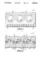
- FIG. 1is a top view of a multi-package module on a printed circuit (PC) board material substrate with edge connectors, according to a preferred embodiment of the present invention.
- PCprinted circuit
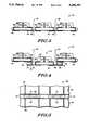
- FIG. 2is a cross-sectional view of a PC board material substrate having a plurality of semiconductor dice mounted and wire bonded thereon, the substrate assembly being inside a mold tool, in accordance with a method for making the multi-package module of FIG. 1.
- FIG. 3is a cross-sectional view of a multi-package module outlining a device replacement region for a non-functional semiconductor device, in accordance with a repair method of the invention.
- FIG. 4is a cross-sectional view of a multi-package module with a replacement semiconductor device, illustrating a method of repair in accordance with the invention.
- FIG. 5is a partial enlarged cross-sectional view of a jumper tape solder connection, illustrating a method of repairing the multi-package module in accordance with the invention.
- FIG. 1Illustrated in FIG. 1 is a top view of a finished semiconductor multi-package module 10 according to a preferred embodiment of the present invention, comprising a plurality of semiconductor devices 12, 14, and 16 directly mounted on a printed circuit (PC) board material substrate 18 having a plurality of edge connectors 20 for inserting into a socket (not shown).
- Semiconductor devices 12, 14, and 16are directly overmolded on the PC board material substrate 18 with a molding compound, for example, an epoxy resin-based molding compound.
- An overmolded semiconductor deviceis one where the encapsulating material or molding compound forms a package body only on one side of the supporting substrate for the semiconductor die.
- the PC board material substrate 18is of a standard construction.
- edge connectors 20are typically copper plated with solder or a metal alloy.
- PC board material substrate 18has circuit traces 22 with bonding pads enabling direct attachment and wire bonding of the semiconductor dice (not shown) inside each semiconductor device 12, 14, and 16 to substrate 18, wherein circuit traces 22 include a plurality of conductive paths (not fully shown) which connects the plurality of semiconductor devices 12, 14, and 16 to edge connectors 20 and to each other. Electrical interconnections between semiconductor devices can vary per the function of the semiconductor module, for example, a SIMM board or a memory card. Techniques for making these conductive paths and interconnections are well known in the art.
- FIG. 2a cross-section 30 of a PC board material substrate assembly 32 inside a mold tool 34 is illustrated.
- the PC board material substrate assembly 32comprises a PC board material substrate 36 having a plurality of circuit traces 38 extending to the backside of the substrate 36 and a plurality of semiconductor dice 40, 42, and 44 mounted on PC board material substrate 36 and wire bonded thereto with a plurality of wire bonds 46.
- Semiconductor dice 40, 42, and 44are directly mounted on PC board material substrate 36 and can be affixed thereto with a conventional die-attach epoxy.
- the semiconductor dice 40, 42, and 44are electrically connected to the PC board material substrate 36 with wire bonds 46.
- Wire bonds 46are of a conductive material such as gold, copper, aluminum, or alloys of these materials.
- the PC board material substrate 36has a plurality of through-hole vias 48. Additionally, the backside metallization 49 allows the method of repair to be effected.
- FIG. 2also illustrates a mold tool 34 having a plurality of die cavities 50 into which molding compound is injected to form package bodies.
- the semiconductor dice 40, 42, and 44 along with their respective wire bonds 46are overmolded in mold tool 34 wherein an individualized package body is formed for each semiconductor die. Overmolding can be done progressively for each semiconductor die, or it can be accomplished in one step, depending on the size of the mold tool and its design.
- the PC board material substrate 36is analogous to a leadframe in a conventional molding process because the leadframe is the supporting substrate for wire bonded semiconductor dice in a conventional molding process.
- the leadframeis placed inside a mold tool and individual package bodies are molded around each semiconductor die.
- the package bodyis substantially symmetrical around the leadframe and the semiconductor die.
- the package bodyis only formed on one side of the substrate.
- the finished productlooks substantially the same as the multi-package module 10 of FIG. 1.
- the semiconductor multi-package modulecan be tested and burned-in as a module. If all components of the module are functional, then the multi-package module can be shipped to the customer for his application.
- a method of repairing a faulty semiconductor multi-package moduleis provided. Illustrated in FIG. 3 is a cross-section of a semiconductor multi-package module 52, which is a post-molded version of the PC board material substrate assembly 32 of FIG. 2. Semiconductor dice 40, 42, and 44 are protected with a plurality of individual package bodies 54. Dotted lines 56 correspond to a device replacement region around any non-functional semiconductor device.
- the non-functional semiconductor deviceneeds to be removed from the module. The removal of the non-functioning device can be accomplished by either a mechanical method or by a laser scribing technique.
- semiconductor die 42is hypothetically non-functional, although it should be obvious that the following discussed method of repair is applicable to any non-functional semiconductor die of the multi-package module regardless of location on the PC board material substrate.
- FIG. 4Illustrated in FIG. 4 is a cross-sectional view of a repaired semiconductor multi-package module 60.
- the replacement section 62consists of a semiconductor die 42' with wire bonds 46' and an overmolded package body 54' directly mounted on a second PC board material substrate 36' having through-hole vias 48' and circuit traces 38'.
- Semiconductor die 42'performs the same functions as that of the removed non-functional die.
- Replacement section 62is essentially a punch-out from another semiconductor multi-package that has been manufactured using the method discussed previously. However, a replacement section having a semiconductor die that is encapsulated with a glob top instead of being overmolded with a molding compound can also be used for the repair of the module.
- replacement section 62is larger than device replacement region 56.
- the overlap of the first PC board material substrate 36 and the second PC board material substrate 36'allows the repair of the multi-package module to be effected.
- the backside metallization 49 of circuit traces 38is soldered to the top side metallization 63 of circuit traces 38' thereby physically and electrically connecting the replacement section 62 to the original module.
- solder joints 64can be made using solder paste or a solder bump technique.
- a solder resistance maskcan be used to form suitable solder joints and stand-off height.
- FIG. 5Illustrated in FIG. 5 is another method to make solder joints 64 of FIG. 4, using a fine-pitched solder tape as a jumper tape to make the connections. Shown in FIG. 5 is a partial enlarged cross-sectional view of a jumper tape connection 68. With this method, a solder strip 70 consisting of a tape 72 having a plurality of solder traces 74 is laid perpendicular to the circuit traces 38 and 38' between the two PC board material substrates 36 and 36'.
- solder traces 74are available in varying standard pitches to match different circuit trace pitches. As the solder strip 70 is heated, the solder traces 74 wet only to the backside metallization 49 of circuit traces 38 and to the top side metallization 63 of circuit traces 38' because of surface tension, thus leaving gaps between the circuit traces 38 and 38' so that no shorting occurs between the circuit traces.
- An alternative to using a fine-pitched solder tapeis to use a tape having continuous solder, although the fine-pitched solder tape allows more precise control of the solder during the reflow process.
- the first method discussedis more cost effective and more likely to be used in assembly than the second method discussed, although both are viable options for repairing the multi-package module of the present invention.
- the advantage to the invention's method of manufacturing a multi-package moduleis that test and burn-in are performed at the module level. Additionally, the semiconductor devices are already mounted onto a board, thereby eliminating the need for board mounting at the customer site. This offers an additional advantage in that package cracking can be avoided.
- Plastic packagestypically absorb moisture from the environment. Then during the rapid heating associated with the solder reflow process during board mounting, the moisture vaporizes inside the package causing the plastic package body to crack.
- the direct overmolding of each device on the substrateeliminates the risk of package cracking during the board mounting process. Furthermore, no shipping tray or shipping rail is needed because there are no package leads to protect.
- the multi-package modulescan be shipped stacked on top of one another without risk of damage because the PC board material substrate is sturdy. Additionally, the individualized package body around each semiconductor die on the PC board material substrate reduces the risk of board warpage as opposed to a multiple chip module with a single package body for all the semiconductor dice.
- FIGURESillustrate a PC board material substrate in a strip form, but it should be apparent that a substrate in sheet form serves the same function.
- the inventionis not limited to overmolded semiconductor devices since another type of device, such as a TAB unit, can be used as the replacement device in the repair of the module.
Landscapes
- Engineering & Computer Science (AREA)
- Microelectronics & Electronic Packaging (AREA)
- Computer Hardware Design (AREA)
- Power Engineering (AREA)
- Physics & Mathematics (AREA)
- Condensed Matter Physics & Semiconductors (AREA)
- General Physics & Mathematics (AREA)
- Manufacturing & Machinery (AREA)
- Structures For Mounting Electric Components On Printed Circuit Boards (AREA)
Abstract
Description
Claims (5)
Priority Applications (2)
| Application Number | Priority Date | Filing Date | Title |
|---|---|---|---|
| US07/877,930US5280193A (en) | 1992-05-04 | 1992-05-04 | Repairable semiconductor multi-package module having individualized package bodies on a PC board substrate |
| JP5123136AJPH0621326A (en) | 1992-05-04 | 1993-04-28 | Multiple package module on pc board and its formation method |
Applications Claiming Priority (1)
| Application Number | Priority Date | Filing Date | Title |
|---|---|---|---|
| US07/877,930US5280193A (en) | 1992-05-04 | 1992-05-04 | Repairable semiconductor multi-package module having individualized package bodies on a PC board substrate |
Publications (1)
| Publication Number | Publication Date |
|---|---|
| US5280193Atrue US5280193A (en) | 1994-01-18 |
Family
ID=25371021
Family Applications (1)
| Application Number | Title | Priority Date | Filing Date |
|---|---|---|---|
| US07/877,930Expired - LifetimeUS5280193A (en) | 1992-05-04 | 1992-05-04 | Repairable semiconductor multi-package module having individualized package bodies on a PC board substrate |
Country Status (2)
| Country | Link |
|---|---|
| US (1) | US5280193A (en) |
| JP (1) | JPH0621326A (en) |
Cited By (35)
| Publication number | Priority date | Publication date | Assignee | Title |
|---|---|---|---|---|
| WO1995021459A1 (en)* | 1994-02-07 | 1995-08-10 | Siemens Aktiengesellschaft | Semiconductor storage component with a plurality of storage chips in a shared casing |
| US5583378A (en)* | 1994-05-16 | 1996-12-10 | Amkor Electronics, Inc. | Ball grid array integrated circuit package with thermal conductor |
| US5798652A (en)* | 1993-11-23 | 1998-08-25 | Semicoa Semiconductors | Method of batch testing surface mount devices using a substrate edge connector |
| US5811879A (en)* | 1996-06-26 | 1998-09-22 | Micron Technology, Inc. | Stacked leads-over-chip multi-chip module |
| US5899705A (en)* | 1997-11-20 | 1999-05-04 | Akram; Salman | Stacked leads-over chip multi-chip module |
| US5956234A (en)* | 1998-01-20 | 1999-09-21 | Integrated Device Technology, Inc. | Method and structure for a surface mountable rigid-flex printed circuit board |
| GB2345383A (en)* | 1998-12-29 | 2000-07-05 | Hyundai Electronics Ind | A semiconductor package |
| US6119675A (en)* | 1996-11-12 | 2000-09-19 | Micron Technology, Inc. | Method for sawing wafers employing multiple indexing techniques for multiple die dimensions |
| EP1081757A1 (en)* | 1999-09-01 | 2001-03-07 | S3 Incorporated | Multichip module packaging process for known good die burn-in |
| US6215687B1 (en) | 1996-02-26 | 2001-04-10 | Hitachi, Ltd. | Semiconductor device and process for manufacturing the same |
| EP0971401A3 (en)* | 1998-07-10 | 2001-06-13 | Apic Yamada Corporation | Method of manufacturing semiconductor devices and a resin molding machine therefor |
| US6323064B1 (en)* | 1999-10-11 | 2001-11-27 | Samsung Electronics Co., Ltd | Method for fabricating a memory card |
| US20020053452A1 (en)* | 1996-09-04 | 2002-05-09 | Quan Son Ky | Semiconductor package and method therefor |
| US6414391B1 (en) | 1998-06-30 | 2002-07-02 | Micron Technology, Inc. | Module assembly for stacked BGA packages with a common bus bar in the assembly |
| US6444499B1 (en)* | 2000-03-30 | 2002-09-03 | Amkor Technology, Inc. | Method for fabricating a snapable multi-package array substrate, snapable multi-package array and snapable packaged electronic components |
| US6476470B1 (en) | 1993-09-21 | 2002-11-05 | Texas Instruments Incorporated | Integrated circuit packaging |
| US6624058B1 (en)* | 2000-06-22 | 2003-09-23 | Oki Electric Industry Co., Ltd. | Semiconductor device and method for producing the same |
| US20040080576A1 (en)* | 2000-09-05 | 2004-04-29 | Pan Alfred I-Tsung | Monolithic common carrier |
| US20040092179A1 (en)* | 2002-11-12 | 2004-05-13 | O'rourke Maurice C. | Reset speed control for watercraft |
| US20040164388A1 (en)* | 2001-09-01 | 2004-08-26 | Thilo Stolze | Power semiconductor module |
| US6815251B1 (en) | 1999-02-01 | 2004-11-09 | Micron Technology, Inc. | High density modularity for IC's |
| US7199306B2 (en) | 1994-12-05 | 2007-04-03 | Freescale Semiconductor, Inc. | Multi-strand substrate for ball-grid array assemblies and method |
| CN100397639C (en)* | 2002-04-26 | 2008-06-25 | 半导体元件工业有限责任公司 | Structure and method for forming multiple lead line frame semiconductor device |
| CN100505244C (en)* | 2006-05-12 | 2009-06-24 | 乾坤科技股份有限公司 | Packaging structure |
| US20100031064A1 (en)* | 1998-07-10 | 2010-02-04 | Silverbrook Research Pty Ltd | Tamper Detection Line Circuitry For An Authentication Integrated Circuit |
| US20100102436A1 (en)* | 2008-10-20 | 2010-04-29 | United Test And Assembly Center Ltd. | Shrink package on board |
| US20100118482A1 (en)* | 2008-11-13 | 2010-05-13 | Mosaid Technologies Incorporated | System including a plurality of encapsulated semiconductor chips |
| US20100250971A1 (en)* | 1997-07-15 | 2010-09-30 | Silverbrook Research Pty Ltd | Printer consumable comprising integrated circuit protected from power supply attacks |
| US20100253966A1 (en)* | 1997-07-15 | 2010-10-07 | Silverbrook Research Pty Ltd | Printing system for validating printing consumable |
| US20120106110A1 (en)* | 2001-02-06 | 2012-05-03 | Renesas Electronics Corporation | Hybrid integrated circuit device, and method for fabricating the same, and electronic device |
| US20130074339A1 (en)* | 2011-09-28 | 2013-03-28 | International Business Machines Corporation | Overmolded Dual In-Line Memory Module Cooling Structure |
| US20170025328A1 (en)* | 2015-07-24 | 2017-01-26 | Semiconductor Components Industries, Llc | Semiconductor component and method of manufacture |
| CN110225673A (en)* | 2019-07-02 | 2019-09-10 | 深圳市友华通信技术有限公司 | PCBA production method and PCBA |
| US10785873B1 (en)* | 2019-04-03 | 2020-09-22 | HONG FU JIN PRECISION INDUSTRY (WuHan) CO., I | Circuit board |
| CN115633456A (en)* | 2022-10-31 | 2023-01-20 | 深南电路股份有限公司 | Three-dimensional circuit board, three-dimensional circuit board module and manufacturing method thereof |
Families Citing this family (1)
| Publication number | Priority date | Publication date | Assignee | Title |
|---|---|---|---|---|
| DE69801702T2 (en) | 1997-04-30 | 2002-07-11 | Japan Science And Technology Corp., Kawaguchi | Aluminum alloy and process for its manufacture |
Citations (13)
| Publication number | Priority date | Publication date | Assignee | Title |
|---|---|---|---|---|
| JPS60194548A (en)* | 1984-03-16 | 1985-10-03 | Nec Corp | Chip carrier |
| FR2571547A1 (en)* | 1984-10-05 | 1986-04-11 | Thomson Csf | Hybrid circuit which can be transferred to a support containing a high-density interconnection network |
| JPS6175558A (en)* | 1984-09-21 | 1986-04-17 | Nec Corp | Hybrid integrated circuit device |
| US4672421A (en)* | 1984-04-02 | 1987-06-09 | Motorola, Inc. | Semiconductor packaging and method |
| US4677528A (en)* | 1984-05-31 | 1987-06-30 | Motorola, Inc. | Flexible printed circuit board having integrated circuit die or the like affixed thereto |
| US4682207A (en)* | 1982-03-17 | 1987-07-21 | Fujitsu Limited | Semiconductor device including leadless packages and a base plate for mounting the leadless packages |
| JPH02135744A (en)* | 1988-11-16 | 1990-05-24 | Ibiden Co Ltd | Device for mounting of electronic component |
| US4992849A (en)* | 1989-02-15 | 1991-02-12 | Micron Technology, Inc. | Directly bonded board multiple integrated circuit module |
| US4996587A (en)* | 1989-04-10 | 1991-02-26 | International Business Machines Corporation | Integrated semiconductor chip package |
| JPH03187253A (en)* | 1989-12-15 | 1991-08-15 | Mitsubishi Electric Corp | Semiconductor device |
| US5061990A (en)* | 1987-09-21 | 1991-10-29 | Hitachi Maxell, Ltd. | Semiconductor device and the manufacture thereof |
| US5130780A (en)* | 1989-02-07 | 1992-07-14 | Fujitsu Limited | Dual in-line packaging with improved moisture resistance |
| US5191404A (en)* | 1989-12-20 | 1993-03-02 | Digital Equipment Corporation | High density memory array packaging |
- 1992
- 1992-05-04USUS07/877,930patent/US5280193A/ennot_activeExpired - Lifetime
- 1993
- 1993-04-28JPJP5123136Apatent/JPH0621326A/enactivePending
Patent Citations (13)
| Publication number | Priority date | Publication date | Assignee | Title |
|---|---|---|---|---|
| US4682207A (en)* | 1982-03-17 | 1987-07-21 | Fujitsu Limited | Semiconductor device including leadless packages and a base plate for mounting the leadless packages |
| JPS60194548A (en)* | 1984-03-16 | 1985-10-03 | Nec Corp | Chip carrier |
| US4672421A (en)* | 1984-04-02 | 1987-06-09 | Motorola, Inc. | Semiconductor packaging and method |
| US4677528A (en)* | 1984-05-31 | 1987-06-30 | Motorola, Inc. | Flexible printed circuit board having integrated circuit die or the like affixed thereto |
| JPS6175558A (en)* | 1984-09-21 | 1986-04-17 | Nec Corp | Hybrid integrated circuit device |
| FR2571547A1 (en)* | 1984-10-05 | 1986-04-11 | Thomson Csf | Hybrid circuit which can be transferred to a support containing a high-density interconnection network |
| US5061990A (en)* | 1987-09-21 | 1991-10-29 | Hitachi Maxell, Ltd. | Semiconductor device and the manufacture thereof |
| JPH02135744A (en)* | 1988-11-16 | 1990-05-24 | Ibiden Co Ltd | Device for mounting of electronic component |
| US5130780A (en)* | 1989-02-07 | 1992-07-14 | Fujitsu Limited | Dual in-line packaging with improved moisture resistance |
| US4992849A (en)* | 1989-02-15 | 1991-02-12 | Micron Technology, Inc. | Directly bonded board multiple integrated circuit module |
| US4996587A (en)* | 1989-04-10 | 1991-02-26 | International Business Machines Corporation | Integrated semiconductor chip package |
| JPH03187253A (en)* | 1989-12-15 | 1991-08-15 | Mitsubishi Electric Corp | Semiconductor device |
| US5191404A (en)* | 1989-12-20 | 1993-03-02 | Digital Equipment Corporation | High density memory array packaging |
Cited By (83)
| Publication number | Priority date | Publication date | Assignee | Title |
|---|---|---|---|---|
| US6476470B1 (en) | 1993-09-21 | 2002-11-05 | Texas Instruments Incorporated | Integrated circuit packaging |
| US6020745A (en)* | 1993-11-23 | 2000-02-01 | Semicoa Semiconductors | Method of batch testing surface mount devices using a substrate edge connector |
| US5798652A (en)* | 1993-11-23 | 1998-08-25 | Semicoa Semiconductors | Method of batch testing surface mount devices using a substrate edge connector |
| WO1995021459A1 (en)* | 1994-02-07 | 1995-08-10 | Siemens Aktiengesellschaft | Semiconductor storage component with a plurality of storage chips in a shared casing |
| US5583378A (en)* | 1994-05-16 | 1996-12-10 | Amkor Electronics, Inc. | Ball grid array integrated circuit package with thermal conductor |
| US20080289867A1 (en)* | 1994-12-05 | 2008-11-27 | Freescale Semiconductor, Inc. | Multi-strand substrate for ball-grid array assemblies and method |
| US7199306B2 (en) | 1994-12-05 | 2007-04-03 | Freescale Semiconductor, Inc. | Multi-strand substrate for ball-grid array assemblies and method |
| US20070137889A1 (en)* | 1994-12-05 | 2007-06-21 | Owens Norman L | Multi-strand substrate for ball-grid array assemblies and method |
| US7397001B2 (en) | 1994-12-05 | 2008-07-08 | Freescale Semiconductor, Inc. | Multi-strand substrate for ball-grid array assemblies and method |
| US6288924B1 (en) | 1996-02-26 | 2001-09-11 | Hitachi, Ltd. | Semiconductor device and process for manufacturing the same |
| US6788560B2 (en) | 1996-02-26 | 2004-09-07 | Hitachi, Ltd. | Semiconductor device and process for manufacturing the same |
| US6215687B1 (en) | 1996-02-26 | 2001-04-10 | Hitachi, Ltd. | Semiconductor device and process for manufacturing the same |
| US5811879A (en)* | 1996-06-26 | 1998-09-22 | Micron Technology, Inc. | Stacked leads-over-chip multi-chip module |
| US6300163B1 (en) | 1996-06-26 | 2001-10-09 | Micron Technology, Inc. | Stacked leads-over-chip multi-chip module |
| US6104089A (en)* | 1996-06-26 | 2000-08-15 | Micron Technology, Inc. | Stacked leads-over chip multi-chip module |
| US6091143A (en)* | 1996-06-26 | 2000-07-18 | Micron Technology, Inc. | Stacked leads-over chip multi-chip module |
| US6707141B2 (en) | 1996-06-26 | 2004-03-16 | Micron Technology, Inc. | Multi-chip module substrate for use with leads-over chip type semiconductor devices |
| US7927927B2 (en) | 1996-09-04 | 2011-04-19 | Freescale Semiconductor, Inc. | Semiconductor package and method therefor |
| US20020053452A1 (en)* | 1996-09-04 | 2002-05-09 | Quan Son Ky | Semiconductor package and method therefor |
| US6119675A (en)* | 1996-11-12 | 2000-09-19 | Micron Technology, Inc. | Method for sawing wafers employing multiple indexing techniques for multiple die dimensions |
| US20050211236A1 (en)* | 1996-11-12 | 2005-09-29 | Salman Akram | Dicing saw with variable indexing capability |
| US7387119B2 (en) | 1996-11-12 | 2008-06-17 | Micron Technology, Inc. | Dicing saw with variable indexing capability |
| US20100250971A1 (en)* | 1997-07-15 | 2010-09-30 | Silverbrook Research Pty Ltd | Printer consumable comprising integrated circuit protected from power supply attacks |
| US8370260B2 (en) | 1997-07-15 | 2013-02-05 | Zamtec Ltd | Printing system for validating printing consumable |
| US20100253966A1 (en)* | 1997-07-15 | 2010-10-07 | Silverbrook Research Pty Ltd | Printing system for validating printing consumable |
| US20110208966A1 (en)* | 1997-07-15 | 2011-08-25 | Silverbrook Research Pty Ltd | Integrated circuit for authentication of consumable storage device |
| US5899705A (en)* | 1997-11-20 | 1999-05-04 | Akram; Salman | Stacked leads-over chip multi-chip module |
| US5936305A (en)* | 1997-11-20 | 1999-08-10 | Micron Technology, Inc. | Stacked leads-over chip multi-chip module |
| US5956234A (en)* | 1998-01-20 | 1999-09-21 | Integrated Device Technology, Inc. | Method and structure for a surface mountable rigid-flex printed circuit board |
| US6414391B1 (en) | 1998-06-30 | 2002-07-02 | Micron Technology, Inc. | Module assembly for stacked BGA packages with a common bus bar in the assembly |
| US20060051953A1 (en)* | 1998-06-30 | 2006-03-09 | Corisis David J | Module assembly and method for stacked BGA packages |
| US7279797B2 (en) | 1998-06-30 | 2007-10-09 | Micron Technology, Inc. | Module assembly and method for stacked BGA packages |
| US6563217B2 (en) | 1998-06-30 | 2003-05-13 | Micron Technology, Inc. | Module assembly for stacked BGA packages |
| US20060060957A1 (en)* | 1998-06-30 | 2006-03-23 | Corisis David J | Module assembly and method for stacked BGA packages |
| US20030197271A1 (en)* | 1998-06-30 | 2003-10-23 | Corisis David J. | Module assembly for stacked BGA packages |
| US7396702B2 (en) | 1998-06-30 | 2008-07-08 | Micron Technology, Inc. | Module assembly and method for stacked BGA packages |
| US7408255B2 (en) | 1998-06-30 | 2008-08-05 | Micron Technology, Inc. | Assembly for stacked BGA packages |
| US6838768B2 (en) | 1998-06-30 | 2005-01-04 | Micron Technology Inc | Module assembly for stacked BGA packages |
| US7400032B2 (en) | 1998-06-30 | 2008-07-15 | Micron Technology, Inc. | Module assembly for stacked BGA packages |
| US20060049504A1 (en)* | 1998-06-30 | 2006-03-09 | Corisis David J | Module assembly and method for stacked BGA packages |
| US6344162B1 (en) | 1998-07-10 | 2002-02-05 | Apic Yamada Corporation | Method of manufacturing semiconductor devices and resin molding machine |
| US20100031064A1 (en)* | 1998-07-10 | 2010-02-04 | Silverbrook Research Pty Ltd | Tamper Detection Line Circuitry For An Authentication Integrated Circuit |
| EP0971401A3 (en)* | 1998-07-10 | 2001-06-13 | Apic Yamada Corporation | Method of manufacturing semiconductor devices and a resin molding machine therefor |
| GB2345383B (en)* | 1998-12-29 | 2003-09-10 | Hyundai Electronics Ind | Semiconductor package and method of fabricating the same |
| GB2345383A (en)* | 1998-12-29 | 2000-07-05 | Hyundai Electronics Ind | A semiconductor package |
| US7061092B2 (en) | 1999-02-01 | 2006-06-13 | Micron Technology, Inc. | High-density modularity for ICS |
| US6815251B1 (en) | 1999-02-01 | 2004-11-09 | Micron Technology, Inc. | High density modularity for IC's |
| EP1081757A1 (en)* | 1999-09-01 | 2001-03-07 | S3 Incorporated | Multichip module packaging process for known good die burn-in |
| US6251695B1 (en) | 1999-09-01 | 2001-06-26 | S3 Graphics Co., Ltd. | Multichip module packaging process for known good die burn-in |
| US6617673B2 (en) | 1999-10-11 | 2003-09-09 | Samsung Electronics Co., Ltd. | Memory card |
| US6323064B1 (en)* | 1999-10-11 | 2001-11-27 | Samsung Electronics Co., Ltd | Method for fabricating a memory card |
| US6444499B1 (en)* | 2000-03-30 | 2002-09-03 | Amkor Technology, Inc. | Method for fabricating a snapable multi-package array substrate, snapable multi-package array and snapable packaged electronic components |
| US6624058B1 (en)* | 2000-06-22 | 2003-09-23 | Oki Electric Industry Co., Ltd. | Semiconductor device and method for producing the same |
| US20040029318A1 (en)* | 2000-06-22 | 2004-02-12 | Oki Electric Industry Co., Ltd. | Semiconductor device having contact prevention spacer |
| US7015593B2 (en)* | 2000-06-22 | 2006-03-21 | Oki Electric Industry Co., Ltd. | Semiconductor device having contact prevention spacer |
| US7163844B2 (en)* | 2000-09-05 | 2007-01-16 | Hewlett-Packard Development Company, L.P. | Monolithic common carrier |
| US6812564B1 (en)* | 2000-09-05 | 2004-11-02 | Hewlett-Packard Development Company, L.P. | Monolithic common carrier |
| US20040080576A1 (en)* | 2000-09-05 | 2004-04-29 | Pan Alfred I-Tsung | Monolithic common carrier |
| US8581395B2 (en) | 2001-02-06 | 2013-11-12 | Renesas Electronics Corporation | Hybrid integrated circuit device and electronic device |
| US8222734B2 (en)* | 2001-02-06 | 2012-07-17 | Renesas Electronics Corporation | Hybrid integrated circuit device and electronic device |
| US20120106110A1 (en)* | 2001-02-06 | 2012-05-03 | Renesas Electronics Corporation | Hybrid integrated circuit device, and method for fabricating the same, and electronic device |
| US20040164388A1 (en)* | 2001-09-01 | 2004-08-26 | Thilo Stolze | Power semiconductor module |
| US8227913B2 (en)* | 2001-09-01 | 2012-07-24 | Infineon Technologies Ag | Power semiconductor module comprising elastic housing for accommodating movement of individual substrate regions on a heat sink |
| CN100428467C (en)* | 2001-09-01 | 2008-10-22 | 优沛有限公司 | power semiconductor module |
| CN100397639C (en)* | 2002-04-26 | 2008-06-25 | 半导体元件工业有限责任公司 | Structure and method for forming multiple lead line frame semiconductor device |
| US20040092179A1 (en)* | 2002-11-12 | 2004-05-13 | O'rourke Maurice C. | Reset speed control for watercraft |
| CN100505244C (en)* | 2006-05-12 | 2009-06-24 | 乾坤科技股份有限公司 | Packaging structure |
| EP2287898A3 (en)* | 2008-10-20 | 2011-05-04 | United Test and Assembly Center | Shrink Package on Board |
| US20100102436A1 (en)* | 2008-10-20 | 2010-04-29 | United Test And Assembly Center Ltd. | Shrink package on board |
| EP2287898A2 (en) | 2008-10-20 | 2011-02-23 | United Test and Assembly Center | Shrink Package on Board |
| US8908378B2 (en) | 2008-11-13 | 2014-12-09 | Conversant Intellectual Property Management Inc. | System including a plurality of encapsulated semiconductor chips |
| US8472199B2 (en)* | 2008-11-13 | 2013-06-25 | Mosaid Technologies Incorporated | System including a plurality of encapsulated semiconductor chips |
| US20100118482A1 (en)* | 2008-11-13 | 2010-05-13 | Mosaid Technologies Incorporated | System including a plurality of encapsulated semiconductor chips |
| US20130074339A1 (en)* | 2011-09-28 | 2013-03-28 | International Business Machines Corporation | Overmolded Dual In-Line Memory Module Cooling Structure |
| US8900503B2 (en)* | 2011-09-28 | 2014-12-02 | International Business Machines Corporation | Method of forming an overmolded dual in-line memory module cooling structure |
| US9943936B2 (en) | 2011-09-28 | 2018-04-17 | Lenovo Enterprise Solutions (Singapore) Pte. Ltd. | Overmolded dual in-line memory module cooling structure |
| US20170025328A1 (en)* | 2015-07-24 | 2017-01-26 | Semiconductor Components Industries, Llc | Semiconductor component and method of manufacture |
| US10388539B2 (en)* | 2015-07-24 | 2019-08-20 | Semiconductor Components Industries, Llc | Semiconductor component and method of manufacture |
| US10930524B2 (en) | 2015-07-24 | 2021-02-23 | Semiconductor Components Industries, Llc | Semiconductor component and method of manufacture |
| US10785873B1 (en)* | 2019-04-03 | 2020-09-22 | HONG FU JIN PRECISION INDUSTRY (WuHan) CO., I | Circuit board |
| CN110225673A (en)* | 2019-07-02 | 2019-09-10 | 深圳市友华通信技术有限公司 | PCBA production method and PCBA |
| CN110225673B (en)* | 2019-07-02 | 2024-03-19 | 深圳市友华通信技术有限公司 | PCBA manufacturing method and PCBA |
| CN115633456A (en)* | 2022-10-31 | 2023-01-20 | 深南电路股份有限公司 | Three-dimensional circuit board, three-dimensional circuit board module and manufacturing method thereof |
Also Published As
| Publication number | Publication date |
|---|---|
| JPH0621326A (en) | 1994-01-28 |
Similar Documents
| Publication | Publication Date | Title |
|---|---|---|
| US5280193A (en) | Repairable semiconductor multi-package module having individualized package bodies on a PC board substrate | |
| US5239198A (en) | Overmolded semiconductor device having solder ball and edge lead connective structure | |
| JP2765823B2 (en) | 3D stacked package device | |
| US5247423A (en) | Stacking three dimensional leadless multi-chip module and method for making the same | |
| US4992849A (en) | Directly bonded board multiple integrated circuit module | |
| USRE42457E1 (en) | Methods of packaging an integrated circuit and methods of forming an integrated circuit package | |
| US4992850A (en) | Directly bonded simm module | |
| US6847220B2 (en) | Method for ball grid array chip packages having improved testing and stacking characteristics | |
| US6777798B2 (en) | Stacked semiconductor device structure | |
| US6890798B2 (en) | Stacked chip packaging | |
| US6617695B1 (en) | Semiconductor device and semiconductor module using the same | |
| JP2570637B2 (en) | MCM carrier | |
| KR0169820B1 (en) | Chip scale package with metal wiring substrate | |
| US6144090A (en) | Ball grid array package having electrodes on peripheral side surfaces of a package board | |
| US6392428B1 (en) | Wafer level interposer | |
| US6174751B1 (en) | Method of manufacturing resin encapsulated semiconductor device | |
| US6507118B1 (en) | Multi-metal layer circuit | |
| EP0843357B1 (en) | Method of manufacturing a grid array semiconductor package | |
| JP3247634B2 (en) | Semiconductor device package and assembling method | |
| USRE36325E (en) | Directly bonded SIMM module | |
| US6026221A (en) | Prototyping multichip module | |
| JPH0677398A (en) | Overmolded semiconductor device and its manufacture | |
| US20030057541A1 (en) | Un-packaged or semi-packaged electrically tested electronic device free from infantile mortality and process for manufacture thereof | |
| WO1999026288A1 (en) | Semiconductor device and method for manufacturing the same | |
| EP0551529B1 (en) | Method for replacing chips |
Legal Events
| Date | Code | Title | Description |
|---|---|---|---|
| AS | Assignment | Owner name:MOTOROLA, INC., ILLINOIS Free format text:ASSIGNMENT OF ASSIGNORS INTEREST.;ASSIGNORS:LIN, PAUL T.;SLOAN, JAMES W.;REEL/FRAME:006134/0229 Effective date:19920429 | |
| STCF | Information on status: patent grant | Free format text:PATENTED CASE | |
| FPAY | Fee payment | Year of fee payment:4 | |
| FPAY | Fee payment | Year of fee payment:8 | |
| AS | Assignment | Owner name:FREESCALE SEMICONDUCTOR, INC., TEXAS Free format text:ASSIGNMENT OF ASSIGNORS INTEREST;ASSIGNOR:MOTOROLA, INC.;REEL/FRAME:015698/0657 Effective date:20040404 Owner name:FREESCALE SEMICONDUCTOR, INC.,TEXAS Free format text:ASSIGNMENT OF ASSIGNORS INTEREST;ASSIGNOR:MOTOROLA, INC.;REEL/FRAME:015698/0657 Effective date:20040404 | |
| FPAY | Fee payment | Year of fee payment:12 | |
| AS | Assignment | Owner name:CITIBANK, N.A. AS COLLATERAL AGENT, NEW YORK Free format text:SECURITY AGREEMENT;ASSIGNORS:FREESCALE SEMICONDUCTOR, INC.;FREESCALE ACQUISITION CORPORATION;FREESCALE ACQUISITION HOLDINGS CORP.;AND OTHERS;REEL/FRAME:018855/0129 Effective date:20061201 Owner name:CITIBANK, N.A. AS COLLATERAL AGENT,NEW YORK Free format text:SECURITY AGREEMENT;ASSIGNORS:FREESCALE SEMICONDUCTOR, INC.;FREESCALE ACQUISITION CORPORATION;FREESCALE ACQUISITION HOLDINGS CORP.;AND OTHERS;REEL/FRAME:018855/0129 Effective date:20061201 | |
| AS | Assignment | Owner name:CITIBANK, N.A., AS COLLATERAL AGENT,NEW YORK Free format text:SECURITY AGREEMENT;ASSIGNOR:FREESCALE SEMICONDUCTOR, INC.;REEL/FRAME:024397/0001 Effective date:20100413 Owner name:CITIBANK, N.A., AS COLLATERAL AGENT, NEW YORK Free format text:SECURITY AGREEMENT;ASSIGNOR:FREESCALE SEMICONDUCTOR, INC.;REEL/FRAME:024397/0001 Effective date:20100413 | |
| AS | Assignment | Owner name:FREESCALE SEMICONDUCTOR, INC., TEXAS Free format text:PATENT RELEASE;ASSIGNOR:CITIBANK, N.A., AS COLLATERAL AGENT;REEL/FRAME:037356/0553 Effective date:20151207 Owner name:FREESCALE SEMICONDUCTOR, INC., TEXAS Free format text:PATENT RELEASE;ASSIGNOR:CITIBANK, N.A., AS COLLATERAL AGENT;REEL/FRAME:037354/0225 Effective date:20151207 Owner name:FREESCALE SEMICONDUCTOR, INC., TEXAS Free format text:PATENT RELEASE;ASSIGNOR:CITIBANK, N.A., AS COLLATERAL AGENT;REEL/FRAME:037356/0143 Effective date:20151207 |