US5277751A - Method and apparatus for producing low pressure planar plasma using a coil with its axis parallel to the surface of a coupling window - Google Patents
Method and apparatus for producing low pressure planar plasma using a coil with its axis parallel to the surface of a coupling windowDownload PDFInfo
- Publication number
- US5277751A US5277751AUS07/900,131US90013192AUS5277751AUS 5277751 AUS5277751 AUS 5277751AUS 90013192 AUS90013192 AUS 90013192AUS 5277751 AUS5277751 AUS 5277751A
- Authority
- US
- United States
- Prior art keywords
- plasma
- coil
- main coil
- enclosure
- window
- Prior art date
- Legal status (The legal status is an assumption and is not a legal conclusion. Google has not performed a legal analysis and makes no representation as to the accuracy of the status listed.)
- Expired - Lifetime
Links
- 238000000034methodMethods0.000titleclaimsabstractdescription46
- 230000008878couplingEffects0.000titleclaimsdescription15
- 238000010168coupling processMethods0.000titleclaimsdescription15
- 238000005859coupling reactionMethods0.000titleclaimsdescription15
- 150000002500ionsChemical class0.000claimsabstractdescription44
- 230000008569processEffects0.000claimsabstractdescription32
- 239000003990capacitorSubstances0.000claimsabstractdescription26
- 239000004065semiconductorSubstances0.000claimsabstractdescription23
- 239000010453quartzSubstances0.000claimsabstractdescription5
- VYPSYNLAJGMNEJ-UHFFFAOYSA-Nsilicon dioxideInorganic materialsO=[Si]=OVYPSYNLAJGMNEJ-UHFFFAOYSA-N0.000claimsabstractdescription5
- 239000007789gasSubstances0.000claimsdescription47
- 230000005684electric fieldEffects0.000claimsdescription12
- 230000001133accelerationEffects0.000claimsdescription10
- RYGMFSIKBFXOCR-UHFFFAOYSA-NCopperChemical compound[Cu]RYGMFSIKBFXOCR-UHFFFAOYSA-N0.000claimsdescription4
- 229910052802copperInorganic materials0.000claimsdescription4
- 239000010949copperSubstances0.000claimsdescription4
- 230000005672electromagnetic fieldEffects0.000claimsdescription3
- 230000001939inductive effectEffects0.000claimsdescription2
- 238000004804windingMethods0.000claims3
- 238000002347injectionMethods0.000claims2
- 239000007924injectionSubstances0.000claims2
- 238000001914filtrationMethods0.000claims1
- 238000009413insulationMethods0.000claims1
- 238000012545processingMethods0.000abstractdescription8
- 230000008859changeEffects0.000abstractdescription3
- 210000002381plasmaAnatomy0.000description69
- 235000012431wafersNutrition0.000description38
- 230000004907fluxEffects0.000description15
- 230000008901benefitEffects0.000description7
- 230000010355oscillationEffects0.000description6
- 239000003574free electronSubstances0.000description5
- 238000001020plasma etchingMethods0.000description5
- 238000000151depositionMethods0.000description4
- 238000005530etchingMethods0.000description4
- 230000006870functionEffects0.000description4
- 230000004075alterationEffects0.000description3
- 239000004020conductorSubstances0.000description3
- 230000008021depositionEffects0.000description3
- 239000000463materialSubstances0.000description3
- 238000000926separation methodMethods0.000description3
- 238000012546transferMethods0.000description3
- XAGFODPZIPBFFR-UHFFFAOYSA-NaluminiumChemical compound[Al]XAGFODPZIPBFFR-UHFFFAOYSA-N0.000description2
- 229910052782aluminiumInorganic materials0.000description2
- 230000001419dependent effectEffects0.000description2
- 230000000694effectsEffects0.000description2
- 230000005686electrostatic fieldEffects0.000description2
- 238000005516engineering processMethods0.000description2
- 230000001965increasing effectEffects0.000description2
- 238000009616inductively coupled plasmaMethods0.000description2
- 239000012212insulatorSubstances0.000description2
- 238000005468ion implantationMethods0.000description2
- 238000004519manufacturing processMethods0.000description2
- 230000004048modificationEffects0.000description2
- 238000012986modificationMethods0.000description2
- BSYNRYMUTXBXSQ-UHFFFAOYSA-NAspirinChemical compoundCC(=O)OC1=CC=CC=C1C(O)=OBSYNRYMUTXBXSQ-UHFFFAOYSA-N0.000description1
- BQCADISMDOOEFD-UHFFFAOYSA-NSilverChemical compound[Ag]BQCADISMDOOEFD-UHFFFAOYSA-N0.000description1
- 238000013019agitationMethods0.000description1
- 238000004458analytical methodMethods0.000description1
- 238000013459approachMethods0.000description1
- 239000000919ceramicSubstances0.000description1
- 238000006243chemical reactionMethods0.000description1
- 239000013078crystalSubstances0.000description1
- 230000003247decreasing effectEffects0.000description1
- 238000005137deposition processMethods0.000description1
- 238000009826distributionMethods0.000description1
- 230000006872improvementEffects0.000description1
- 239000007788liquidSubstances0.000description1
- 238000005259measurementMethods0.000description1
- 230000007246mechanismEffects0.000description1
- 239000003921oilSubstances0.000description1
- 230000001151other effectEffects0.000description1
- 238000000623plasma-assisted chemical vapour depositionMethods0.000description1
- 238000007747platingMethods0.000description1
- 238000009428plumbingMethods0.000description1
- 230000005855radiationEffects0.000description1
- 238000010079rubber tappingMethods0.000description1
- 229910052710siliconInorganic materials0.000description1
- 239000010703siliconSubstances0.000description1
- 229910052709silverInorganic materials0.000description1
- 239000004332silverSubstances0.000description1
- 239000007787solidSubstances0.000description1
- 125000006850spacer groupChemical group0.000description1
- 238000001228spectrumMethods0.000description1
- 238000009966trimmingMethods0.000description1
Images

Classifications
- H—ELECTRICITY
- H01—ELECTRIC ELEMENTS
- H01J—ELECTRIC DISCHARGE TUBES OR DISCHARGE LAMPS
- H01J37/00—Discharge tubes with provision for introducing objects or material to be exposed to the discharge, e.g. for the purpose of examination or processing thereof
- H01J37/32—Gas-filled discharge tubes
- H01J37/32009—Arrangements for generation of plasma specially adapted for examination or treatment of objects, e.g. plasma sources
- H01J37/32082—Radio frequency generated discharge
- H01J37/321—Radio frequency generated discharge the radio frequency energy being inductively coupled to the plasma
Definitions
- the present inventionrelates generally to systems and methods for producing low pressure plasmas. More particularly, it relates to equipment for producing highly uniform planar plasmas which can be used for treating semiconductor wafers in low pressure processing equipment.
- Plasma generationis useful in a variety of semiconductor fabrication processes including etching, deposition, ion implantation and the like.
- Plasmasare generally produced in a low pressure gas by accelerating naturally occurring free electrons in the gas to the gas ionization energy, typically between five and twenty electron volts. Collisions between these energetic electrons and the gas molecules occasionally cause a molecule to be ionized, releasing an additional free electron. Each additional free electron is also accelerated and can also ionize gas molecules. The resultant partially ionized gas is called a plasma.
- Previous planar magnetically coupled plasma (PMCP) generating methodsuse a varying magnetic field generated by a planar spiral coil to generate the plasma, optionally combined with an independent radio frequency power source to accelerate the ions.
- This methodis effective in providing independent control of flux and field with inexpensive equipment and simple operation through varying magnetic field electron acceleration. But it does not provide for uniform electron acceleration, especially near the axis of the coil.
- a prior art plasma etching system described by the present inventor in U.S. Pat. No. 4,948,458, issued Aug. 14, 1990comprises a chamber with a dielectric window, such as quartz.
- a planar coil and capacitor combinationis positioned adjacent to the window, with the axis of the coil perpendicular to the window, and a powerful radio frequency source is coupled to the coil.
- Inlet portssupply a process gas to the interior of the chamber.
- a varying magnetic fieldis induced by the coil into the process gas at power levels sufficient to create a plasma of the process gas that has a circulating flow of electrons.
- the electron motionis closely confined to a plane parallel to the planar coil, so transfer of kinetic energy in non-planar directions is minimal.
- the flow of electronsis planar, albeit annular, and therefore has an eye at the axis that has a lower energy level than the other parts of the planar plasma.
- the eyeis unavoidable with a planar coil wound in a spiral, with the axis of the coil perpendicular to the plasma plane, as shown in FIGS. 1, 3, 6 and 7 of the patent.
- a very common method for accelerating free electrons for plasmas in semiconductor wafer processingis to apply a radio frequency (RF) electric field between a pair of electrically conductive plates, or electrodes, on opposite sides of a process chamber that has been filled with a low pressure process gas.
- RFradio frequency
- the RF electric fieldwill accelerate electrons in the space between the electrodes with an ionization energy perpendicular to the surface of the wafer.
- the accelerated electronswill collide with process gas molecules, at a frequency dependent on the gas pressure.
- the collisionsgenerate ions of gas which constitute the plasma. When the electrons strike the wafer, they are captured, and this results in a negative electric charge build up on the wafer.
- Such a chargewill attract the positive ions circulating nearby in the plasma, and pull them to the wafer at high velocity. Whether the consequential ion impacts results in etching, deposition, or other effect, is a function of the type of gas generating the ions, the surface materials of the wafer, and other process conditions.
- a single RF electric fieldwill determine the levels of both the ion flux, which is the number of ions, and the ion field, which is the energy with which the ions strike the wafer.
- Independent control of the ion flux and fieldis therefore not easy to accomplish.
- some independent control of ion flux and fieldcan be achieved by varying the gas pressure. As the gas pressure is lowered the distance between molecules increases, so electron collisions with molecules become less frequent. Since there are fewer collisions, there are fewer ions generated. Thus the ratio of ion flux to field is, in general, decreased. At pressures below approximately twenty pascals (0.15 torr), the ratio of ion flux to field becomes excessively low. Since pressures below twenty pascals are becoming increasingly important as semiconductor feature line widths decrease, the simple parallel plate method of plasma generation has recognized limitations. Several methods have been developed to circumvent the low pressure limitations of the parallel plate system.
- a steady transverse magnetic fieldis used to curve the energized electron path. This increases the distance electrons must travel before they ultimately terminate in an electrode plate or wafer. While this method will increase the ion flux to field ratio, and permits a lower pressure for a given ratio, there are serious process disadvantages in having an intense transverse magnetic field so close to a wafer. This limits the lower pressure to approximately four pascals.
- U.S. Pat. Nos. 4,668,338, and 4,668,365issued to Maydan, et al., and Foster, et al., respectively, describe a common approach to magnetically enhanced plasma generation.
- ECRelectron cyclotron resonance
- the magnetic fieldis adjusted so that the rotation frequency of an electron, as deflected by the magnetic field, is equal to the microwave frequency.
- the electron energyis increased through a number of microwave power cycles until it reaches the ionization energy.
- the ECR magnetic fieldis 875 gauss.
- ECR plasma generationis often combined with a separate RF power source that is applied to an electrode on which the wafer is mounted. The separate source provides for ion acceleration.
- the microwave powertherefore independently controls the ion flux and the RF power independently controls the ion field. While this method provides independent flux and field control, and can operate at low pressure, it also requires large and expensive magnets, combined with critical adjustments, for proper operation.
- ICPinductively coupled plasma
- Heliconhelical inductor resonator
- An apparatus and method for generating highly uniform plasmas within semiconductor equipmentis needed to support uses in etching, deposition and ion implantation equipment. Both electric and magnetic oscillating fields for acceleration of the ionizing electrons are desirable.
- the apparatusshould preferably include a plasma generation capability that can generate high ion flux densities over a wide pressure range with a low ion energy directed toward a wafer being processed.
- An independent ion acceleration capabilityis needed for independent control of the ion flux and field to manage the ions striking the wafer.
- a simplicity of adjustment and operation, efficient operation in terms of power utilization, and small sizeare also goals that should be realized.
- the present inventionovercomes the problems traditionally associated with plasma generation.
- an embodiment of the present inventionis a plasma system that comprises a main coil with a flattened side and a capacitor that form a tuned circuit with radio frequency energy coupled to it through a radio frequency match by a generator.
- a process chamber with a quartz window and containing a low pressure gasis adjacent to the flat side of the main coil with the axis of the coil parallel to the surface of the window and a two-dimensional planar plasma in the shape of a circular disk is ignited and maintained by a high rate of change of the current flowing in the main coil.
- An electrode positioned in the chamber opposite to the windowis used for attaching a semiconductor wafer for processing and a potential applied to the electrode independently controls the ion energy of ions attracted and accelerated out of the plasma.
- An advantage of the present inventionis that it provides a system in which ion density and energy are independently controllable.
- a further advantage of the present inventionis that a system is provided in which a planar plasma is produced that may be uniform over as much as a twelve inch diameter.
- Another advantage of the present inventionis that a system is provided in which plasmas may be ignited and maintained in process chamber pressures as low as one tenth of a Pascal.
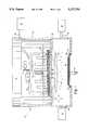
- FIG. 1is a side view of a plasma etching system of the present invention and wherein the aluminum shield and chamber have a portion cut away;
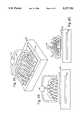
- FIGS. 2A, 2B and 2Care perspective, side and end views, respectively, of an inductor and coil positioned relative to an adjacent window on an enclosure and wherein the inductor and coil are similar to those shown in FIG. 1;
- FIG. 3is a perspective view of an alternative coil and capacitor embodiment of the present invention.
- FIG. 4is a perspective view of a still further alternative coil and capacitor embodiment of the present invention.
- FIG. 1illustrates a plasma etching system embodiment of the present invention, referred to by the general reference numeral 10, which comprises a vacuum variable capacitor 12 that is adjusted by a motor 14 through a gear train 16 and a main coil 18.
- Capacitor 12must be a high-voltage, high-current type, with a range of three picofarads to thirty picofarads.
- One manufacturer of suitable devicesis Jennings Corporation (San Jose, Calif.).
- the cost of such vacuum variable capacitorsis substantial.
- a parallel-series network of RF transmitter fixed capacitorssuch as made by High Energy Components (HEC) and CRL Components, can be substituted for vacuum variable capacitor 12, using adjustments in an external RF match.
- HECHigh Energy Components
- CRL Componentscan be substituted for vacuum variable capacitor 12, using adjustments in an external RF match.
- two parallel strings of four, fifteen KV capacitors rated at fifty picofarads eachcan be used with additional smaller capacitors added for rough trimming.
- This combinationhas given good results. (This combination Yields a combined capacitor of approximately twenty-eight picofarads at sixty Kv.)
- the loops of main coil 18are smaller and tighter together at the extremities of main coil 18, in order to shape a magnetic field 20 which, in turn, makes a planar plasma 22 more uniform.
- the outside loopswill be separated by 60% of the distance of the loop separation at the middle.
- Main coil 18may be constructed of 3/8 inch soft copper tubing, such as is commonly used for domestic plumbing. At radio frequencies, the majority of the current flowing in a conductor will be in the skin, so tubing functions very well and can be formed and flattened as needed. At one extreme, main coil 18 should have sufficient turns to maintain plasma 22 uniform, which is about five turns, minimum. At a maximum, main coil 18 should not include so many turns that the air gap distances between turns is so small that arcing occurs. Approximately fifteen turns is the maximum. Main coil 18 is typically twenty to thirty-five centimeters long, with a width at its widest part also typically twenty to thirty-five centimeters, and tapering down to ten to twenty centimeters across at each end.
- the resulting inductanceis approximately four to twenty microhenries.
- the separation space between turnsmay be maintained by plastic spacers.
- a plastic coil-formmay be used to give main coil 18 its shape and to improve its mechanical strength so that the shape does not deform in operation or in handling. Arcing between turns, if it becomes a problem, can be reduced or eliminated by immersing main coil 18 in an oil bath.
- the current carrying capabilities of main coil 18can be improved by silver plating the copper tubing from which it is constructed.
- the shape and size of main coil 18 and the spacing between turnsis typically empirically determined to obtain the desired magnetic and electric field distributions for a particular use.
- Main coil 18 and capacitor 12form a tank circuit having a natural frequency tunable by motor 14.
- a radio frequency (RF) generator 23provides power to an RF match 24, which provides an optimum power transfer into main coil 18.
- RF generator 23may be of the type generally used in the operation of semiconductor processing equipment and operable from about 13.56 MHz to 100 MHz, albeit 13.56 MHz is preferred.
- RF generator 23will usually have a low output impedance, typically fifty ohms, and it will be capable of producing 2.5 kilowatts.
- RF match 24may be a MATCHWORKS 25, as marketed by ENI Corporation, with has an auto-tuning/matching feature.
- RF match 24feeds a coupling coil 26.
- Coupling coil 26is preferably mounted near the center of main coil 18 and can be arranged so that it can be rotated to vary the coupling that occurs between it and main coil 18.
- An aluminum cylinder 29supports RF match 24 and helps contain the radiation of electromagnetic interference (EMI).
- Motor 14is used to match the tank circuit to the frequency of RF generator 24.
- the resultant transformer like couplingis such that field 20 is powerful enough to ignite and maintain plasma 22 within a chamber 30.
- An insulator 32is placed between an electrostatic shield 34 and main coil 18 to prevent arc-over.
- Electrostatic shield 34passes only electromagnetic fields and stops electrostatic fields from entering chamber 30.
- a planar window 36preferably of quartz, seals the interior of chamber 30 from the outside atmosphere and allows gases to be contained at vacuum pressures.
- Window 36allows magnetic field 20 to enter chamber 30, and is typically larger than the length and width of main coil 18.
- Main coil 18is preferably flattened on a side placed adjacent to window 36 so that the passage of field 20 through window 36 is improved.
- Window 36may be made of ceramic.
- a transparent window 36can allow an interferometer to be used at a light frequency not interfered with by plasma 22 to take measurements of the progress of activity within chamber 30.
- System 10further comprises an electrode 38 that is electrically insulated from chamber 30 by a ring insulator 40.
- a connector 42allows external electrical potentials to be applied to electrode 38 such that ions generated by plasma 22 may be attracted to a wafer 44 mounted on electrode 38.
- the longitudinal axis X--X of main coil 18is substantially parallel to plasma 22, window 36 and wafer 44. Electrons within plasma 22 will typically oscillate back and forth parallel to wafer 44 for a distance of approximately 4.5 centimeters. This relatively long distance of electron oscillation affords uniformity of plasma 22.
- the rate of change of current (dI/dt) within main coil 18produces the principal coupling mechanism with these electrons.
- The, so-called, non-uniformity of system 10has been measured to be better than five percent.
- Plasma 22is essentially two-dimensional and preferably does extend to the area of wafer 44. Ions produced in plasma 22 by the agitation of the electrons are typically accelerated in a direction "C" by electrode 38. Within chamber 30, there are preferably one or more surfaces for mounting an article or articles to be treated. Wafer 44 is typically a six-inch diameter wafer of silicon. Other embodiments of the present invention can create plasmas that are suitable for wafers twelve inches in diameter and larger. To accommodate the larger wafer sizes, the size of system 10, such as main coil 18 and chamber 30, is expanded proportionately. The flux density of ions created in plasma 22 may be controlled by adjusting the power output of generator 23. The ion energy of ions striking wafer 44 may be independently controlled by adjusting the electrical potential applied to electrode 38.
- a source of process gas 46supplies chamber 30 through an inlet port 48.
- a vacuum pump 50regulates the pressure within chamber 30 through an outlet port 52.
- Systems for supplying process gases and controlling the pressure within the enclosureare well known in the art and need not be further described.
- the ion densitywill, of course, be dependent on the gases and pressures used within chamber 30, because the density of plasma 22 depends on these parameters.
- FIGS. 2A, 2B and 2Cillustrate a main coil 60 and a capacitor 62 that are similar in function and purpose to main coil 18 and capacitor 12 in FIG. 1.
- a window 64allows a field generated by coil 60 to enter an enclosure 66 which has disposed within it a wafer 68 to be processed.
- Main coil 60includes a plurality of turns 70-77. As best shown in FIG. 2C, turns 70-77 are flattened adjacent to window 64. This allows a more intense varying magnetic field to enter enclosure 66.
- FIGS. 3 and 4illustrate alternative embodiments of that shown in FIGS. 2A-2C.
- a main coil 80includes a series of taps 81-87 that are connected to each turn.
- a capacitor 88is connected in parallel with main coil 80.
- a tap or set of taps near the center of main coil 80can thus be used to provide a path to ground or to a second source of electrostatic RF power to accelerate ions in chamber 30.
- Taps 81-87are connected respectively to a series of parallel elongated plates 91-97 on a dielectric window 98.
- the electrical connections of plates 91-97 to points on main coil 80are such that a portion of a voltage across the resonant circuit is more or less evenly distributed across the plates and will induce a planar plasma within an enclosure placed in close proximity and parallel to window 98.
- FIG. 4shows an alternative tapping arrangement. These taps can also be used to advantage on coils 18 and 60. Plasma generation using electric field coupling is sometimes more effective than magnetic field coupling for gas pressures above one hundred Pascals.
- a main coil 100includes a pair of taps 102 and 104 that are each connected to an outside coil turn.
- a capacitor 106connects to coil 100 and forms an inductive-capacitive resonant circuit. A very large voltage will develop between taps 102 and 104 when radio frequency power is coupled into coil 100 at the resonant frequency, e.g., by the method shown in FIG. 1.
- Taps 102 and 104are connected to a plurality of elongated planar plates 108, 110, 112 and 114 on a plane with a dielectric planar window 116.
- the electrical connections of plates 108, 110, 112 and 114 with main coil 80couple a voltage across the resonant circuit within the gas enclosure to induce a planar plasma within.
- the plasmawill be parallel to window 116.
- the electrostatic field induced into the gas enclosureis primarily responsible for the generation of the plasma and the magnetic field of coil 100 is reduced, or filtered out, by separating coil 100 from the gas enclosure.
- Plates 108, 110, 112 and 114are shaped as sections of a single circle in order to promote an outside circular boundary to the planar plasma. This particular shape is useful in semiconductor wafer processing because the wafers are typically round slices from a cylindrical boule of a crystal of semiconductor material.
- the theory of operation of embodiments of the present inventionmay be understood in terms of the electron mean free path in the process gas, the electron oscillation distance for ionization energy, and the dimensions of chamber 30.
- the electron mean free pathis defined as the average distance an electron travels between collisions with gas molecules. It is determined by the chamber gas pressure.
- the electron mean free pathis further affected by the size of the gas molecules, the energy of the electrons, and other factors. For a pressure of one Pascal, and a maximum energy of ten electron volts, the electron mean free path distance with common process gases will be approximately three centimeters. This distance varies inversely with the pressure.
- the electron oscillation distanceis approximately 4.4 centimeters. Since mass of an ion is so much greater than the mass of an electron, there will be no significant movement of the positive ions within plasma 22, assuming the power frequency remains 13.56 MHz.
- both the electron mean free path at a pressure of one Pascal and the electron oscillation distance for ionizing energyare greater than the spacing normally used between parallel plate electrodes in a plasma chamber. Therefore, an efficient plasma generation at pressures of one Pascal, or less, is not possible merely by applying RF power between a set of parallel electrodes.
- the chamber dimensions parallel to the electrodesare typically twenty to forty centimeters, so electrons with ionizing energy can undergo multiple oscillations parallel to wafer 44 without striking the electrodes or the chamber walls. This makes for high efficiency, in terms of conversion of electron energy to ionization energy, even for the relatively long electron mean free path at low pressure.
- the electron accelerating field due to the electric fieldis substantially parallel to the axis of the main coil, while the electron accelerating field due to the varying magnetic field is substantially parallel to the turns of the main coil adjacent to the window, which are substantially perpendicular to the axis of the main coil.
- the varying electric and magnetic fields from the main coil 18can be used for electron acceleration substantially parallel to surface of window 36 in the process gas inside chamber 30.
- Maximum coupling of both electric and magnetic fields from the main coil through the window into the chamberis provided with the main coil flattened on one side to form a series of bars adjacent to the window.
- Electric shield 34(FIG. 1), includes insulated conductors substantially parallel to the axis of the main coil 18 and window 36. The varying electric field passing through the window 36 into the chamber 30 is minimized, and the varying magnetic field dominates.
- FIG. 3shows that by mounting bars on posts and attaching them along the main coil parallel to the main coil axis, with the main coil spaced away from window 36 by the length of the posts, the magnetic field passing through the window is reduced and the electric field will dominate.
- the independent RF source used to accelerate the ions perpendicular to the waferis applied between the electrode on which the wafer is placed and an electrode formed either by the parallel bars of the main coil adjacent to the window or by an electric shield between the window and the main coil.
- This independent RF sourcecan be applied to either the wafer electrode 38 or the electrode formed by the main coil bars or the electric shield.
- ion density (flux) and ion energy (field)is possible because the plasma itself forms a relatively good conductor, separated from the chamber surfaces and the wafer by a relatively high impedance sheath, or dark space, so the voltage from one side of the plasma to the other is relatively small, while the voltage between the electrode formed by the bars and the other electrode can be large.
Landscapes
- Physics & Mathematics (AREA)
- Engineering & Computer Science (AREA)
- Plasma & Fusion (AREA)
- Chemical & Material Sciences (AREA)
- Analytical Chemistry (AREA)
- Plasma Technology (AREA)
- Chemical Vapour Deposition (AREA)
- Drying Of Semiconductors (AREA)
Abstract
Description
1. Field of the Invention
The present invention relates generally to systems and methods for producing low pressure plasmas. More particularly, it relates to equipment for producing highly uniform planar plasmas which can be used for treating semiconductor wafers in low pressure processing equipment.
Plasma generation is useful in a variety of semiconductor fabrication processes including etching, deposition, ion implantation and the like. Plasmas are generally produced in a low pressure gas by accelerating naturally occurring free electrons in the gas to the gas ionization energy, typically between five and twenty electron volts. Collisions between these energetic electrons and the gas molecules occasionally cause a molecule to be ionized, releasing an additional free electron. Each additional free electron is also accelerated and can also ionize gas molecules. The resultant partially ionized gas is called a plasma.
2. Description of the Prior Art
Most matter typically exists in one of four phases: solid, liquid, gas and plasma. Super hot plasmas are used in gas chromatographs to break down samples that have been injected so that they produce characteristic spectrums of light for analysis, and in semiconductor processing equipment to etch material away from a wafer. Plasma based semiconductor equipment also includes deposition processes, resist stripping and plasma enhanced chemical vapor deposition.
Larger and more uniform plasmas need to be generated now to keep pace with the ever increasing wafer sizes being processed. Whatever the step in the process, whether etching, depositing or implanting, the effects of the plasma typically need to be uniform across the entire surface. Present day technology includes eight inch wafer processing, and twelve inch wafer process fabrication facilities (fabs) are already being planned. The prior art equipment that was suitable for plasma etching two-inch wafers is unable to produce the uniformity that translates into maximum yields and better profits for state-of-the-art fabs.
Previous planar magnetically coupled plasma (PMCP) generating methods use a varying magnetic field generated by a planar spiral coil to generate the plasma, optionally combined with an independent radio frequency power source to accelerate the ions. This method is effective in providing independent control of flux and field with inexpensive equipment and simple operation through varying magnetic field electron acceleration. But it does not provide for uniform electron acceleration, especially near the axis of the coil. A prior art plasma etching system described by the present inventor in U.S. Pat. No. 4,948,458, issued Aug. 14, 1990, comprises a chamber with a dielectric window, such as quartz. A planar coil and capacitor combination is positioned adjacent to the window, with the axis of the coil perpendicular to the window, and a powerful radio frequency source is coupled to the coil. Power transfer is maximized by impedance matching and tuning to provide resonance at 13.56 MHz, for example. Inlet ports supply a process gas to the interior of the chamber. A varying magnetic field is induced by the coil into the process gas at power levels sufficient to create a plasma of the process gas that has a circulating flow of electrons. The electron motion is closely confined to a plane parallel to the planar coil, so transfer of kinetic energy in non-planar directions is minimal. The flow of electrons is planar, albeit annular, and therefore has an eye at the axis that has a lower energy level than the other parts of the planar plasma. The eye is unavoidable with a planar coil wound in a spiral, with the axis of the coil perpendicular to the plasma plane, as shown in FIGS. 1, 3, 6 and 7 of the patent.
A very common method for accelerating free electrons for plasmas in semiconductor wafer processing is to apply a radio frequency (RF) electric field between a pair of electrically conductive plates, or electrodes, on opposite sides of a process chamber that has been filled with a low pressure process gas. A wafer to be processed is typically mounted on one of these electrodes. As such, the RF electric field will accelerate electrons in the space between the electrodes with an ionization energy perpendicular to the surface of the wafer. The accelerated electrons will collide with process gas molecules, at a frequency dependent on the gas pressure. The collisions generate ions of gas which constitute the plasma. When the electrons strike the wafer, they are captured, and this results in a negative electric charge build up on the wafer. Such a charge will attract the positive ions circulating nearby in the plasma, and pull them to the wafer at high velocity. Whether the consequential ion impacts results in etching, deposition, or other effect, is a function of the type of gas generating the ions, the surface materials of the wafer, and other process conditions.
A single RF electric field will determine the levels of both the ion flux, which is the number of ions, and the ion field, which is the energy with which the ions strike the wafer. Independent control of the ion flux and field is therefore not easy to accomplish. However, some independent control of ion flux and field can be achieved by varying the gas pressure. As the gas pressure is lowered the distance between molecules increases, so electron collisions with molecules become less frequent. Since there are fewer collisions, there are fewer ions generated. Thus the ratio of ion flux to field is, in general, decreased. At pressures below approximately twenty pascals (0.15 torr), the ratio of ion flux to field becomes excessively low. Since pressures below twenty pascals are becoming increasingly important as semiconductor feature line widths decrease, the simple parallel plate method of plasma generation has recognized limitations. Several methods have been developed to circumvent the low pressure limitations of the parallel plate system.
In a magnetically enhanced plasma generation configuration, which is sometimes referred to as magnetically enhanced reactive ion etching (MERIE), a steady transverse magnetic field is used to curve the energized electron path. This increases the distance electrons must travel before they ultimately terminate in an electrode plate or wafer. While this method will increase the ion flux to field ratio, and permits a lower pressure for a given ratio, there are serious process disadvantages in having an intense transverse magnetic field so close to a wafer. This limits the lower pressure to approximately four pascals. U.S. Pat. Nos. 4,668,338, and 4,668,365, issued to Maydan, et al., and Foster, et al., respectively, describe a common approach to magnetically enhanced plasma generation.
Another prior art method, called electron cyclotron resonance (ECR), uses microwaves to accelerate the free electrons that create the plasma in a carefully controlled transverse magnetic field. The magnetic field is adjusted so that the rotation frequency of an electron, as deflected by the magnetic field, is equal to the microwave frequency. The electron energy is increased through a number of microwave power cycles until it reaches the ionization energy. For a microwave frequency of 2.45 GHz, the ECR magnetic field is 875 gauss. ECR plasma generation is often combined with a separate RF power source that is applied to an electrode on which the wafer is mounted. The separate source provides for ion acceleration. The microwave power therefore independently controls the ion flux and the RF power independently controls the ion field. While this method provides independent flux and field control, and can operate at low pressure, it also requires large and expensive magnets, combined with critical adjustments, for proper operation.
Other methods, in particular inductively coupled plasma (ICP) and helical inductor resonator (Helicon), are also used for plasma generation, but each has disadvantages in terms of efficiency, the ability to generate effective low pressure plasmas, and the ability to provide independent flux and field control. For more information on this subject, U.S. Pat. No. 4,421,690, describes an inductively coupled plasma (ICP) plasma generation apparatus, and U.S. Pat. No. 4,160,392, describes a helical inductive resonator plasma generation configuration.
Prior art plasma generation systems are not completely satisfactory in terms of their efficiency in generating a uniform planar plasma. Independent control of ion flux and field, in a simple, inexpensive configuration with no critical adjustments, is also lacking. While the planar magnetically coupled plasma system using a planar spiral coil is capable of satisfying most of these goals, there is a discontinuity in electron acceleration at the center of the coil that is an aberration in the desired plasma uniformity. However, there are advantages in providing transverse electron acceleration through the use of controlled amount of both electric and magnetic varying fields. At pressures below approximately ten pascals, an oscillating magnetic field is generally more efficient than an oscillating electric field in coupling energy to a plasma. However, an oscillating electric field may be needed to initiate the plasma. At pressures above approximately 100 pascals, an oscillating electric field is the more efficient.
An apparatus and method for generating highly uniform plasmas within semiconductor equipment is needed to support uses in etching, deposition and ion implantation equipment. Both electric and magnetic oscillating fields for acceleration of the ionizing electrons are desirable. The apparatus should preferably include a plasma generation capability that can generate high ion flux densities over a wide pressure range with a low ion energy directed toward a wafer being processed. An independent ion acceleration capability is needed for independent control of the ion flux and field to manage the ions striking the wafer. A simplicity of adjustment and operation, efficient operation in terms of power utilization, and small size are also goals that should be realized.
Therefore, an improvement in plasma generating technology is needed. The present invention overcomes the problems traditionally associated with plasma generation.
It is therefore an object of the present invention to provide a plasma through electron acceleration that is substantially parallel to and separated from a semiconductor wafer undergoing a process enabled by the plasma.
Briefly, an embodiment of the present invention is a plasma system that comprises a main coil with a flattened side and a capacitor that form a tuned circuit with radio frequency energy coupled to it through a radio frequency match by a generator. A process chamber with a quartz window and containing a low pressure gas is adjacent to the flat side of the main coil with the axis of the coil parallel to the surface of the window and a two-dimensional planar plasma in the shape of a circular disk is ignited and maintained by a high rate of change of the current flowing in the main coil. An electrode positioned in the chamber opposite to the window is used for attaching a semiconductor wafer for processing and a potential applied to the electrode independently controls the ion energy of ions attracted and accelerated out of the plasma.
An advantage of the present invention is that it provides a system in which ion density and energy are independently controllable.
A further advantage of the present invention is that a system is provided in which a planar plasma is produced that may be uniform over as much as a twelve inch diameter.
Another advantage of the present invention is that a system is provided in which plasmas may be ignited and maintained in process chamber pressures as low as one tenth of a Pascal.
These and other objects and advantages of the present invention will no doubt become obvious to those of ordinary skill in the art after having read the following detailed description of the preferred embodiments which are illustrated in the various drawing figures.
FIG. 1 is a side view of a plasma etching system of the present invention and wherein the aluminum shield and chamber have a portion cut away;
FIGS. 2A, 2B and 2C are perspective, side and end views, respectively, of an inductor and coil positioned relative to an adjacent window on an enclosure and wherein the inductor and coil are similar to those shown in FIG. 1;
FIG. 3 is a perspective view of an alternative coil and capacitor embodiment of the present invention; and
FIG. 4 is a perspective view of a still further alternative coil and capacitor embodiment of the present invention.
FIG. 1 illustrates a plasma etching system embodiment of the present invention, referred to by thegeneral reference numeral 10, which comprises avacuum variable capacitor 12 that is adjusted by amotor 14 through agear train 16 and amain coil 18.Capacitor 12 must be a high-voltage, high-current type, with a range of three picofarads to thirty picofarads. One manufacturer of suitable devices is Jennings Corporation (San Jose, Calif.). The cost of such vacuum variable capacitors is substantial. For a less expensive but still acceptable alternative, a parallel-series network of RF transmitter fixed capacitors, such as made by High Energy Components (HEC) and CRL Components, can be substituted forvacuum variable capacitor 12, using adjustments in an external RF match. For example, two parallel strings of four, fifteen KV capacitors rated at fifty picofarads each can be used with additional smaller capacitors added for rough trimming. This combination has given good results. (This combination Yields a combined capacitor of approximately twenty-eight picofarads at sixty Kv.) The loops ofmain coil 18 are smaller and tighter together at the extremities ofmain coil 18, in order to shape amagnetic field 20 which, in turn, makes aplanar plasma 22 more uniform. Typically the outside loops will be separated by 60% of the distance of the loop separation at the middle.
FIGS. 2A, 2B and 2C illustrate amain coil 60 and acapacitor 62 that are similar in function and purpose tomain coil 18 andcapacitor 12 in FIG. 1. Awindow 64 allows a field generated bycoil 60 to enter anenclosure 66 which has disposed within it awafer 68 to be processed.Main coil 60 includes a plurality of turns 70-77. As best shown in FIG. 2C, turns 70-77 are flattened adjacent towindow 64. This allows a more intense varying magnetic field to enterenclosure 66.
FIGS. 3 and 4 illustrate alternative embodiments of that shown in FIGS. 2A-2C. In FIG. 3, amain coil 80 includes a series of taps 81-87 that are connected to each turn. Acapacitor 88 is connected in parallel withmain coil 80. A tap or set of taps near the center ofmain coil 80 can thus be used to provide a path to ground or to a second source of electrostatic RF power to accelerate ions inchamber 30. Taps 81-87 are connected respectively to a series of parallel elongated plates 91-97 on adielectric window 98. The electrical connections of plates 91-97 to points onmain coil 80 are such that a portion of a voltage across the resonant circuit is more or less evenly distributed across the plates and will induce a planar plasma within an enclosure placed in close proximity and parallel towindow 98.
FIG. 4 shows an alternative tapping arrangement. These taps can also be used to advantage oncoils main coil 100 includes a pair oftaps capacitor 106 connects tocoil 100 and forms an inductive-capacitive resonant circuit. A very large voltage will develop betweentaps coil 100 at the resonant frequency, e.g., by the method shown in FIG. 1.Taps planar plates planar window 116. The electrical connections ofplates main coil 80 couple a voltage across the resonant circuit within the gas enclosure to induce a planar plasma within. The plasma will be parallel towindow 116. The electrostatic field induced into the gas enclosure is primarily responsible for the generation of the plasma and the magnetic field ofcoil 100 is reduced, or filtered out, by separatingcoil 100 from the gas enclosure.Plates
The theory of operation of embodiments of the present invention may be understood in terms of the electron mean free path in the process gas, the electron oscillation distance for ionization energy, and the dimensions ofchamber 30. The electron mean free path is defined as the average distance an electron travels between collisions with gas molecules. It is determined by the chamber gas pressure. The electron mean free path is further affected by the size of the gas molecules, the energy of the electrons, and other factors. For a pressure of one Pascal, and a maximum energy of ten electron volts, the electron mean free path distance with common process gases will be approximately three centimeters. This distance varies inversely with the pressure. For a sinusoidal electron oscillation with ten electron volts peak electron energy at an RF frequency of 13.56 MHz (a commonly used plasma generation frequency), the electron oscillation distance is approximately 4.4 centimeters. Since mass of an ion is so much greater than the mass of an electron, there will be no significant movement of the positive ions withinplasma 22, assuming the power frequency remains 13.56 MHz.
Both the electron mean free path at a pressure of one Pascal and the electron oscillation distance for ionizing energy are greater than the spacing normally used between parallel plate electrodes in a plasma chamber. Therefore, an efficient plasma generation at pressures of one Pascal, or less, is not possible merely by applying RF power between a set of parallel electrodes. In the present invention, such assystem 10, the chamber dimensions parallel to the electrodes are typically twenty to forty centimeters, so electrons with ionizing energy can undergo multiple oscillations parallel towafer 44 without striking the electrodes or the chamber walls. This makes for high efficiency, in terms of conversion of electron energy to ionization energy, even for the relatively long electron mean free path at low pressure.
The electron accelerating field due to the electric field is substantially parallel to the axis of the main coil, while the electron accelerating field due to the varying magnetic field is substantially parallel to the turns of the main coil adjacent to the window, which are substantially perpendicular to the axis of the main coil. Thus either or both the varying electric and magnetic fields from themain coil 18 can be used for electron acceleration substantially parallel to surface ofwindow 36 in the process gas insidechamber 30. Maximum coupling of both electric and magnetic fields from the main coil through the window into the chamber is provided with the main coil flattened on one side to form a series of bars adjacent to the window.
Since different applications, under different conditions, may benefit from either the electric or the magnetic field, either field can be made to dominate. Electric shield 34 (FIG. 1), includes insulated conductors substantially parallel to the axis of themain coil 18 andwindow 36. The varying electric field passing through thewindow 36 into thechamber 30 is minimized, and the varying magnetic field dominates. FIG. 3 shows that by mounting bars on posts and attaching them along the main coil parallel to the main coil axis, with the main coil spaced away fromwindow 36 by the length of the posts, the magnetic field passing through the window is reduced and the electric field will dominate.
The independent RF source used to accelerate the ions perpendicular to the wafer is applied between the electrode on which the wafer is placed and an electrode formed either by the parallel bars of the main coil adjacent to the window or by an electric shield between the window and the main coil. This independent RF source can be applied to either thewafer electrode 38 or the electrode formed by the main coil bars or the electric shield.
The separation of the two functions, ion density (flux) and ion energy (field) is possible because the plasma itself forms a relatively good conductor, separated from the chamber surfaces and the wafer by a relatively high impedance sheath, or dark space, so the voltage from one side of the plasma to the other is relatively small, while the voltage between the electrode formed by the bars and the other electrode can be large.
Although the present invention has been described in terms of the presently preferred embodiments, it is to be understood that the disclosure is not to be interpreted as limiting. Various alterations and modifications will no doubt become apparent to those skilled in the art after having read the above disclosure. Accordingly, it is intended that the appended claims be interpreted as covering all alterations and modifications as fall within the true spirit and scope of the invention.
Claims (14)
1. A method of planar plasma generation comprising the steps of:
winding a main coil of soft copper tubing having between five and fifteen turns including a flattening of said coil on one side;
connecting a high-current high-voltage capacitor to said flattened main coil;
positioning said flattened main coil proximate to a gas enclosure with said one flattened side adjacent to said gas enclosure;
coupling a radio frequency power source to said flattened main coil;
optimally coupling said radio frequency power to the combination of said main coil and capacitor with a matching means to result in the generation of a planar plasma within said gas enclosure that lies in a plane substantially parallel to the axis of said flattened main coil; and
filtering out the magnetic field of said main coil from reaching inside said gas enclosure by separating said coil and gas enclosure and communicating the potentials existing on a series of voltage taps on said main coil to a series of planar electrodes parallel to said gas enclosure wherein said planar plasma is generated by the varying electric field of said main coil.
2. An apparatus for producing a plasma, comprising:
a gas-tight enclosure bounded at least in part by a substantially planar electrically insulating window;
means for introducing a plurality of process gases into the enclosure;
means for controlling the pressure of said process gases;
a coil with a plurality of winding turns that progress along a longitudinal axis and positioned proximate to the enclosure and outside adjacent to said insulating window with said longitudinal axis of the coil oriented substantially parallel to said insulating window; and
means for coupling a radio frequency power source to the coil to cause a current to flow through the coil wherein a planar plasma may be ignited and maintained parallel to said insulating window.
3. The apparatus of claim 1, wherein:
a side of said coil adjacent to said window is flattened to substantially improve coupling between the coil and said plasma within the enclosure.
4. The apparatus of claim 1, further comprising:
an electrode mounted inside the enclosure opposite to said insulating window and having a connection for a source of radio frequency power wherein ions created within said plasma may be imparted an acceleration energy in the direction of the electrode.
5. The apparatus of claim 1, wherein:
a source of radio frequency power is applied between a point of said coil and a ground defined by the potential of the conductive portions of said enclosure.
6. An apparatus for producing a plasma, comprising:
an enclosure having an interior bounded at least in part by an electrically insulating window;
means for introducing a process gas into the enclosure;
means for controlling the pressure of said process gas while in the chamber;
a resonant circuit including at least one inductor and one capacitor; and
a series of elongated plates positioned side-by-side on said insulating window such that plates are substantially parallel, each plate including an electrical connection to points on said resonant circuit wherein a portion of a voltage across said resonant circuit also is distributed across the plates for inducing a planar plasma within the enclosure that is parallel to said window.
7. The apparatus of claim 6, further comprising:
means for generating a stable magnetic field having a field direction that is substantially perpendicular to said window.
8. The apparatus of claim 6, further comprising:
an electrode mounted inside the enclosure opposite to said insulating window; and
means for applying radio frequency power to said electrode.
9. An apparatus for treating articles with a plasma, said apparatus comprising:
an enclosure having an interior for supporting said articles to be treated, the enclosure being bounded at least in part by an electrically insulating window;
an electrically conductive coil mounted external to said enclosure adjacent to said window, with a longitudinal axis of said coil substantially parallel to the surface of said window for generating an intense varying internal magnetic field along said longitudinal axis and a weaker external return magnetic field outside the coil wherein a plasma may be maintained inside said plasma chamber by said weaker external return magnetic field passing through said window;
means for coupling radio frequency power to said coil to cause a radio frequency current to flow through said coil;
means for introducing process gases into said enclosure; and
means for controlling the pressure inside said chamber.
10. A plasma generation device for generating a substantially two-dimensional planar plasma parallel to a semiconductor wafer being processed, the device comprising:
a main coil including between five and fifteen turns wound along a longitudinal axis for generating an intense varying internal magnetic field along said longitudinal axis of the main coil and a weaker external return varying magnetic field outside the main coil, wherein said planar plasma may be maintained inside a plasma chamber by said weaker external return varying magnetic field passing through an adjacent insulating window;
a capacitor connected to the main coil for tuning the natural oscillating frequency of the combination of the main coil and capacitor;
a process chamber for receiving gas and supporting a substantially two-dimensional planar plasma parallel to the semiconductor wafer being processed, the process chamber having said adjacent insulating window in close proximity to the main coil and oriented with the axis of the main coil substantially parallel to the semiconductor wafer being processed;
means for radio frequency power injection coupled to the main coil wherein the two-dimensional planar plasma is generated; and
an electrode for accelerating ions produced from the two-dimensional planar plasma toward the semiconductor wafer in a direction normal to the plane of the semiconductor wafer.
11. The device of claim 10, wherein:
the main coil comprises soft copper tubing;
the capacitor is a vacuum variable type; and
said insulating window in the process chamber is a quartz window positioned between the main coil and the two-dimensional planar plasma.
12. The device of claim 10, further comprising:
an electrostatic shield is placed between the main coil and the two-dimensional planar plasma wherein only an electromagnetic field generated by the main coil is strong enough within the process chamber to ignite and maintain the two-dimensional planar plasma.
13. A system for generating a uniform planar plasma within a gas-tight, gas-filled plasma chamber with an electrically insulating window, comprising:
a coil with a plurality of winding turns that progress along a longitudinal axis and that is positioned proximate to the enclosure and outside adjacent to said insulating window with said longitudinal axis of the coil oriented substantially parallel to said insulating window for generating an intense varying internal magnetic field along said longitudinal axis and a weaker varying external return magnetic field outside the coil wherein a plasma may be maintained inside said plasma chamber by said weaker external return magnetic field passing through said insulating window.
14. A plasma generation device for generating a two-dimensional planar plasma parallel to a semiconductor wafer being processed, the device comprising:
a main coil including between five and fifteen turns wound along a longitudinal axis;
a capacitor connected to the main coil for tuning the natural oscillating frequency of the combination of the main coil and capacitor;
a process chamber for receiving gas and supporting a substantially two-dimensional planar plasma parallel to the semiconductor wafer being processed, the process chamber being in close proximity to the main coil and oriented with the axis of the main coil substantially parallel to the semiconductor wafer being processed;
means for radio frequency power injection coupled to the main coil wherein the two-dimensional planar plasma is generated;
an electrode for accelerating ions produced from the two-dimensional planar plasma toward the semiconductor wafer in a direction normal to the plane of the semiconductor wafer;
an electrostatic shield placed between the main coil and the two-dimensional planar system wherein only an electromagnetic field generated by the main coil is strong enough within the process chamber to ignite and maintain the two-dimensional planar plasma; and
an insulation layer that is placed between the main coil and the electrostatic shield for preventing electrical arcing of the main coil to the electrostatic shield.
Priority Applications (3)
| Application Number | Priority Date | Filing Date | Title |
|---|---|---|---|
| US07/900,131US5277751A (en) | 1992-06-18 | 1992-06-18 | Method and apparatus for producing low pressure planar plasma using a coil with its axis parallel to the surface of a coupling window |
| DE4319717ADE4319717A1 (en) | 1992-06-18 | 1993-06-15 | Device for generating planar low pressure plasma using a coil with its axis parallel to the surface of a coupling window |
| JP5145941AJP2591579B2 (en) | 1992-06-18 | 1993-06-17 | Plasma generator |
Applications Claiming Priority (1)
| Application Number | Priority Date | Filing Date | Title |
|---|---|---|---|
| US07/900,131US5277751A (en) | 1992-06-18 | 1992-06-18 | Method and apparatus for producing low pressure planar plasma using a coil with its axis parallel to the surface of a coupling window |
Publications (1)
| Publication Number | Publication Date |
|---|---|
| US5277751Atrue US5277751A (en) | 1994-01-11 |
Family
ID=25412020
Family Applications (1)
| Application Number | Title | Priority Date | Filing Date |
|---|---|---|---|
| US07/900,131Expired - LifetimeUS5277751A (en) | 1992-06-18 | 1992-06-18 | Method and apparatus for producing low pressure planar plasma using a coil with its axis parallel to the surface of a coupling window |
Country Status (3)
| Country | Link |
|---|---|
| US (1) | US5277751A (en) |
| JP (1) | JP2591579B2 (en) |
| DE (1) | DE4319717A1 (en) |
Cited By (155)
| Publication number | Priority date | Publication date | Assignee | Title |
|---|---|---|---|---|
| EP0658073A1 (en)* | 1993-12-08 | 1995-06-14 | Fujitsu Limited | Plasma generating apparatus and method |
| US5435881A (en)* | 1994-03-17 | 1995-07-25 | Ogle; John S. | Apparatus for producing planar plasma using varying magnetic poles |
| US5449433A (en)* | 1994-02-14 | 1995-09-12 | Micron Semiconductor, Inc. | Use of a high density plasma source having an electrostatic shield for anisotropic polysilicon etching over topography |
| US5464476A (en)* | 1993-10-19 | 1995-11-07 | Central Research Laboratories Limited | Plasma processing device comprising plural RF inductive coils |
| US5468296A (en)* | 1993-12-17 | 1995-11-21 | Lsi Logic Corporation | Apparatus for igniting low pressure inductively coupled plasma |
| US5472509A (en)* | 1993-11-30 | 1995-12-05 | Neomecs Incorporated | Gas plasma apparatus with movable film liners |
| US5504341A (en)* | 1995-02-17 | 1996-04-02 | Zimec Consulting, Inc. | Producing RF electric fields suitable for accelerating atomic and molecular ions in an ion implantation system |
| US5514246A (en)* | 1994-06-02 | 1996-05-07 | Micron Technology, Inc. | Plasma reactors and method of cleaning a plasma reactor |
| US5521351A (en)* | 1994-08-30 | 1996-05-28 | Wisconsin Alumni Research Foundation | Method and apparatus for plasma surface treatment of the interior of hollow forms |
| WO1996019910A1 (en)* | 1994-12-22 | 1996-06-27 | Research Triangle Institute | High frequency induction plasma method and apparatus |
| US5540824A (en)* | 1994-07-18 | 1996-07-30 | Applied Materials | Plasma reactor with multi-section RF coil and isolated conducting lid |
| US5540800A (en)* | 1994-06-23 | 1996-07-30 | Applied Materials, Inc. | Inductively coupled high density plasma reactor for plasma assisted materials processing |
| US5571366A (en)* | 1993-10-20 | 1996-11-05 | Tokyo Electron Limited | Plasma processing apparatus |
| US5589737A (en)* | 1994-12-06 | 1996-12-31 | Lam Research Corporation | Plasma processor for large workpieces |
| US5614055A (en)* | 1993-08-27 | 1997-03-25 | Applied Materials, Inc. | High density plasma CVD and etching reactor |
| US5622635A (en)* | 1993-01-19 | 1997-04-22 | International Business Machines Corporation | Method for enhanced inductive coupling to plasmas with reduced sputter contamination |
| US5667630A (en)* | 1995-04-28 | 1997-09-16 | Vanguard International Semiconductor Corporation | Low charge-up reactive ion metal etch process |
| US5674357A (en)* | 1995-08-30 | 1997-10-07 | Taiwan Semiconductor Manufacturing Company, Ltd. | Semiconductor substrate cleaning process |
| US5683537A (en)* | 1993-10-04 | 1997-11-04 | Tokyo Electron Limited | Plasma processing apparatus |
| US5688357A (en)* | 1995-02-15 | 1997-11-18 | Applied Materials, Inc. | Automatic frequency tuning of an RF power source of an inductively coupled plasma reactor |
| EP0807953A1 (en)* | 1996-05-13 | 1997-11-19 | Applied Materials, Inc. | Inductively coupled RF plasma reactor having an overhead solenoidal antenna |
| US5690781A (en)* | 1994-09-16 | 1997-11-25 | Nec Corporation | Plasma processing apparatus for manufacture of semiconductor devices |
| US5696428A (en)* | 1995-06-07 | 1997-12-09 | Lsi Logic Corporation | Apparatus and method using optical energy for specifying and quantitatively controlling chemically-reactive components of semiconductor processing plasma etching gas |
| US5753044A (en)* | 1995-02-15 | 1998-05-19 | Applied Materials, Inc. | RF plasma reactor with hybrid conductor and multi-radius dome ceiling |
| US5759921A (en)* | 1995-09-21 | 1998-06-02 | Lsi Logic Corporation | Integrated circuit device fabrication by plasma etching |
| US5785878A (en)* | 1995-11-02 | 1998-07-28 | Applied Materials, Inc. | RF antenna having high temperature, oxidation resistant coating |
| US5800619A (en)* | 1996-06-10 | 1998-09-01 | Lam Research Corporation | Vacuum plasma processor having coil with minimum magnetic field in its center |
| US5837615A (en)* | 1995-09-21 | 1998-11-17 | Lsi Logic Corporation | Integrated circuit device fabrication by plasma etching |
| US5858100A (en)* | 1994-04-06 | 1999-01-12 | Semiconductor Process Co., Ltd. | Substrate holder and reaction apparatus |
| WO1999029923A1 (en)* | 1997-12-05 | 1999-06-17 | Tegal Corporation | Plasma reactor with a deposition shield |
| US5922223A (en)* | 1995-11-16 | 1999-07-13 | Matsushita Electric Industrial Co., Ltd. | Plasma processing method and apparatus |
| US5938883A (en)* | 1993-01-12 | 1999-08-17 | Tokyo Electron Limited | Plasma processing apparatus |
| US5942855A (en)* | 1996-08-28 | 1999-08-24 | Northeastern University | Monolithic miniaturized inductively coupled plasma source |
| US5970907A (en)* | 1997-01-27 | 1999-10-26 | Canon Kabushiki Kaisha | Plasma processing apparatus |
| US5990017A (en)* | 1991-06-27 | 1999-11-23 | Applied Materials, Inc. | Plasma reactor with heated source of a polymer-hardening precursor material |
| US5994236A (en)* | 1998-01-23 | 1999-11-30 | Ogle; John Seldon | Plasma source with process nonuniformity improved using ferromagnetic cores |
| US6028285A (en)* | 1997-11-19 | 2000-02-22 | Board Of Regents, The University Of Texas System | High density plasma source for semiconductor processing |
| US6030508A (en)* | 1995-11-02 | 2000-02-29 | Taiwan Semiconductor Manufacturing Company | Sputter etching chamber having a gas baffle with improved uniformity |
| US6036878A (en)* | 1996-02-02 | 2000-03-14 | Applied Materials, Inc. | Low density high frequency process for a parallel-plate electrode plasma reactor having an inductive antenna |
| US6036877A (en)* | 1991-06-27 | 2000-03-14 | Applied Materials, Inc. | Plasma reactor with heated source of a polymer-hardening precursor material |
| US6054013A (en)* | 1996-02-02 | 2000-04-25 | Applied Materials, Inc. | Parallel plate electrode plasma reactor having an inductive antenna and adjustable radial distribution of plasma ion density |
| US6056848A (en)* | 1996-09-11 | 2000-05-02 | Ctp, Inc. | Thin film electrostatic shield for inductive plasma processing |
| US6063233A (en)* | 1991-06-27 | 2000-05-16 | Applied Materials, Inc. | Thermal control apparatus for inductively coupled RF plasma reactor having an overhead solenoidal antenna |
| US6074512A (en)* | 1991-06-27 | 2000-06-13 | Applied Materials, Inc. | Inductively coupled RF plasma reactor having an overhead solenoidal antenna and modular confinement magnet liners |
| US6074953A (en)* | 1998-08-28 | 2000-06-13 | Micron Technology, Inc. | Dual-source plasma etchers, dual-source plasma etching methods, and methods of forming planar coil dual-source plasma etchers |
| US6077384A (en)* | 1994-08-11 | 2000-06-20 | Applied Materials, Inc. | Plasma reactor having an inductive antenna coupling power through a parallel plate electrode |
| US6083412A (en)* | 1993-10-15 | 2000-07-04 | Applied Materials, Inc. | Plasma etch apparatus with heated scavenging surfaces |
| US6090303A (en)* | 1991-06-27 | 2000-07-18 | Applied Materials, Inc. | Process for etching oxides in an electromagnetically coupled planar plasma apparatus |
| US6132551A (en)* | 1997-09-20 | 2000-10-17 | Applied Materials, Inc. | Inductive RF plasma reactor with overhead coil and conductive laminated RF window beneath the overhead coil |
| US6136140A (en)* | 1993-01-12 | 2000-10-24 | Tokyo Electron Limited | Plasma processing apparatus |
| US6145469A (en)* | 1996-05-21 | 2000-11-14 | Canon Kabushiki Kaisha | Plasma processing apparatus and processing method |
| US6155199A (en)* | 1998-03-31 | 2000-12-05 | Lam Research Corporation | Parallel-antenna transformer-coupled plasma generation system |
| US6164241A (en)* | 1998-06-30 | 2000-12-26 | Lam Research Corporation | Multiple coil antenna for inductively-coupled plasma generation systems |
| US6177646B1 (en)* | 1997-03-17 | 2001-01-23 | Matsushita Electric Industrial Co, Ltd. | Method and device for plasma treatment |
| US6204607B1 (en) | 1998-05-28 | 2001-03-20 | Applied Komatsu Technology, Inc. | Plasma source with multiple magnetic flux sources each having a ferromagnetic core |
| US6229264B1 (en) | 1999-03-31 | 2001-05-08 | Lam Research Corporation | Plasma processor with coil having variable rf coupling |
| US6238588B1 (en) | 1991-06-27 | 2001-05-29 | Applied Materials, Inc. | High pressure high non-reactive diluent gas content high plasma ion density plasma oxide etch process |
| US6237526B1 (en) | 1999-03-26 | 2001-05-29 | Tokyo Electron Limited | Process apparatus and method for improving plasma distribution and performance in an inductively coupled plasma |
| US6248250B1 (en) | 1995-02-15 | 2001-06-19 | Applied Materials Inc. | RF plasma reactor with hybrid conductor and multi-radius dome ceiling |
| US6270617B1 (en) | 1995-02-15 | 2001-08-07 | Applied Materials, Inc. | RF plasma reactor with hybrid conductor and multi-radius dome ceiling |
| US6291358B1 (en) | 1999-10-15 | 2001-09-18 | Micron Technology, Inc. | Plasma deposition tool operating method |
| US6297468B1 (en) | 1994-10-31 | 2001-10-02 | Applied Materials, Inc. | Inductively coupled plasma reactor with symmetrical parallel multiple coils having a common RF terminal |
| US6319355B1 (en) | 1999-06-30 | 2001-11-20 | Lam Research Corporation | Plasma processor with coil responsive to variable amplitude rf envelope |
| US6338313B1 (en) | 1995-07-19 | 2002-01-15 | Silison Genesis Corporation | System for the plasma treatment of large area substrates |
| US6348126B1 (en) | 2000-08-11 | 2002-02-19 | Applied Materials, Inc. | Externally excited torroidal plasma source |
| US6369348B2 (en) | 1997-06-30 | 2002-04-09 | Applied Materials, Inc | Plasma reactor with coil antenna of plural helical conductors with equally spaced ends |
| US6401652B1 (en) | 2000-05-04 | 2002-06-11 | Applied Materials, Inc. | Plasma reactor inductive coil antenna with flat surface facing the plasma |
| US6410449B1 (en) | 2000-08-11 | 2002-06-25 | Applied Materials, Inc. | Method of processing a workpiece using an externally excited torroidal plasma source |
| US6409933B1 (en) | 2000-07-06 | 2002-06-25 | Applied Materials, Inc. | Plasma reactor having a symmetric parallel conductor coil antenna |
| US6414648B1 (en) | 2000-07-06 | 2002-07-02 | Applied Materials, Inc. | Plasma reactor having a symmetric parallel conductor coil antenna |
| US6418874B1 (en) | 2000-05-25 | 2002-07-16 | Applied Materials, Inc. | Toroidal plasma source for plasma processing |
| US6441555B1 (en) | 2000-03-31 | 2002-08-27 | Lam Research Corporation | Plasma excitation coil |
| US6440221B2 (en) | 1996-05-13 | 2002-08-27 | Applied Materials, Inc. | Process chamber having improved temperature control |
| US6451161B1 (en)* | 2000-04-10 | 2002-09-17 | Nano-Architect Research Corporation | Method and apparatus for generating high-density uniform plasma |
| US6453842B1 (en) | 2000-08-11 | 2002-09-24 | Applied Materials Inc. | Externally excited torroidal plasma source using a gas distribution plate |
| US6458723B1 (en) | 1999-06-24 | 2002-10-01 | Silicon Genesis Corporation | High temperature implant apparatus |
| US6462481B1 (en) | 2000-07-06 | 2002-10-08 | Applied Materials Inc. | Plasma reactor having a symmetric parallel conductor coil antenna |
| US6465051B1 (en) | 1994-04-28 | 2002-10-15 | Applied Materials, Inc. | Method of operating high density plasma CVD reactor with combined inductive and capacitive coupling |
| US6464843B1 (en) | 1998-03-31 | 2002-10-15 | Lam Research Corporation | Contamination controlling method and apparatus for a plasma processing chamber |
| US6468388B1 (en) | 2000-08-11 | 2002-10-22 | Applied Materials, Inc. | Reactor chamber for an externally excited torroidal plasma source with a gas distribution plate |
| WO2002086943A1 (en)* | 2001-04-23 | 2002-10-31 | Tokyo Electron Limited | Apparatus and method for improving plasma distribution and performance in an inductively coupled plasma |
| US6488807B1 (en) | 1991-06-27 | 2002-12-03 | Applied Materials, Inc. | Magnetic confinement in a plasma reactor having an RF bias electrode |
| US6494986B1 (en) | 2000-08-11 | 2002-12-17 | Applied Materials, Inc. | Externally excited multiple torroidal plasma source |
| US6494998B1 (en) | 2000-08-30 | 2002-12-17 | Tokyo Electron Limited | Process apparatus and method for improving plasma distribution and performance in an inductively coupled plasma using an internal inductive element |
| US6514838B2 (en) | 1998-02-17 | 2003-02-04 | Silicon Genesis Corporation | Method for non mass selected ion implant profile control |
| US6514376B1 (en) | 1991-06-27 | 2003-02-04 | Applied Materials Inc. | Thermal control apparatus for inductively coupled RF plasma reactor having an overhead solenoidal antenna |
| US6523493B1 (en)* | 2000-08-01 | 2003-02-25 | Tokyo Electron Limited | Ring-shaped high-density plasma source and method |
| US6527912B2 (en) | 2001-03-30 | 2003-03-04 | Lam Research Corporation | Stacked RF excitation coil for inductive plasma processor |
| US20030047449A1 (en)* | 2000-08-11 | 2003-03-13 | Applied Materials, Inc. | Method to drive spatially separate resonant structure with spatially distinct plasma secondaries using a single generator and switching elements |
| US6551446B1 (en) | 2000-08-11 | 2003-04-22 | Applied Materials Inc. | Externally excited torroidal plasma source with a gas distribution plate |
| US6572732B2 (en) | 1992-12-01 | 2003-06-03 | Applied Materials Inc. | Parallel-plate electrode plasma reactor having an inductive antenna coupling power through a parallel plate electrode |
| US6589437B1 (en) | 1999-03-05 | 2003-07-08 | Applied Materials, Inc. | Active species control with time-modulated plasma |
| US20030226641A1 (en)* | 2000-08-11 | 2003-12-11 | Applied Materials, Inc. | Externally excited torroidal plasma source with magnetic control of ion distribution |
| US6685798B1 (en) | 2000-07-06 | 2004-02-03 | Applied Materials, Inc | Plasma reactor having a symmetrical parallel conductor coil antenna |
| US6694915B1 (en) | 2000-07-06 | 2004-02-24 | Applied Materials, Inc | Plasma reactor having a symmetrical parallel conductor coil antenna |
| US6712927B1 (en) | 1998-06-11 | 2004-03-30 | Applied Materials Inc. | Chamber having process monitoring window |
| US20040079287A1 (en)* | 1997-06-26 | 2004-04-29 | Applied Science & Technology, Inc. | Toroidal low-field reactive gas source |
| US20040107907A1 (en)* | 2000-08-11 | 2004-06-10 | Applied Materials, Inc. | Plasma immersion ion implantation system including a plasma source having low dissociation and low minimum plasma voltage |
| US20040107906A1 (en)* | 2000-08-11 | 2004-06-10 | Applied Materials, Inc. | Plasma immersion ion implantation apparatus including a plasma source having low dissociation and low minimum plasma voltage |
| US20040149218A1 (en)* | 2000-08-11 | 2004-08-05 | Applied Materials, Inc. | Plasma immersion ion implantation process using a capacitively coupled plasma source having low dissociation and low minimum plasma voltage |
| US20040165180A1 (en)* | 2003-02-20 | 2004-08-26 | David Voeller | Method and apparatus for vehicle service system with imaging components |
| US6783629B2 (en) | 2002-03-11 | 2004-08-31 | Yuri Glukhoy | Plasma treatment apparatus with improved uniformity of treatment and method for improving uniformity of plasma treatment |
| US20040175953A1 (en)* | 2003-03-07 | 2004-09-09 | Ogle John S. | Apparatus for generating planar plasma using concentric coils and ferromagnetic cores |
| US20040200417A1 (en)* | 2002-06-05 | 2004-10-14 | Applied Materials, Inc. | Very low temperature CVD process with independently variable conformality, stress and composition of the CVD layer |
| US20050051272A1 (en)* | 2000-08-11 | 2005-03-10 | Applied Materials, Inc. | Plasma immersion ion implantation process using an inductively coupled plasma source having low dissociation and low minimum plasma voltage |
| US20050070073A1 (en)* | 2000-08-11 | 2005-03-31 | Applied Materials, Inc. | Silicon-on-insulator wafer transfer method using surface activation plasma immersion ion implantation for wafer-to-wafer adhesion enhancement |
| US6893907B2 (en) | 2002-06-05 | 2005-05-17 | Applied Materials, Inc. | Fabrication of silicon-on-insulator structure using plasma immersion ion implantation |
| US20050128160A1 (en)* | 2002-12-31 | 2005-06-16 | Lam Research Corporation | Antenna for plasma processor apparatus |
| US20050136604A1 (en)* | 2000-08-10 | 2005-06-23 | Amir Al-Bayati | Semiconductor on insulator vertical transistor fabrication and doping process |
| US6924455B1 (en) | 1997-06-26 | 2005-08-02 | Applied Science & Technology, Inc. | Integrated plasma chamber and inductively-coupled toroidal plasma source |
| US20050191828A1 (en)* | 2000-08-11 | 2005-09-01 | Applied Materials, Inc. | Method for ion implanting insulator material to reduce dielectric constant |
| US20050191827A1 (en)* | 2000-08-11 | 2005-09-01 | Collins Kenneth S. | Plasma immersion ion implantation process |
| US20050214478A1 (en)* | 2004-03-26 | 2005-09-29 | Applied Materials, Inc. | Chemical vapor deposition plasma process using plural ion shower grids |
| US20050211171A1 (en)* | 2004-03-26 | 2005-09-29 | Applied Materials, Inc. | Chemical vapor deposition plasma reactor having an ion shower grid |
| US20050214477A1 (en)* | 2004-03-26 | 2005-09-29 | Applied Materials, Inc. | Chemical vapor deposition plasma process using an ion shower grid |
| US20050211170A1 (en)* | 2004-03-26 | 2005-09-29 | Applied Materials, Inc. | Chemical vapor deposition plasma reactor having plural ion shower grids |
| US20050211547A1 (en)* | 2004-03-26 | 2005-09-29 | Applied Materials, Inc. | Reactive sputter deposition plasma reactor and process using plural ion shower grids |
| US20050211546A1 (en)* | 2004-03-26 | 2005-09-29 | Applied Materials, Inc. | Reactive sputter deposition plasma process using an ion shower grid |
| US20050224181A1 (en)* | 2004-04-08 | 2005-10-13 | Applied Materials, Inc. | Method and apparatus for in-situ film stack processing |
| US20050230047A1 (en)* | 2000-08-11 | 2005-10-20 | Applied Materials, Inc. | Plasma immersion ion implantation apparatus |
| US20050257742A1 (en)* | 2000-06-07 | 2005-11-24 | Tue Nguyen | Replaceable shielding apparatus |
| US20060019477A1 (en)* | 2004-07-20 | 2006-01-26 | Hiroji Hanawa | Plasma immersion ion implantation reactor having an ion shower grid |
| US20060019039A1 (en)* | 2004-07-20 | 2006-01-26 | Applied Materials, Inc. | Plasma immersion ion implantation reactor having multiple ion shower grids |
| US20060043065A1 (en)* | 2004-08-26 | 2006-03-02 | Applied Materials, Inc. | Gasless high voltage high contact force wafer contact-cooling electrostatic chuck |
| US20060081558A1 (en)* | 2000-08-11 | 2006-04-20 | Applied Materials, Inc. | Plasma immersion ion implantation process |
| US20060088655A1 (en)* | 2004-10-23 | 2006-04-27 | Applied Materials, Inc. | RF measurement feedback control and diagnostics for a plasma immersion ion implantation reactor |
| US7094316B1 (en) | 2000-08-11 | 2006-08-22 | Applied Materials, Inc. | Externally excited torroidal plasma source |
| US7094670B2 (en) | 2000-08-11 | 2006-08-22 | Applied Materials, Inc. | Plasma immersion ion implantation process |
| US7109098B1 (en) | 2005-05-17 | 2006-09-19 | Applied Materials, Inc. | Semiconductor junction formation process including low temperature plasma deposition of an optical absorption layer and high speed optical annealing |
| US20060237136A1 (en)* | 2005-04-26 | 2006-10-26 | Andrew Nguyen | O-ringless tandem throttle valve for a plasma reactor chamber |
| US20060263540A1 (en)* | 2005-05-17 | 2006-11-23 | Kartik Ramaswamy | Process for low temperature plasma deposition of an optical absorption layer and high speed optical annealing |
| US20060260545A1 (en)* | 2005-05-17 | 2006-11-23 | Kartik Ramaswamy | Low temperature absorption layer deposition and high speed optical annealing system |
| US20060264060A1 (en)* | 2005-05-17 | 2006-11-23 | Kartik Ramaswamy | Low temperature plasma deposition process for carbon layer deposition |
| KR100606622B1 (en)* | 1994-12-06 | 2006-12-01 | 램 리써치 코포레이션 | Plasma processoror for large workpieces |
| US7166816B1 (en) | 1997-06-26 | 2007-01-23 | Mks Instruments, Inc. | Inductively-coupled torodial plasma source |
| US20070032054A1 (en)* | 2005-08-08 | 2007-02-08 | Applied Materials, Inc. | Semiconductor substrate process using a low temperature deposited carbon-containing hard mask |
| US20070032082A1 (en)* | 2005-08-08 | 2007-02-08 | Applied Materials, Inc. | Semiconductor substrate process using an optically writable carbon-containing mask |
| US20070032095A1 (en)* | 2005-08-08 | 2007-02-08 | Applied Materials, Inc. | Copper conductor annealing process employing high speed optical annealing with a low temperature-deposited optical absorber layer |
| US20070032004A1 (en)* | 2005-08-08 | 2007-02-08 | Applied Materials, Inc. | Copper barrier reflow process employing high speed optical annealing |
| US20070042580A1 (en)* | 2000-08-10 | 2007-02-22 | Amir Al-Bayati | Ion implanted insulator material with reduced dielectric constant |
| US20070123931A1 (en)* | 1997-11-07 | 2007-05-31 | Salviac Limited | Embolic protection system |
| US20080011600A1 (en)* | 2006-07-14 | 2008-01-17 | Makoto Nagashima | Dual hexagonal shaped plasma source |
| US20080122367A1 (en)* | 2006-11-29 | 2008-05-29 | Foi Corporation | Apparatus and method for plasma processing |
| US20080173237A1 (en)* | 2007-01-19 | 2008-07-24 | Collins Kenneth S | Plasma Immersion Chamber |
| US7439188B2 (en) | 1999-12-02 | 2008-10-21 | Tegal Corporation | Reactor with heated and textured electrodes and surfaces |
| USRE40963E1 (en)* | 1993-01-12 | 2009-11-10 | Tokyo Electron Limited | Method for plasma processing by shaping an induced electric field |
| US20090288772A1 (en)* | 1997-06-26 | 2009-11-26 | Mks Instruments, Inc. | Method and Apparatus for Processing Metal Bearing Gases |
| US20100269980A1 (en)* | 2009-04-28 | 2010-10-28 | Tokyo Electron Limited | Plasma processing apparatus |
| US8779322B2 (en) | 1997-06-26 | 2014-07-15 | Mks Instruments Inc. | Method and apparatus for processing metal bearing gases |
| CN103974517A (en)* | 2014-05-22 | 2014-08-06 | 哈尔滨工业大学 | Constraint plasma aggregator under condition of high frequency electromagnetic field and aggregation method achieved by adoption of same |
| US20150251214A1 (en)* | 2011-10-14 | 2015-09-10 | Applied Materials, Inc. | Method and apparatus for aligning nanowires deposited by an electrospinning process |
| US20150318146A1 (en)* | 2014-04-30 | 2015-11-05 | Semes Co., Ltd. | System and method for treating substrate |
| US11037765B2 (en)* | 2018-07-03 | 2021-06-15 | Tokyo Electron Limited | Resonant structure for electron cyclotron resonant (ECR) plasma ionization |
| US20210293639A1 (en)* | 2018-08-08 | 2021-09-23 | Suzhou Phaserise Technology Co., Ltd. | Electromagnetic ultrasonic double-wave transducer |
| US20220025519A1 (en)* | 2018-10-26 | 2022-01-27 | Lpe S.P.A. | Deposition reactor with inductors and electromagnetic shields |
Families Citing this family (5)
| Publication number | Priority date | Publication date | Assignee | Title |
|---|---|---|---|---|
| JP2845199B2 (en)* | 1996-06-14 | 1999-01-13 | 日本電気株式会社 | Dry etching apparatus and dry etching method |
| US6534922B2 (en) | 1996-09-27 | 2003-03-18 | Surface Technology Systems, Plc | Plasma processing apparatus |
| KR100505176B1 (en) | 1996-09-27 | 2005-10-10 | 서페이스 테크놀로지 시스템스 피엘씨 | Plasma Processing Equipment |
| DE10058768C2 (en)* | 2000-11-27 | 2003-08-21 | Singulus Technologies Ag | Process for igniting a plasma |
| DE102015003379A1 (en)* | 2015-03-17 | 2016-09-22 | Manz Ag | Plasma generating device with an induction coil |
Citations (5)
| Publication number | Priority date | Publication date | Assignee | Title |
|---|---|---|---|---|
| US3705091A (en)* | 1971-10-05 | 1972-12-05 | Lfe Corp | Gas discharge apparatus |
| US4123316A (en)* | 1975-10-06 | 1978-10-31 | Hitachi, Ltd. | Plasma processor |
| US4786352A (en)* | 1986-09-12 | 1988-11-22 | Benzing Technologies, Inc. | Apparatus for in-situ chamber cleaning |
| US4810935A (en)* | 1985-05-03 | 1989-03-07 | The Australian National University | Method and apparatus for producing large volume magnetoplasmas |
| US4948458A (en)* | 1989-08-14 | 1990-08-14 | Lam Research Corporation | Method and apparatus for producing magnetically-coupled planar plasma |
Family Cites Families (4)
| Publication number | Priority date | Publication date | Assignee | Title |
|---|---|---|---|---|
| US4362632A (en)* | 1974-08-02 | 1982-12-07 | Lfe Corporation | Gas discharge apparatus |
| US4668388A (en)* | 1983-11-25 | 1987-05-26 | Texaco Inc. | High rate sludge reactor |
| US4668365A (en)* | 1984-10-25 | 1987-05-26 | Applied Materials, Inc. | Apparatus and method for magnetron-enhanced plasma-assisted chemical vapor deposition |
| GB8905075D0 (en)* | 1989-03-06 | 1989-04-19 | Nordiko Ltd | Electrode assembly and apparatus |
- 1992
- 1992-06-18USUS07/900,131patent/US5277751A/ennot_activeExpired - Lifetime
- 1993
- 1993-06-15DEDE4319717Apatent/DE4319717A1/ennot_activeCeased
- 1993-06-17JPJP5145941Apatent/JP2591579B2/ennot_activeExpired - Fee Related
Patent Citations (5)
| Publication number | Priority date | Publication date | Assignee | Title |
|---|---|---|---|---|
| US3705091A (en)* | 1971-10-05 | 1972-12-05 | Lfe Corp | Gas discharge apparatus |
| US4123316A (en)* | 1975-10-06 | 1978-10-31 | Hitachi, Ltd. | Plasma processor |
| US4810935A (en)* | 1985-05-03 | 1989-03-07 | The Australian National University | Method and apparatus for producing large volume magnetoplasmas |
| US4786352A (en)* | 1986-09-12 | 1988-11-22 | Benzing Technologies, Inc. | Apparatus for in-situ chamber cleaning |
| US4948458A (en)* | 1989-08-14 | 1990-08-14 | Lam Research Corporation | Method and apparatus for producing magnetically-coupled planar plasma |
Cited By (254)
| Publication number | Priority date | Publication date | Assignee | Title |
|---|---|---|---|---|
| US6063233A (en)* | 1991-06-27 | 2000-05-16 | Applied Materials, Inc. | Thermal control apparatus for inductively coupled RF plasma reactor having an overhead solenoidal antenna |
| US5990017A (en)* | 1991-06-27 | 1999-11-23 | Applied Materials, Inc. | Plasma reactor with heated source of a polymer-hardening precursor material |
| US6036877A (en)* | 1991-06-27 | 2000-03-14 | Applied Materials, Inc. | Plasma reactor with heated source of a polymer-hardening precursor material |
| US6444085B1 (en) | 1991-06-27 | 2002-09-03 | Applied Materials Inc. | Inductively coupled RF plasma reactor having an antenna adjacent a window electrode |
| US6488807B1 (en) | 1991-06-27 | 2002-12-03 | Applied Materials, Inc. | Magnetic confinement in a plasma reactor having an RF bias electrode |
| US6736931B2 (en) | 1991-06-27 | 2004-05-18 | Kenneth S. Collins | Inductively coupled RF plasma reactor and plasma chamber enclosure structure therefor |
| US6440866B1 (en) | 1991-06-27 | 2002-08-27 | Applied Materials, Inc. | Plasma reactor with heated source of a polymer-hardening precursor material |
| US6790311B2 (en) | 1991-06-27 | 2004-09-14 | Kenneth S Collins | Plasma reactor having RF power applicator and a dual-purpose window |
| US6514376B1 (en) | 1991-06-27 | 2003-02-04 | Applied Materials Inc. | Thermal control apparatus for inductively coupled RF plasma reactor having an overhead solenoidal antenna |
| US6090303A (en)* | 1991-06-27 | 2000-07-18 | Applied Materials, Inc. | Process for etching oxides in an electromagnetically coupled planar plasma apparatus |
| US6454898B1 (en) | 1991-06-27 | 2002-09-24 | Applied Materials, Inc. | Inductively coupled RF Plasma reactor having an overhead solenoidal antenna and modular confinement magnet liners |
| US6074512A (en)* | 1991-06-27 | 2000-06-13 | Applied Materials, Inc. | Inductively coupled RF plasma reactor having an overhead solenoidal antenna and modular confinement magnet liners |
| US6165311A (en)* | 1991-06-27 | 2000-12-26 | Applied Materials, Inc. | Inductively coupled RF plasma reactor having an overhead solenoidal antenna |
| US6238588B1 (en) | 1991-06-27 | 2001-05-29 | Applied Materials, Inc. | High pressure high non-reactive diluent gas content high plasma ion density plasma oxide etch process |
| US6572732B2 (en) | 1992-12-01 | 2003-06-03 | Applied Materials Inc. | Parallel-plate electrode plasma reactor having an inductive antenna coupling power through a parallel plate electrode |
| US6623596B1 (en) | 1992-12-01 | 2003-09-23 | Applied Materials, Inc | Plasma reactor having an inductive antenna coupling power through a parallel plate electrode |
| USRE40963E1 (en)* | 1993-01-12 | 2009-11-10 | Tokyo Electron Limited | Method for plasma processing by shaping an induced electric field |
| US6265031B1 (en) | 1993-01-12 | 2001-07-24 | Tokyo Electron Limited | Method for plasma processing by shaping an induced electric field |
| US5938883A (en)* | 1993-01-12 | 1999-08-17 | Tokyo Electron Limited | Plasma processing apparatus |
| US6136140A (en)* | 1993-01-12 | 2000-10-24 | Tokyo Electron Limited | Plasma processing apparatus |
| US6136139A (en)* | 1993-01-12 | 2000-10-24 | Tokyo Electron Limited | Plasma processing apparatus |
| US5622635A (en)* | 1993-01-19 | 1997-04-22 | International Business Machines Corporation | Method for enhanced inductive coupling to plasmas with reduced sputter contamination |
| US5614055A (en)* | 1993-08-27 | 1997-03-25 | Applied Materials, Inc. | High density plasma CVD and etching reactor |
| US5683537A (en)* | 1993-10-04 | 1997-11-04 | Tokyo Electron Limited | Plasma processing apparatus |
| US6083412A (en)* | 1993-10-15 | 2000-07-04 | Applied Materials, Inc. | Plasma etch apparatus with heated scavenging surfaces |
| US5464476A (en)* | 1993-10-19 | 1995-11-07 | Central Research Laboratories Limited | Plasma processing device comprising plural RF inductive coils |
| US5571366A (en)* | 1993-10-20 | 1996-11-05 | Tokyo Electron Limited | Plasma processing apparatus |
| US5472509A (en)* | 1993-11-30 | 1995-12-05 | Neomecs Incorporated | Gas plasma apparatus with movable film liners |
| EP0658073A1 (en)* | 1993-12-08 | 1995-06-14 | Fujitsu Limited | Plasma generating apparatus and method |
| US5513765A (en)* | 1993-12-08 | 1996-05-07 | Fujitsu Limited | Plasma generating apparatus and method |
| US5639519A (en)* | 1993-12-17 | 1997-06-17 | Lsi Logic Corporation | Method for igniting low pressure inductively coupled plasma |
| US6062163A (en)* | 1993-12-17 | 2000-05-16 | Lsi Logic Corporation | Plasma initiating assembly |
| US5468296A (en)* | 1993-12-17 | 1995-11-21 | Lsi Logic Corporation | Apparatus for igniting low pressure inductively coupled plasma |
| US5449433A (en)* | 1994-02-14 | 1995-09-12 | Micron Semiconductor, Inc. | Use of a high density plasma source having an electrostatic shield for anisotropic polysilicon etching over topography |
| US5435881A (en)* | 1994-03-17 | 1995-07-25 | Ogle; John S. | Apparatus for producing planar plasma using varying magnetic poles |
| US5858100A (en)* | 1994-04-06 | 1999-01-12 | Semiconductor Process Co., Ltd. | Substrate holder and reaction apparatus |
| US6465051B1 (en) | 1994-04-28 | 2002-10-15 | Applied Materials, Inc. | Method of operating high density plasma CVD reactor with combined inductive and capacitive coupling |
| US5779849A (en)* | 1994-06-02 | 1998-07-14 | Micron Technology, Inc. | Plasma reactors and method of cleaning a plasma reactor |
| US5647913A (en)* | 1994-06-02 | 1997-07-15 | Micron Technology, Inc. | Plasma reactors |
| US5514246A (en)* | 1994-06-02 | 1996-05-07 | Micron Technology, Inc. | Plasma reactors and method of cleaning a plasma reactor |
| US5980688A (en)* | 1994-06-02 | 1999-11-09 | Micron Technology, Inc. | Plasma reactors and method of cleaning a plasma reactor |
| US5540800A (en)* | 1994-06-23 | 1996-07-30 | Applied Materials, Inc. | Inductively coupled high density plasma reactor for plasma assisted materials processing |
| US5540824A (en)* | 1994-07-18 | 1996-07-30 | Applied Materials | Plasma reactor with multi-section RF coil and isolated conducting lid |
| US6077384A (en)* | 1994-08-11 | 2000-06-20 | Applied Materials, Inc. | Plasma reactor having an inductive antenna coupling power through a parallel plate electrode |
| US5521351A (en)* | 1994-08-30 | 1996-05-28 | Wisconsin Alumni Research Foundation | Method and apparatus for plasma surface treatment of the interior of hollow forms |
| US5690781A (en)* | 1994-09-16 | 1997-11-25 | Nec Corporation | Plasma processing apparatus for manufacture of semiconductor devices |
| US6297468B1 (en) | 1994-10-31 | 2001-10-02 | Applied Materials, Inc. | Inductively coupled plasma reactor with symmetrical parallel multiple coils having a common RF terminal |
| US5589737A (en)* | 1994-12-06 | 1996-12-31 | Lam Research Corporation | Plasma processor for large workpieces |
| KR100606622B1 (en)* | 1994-12-06 | 2006-12-01 | 램 리써치 코포레이션 | Plasma processoror for large workpieces |
| US5643639A (en)* | 1994-12-22 | 1997-07-01 | Research Triangle Institute | Plasma treatment method for treatment of a large-area work surface apparatus and methods |
| US5800620A (en)* | 1994-12-22 | 1998-09-01 | Research Triangle Institute | Plasma treatment apparatus |
| WO1996019910A1 (en)* | 1994-12-22 | 1996-06-27 | Research Triangle Institute | High frequency induction plasma method and apparatus |
| US5688357A (en)* | 1995-02-15 | 1997-11-18 | Applied Materials, Inc. | Automatic frequency tuning of an RF power source of an inductively coupled plasma reactor |
| US6248250B1 (en) | 1995-02-15 | 2001-06-19 | Applied Materials Inc. | RF plasma reactor with hybrid conductor and multi-radius dome ceiling |
| US6270617B1 (en) | 1995-02-15 | 2001-08-07 | Applied Materials, Inc. | RF plasma reactor with hybrid conductor and multi-radius dome ceiling |
| US6475335B1 (en) | 1995-02-15 | 2002-11-05 | Applied Materials, Inc. | RF plasma reactor with hybrid conductor and multi-radius dome ceiling |
| US5753044A (en)* | 1995-02-15 | 1998-05-19 | Applied Materials, Inc. | RF plasma reactor with hybrid conductor and multi-radius dome ceiling |
| US5504341A (en)* | 1995-02-17 | 1996-04-02 | Zimec Consulting, Inc. | Producing RF electric fields suitable for accelerating atomic and molecular ions in an ion implantation system |
| US5667630A (en)* | 1995-04-28 | 1997-09-16 | Vanguard International Semiconductor Corporation | Low charge-up reactive ion metal etch process |
| US5696428A (en)* | 1995-06-07 | 1997-12-09 | Lsi Logic Corporation | Apparatus and method using optical energy for specifying and quantitatively controlling chemically-reactive components of semiconductor processing plasma etching gas |
| US6632324B2 (en) | 1995-07-19 | 2003-10-14 | Silicon Genesis Corporation | System for the plasma treatment of large area substrates |
| US6338313B1 (en) | 1995-07-19 | 2002-01-15 | Silison Genesis Corporation | System for the plasma treatment of large area substrates |
| US5674357A (en)* | 1995-08-30 | 1997-10-07 | Taiwan Semiconductor Manufacturing Company, Ltd. | Semiconductor substrate cleaning process |
| US5759921A (en)* | 1995-09-21 | 1998-06-02 | Lsi Logic Corporation | Integrated circuit device fabrication by plasma etching |
| US5837615A (en)* | 1995-09-21 | 1998-11-17 | Lsi Logic Corporation | Integrated circuit device fabrication by plasma etching |
| US6030508A (en)* | 1995-11-02 | 2000-02-29 | Taiwan Semiconductor Manufacturing Company | Sputter etching chamber having a gas baffle with improved uniformity |
| US5785878A (en)* | 1995-11-02 | 1998-07-28 | Applied Materials, Inc. | RF antenna having high temperature, oxidation resistant coating |
| US6342135B1 (en) | 1995-11-02 | 2002-01-29 | Taiwan Semiconductor Manufacturing Company | Sputter etching chamber with improved uniformity |
| US5922223A (en)* | 1995-11-16 | 1999-07-13 | Matsushita Electric Industrial Co., Ltd. | Plasma processing method and apparatus |
| US6524432B1 (en) | 1996-02-02 | 2003-02-25 | Applied Materials Inc. | Parallel-plate electrode plasma reactor having an inductive antenna and adjustable radial distribution of plasma ion density |
| US6054013A (en)* | 1996-02-02 | 2000-04-25 | Applied Materials, Inc. | Parallel plate electrode plasma reactor having an inductive antenna and adjustable radial distribution of plasma ion density |
| US6036878A (en)* | 1996-02-02 | 2000-03-14 | Applied Materials, Inc. | Low density high frequency process for a parallel-plate electrode plasma reactor having an inductive antenna |
| US6444084B1 (en) | 1996-02-02 | 2002-09-03 | Applied Materials, Inc. | Low density high frequency process for a parallel-plate electrode plasma reactor having an inductive antenna |
| US6024826A (en)* | 1996-05-13 | 2000-02-15 | Applied Materials, Inc. | Plasma reactor with heated source of a polymer-hardening precursor material |
| EP0807953A1 (en)* | 1996-05-13 | 1997-11-19 | Applied Materials, Inc. | Inductively coupled RF plasma reactor having an overhead solenoidal antenna |
| US6218312B1 (en) | 1996-05-13 | 2001-04-17 | Applied Materials Inc. | Plasma reactor with heated source of a polymer-hardening precursor material |
| US6365063B2 (en) | 1996-05-13 | 2002-04-02 | Applied Materials, Inc. | Plasma reactor having a dual mode RF power application |
| US6440221B2 (en) | 1996-05-13 | 2002-08-27 | Applied Materials, Inc. | Process chamber having improved temperature control |
| US6558507B1 (en) | 1996-05-21 | 2003-05-06 | Canon Kabushiki Kaisha | Plasma processing apparatus |
| US6145469A (en)* | 1996-05-21 | 2000-11-14 | Canon Kabushiki Kaisha | Plasma processing apparatus and processing method |
| US5800619A (en)* | 1996-06-10 | 1998-09-01 | Lam Research Corporation | Vacuum plasma processor having coil with minimum magnetic field in its center |
| US5975013A (en)* | 1996-06-10 | 1999-11-02 | Lam Research Corporation | Vacuum plasma processor having coil with small magnetic field in its center |
| US5942855A (en)* | 1996-08-28 | 1999-08-24 | Northeastern University | Monolithic miniaturized inductively coupled plasma source |
| US6056848A (en)* | 1996-09-11 | 2000-05-02 | Ctp, Inc. | Thin film electrostatic shield for inductive plasma processing |
| US6312555B1 (en) | 1996-09-11 | 2001-11-06 | Ctp, Inc. | Thin film electrostatic shield for inductive plasma processing |
| KR100553483B1 (en)* | 1997-01-02 | 2006-04-21 | 어플라이드 머티어리얼스, 인코포레이티드 | Rf plasma reactor with hybrid conductor and multi-radius dome ceiling |
| US6291029B1 (en) | 1997-01-27 | 2001-09-18 | Canon Kabushiki Kaisha | Plasma processing method |
| US5970907A (en)* | 1997-01-27 | 1999-10-26 | Canon Kabushiki Kaisha | Plasma processing apparatus |
| US6177646B1 (en)* | 1997-03-17 | 2001-01-23 | Matsushita Electric Industrial Co, Ltd. | Method and device for plasma treatment |
| US8779322B2 (en) | 1997-06-26 | 2014-07-15 | Mks Instruments Inc. | Method and apparatus for processing metal bearing gases |
| US20090288772A1 (en)* | 1997-06-26 | 2009-11-26 | Mks Instruments, Inc. | Method and Apparatus for Processing Metal Bearing Gases |
| US20070145018A1 (en)* | 1997-06-26 | 2007-06-28 | Mks Instruments, Inc. | Inductively-coupled toroidal plasma source |
| US6924455B1 (en) | 1997-06-26 | 2005-08-02 | Applied Science & Technology, Inc. | Integrated plasma chamber and inductively-coupled toroidal plasma source |
| US8124906B2 (en) | 1997-06-26 | 2012-02-28 | Mks Instruments, Inc. | Method and apparatus for processing metal bearing gases |
| US7541558B2 (en) | 1997-06-26 | 2009-06-02 | Mks Instruments, Inc. | Inductively-coupled toroidal plasma source |
| US20040079287A1 (en)* | 1997-06-26 | 2004-04-29 | Applied Science & Technology, Inc. | Toroidal low-field reactive gas source |
| US7166816B1 (en) | 1997-06-26 | 2007-01-23 | Mks Instruments, Inc. | Inductively-coupled torodial plasma source |
| US7161112B2 (en) | 1997-06-26 | 2007-01-09 | Mks Instruments, Inc. | Toroidal low-field reactive gas source |
| US6369348B2 (en) | 1997-06-30 | 2002-04-09 | Applied Materials, Inc | Plasma reactor with coil antenna of plural helical conductors with equally spaced ends |
| US6369349B2 (en) | 1997-06-30 | 2002-04-09 | Applied Materials, Inc. | Plasma reactor with coil antenna of interleaved conductors |
| US6504126B2 (en) | 1997-06-30 | 2003-01-07 | Applied Materials, Inc. | Plasma reactor with coil antenna of concentrically spiral conductors with ends in common regions |
| US6373022B2 (en) | 1997-06-30 | 2002-04-16 | Applied Materials, Inc. | Plasma reactor with antenna of coil conductors of concentric helices offset along the axis of symmetry |
| US6132551A (en)* | 1997-09-20 | 2000-10-17 | Applied Materials, Inc. | Inductive RF plasma reactor with overhead coil and conductive laminated RF window beneath the overhead coil |
| US20070123931A1 (en)* | 1997-11-07 | 2007-05-31 | Salviac Limited | Embolic protection system |
| US6028285A (en)* | 1997-11-19 | 2000-02-22 | Board Of Regents, The University Of Texas System | High density plasma source for semiconductor processing |
| WO1999029923A1 (en)* | 1997-12-05 | 1999-06-17 | Tegal Corporation | Plasma reactor with a deposition shield |
| US6173674B1 (en) | 1997-12-05 | 2001-01-16 | Tegal Corporation | Plasma reactor with a deposition shield |
| US6360686B1 (en) | 1997-12-05 | 2002-03-26 | Tegal Corporation | Plasma reactor with a deposition shield |
| US6170431B1 (en)* | 1997-12-05 | 2001-01-09 | Tegal Corporation | Plasma reactor with a deposition shield |
| US5994236A (en)* | 1998-01-23 | 1999-11-30 | Ogle; John Seldon | Plasma source with process nonuniformity improved using ferromagnetic cores |
| US6514838B2 (en) | 1998-02-17 | 2003-02-04 | Silicon Genesis Corporation | Method for non mass selected ion implant profile control |
| US6155199A (en)* | 1998-03-31 | 2000-12-05 | Lam Research Corporation | Parallel-antenna transformer-coupled plasma generation system |
| US6464843B1 (en) | 1998-03-31 | 2002-10-15 | Lam Research Corporation | Contamination controlling method and apparatus for a plasma processing chamber |
| US6204607B1 (en) | 1998-05-28 | 2001-03-20 | Applied Komatsu Technology, Inc. | Plasma source with multiple magnetic flux sources each having a ferromagnetic core |
| US6712927B1 (en) | 1998-06-11 | 2004-03-30 | Applied Materials Inc. | Chamber having process monitoring window |
| US6164241A (en)* | 1998-06-30 | 2000-12-26 | Lam Research Corporation | Multiple coil antenna for inductively-coupled plasma generation systems |
| US6463875B1 (en) | 1998-06-30 | 2002-10-15 | Lam Research Corporation | Multiple coil antenna for inductively-coupled plasma generation systems |
| US6184146B1 (en) | 1998-08-28 | 2001-02-06 | Micron Technology, Inc. | Plasma producing tools, dual-source plasma etchers, dual-source plasma etching methods, and method of forming planar coil dual-source plasma etchers |
| US6136720A (en)* | 1998-08-28 | 2000-10-24 | Micron Technology, Inc. | Plasma processing tools dual-source plasma etchers, dual-source plasma etching methods, and methods of forming planar coil dual-source plasma etchers |
| US6114252A (en)* | 1998-08-28 | 2000-09-05 | Micron Technology, Inc. | Plasma processing tools, dual-source plasma etchers, dual-source plasma etching methods, and methods of forming planar coil dual-source plasma etchers |
| US6074953A (en)* | 1998-08-28 | 2000-06-13 | Micron Technology, Inc. | Dual-source plasma etchers, dual-source plasma etching methods, and methods of forming planar coil dual-source plasma etchers |
| US6589437B1 (en) | 1999-03-05 | 2003-07-08 | Applied Materials, Inc. | Active species control with time-modulated plasma |
| US6237526B1 (en) | 1999-03-26 | 2001-05-29 | Tokyo Electron Limited | Process apparatus and method for improving plasma distribution and performance in an inductively coupled plasma |
| US6474258B2 (en) | 1999-03-26 | 2002-11-05 | Tokyo Electron Limited | Apparatus and method for improving plasma distribution and performance in an inductively coupled plasma |
| US6229264B1 (en) | 1999-03-31 | 2001-05-08 | Lam Research Corporation | Plasma processor with coil having variable rf coupling |
| US6458723B1 (en) | 1999-06-24 | 2002-10-01 | Silicon Genesis Corporation | High temperature implant apparatus |
| US6319355B1 (en) | 1999-06-30 | 2001-11-20 | Lam Research Corporation | Plasma processor with coil responsive to variable amplitude rf envelope |
| US6291358B1 (en) | 1999-10-15 | 2001-09-18 | Micron Technology, Inc. | Plasma deposition tool operating method |
| US20080318432A1 (en)* | 1999-12-02 | 2008-12-25 | Tegal Corporation | Reactor with heated and textured electrodes and surfaces |
| US7439188B2 (en) | 1999-12-02 | 2008-10-21 | Tegal Corporation | Reactor with heated and textured electrodes and surfaces |
| US6441555B1 (en) | 2000-03-31 | 2002-08-27 | Lam Research Corporation | Plasma excitation coil |
| US6646385B2 (en) | 2000-03-31 | 2003-11-11 | Lam Research Corporation | Plasma excitation coil |
| US6451161B1 (en)* | 2000-04-10 | 2002-09-17 | Nano-Architect Research Corporation | Method and apparatus for generating high-density uniform plasma |
| US6401652B1 (en) | 2000-05-04 | 2002-06-11 | Applied Materials, Inc. | Plasma reactor inductive coil antenna with flat surface facing the plasma |
| US6712020B2 (en) | 2000-05-25 | 2004-03-30 | Applied Materials Inc. | Toroidal plasma source for plasma processing |
| US6418874B1 (en) | 2000-05-25 | 2002-07-16 | Applied Materials, Inc. | Toroidal plasma source for plasma processing |
| US7115169B2 (en) | 2000-06-07 | 2006-10-03 | Tegal Corporation | Replaceable shielding apparatus |
| US20050257742A1 (en)* | 2000-06-07 | 2005-11-24 | Tue Nguyen | Replaceable shielding apparatus |
| US6694915B1 (en) | 2000-07-06 | 2004-02-24 | Applied Materials, Inc | Plasma reactor having a symmetrical parallel conductor coil antenna |
| US6414648B1 (en) | 2000-07-06 | 2002-07-02 | Applied Materials, Inc. | Plasma reactor having a symmetric parallel conductor coil antenna |
| US20040083971A1 (en)* | 2000-07-06 | 2004-05-06 | Applied Materials, Inc. | Plasma reactor having a symmetric parallel conductor coil antenna |
| US6409933B1 (en) | 2000-07-06 | 2002-06-25 | Applied Materials, Inc. | Plasma reactor having a symmetric parallel conductor coil antenna |
| US6685798B1 (en) | 2000-07-06 | 2004-02-03 | Applied Materials, Inc | Plasma reactor having a symmetrical parallel conductor coil antenna |
| US6893533B2 (en) | 2000-07-06 | 2005-05-17 | John Holland | Plasma reactor having a symmetric parallel conductor coil antenna |
| US6462481B1 (en) | 2000-07-06 | 2002-10-08 | Applied Materials Inc. | Plasma reactor having a symmetric parallel conductor coil antenna |
| US6523493B1 (en)* | 2000-08-01 | 2003-02-25 | Tokyo Electron Limited | Ring-shaped high-density plasma source and method |
| US20070042580A1 (en)* | 2000-08-10 | 2007-02-22 | Amir Al-Bayati | Ion implanted insulator material with reduced dielectric constant |
| US20050136604A1 (en)* | 2000-08-10 | 2005-06-23 | Amir Al-Bayati | Semiconductor on insulator vertical transistor fabrication and doping process |
| US7294563B2 (en) | 2000-08-10 | 2007-11-13 | Applied Materials, Inc. | Semiconductor on insulator vertical transistor fabrication and doping process |
| US6453842B1 (en) | 2000-08-11 | 2002-09-24 | Applied Materials Inc. | Externally excited torroidal plasma source using a gas distribution plate |
| US20060081558A1 (en)* | 2000-08-11 | 2006-04-20 | Applied Materials, Inc. | Plasma immersion ion implantation process |
| US20050051272A1 (en)* | 2000-08-11 | 2005-03-10 | Applied Materials, Inc. | Plasma immersion ion implantation process using an inductively coupled plasma source having low dissociation and low minimum plasma voltage |
| US20050070073A1 (en)* | 2000-08-11 | 2005-03-31 | Applied Materials, Inc. | Silicon-on-insulator wafer transfer method using surface activation plasma immersion ion implantation for wafer-to-wafer adhesion enhancement |
| US6410449B1 (en) | 2000-08-11 | 2002-06-25 | Applied Materials, Inc. | Method of processing a workpiece using an externally excited torroidal plasma source |
| US7137354B2 (en) | 2000-08-11 | 2006-11-21 | Applied Materials, Inc. | Plasma immersion ion implantation apparatus including a plasma source having low dissociation and low minimum plasma voltage |
| US7430984B2 (en) | 2000-08-11 | 2008-10-07 | Applied Materials, Inc. | Method to drive spatially separate resonant structure with spatially distinct plasma secondaries using a single generator and switching elements |
| US20030047449A1 (en)* | 2000-08-11 | 2003-03-13 | Applied Materials, Inc. | Method to drive spatially separate resonant structure with spatially distinct plasma secondaries using a single generator and switching elements |
| US20040149218A1 (en)* | 2000-08-11 | 2004-08-05 | Applied Materials, Inc. | Plasma immersion ion implantation process using a capacitively coupled plasma source having low dissociation and low minimum plasma voltage |
| US20050191828A1 (en)* | 2000-08-11 | 2005-09-01 | Applied Materials, Inc. | Method for ion implanting insulator material to reduce dielectric constant |
| US20050191827A1 (en)* | 2000-08-11 | 2005-09-01 | Collins Kenneth S. | Plasma immersion ion implantation process |
| US6939434B2 (en) | 2000-08-11 | 2005-09-06 | Applied Materials, Inc. | Externally excited torroidal plasma source with magnetic control of ion distribution |
| US7320734B2 (en) | 2000-08-11 | 2008-01-22 | Applied Materials, Inc. | Plasma immersion ion implantation system including a plasma source having low dissociation and low minimum plasma voltage |
| US7303982B2 (en) | 2000-08-11 | 2007-12-04 | Applied Materials, Inc. | Plasma immersion ion implantation process using an inductively coupled plasma source having low dissociation and low minimum plasma voltage |
| US6551446B1 (en) | 2000-08-11 | 2003-04-22 | Applied Materials Inc. | Externally excited torroidal plasma source with a gas distribution plate |
| US7291545B2 (en) | 2000-08-11 | 2007-11-06 | Applied Materials, Inc. | Plasma immersion ion implantation process using a capacitively couple plasma source having low dissociation and low minimum plasma voltage |
| US7288491B2 (en) | 2000-08-11 | 2007-10-30 | Applied Materials, Inc. | Plasma immersion ion implantation process |
| US20030226641A1 (en)* | 2000-08-11 | 2003-12-11 | Applied Materials, Inc. | Externally excited torroidal plasma source with magnetic control of ion distribution |
| US6494986B1 (en) | 2000-08-11 | 2002-12-17 | Applied Materials, Inc. | Externally excited multiple torroidal plasma source |
| US20050230047A1 (en)* | 2000-08-11 | 2005-10-20 | Applied Materials, Inc. | Plasma immersion ion implantation apparatus |
| US20040107906A1 (en)* | 2000-08-11 | 2004-06-10 | Applied Materials, Inc. | Plasma immersion ion implantation apparatus including a plasma source having low dissociation and low minimum plasma voltage |
| US20070119546A1 (en)* | 2000-08-11 | 2007-05-31 | Applied Materials, Inc. | Plasma immersion ion implantation apparatus including a capacitively coupled plasma source having low dissociation and low minimum plasma voltage |
| US7183177B2 (en) | 2000-08-11 | 2007-02-27 | Applied Materials, Inc. | Silicon-on-insulator wafer transfer method using surface activation plasma immersion ion implantation for wafer-to-wafer adhesion enhancement |
| US20040107907A1 (en)* | 2000-08-11 | 2004-06-10 | Applied Materials, Inc. | Plasma immersion ion implantation system including a plasma source having low dissociation and low minimum plasma voltage |
| US20060073683A1 (en)* | 2000-08-11 | 2006-04-06 | Applied Materials, Inc. | Plasma immersion ion implantation process using a capacitively coupled plasma source having low dissociation and low minimum plasma voltage |
| US7465478B2 (en) | 2000-08-11 | 2008-12-16 | Applied Materials, Inc. | Plasma immersion ion implantation process |
| US6348126B1 (en) | 2000-08-11 | 2002-02-19 | Applied Materials, Inc. | Externally excited torroidal plasma source |
| US6468388B1 (en) | 2000-08-11 | 2002-10-22 | Applied Materials, Inc. | Reactor chamber for an externally excited torroidal plasma source with a gas distribution plate |
| US7037813B2 (en) | 2000-08-11 | 2006-05-02 | Applied Materials, Inc. | Plasma immersion ion implantation process using a capacitively coupled plasma source having low dissociation and low minimum plasma voltage |
| US7094316B1 (en) | 2000-08-11 | 2006-08-22 | Applied Materials, Inc. | Externally excited torroidal plasma source |
| US7094670B2 (en) | 2000-08-11 | 2006-08-22 | Applied Materials, Inc. | Plasma immersion ion implantation process |
| US7166524B2 (en) | 2000-08-11 | 2007-01-23 | Applied Materials, Inc. | Method for ion implanting insulator material to reduce dielectric constant |
| US6494998B1 (en) | 2000-08-30 | 2002-12-17 | Tokyo Electron Limited | Process apparatus and method for improving plasma distribution and performance in an inductively coupled plasma using an internal inductive element |
| US6527912B2 (en) | 2001-03-30 | 2003-03-04 | Lam Research Corporation | Stacked RF excitation coil for inductive plasma processor |
| WO2002086943A1 (en)* | 2001-04-23 | 2002-10-31 | Tokyo Electron Limited | Apparatus and method for improving plasma distribution and performance in an inductively coupled plasma |
| US6783629B2 (en) | 2002-03-11 | 2004-08-31 | Yuri Glukhoy | Plasma treatment apparatus with improved uniformity of treatment and method for improving uniformity of plasma treatment |
| US20040200417A1 (en)* | 2002-06-05 | 2004-10-14 | Applied Materials, Inc. | Very low temperature CVD process with independently variable conformality, stress and composition of the CVD layer |
| US7223676B2 (en) | 2002-06-05 | 2007-05-29 | Applied Materials, Inc. | Very low temperature CVD process with independently variable conformality, stress and composition of the CVD layer |
| US7393765B2 (en) | 2002-06-05 | 2008-07-01 | Applied Materials, Inc. | Low temperature CVD process with selected stress of the CVD layer on CMOS devices |
| US6893907B2 (en) | 2002-06-05 | 2005-05-17 | Applied Materials, Inc. | Fabrication of silicon-on-insulator structure using plasma immersion ion implantation |
| US20050051271A1 (en)* | 2002-06-05 | 2005-03-10 | Applied Materials, Inc. | Plasma immersion ion implantation system including an inductively coupled plasma source having low dissociation and low minimum plasma voltage |
| US20040107908A1 (en)* | 2002-06-05 | 2004-06-10 | Applied Materials, Inc. | Plasma immersion ion implantation apparatus including an inductively coupled plasma source having low dissociation and low minimum plasma voltage |
| US7700465B2 (en) | 2002-06-05 | 2010-04-20 | Applied Materials, Inc. | Plasma immersion ion implantation process using a plasma source having low dissociation and low minimum plasma voltage |
| US20070212811A1 (en)* | 2002-06-05 | 2007-09-13 | Applied Materials, Inc. | Low temperature CVD process with selected stress of the CVD layer on CMOS devices |
| US20040107909A1 (en)* | 2002-06-05 | 2004-06-10 | Applied Materials, Inc. | Plasma immersion ion implantation process using a plasma source having low dissociation and low minimum plasma voltage |
| US20040112542A1 (en)* | 2002-06-05 | 2004-06-17 | Collins Kenneth S. | Plasma immersion ion implantation apparatus including a capacitively coupled plasma source having low dissociation and low minimum plasma voltage |
| US7905982B2 (en) | 2002-12-31 | 2011-03-15 | Lam Research Corporation | Antenna for plasma processor apparatus |
| US20110120653A1 (en)* | 2002-12-31 | 2011-05-26 | Lam Research Corporation | Antenna for plasma processor and apparatus |
| US8277604B2 (en) | 2002-12-31 | 2012-10-02 | Lam Research Corporation | Antenna for plasma processor and apparatus |
| US20050128160A1 (en)* | 2002-12-31 | 2005-06-16 | Lam Research Corporation | Antenna for plasma processor apparatus |
| US8454794B2 (en) | 2002-12-31 | 2013-06-04 | Lam Research Corporation | Antenna for plasma processor and apparatus |
| US20040165180A1 (en)* | 2003-02-20 | 2004-08-26 | David Voeller | Method and apparatus for vehicle service system with imaging components |
| US20040175953A1 (en)* | 2003-03-07 | 2004-09-09 | Ogle John S. | Apparatus for generating planar plasma using concentric coils and ferromagnetic cores |
| US7163602B2 (en) | 2003-03-07 | 2007-01-16 | Ogle John S | Apparatus for generating planar plasma using concentric coils and ferromagnetic cores |
| US20050211546A1 (en)* | 2004-03-26 | 2005-09-29 | Applied Materials, Inc. | Reactive sputter deposition plasma process using an ion shower grid |
| US20050211170A1 (en)* | 2004-03-26 | 2005-09-29 | Applied Materials, Inc. | Chemical vapor deposition plasma reactor having plural ion shower grids |
| US7291360B2 (en) | 2004-03-26 | 2007-11-06 | Applied Materials, Inc. | Chemical vapor deposition plasma process using plural ion shower grids |
| US20050214477A1 (en)* | 2004-03-26 | 2005-09-29 | Applied Materials, Inc. | Chemical vapor deposition plasma process using an ion shower grid |
| US20050211171A1 (en)* | 2004-03-26 | 2005-09-29 | Applied Materials, Inc. | Chemical vapor deposition plasma reactor having an ion shower grid |
| US20050211547A1 (en)* | 2004-03-26 | 2005-09-29 | Applied Materials, Inc. | Reactive sputter deposition plasma reactor and process using plural ion shower grids |
| US7244474B2 (en) | 2004-03-26 | 2007-07-17 | Applied Materials, Inc. | Chemical vapor deposition plasma process using an ion shower grid |
| US20050214478A1 (en)* | 2004-03-26 | 2005-09-29 | Applied Materials, Inc. | Chemical vapor deposition plasma process using plural ion shower grids |
| US7695590B2 (en) | 2004-03-26 | 2010-04-13 | Applied Materials, Inc. | Chemical vapor deposition plasma reactor having plural ion shower grids |
| US7358192B2 (en) | 2004-04-08 | 2008-04-15 | Applied Materials, Inc. | Method and apparatus for in-situ film stack processing |
| US20050224181A1 (en)* | 2004-04-08 | 2005-10-13 | Applied Materials, Inc. | Method and apparatus for in-situ film stack processing |
| US7767561B2 (en) | 2004-07-20 | 2010-08-03 | Applied Materials, Inc. | Plasma immersion ion implantation reactor having an ion shower grid |
| US20060019477A1 (en)* | 2004-07-20 | 2006-01-26 | Hiroji Hanawa | Plasma immersion ion implantation reactor having an ion shower grid |
| US8058156B2 (en) | 2004-07-20 | 2011-11-15 | Applied Materials, Inc. | Plasma immersion ion implantation reactor having multiple ion shower grids |
| US20060019039A1 (en)* | 2004-07-20 | 2006-01-26 | Applied Materials, Inc. | Plasma immersion ion implantation reactor having multiple ion shower grids |
| US20060043065A1 (en)* | 2004-08-26 | 2006-03-02 | Applied Materials, Inc. | Gasless high voltage high contact force wafer contact-cooling electrostatic chuck |
| US7479456B2 (en) | 2004-08-26 | 2009-01-20 | Applied Materials, Inc. | Gasless high voltage high contact force wafer contact-cooling electrostatic chuck |
| US20060088655A1 (en)* | 2004-10-23 | 2006-04-27 | Applied Materials, Inc. | RF measurement feedback control and diagnostics for a plasma immersion ion implantation reactor |
| US7666464B2 (en) | 2004-10-23 | 2010-02-23 | Applied Materials, Inc. | RF measurement feedback control and diagnostics for a plasma immersion ion implantation reactor |
| US7428915B2 (en) | 2005-04-26 | 2008-09-30 | Applied Materials, Inc. | O-ringless tandem throttle valve for a plasma reactor chamber |
| US20060237136A1 (en)* | 2005-04-26 | 2006-10-26 | Andrew Nguyen | O-ringless tandem throttle valve for a plasma reactor chamber |
| US20060263540A1 (en)* | 2005-05-17 | 2006-11-23 | Kartik Ramaswamy | Process for low temperature plasma deposition of an optical absorption layer and high speed optical annealing |
| US7109098B1 (en) | 2005-05-17 | 2006-09-19 | Applied Materials, Inc. | Semiconductor junction formation process including low temperature plasma deposition of an optical absorption layer and high speed optical annealing |
| US20060264060A1 (en)* | 2005-05-17 | 2006-11-23 | Kartik Ramaswamy | Low temperature plasma deposition process for carbon layer deposition |
| US7422775B2 (en) | 2005-05-17 | 2008-09-09 | Applied Materials, Inc. | Process for low temperature plasma deposition of an optical absorption layer and high speed optical annealing |
| US7312162B2 (en) | 2005-05-17 | 2007-12-25 | Applied Materials, Inc. | Low temperature plasma deposition process for carbon layer deposition |
| US20060260545A1 (en)* | 2005-05-17 | 2006-11-23 | Kartik Ramaswamy | Low temperature absorption layer deposition and high speed optical annealing system |
| US7312148B2 (en) | 2005-08-08 | 2007-12-25 | Applied Materials, Inc. | Copper barrier reflow process employing high speed optical annealing |
| US20070032095A1 (en)* | 2005-08-08 | 2007-02-08 | Applied Materials, Inc. | Copper conductor annealing process employing high speed optical annealing with a low temperature-deposited optical absorber layer |
| US20070032082A1 (en)* | 2005-08-08 | 2007-02-08 | Applied Materials, Inc. | Semiconductor substrate process using an optically writable carbon-containing mask |
| US7335611B2 (en) | 2005-08-08 | 2008-02-26 | Applied Materials, Inc. | Copper conductor annealing process employing high speed optical annealing with a low temperature-deposited optical absorber layer |
| US7429532B2 (en) | 2005-08-08 | 2008-09-30 | Applied Materials, Inc. | Semiconductor substrate process using an optically writable carbon-containing mask |
| US20070032054A1 (en)* | 2005-08-08 | 2007-02-08 | Applied Materials, Inc. | Semiconductor substrate process using a low temperature deposited carbon-containing hard mask |
| US7323401B2 (en) | 2005-08-08 | 2008-01-29 | Applied Materials, Inc. | Semiconductor substrate process using a low temperature deposited carbon-containing hard mask |
| US20070032004A1 (en)* | 2005-08-08 | 2007-02-08 | Applied Materials, Inc. | Copper barrier reflow process employing high speed optical annealing |
| US8454810B2 (en) | 2006-07-14 | 2013-06-04 | 4D-S Pty Ltd. | Dual hexagonal shaped plasma source |
| US20080011600A1 (en)* | 2006-07-14 | 2008-01-17 | Makoto Nagashima | Dual hexagonal shaped plasma source |
| US20080122367A1 (en)* | 2006-11-29 | 2008-05-29 | Foi Corporation | Apparatus and method for plasma processing |
| US9137884B2 (en)* | 2006-11-29 | 2015-09-15 | Lam Research Corporation | Apparatus and method for plasma processing |
| US20080173237A1 (en)* | 2007-01-19 | 2008-07-24 | Collins Kenneth S | Plasma Immersion Chamber |
| US8551289B2 (en) | 2009-04-28 | 2013-10-08 | Tokyo Electron Limited | Plasma processing apparatus |
| US20100269980A1 (en)* | 2009-04-28 | 2010-10-28 | Tokyo Electron Limited | Plasma processing apparatus |
| US20150251214A1 (en)* | 2011-10-14 | 2015-09-10 | Applied Materials, Inc. | Method and apparatus for aligning nanowires deposited by an electrospinning process |
| US10259007B2 (en)* | 2011-10-14 | 2019-04-16 | Applied Materials, Inc. | Method and apparatus for aligning nanowires deposited by an electrospinning process |
| US20150318146A1 (en)* | 2014-04-30 | 2015-11-05 | Semes Co., Ltd. | System and method for treating substrate |
| US20170110294A1 (en)* | 2014-04-30 | 2017-04-20 | Semes Co., Ltd. | System and method for treating substrate |
| CN103974517A (en)* | 2014-05-22 | 2014-08-06 | 哈尔滨工业大学 | Constraint plasma aggregator under condition of high frequency electromagnetic field and aggregation method achieved by adoption of same |
| US11037765B2 (en)* | 2018-07-03 | 2021-06-15 | Tokyo Electron Limited | Resonant structure for electron cyclotron resonant (ECR) plasma ionization |
| US20210293639A1 (en)* | 2018-08-08 | 2021-09-23 | Suzhou Phaserise Technology Co., Ltd. | Electromagnetic ultrasonic double-wave transducer |
| US11959817B2 (en)* | 2018-08-08 | 2024-04-16 | Suzhou Phaserise Technology Co., Ltd. | Electromagnetic ultrasonic double-wave transducer |
| US20220025519A1 (en)* | 2018-10-26 | 2022-01-27 | Lpe S.P.A. | Deposition reactor with inductors and electromagnetic shields |
Also Published As
| Publication number | Publication date |
|---|---|
| JP2591579B2 (en) | 1997-03-19 |
| JPH0684811A (en) | 1994-03-25 |
| DE4319717A1 (en) | 1993-12-23 |
Similar Documents
| Publication | Publication Date | Title |
|---|---|---|
| US5277751A (en) | Method and apparatus for producing low pressure planar plasma using a coil with its axis parallel to the surface of a coupling window | |
| KR100188076B1 (en) | Method and apparatus for producing magnetically-coupled planar plasma | |
| JP3653524B2 (en) | Plasma generation method and plasma generation apparatus including inductively coupled plasma generation source | |
| JP5184730B2 (en) | Plasma generator capable of electrically controlling plasma uniformity | |
| EP0648069B1 (en) | RF induction plasma source for plasma processing | |
| KR102478896B1 (en) | Ion-ion plasma atomic layer etching process and reactor | |
| US5767628A (en) | Helicon plasma processing tool utilizing a ferromagnetic induction coil with an internal cooling channel | |
| US7854213B2 (en) | Modulated gap segmented antenna for inductively-coupled plasma processing system | |
| US5435881A (en) | Apparatus for producing planar plasma using varying magnetic poles | |
| KR100645469B1 (en) | Multicoil Antenna for Inductively Coupled Plasma Generation System | |
| KR100238627B1 (en) | Plasma processing apparatus | |
| US5580385A (en) | Structure and method for incorporating an inductively coupled plasma source in a plasma processing chamber | |
| US6679981B1 (en) | Inductive plasma loop enhancing magnetron sputtering | |
| EP0507885B1 (en) | A low frequency inductive rf plasma reactor | |
| USRE45280E1 (en) | Segmented coil for generating plasma in plasma processing equipment | |
| EP1058489A2 (en) | Method and apparatus for generating a plasma | |
| KR19990028399A (en) | Low Inductance Large Area Coils for Inductively Coupled Plasma Sources | |
| JPH0770532B2 (en) | Plasma processing device | |
| US20050103444A1 (en) | Integrated electrostatic inductive coupling for plasma processing | |
| US7491649B2 (en) | Plasma processing apparatus | |
| JP2003515433A (en) | Hybrid plasma processing equipment | |
| WO1996025757A1 (en) | Producing rf electric fields suitable for accelerating atomic and molecular ions in an ion implantation system | |
| JPH10228998A (en) | Plasma processing device | |
| US20060124059A1 (en) | Inductively coupled plasma generation system with a parallel antenna array having evenly distributed power input and ground nodes and improved field distribution | |
| JP2004111960A (en) | Inductively coupled plasma generator |
Legal Events
| Date | Code | Title | Description |
|---|---|---|---|
| STCF | Information on status: patent grant | Free format text:PATENTED CASE | |
| CC | Certificate of correction | ||
| FEPP | Fee payment procedure | Free format text:PAYOR NUMBER ASSIGNED (ORIGINAL EVENT CODE: ASPN); ENTITY STATUS OF PATENT OWNER: SMALL ENTITY | |
| FPAY | Fee payment | Year of fee payment:4 | |
| FPAY | Fee payment | Year of fee payment:8 | |
| FPAY | Fee payment | Year of fee payment:12 |