US5276411A - High power solid state programmable load - Google Patents
High power solid state programmable loadDownload PDFInfo
- Publication number
- US5276411A US5276411AUS07/898,204US89820492AUS5276411AUS 5276411 AUS5276411 AUS 5276411AUS 89820492 AUS89820492 AUS 89820492AUS 5276411 AUS5276411 AUS 5276411A
- Authority
- US
- United States
- Prior art keywords
- array
- high power
- solid state
- diodes
- state
- Prior art date
- Legal status (The legal status is an assumption and is not a legal conclusion. Google has not performed a legal analysis and makes no representation as to the accuracy of the status listed.)
- Expired - Lifetime
Links
- 239000007787solidSubstances0.000titleabstractdescription20
- 239000003990capacitorSubstances0.000claimsdescription8
- 238000003491arrayMethods0.000abstractdescription15
- 239000004065semiconductorSubstances0.000abstractdescription4
- 238000005259measurementMethods0.000description7
- 238000010586diagramMethods0.000description4
- 235000012431wafersNutrition0.000description3
- 230000005540biological transmissionEffects0.000description2
- 230000001419dependent effectEffects0.000description2
- 238000010276constructionMethods0.000description1
- 230000000694effectsEffects0.000description1
- 238000002847impedance measurementMethods0.000description1
- 238000012986modificationMethods0.000description1
- 230000004048modificationEffects0.000description1
- 230000010363phase shiftEffects0.000description1
- 239000000523sampleSubstances0.000description1
Images

Classifications
- H—ELECTRICITY
- H03—ELECTRONIC CIRCUITRY
- H03H—IMPEDANCE NETWORKS, e.g. RESONANT CIRCUITS; RESONATORS
- H03H7/00—Multiple-port networks comprising only passive electrical elements as network components
- H03H7/38—Impedance-matching networks
- H03H7/383—Impedance-matching networks comprising distributed impedance elements together with lumped impedance elements
Definitions
- the present inventionrelates generally to an electronic solid state programmable load and more particularly to a combining network for multiple PIN diode arrays having high power handling capabilities.
- tunerfor providing a load to a circuit according to an active load pull approach is disclosed in U.S. Pat. No. 5,034,708, the teachings of which are expressly incorporated by reference herein.
- a variable loadcan be constructed for use with a microwave load dependent device or circuit.
- An array of PIN diodescan be adjusted to provide a desired load or impedance by providing a variable bias to predetermined of the diodes in the array so that the impedance of the predetermined diodes can be varied allowing the generation of a great number of desired impedance states for the overall array.
- This type of diode arrayhas disadvantages when used with high power circuits.
- “High power” in this instancemeans greater than 7 Watts.
- variable loads for such high power applicationshave been provided by means of a mechanical tuner that allows impedance to be varied by hand. Such mechanical tuners are, however, relatively slow and large. Mechanical tuners also tend to drift so that repeatability of measurements is difficult. For these reasons, mechanical tuners are not desirable for performing measurements of circuits formed on semi-conductor or similar wafers in which small size and high accuracy is necessary.
- this inventionhas as one object providing a high power solid state load for active load pull applications.
- the switching devicescan comprise PIN diodes formed on a single semi-conductor wafer.
- the switching devicesare each driven into one of either a fully on or fully off state in order to prevent impedance changes in the diodes that could result from a high power voltage swing within the array.
- each arrayhas effective high power handling capabilities.
- the arraysare connected to each of two ports of a combiner network in order to effect a phase change between each of the two arrays. Hence, a large number of discrete impedances can be generated despite the fact that each diode is driven into a fully on or fully off state.
- a variety of combiner networkscan be utilized according to this invention. Such combiner networks include a 90° hybrid, a 180° hybrid and a directional coupler.
- FIG. 1is a schematic diagram of a high power solid state load according to this invention
- FIG. 2is a more detailed schematic diagram of a diode array for use with solid state load of FIG. 1;
- FIG. 3is a schematic diagram of a combiner network for use with the solid state load of FIG. 1 according to one embodiment of this invention
- FIG. 4is a schematic diagram of a combiner network according to an alternative embodiment of this invention.
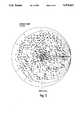
- FIG. 5is a Smith chart detailing the performance achieved from testing a circuit with a solid state load according to this invention.
- a solid state load according to this inventionis detailed schematically in FIG. 1.
- the use of a single solid state diode array 20such as that shown in FIG. 2 allows for effective generation of a variety of impedances by altering the voltage states of given diodes in the array 20.
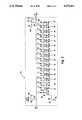
- This arraycomprises a series of diodes 1-15 and 46 interconnected to each other and having grounded capacitors 16-30 and 84 and an RF bypass network that includes respective shunt capacitors 84-99 and RF coils 68-83. All of the aforementioned array elements can be formed as part of a single semi-conductor wafer structure.
- Each diodeis driven by applying a predetermined voltage to its respective input 52-67. In this embodiment of bias voltage of approximately 50 volts is preferred.
- a DC bias currentcan be provided to the array at connection point 48 along the array via point 106 and RF bypass network 49 which includes RF coil 50 and shunt capacitor 51.
- the control circuitry for driving the diodescan be similar to that of above-described U.S. Pat. No. 5,034,708, except that the inputs 52-67 are driven fully on or off by the circuitry.
- Capacitors 100 and 101can be placed at opposite ends of the array to prevent the DC bias current from exiting the array.
- RF coil 104 with shunt capacitor 105comprise another RF bypass to prevent the input RF from interacting with the DC bias source.
- the array 20comprises a number of diodes substantially directly connected to each other.
- the diode arraycan also comprise diodes separated by predetermined lengths of connector media, such as microstrip transmission line.
- the physical lengths of the transmission linecan be varied according to a numerical formula such as a prime number relationship or can be equal in length.
- an array of diodes as shown in FIG. 2, comprising, for example, as PIN diodes,is not generally capable of handling power of more than approximately 7 Watts. Accordingly, the active load pull approach offered by a diode array has heretofore been unavailable for high power testing applications. Rather, less effective mechanical tuners have been utilized for high power applications.
- This inventionovercomes the disadvantages of a single diode array by providing a plurality of arrays linked by a combiner network. In this manner, a phase shift between the two arrays is effected to square the number of possible impedances.
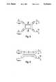
- two diode arrays 20(a) and 20(b) of the type shown in FIG. 2are connected via their RF inputs (RF IN) to each of two ports 110 and 112 of a combiner network 24.
- PORT 1 of the combiner network 24comprises an input port while PORT 2 comprises an output port.
- the arrays 20(a) and 20(b)are identical in this example and are connected to each of the two intermediate ports of the combiner network.
- the RF output of each arraycomprises an open circuit 25 in this example.
- the impedance presented at PORT 1can be characterized by the following equation in which Z 1 is the impedance of the first diode array and Z 2 is the impedance of the second diode array:
- the total number of impedances available for a pair of arrays having diodes driven either fully on or fully offis the square of the number of diodes plus one in each of the diode arrays. For example, in a circuit having a pair of 24 diode arrays, the total number of impedance states equals 625. Thus, a fairly large number of high power handling impedances can be provided to a load according to FIG. 1.
- the combiner network 24 of the preferred embodimentcomprises any one of a number of known hybrid circuits.
- FIGS. 3 and 4illustrate two possible alternative embodiments for a combiner network 24 according to this invention
- FIG. 3represents a branch-line quadrature hybrid in microstrip or stripline form. This hybrid is also known as a 90° hybrid.
- Each of the branches in this hybridare 1/4 wavelength ( ⁇ /4) in length and characterized by resistance R.
- PORT 1 and PORT 2are clearly illustrated.
- FIG. 4illustrates schematically an alternative combiner network comprising a coupled-line hybrid of a conventional type.
- a preferred combiner network according to this inventioncomprises a 90° or quadrature hybrid as shown in FIG. 3.
- a 90° hybridis preferred due to its low combining loss and equal signal split over multiple octave bandwidths.
- an input at PORT 1has a 0° phase change at the first array 20(a) signal at 110 and a 3 decibels reduction in power.
- the signal at 112 at the second array 20(b)is 90° out of phase with the input at PORT 1 and reduced by 3 decibels relative to the PORT 1 input signal.
- the signal at PORT 2should optimally remain in phase with that of PORT 1.
- any variation in phasecan be eliminated by adjusting the relative impedance of each of the first and second diode arrays 20(a) and 20(b).
- FIG. 5the performance of the solid state load according to this invention is depicted graphically in the form of a Smith chart.
- Each of the pointsrepresents a reflection coefficient of the load.
- the measurements hereinwere made for a frequency range of 1-2 GHz. Note that a wide range and large field of reflection coefficients is obtained with the load according to this invention.
- this high power solid state loadrepresents a versatile and reliable device for performing measurements on microwave devices.
Landscapes
- Microwave Amplifiers (AREA)
Abstract
Description
Z.sub.port 1 =1/2×(Z.sub.1 e.sup.jπ +Z.sub.2 e.sup.j0)
Claims (2)
Priority Applications (1)
| Application Number | Priority Date | Filing Date | Title |
|---|---|---|---|
| US07/898,204US5276411A (en) | 1992-06-01 | 1992-06-01 | High power solid state programmable load |
Applications Claiming Priority (1)
| Application Number | Priority Date | Filing Date | Title |
|---|---|---|---|
| US07/898,204US5276411A (en) | 1992-06-01 | 1992-06-01 | High power solid state programmable load |
Publications (1)
| Publication Number | Publication Date |
|---|---|
| US5276411Atrue US5276411A (en) | 1994-01-04 |
Family
ID=25409098
Family Applications (1)
| Application Number | Title | Priority Date | Filing Date |
|---|---|---|---|
| US07/898,204Expired - LifetimeUS5276411A (en) | 1992-06-01 | 1992-06-01 | High power solid state programmable load |
Country Status (1)
| Country | Link |
|---|---|
| US (1) | US5276411A (en) |
Cited By (52)
| Publication number | Priority date | Publication date | Assignee | Title |
|---|---|---|---|---|
| US5572160A (en)* | 1994-12-01 | 1996-11-05 | Teradyne, Inc. | Architecture for RF signal automatic test equipment |
| US5587934A (en)* | 1993-10-21 | 1996-12-24 | Wiltron Company | Automatic VNA calibration apparatus |
| US5670881A (en)* | 1996-02-09 | 1997-09-23 | Toshiba America, Inc. | Discrete step remotely adjustable matching circuit for MRI RF coils |
| US5715183A (en)* | 1994-12-07 | 1998-02-03 | Wiltron Company | Internal automatic calibrator for vector network analyzers |
| US6249128B1 (en) | 1997-10-22 | 2001-06-19 | Teradyne, Inc. | Automated microwave test system with improved accuracy |
| US6297649B1 (en) | 1999-09-30 | 2001-10-02 | Focus Microwaves Inc. | Harmonic rejection load tuner |
| EP1296149A1 (en)* | 2001-09-24 | 2003-03-26 | Agilent Technologies, Inc. (a Delaware corporation) | Characterizing non-linear behavior |
| US20030234708A1 (en)* | 2002-06-24 | 2003-12-25 | Pellegrini Massimo M. | RF switch including diodes with instrinsic regions |
| US20040085136A1 (en)* | 2002-10-30 | 2004-05-06 | Agilent Technologies, Inc. | Providing controllable impedance at a reference plane in a circuit |
| WO2004113936A1 (en)* | 2003-06-04 | 2004-12-29 | Technische Universiteit Delft | Loss-compensating circuit |
| RU2355102C1 (en)* | 2007-11-06 | 2009-05-10 | ВОЕННАЯ АКАДЕМИЯ СВЯЗИ имени С.М. Буденного Министерство Обороны Российской Федерации | Discrete reactive circuit (versions) |
| RU2414809C1 (en)* | 2010-04-06 | 2011-03-20 | Государственное образовательное учреждение высшего профессионального образования "Военная академия связи имени С.М. Буденного" Министерства обороны Российской Федерации | Discrete reaction circuit |
| US8610499B2 (en) | 2011-04-11 | 2013-12-17 | Auriga Measurement Systems, LLC | Radio frequency (RF) amplifier utilizing a predistortion circuit and related techniques |
| WO2014194256A1 (en) | 2013-05-31 | 2014-12-04 | Maury Microwave, Inc. | Solid state impedance tuners |
| EP2950449A1 (en)* | 2014-05-28 | 2015-12-02 | Alcatel Lucent | Attenuator |
| US9213056B1 (en) | 2013-05-29 | 2015-12-15 | Christos Tsironis | Multi-source active injection load pull system and method |
| EP2996190A1 (en)* | 2014-09-09 | 2016-03-16 | Alcatel Lucent | Method for selecting a phase shift, phase shifter, beamformer and antenna array |
| US20160172737A1 (en)* | 2014-12-10 | 2016-06-16 | Skyworks Solutions, Inc. | Rf coupler with decoupled state |
| US9431999B1 (en) | 2014-02-17 | 2016-08-30 | Christos Tsironis | Intelligent mechanical balancing apparatus for slide screw tuners |
| US9748627B2 (en) | 2014-06-12 | 2017-08-29 | Skyworks Solutions, Inc. | Devices and methods related to directional couplers |
| US9755670B2 (en) | 2014-05-29 | 2017-09-05 | Skyworks Solutions, Inc. | Adaptive load for coupler in broadband multimode multiband front end module |
| US9857410B1 (en) | 2015-11-02 | 2018-01-02 | Christos Tsironis | Tuning method for hybrid active injection load pull system |
| US9866244B2 (en) | 2015-09-10 | 2018-01-09 | Skyworks Solutions, Inc. | Electromagnetic couplers for multi-frequency power detection |
| US9900060B1 (en) | 2015-05-12 | 2018-02-20 | Superlative Semiconductor, LLC | Tunable microwave network and application to transmit leakage cancellation circuit in an RFID interrogator |
| US9941856B2 (en) | 2014-07-24 | 2018-04-10 | Skyworks Solutions, Inc. | Apparatus for reconfigurable directional couplers in an RF transceiver with selectable phase shifters |
| US9953938B2 (en) | 2016-03-30 | 2018-04-24 | Skyworks Solutions, Inc. | Tunable active silicon for coupler linearity improvement and reconfiguration |
| US9954564B2 (en) | 2016-02-05 | 2018-04-24 | Skyworks Solutions, Inc. | Electromagnetic couplers with multi-band filtering |
| US9960747B2 (en) | 2016-02-29 | 2018-05-01 | Skyworks Solutions, Inc. | Integrated filter and directional coupler assemblies |
| US10084224B2 (en) | 2016-04-29 | 2018-09-25 | Skyworks Solutions, Inc. | Compensated electromagnetic coupler |
| US10164681B2 (en) | 2016-06-06 | 2018-12-25 | Skyworks Solutions, Inc. | Isolating noise sources and coupling fields in RF chips |
| CN109274351A (en)* | 2018-08-14 | 2019-01-25 | 宁波大学 | Electronic impedance tuner |
| US10249930B2 (en) | 2016-04-29 | 2019-04-02 | Skyworks Solutions, Inc. | Tunable electromagnetic coupler and modules and devices using same |
| US10284167B2 (en) | 2016-05-09 | 2019-05-07 | Skyworks Solutions, Inc. | Self-adjusting electromagnetic coupler with automatic frequency detection |
| US10317445B1 (en)* | 2015-10-22 | 2019-06-11 | Christos Tsironis | High gamma electronic tuner |
| US10403955B2 (en) | 2016-06-22 | 2019-09-03 | Skyworks Solutions, Inc. | Electromagnetic coupler arrangements for multi-frequency power detection, and devices including same |
| US10742189B2 (en) | 2017-06-06 | 2020-08-11 | Skyworks Solutions, Inc. | Switched multi-coupler apparatus and modules and devices using same |
| US10972150B2 (en) | 2017-12-04 | 2021-04-06 | Superlative Semiconductor, LLC | Low-cost software-defined RFID interrogator with active transmit leakage cancellation |
| US11038249B1 (en) | 2018-11-29 | 2021-06-15 | Christos Tsironis | Harmonic hybrid electronic load pull tuner |
| US11119136B1 (en) | 2019-06-19 | 2021-09-14 | Christos Tsironis | Multi-octave hybrid harmonic load pull tuner |
| US11119140B1 (en) | 2017-08-31 | 2021-09-14 | Christos Tsironis | Impedance pattern generation for noise parameter measurement system |
| US11137439B1 (en) | 2018-08-20 | 2021-10-05 | Christos Tsironis | Hybrid load and source tuner using digital active loop |
| US11137430B1 (en) | 2018-06-28 | 2021-10-05 | Christos Tsironis | Active load pull tuning system for modulated signal |
| US11193966B1 (en) | 2020-04-03 | 2021-12-07 | Christos Tsironis | Low frequency active load pull tuner |
| US11217870B1 (en) | 2020-04-03 | 2022-01-04 | Christos Tsironis | Digital load pull tuner |
| US11391770B1 (en) | 2019-05-21 | 2022-07-19 | Christos Tsironis | Heterodyne active electronic load pull tuner |
| US11431379B1 (en)* | 2021-03-31 | 2022-08-30 | Teradyne, Inc. | Front-end module |
| US11480610B1 (en) | 2020-12-01 | 2022-10-25 | Christos Tsironis | Load pull pattern generation |
| US11728788B1 (en) | 2020-04-02 | 2023-08-15 | Christos Tsironis | Tuning methods for digital hybrid load pull system |
| US11863148B1 (en)* | 2021-07-15 | 2024-01-02 | Christos Tsironis | Active impedance tuner for base-band load pull |
| US11867736B1 (en)* | 2021-10-29 | 2024-01-09 | Christos Tsironis | Load pull system using waveguide tuner |
| US12057611B2 (en) | 2021-06-02 | 2024-08-06 | Skyworks Solutions, Inc. | Directional coupler with multiple arrangements of termination |
| US12142809B2 (en) | 2021-02-23 | 2024-11-12 | Skyworks Solutions, Inc. | Bidirectional RF coupler with switchable coupled transmission lines for operation over different frequency bands |
Citations (7)
| Publication number | Priority date | Publication date | Assignee | Title |
|---|---|---|---|---|
| US3454906A (en)* | 1967-05-02 | 1969-07-08 | Texas Instruments Inc | Bisected diode loaded line phase shifter |
| US3559108A (en)* | 1969-08-21 | 1971-01-26 | Bell Telephone Labor Inc | Coupler switches |
| US4450419A (en)* | 1982-09-29 | 1984-05-22 | Rca Corporation | Monolithic reflection phase shifter |
| US4764740A (en)* | 1987-08-10 | 1988-08-16 | Micronav Ltd. | Phase shifter |
| US4939485A (en)* | 1988-12-09 | 1990-07-03 | Varian Associates, Inc. | Microwave field effect switch |
| US5034708A (en)* | 1989-05-16 | 1991-07-23 | Automatic Testing And Networking, Inc. | Programmable broadband electronic tuner |
| US5109204A (en)* | 1990-12-03 | 1992-04-28 | Honeywell Inc. | High power RF precision attenuator |
- 1992
- 1992-06-01USUS07/898,204patent/US5276411A/ennot_activeExpired - Lifetime
Patent Citations (7)
| Publication number | Priority date | Publication date | Assignee | Title |
|---|---|---|---|---|
| US3454906A (en)* | 1967-05-02 | 1969-07-08 | Texas Instruments Inc | Bisected diode loaded line phase shifter |
| US3559108A (en)* | 1969-08-21 | 1971-01-26 | Bell Telephone Labor Inc | Coupler switches |
| US4450419A (en)* | 1982-09-29 | 1984-05-22 | Rca Corporation | Monolithic reflection phase shifter |
| US4764740A (en)* | 1987-08-10 | 1988-08-16 | Micronav Ltd. | Phase shifter |
| US4939485A (en)* | 1988-12-09 | 1990-07-03 | Varian Associates, Inc. | Microwave field effect switch |
| US5034708A (en)* | 1989-05-16 | 1991-07-23 | Automatic Testing And Networking, Inc. | Programmable broadband electronic tuner |
| US5109204A (en)* | 1990-12-03 | 1992-04-28 | Honeywell Inc. | High power RF precision attenuator |
Non-Patent Citations (6)
| Title |
|---|
| Adamian, V., "Stable Source Aids Automated Noise-Parameter Measurements", The Time and Measurement Notebook, Feb., 1988, pp. 51-58. |
| Adamian, V., Stable Source Aids Automated Noise Parameter Measurements , The Time and Measurement Notebook, Feb., 1988, pp. 51 58.* |
| Froelich R., "Automated Tuning for Noise Parameter Measurements Using a Microwave Probe", Watkins-Johnson Co., Mar. 1989, pp. 83-96. |
| Froelich R., Automated Tuning for Noise Parameter Measurements Using a Microwave Probe , Watkins Johnson Co., Mar. 1989, pp. 83 96.* |
| Froelich, R., "Measurement of GaAs FET Noise Parameters", Watkins-Johnson Co., vol. 13, No. 6, Nov./Dec. 86, pp. 2-11. |
| Froelich, R., Measurement of GaAs FET Noise Parameters , Watkins Johnson Co., vol. 13, No. 6, Nov./Dec. 86, pp. 2 11.* |
Cited By (73)
| Publication number | Priority date | Publication date | Assignee | Title |
|---|---|---|---|---|
| US5587934A (en)* | 1993-10-21 | 1996-12-24 | Wiltron Company | Automatic VNA calibration apparatus |
| US5572160A (en)* | 1994-12-01 | 1996-11-05 | Teradyne, Inc. | Architecture for RF signal automatic test equipment |
| EP0715177A3 (en)* | 1994-12-01 | 1997-05-07 | Teradyne Inc | Architecture for RF signal automatic test equipment |
| US6066953A (en)* | 1994-12-01 | 2000-05-23 | Teradyne, Inc. | Architecture for RF signal automatic test equipment |
| US5715183A (en)* | 1994-12-07 | 1998-02-03 | Wiltron Company | Internal automatic calibrator for vector network analyzers |
| US5670881A (en)* | 1996-02-09 | 1997-09-23 | Toshiba America, Inc. | Discrete step remotely adjustable matching circuit for MRI RF coils |
| US6249128B1 (en) | 1997-10-22 | 2001-06-19 | Teradyne, Inc. | Automated microwave test system with improved accuracy |
| US6297649B1 (en) | 1999-09-30 | 2001-10-02 | Focus Microwaves Inc. | Harmonic rejection load tuner |
| US6839657B2 (en) | 2001-09-24 | 2005-01-04 | Agilent Technologies, Inc. | Method of and an arrangement for characterizing non-linear behavior of RF and microwave devices in a near matched environment |
| EP1296149A1 (en)* | 2001-09-24 | 2003-03-26 | Agilent Technologies, Inc. (a Delaware corporation) | Characterizing non-linear behavior |
| US20030234708A1 (en)* | 2002-06-24 | 2003-12-25 | Pellegrini Massimo M. | RF switch including diodes with instrinsic regions |
| US6967547B2 (en)* | 2002-06-24 | 2005-11-22 | Signal Technology Corporation | RF switch including diodes with intrinsic regions |
| US20040085136A1 (en)* | 2002-10-30 | 2004-05-06 | Agilent Technologies, Inc. | Providing controllable impedance at a reference plane in a circuit |
| US6930564B2 (en) | 2002-10-30 | 2005-08-16 | Agilent Technologies, Inc. | Providing controllable impedance at a reference plane in a circuit |
| WO2004113936A1 (en)* | 2003-06-04 | 2004-12-29 | Technische Universiteit Delft | Loss-compensating circuit |
| RU2355102C1 (en)* | 2007-11-06 | 2009-05-10 | ВОЕННАЯ АКАДЕМИЯ СВЯЗИ имени С.М. Буденного Министерство Обороны Российской Федерации | Discrete reactive circuit (versions) |
| RU2414809C1 (en)* | 2010-04-06 | 2011-03-20 | Государственное образовательное учреждение высшего профессионального образования "Военная академия связи имени С.М. Буденного" Министерства обороны Российской Федерации | Discrete reaction circuit |
| US8610499B2 (en) | 2011-04-11 | 2013-12-17 | Auriga Measurement Systems, LLC | Radio frequency (RF) amplifier utilizing a predistortion circuit and related techniques |
| US9213056B1 (en) | 2013-05-29 | 2015-12-15 | Christos Tsironis | Multi-source active injection load pull system and method |
| WO2014194256A1 (en) | 2013-05-31 | 2014-12-04 | Maury Microwave, Inc. | Solid state impedance tuners |
| CN105264398A (en)* | 2013-05-31 | 2016-01-20 | 莫里微波公司 | Solid state impedance tuners |
| US9660607B2 (en) | 2013-05-31 | 2017-05-23 | Maury Microwave, Inc. | Solid state impedance tuners |
| US9431999B1 (en) | 2014-02-17 | 2016-08-30 | Christos Tsironis | Intelligent mechanical balancing apparatus for slide screw tuners |
| EP2950449A1 (en)* | 2014-05-28 | 2015-12-02 | Alcatel Lucent | Attenuator |
| US9755670B2 (en) | 2014-05-29 | 2017-09-05 | Skyworks Solutions, Inc. | Adaptive load for coupler in broadband multimode multiband front end module |
| US10128558B2 (en) | 2014-06-12 | 2018-11-13 | Skyworks Solutions, Inc. | Directional couplers and devices including same |
| US9748627B2 (en) | 2014-06-12 | 2017-08-29 | Skyworks Solutions, Inc. | Devices and methods related to directional couplers |
| US9948271B2 (en) | 2014-07-24 | 2018-04-17 | Skyworks Solutions, Inc. | Methods for reconfiguring directional couplers in an RF transceiver |
| US9941856B2 (en) | 2014-07-24 | 2018-04-10 | Skyworks Solutions, Inc. | Apparatus for reconfigurable directional couplers in an RF transceiver with selectable phase shifters |
| US9960750B2 (en) | 2014-07-24 | 2018-05-01 | Skyworks Solutions, Inc. | Apparatus for reconfigurable directional couplers in an RF transceiver with controllable capacitive coupling |
| EP2996190A1 (en)* | 2014-09-09 | 2016-03-16 | Alcatel Lucent | Method for selecting a phase shift, phase shifter, beamformer and antenna array |
| US9614269B2 (en)* | 2014-12-10 | 2017-04-04 | Skyworks Solutions, Inc. | RF coupler with adjustable termination impedance |
| US20160172738A1 (en)* | 2014-12-10 | 2016-06-16 | Skyworks Solutions, Inc. | Rf coupler with adjustable termination impedance |
| US9793592B2 (en)* | 2014-12-10 | 2017-10-17 | Skyworks Solutions, Inc. | RF coupler with decoupled state |
| US9812757B2 (en) | 2014-12-10 | 2017-11-07 | Skyworks Solutions, Inc. | RF coupler having coupled line with adjustable length |
| US20160172737A1 (en)* | 2014-12-10 | 2016-06-16 | Skyworks Solutions, Inc. | Rf coupler with decoupled state |
| US10187120B1 (en) | 2015-05-12 | 2019-01-22 | Superlative Semiconductor, LLC | Tunable microwave network and application to transmit leakage cancellation circuit in an RFID interrogator |
| US9900060B1 (en) | 2015-05-12 | 2018-02-20 | Superlative Semiconductor, LLC | Tunable microwave network and application to transmit leakage cancellation circuit in an RFID interrogator |
| US9866244B2 (en) | 2015-09-10 | 2018-01-09 | Skyworks Solutions, Inc. | Electromagnetic couplers for multi-frequency power detection |
| US10317445B1 (en)* | 2015-10-22 | 2019-06-11 | Christos Tsironis | High gamma electronic tuner |
| US9857410B1 (en) | 2015-11-02 | 2018-01-02 | Christos Tsironis | Tuning method for hybrid active injection load pull system |
| US9954564B2 (en) | 2016-02-05 | 2018-04-24 | Skyworks Solutions, Inc. | Electromagnetic couplers with multi-band filtering |
| US9960747B2 (en) | 2016-02-29 | 2018-05-01 | Skyworks Solutions, Inc. | Integrated filter and directional coupler assemblies |
| US9953938B2 (en) | 2016-03-30 | 2018-04-24 | Skyworks Solutions, Inc. | Tunable active silicon for coupler linearity improvement and reconfiguration |
| US10553925B2 (en) | 2016-04-29 | 2020-02-04 | Skyworks Solutions, Inc. | Tunable electromagnetic coupler and modules and devices using same |
| US10084224B2 (en) | 2016-04-29 | 2018-09-25 | Skyworks Solutions, Inc. | Compensated electromagnetic coupler |
| US10249930B2 (en) | 2016-04-29 | 2019-04-02 | Skyworks Solutions, Inc. | Tunable electromagnetic coupler and modules and devices using same |
| US10284167B2 (en) | 2016-05-09 | 2019-05-07 | Skyworks Solutions, Inc. | Self-adjusting electromagnetic coupler with automatic frequency detection |
| US10707826B2 (en) | 2016-05-09 | 2020-07-07 | Skyworks Solutions, Inc. | Self-adjusting electromagnetic coupler with automatic frequency detection |
| US10164681B2 (en) | 2016-06-06 | 2018-12-25 | Skyworks Solutions, Inc. | Isolating noise sources and coupling fields in RF chips |
| US10763568B2 (en) | 2016-06-22 | 2020-09-01 | Skyworks Solutions, Inc. | Electromagnetic coupler arrangements for multi-frequency power detection, and devices including same |
| US10403955B2 (en) | 2016-06-22 | 2019-09-03 | Skyworks Solutions, Inc. | Electromagnetic coupler arrangements for multi-frequency power detection, and devices including same |
| US10742189B2 (en) | 2017-06-06 | 2020-08-11 | Skyworks Solutions, Inc. | Switched multi-coupler apparatus and modules and devices using same |
| US11119140B1 (en) | 2017-08-31 | 2021-09-14 | Christos Tsironis | Impedance pattern generation for noise parameter measurement system |
| US10972150B2 (en) | 2017-12-04 | 2021-04-06 | Superlative Semiconductor, LLC | Low-cost software-defined RFID interrogator with active transmit leakage cancellation |
| US11137430B1 (en) | 2018-06-28 | 2021-10-05 | Christos Tsironis | Active load pull tuning system for modulated signal |
| US10566953B1 (en) | 2018-08-14 | 2020-02-18 | Ningbo University | Electronic impedance tuner |
| CN109274351A (en)* | 2018-08-14 | 2019-01-25 | 宁波大学 | Electronic impedance tuner |
| CN109274351B (en)* | 2018-08-14 | 2022-03-29 | 宁波大学 | An electronic impedance tuner |
| US11137439B1 (en) | 2018-08-20 | 2021-10-05 | Christos Tsironis | Hybrid load and source tuner using digital active loop |
| US11038249B1 (en) | 2018-11-29 | 2021-06-15 | Christos Tsironis | Harmonic hybrid electronic load pull tuner |
| US11391770B1 (en) | 2019-05-21 | 2022-07-19 | Christos Tsironis | Heterodyne active electronic load pull tuner |
| US11119136B1 (en) | 2019-06-19 | 2021-09-14 | Christos Tsironis | Multi-octave hybrid harmonic load pull tuner |
| US11863163B1 (en) | 2020-04-02 | 2024-01-02 | Christos Tsironis | Digital hybrid load pull system |
| US11728788B1 (en) | 2020-04-02 | 2023-08-15 | Christos Tsironis | Tuning methods for digital hybrid load pull system |
| US11217870B1 (en) | 2020-04-03 | 2022-01-04 | Christos Tsironis | Digital load pull tuner |
| US11193966B1 (en) | 2020-04-03 | 2021-12-07 | Christos Tsironis | Low frequency active load pull tuner |
| US11480610B1 (en) | 2020-12-01 | 2022-10-25 | Christos Tsironis | Load pull pattern generation |
| US12142809B2 (en) | 2021-02-23 | 2024-11-12 | Skyworks Solutions, Inc. | Bidirectional RF coupler with switchable coupled transmission lines for operation over different frequency bands |
| US11431379B1 (en)* | 2021-03-31 | 2022-08-30 | Teradyne, Inc. | Front-end module |
| US12057611B2 (en) | 2021-06-02 | 2024-08-06 | Skyworks Solutions, Inc. | Directional coupler with multiple arrangements of termination |
| US11863148B1 (en)* | 2021-07-15 | 2024-01-02 | Christos Tsironis | Active impedance tuner for base-band load pull |
| US11867736B1 (en)* | 2021-10-29 | 2024-01-09 | Christos Tsironis | Load pull system using waveguide tuner |
Similar Documents
| Publication | Publication Date | Title |
|---|---|---|
| US5276411A (en) | High power solid state programmable load | |
| US4502028A (en) | Programmable two-port microwave network | |
| EP0849820B1 (en) | Tunable microwave network using microelectromechanical switches | |
| US5034708A (en) | Programmable broadband electronic tuner | |
| EP0547615A1 (en) | Line-loop diode phase bit circuit | |
| US5634208A (en) | Multilayer transmission line using ground metal with slit, and hybrid using the transmission line | |
| EP1713144A1 (en) | Quadrature hybrid circuit | |
| US5119050A (en) | Low loss 360 degree x-band analog phase shifter | |
| US6320480B1 (en) | Wideband low-loss variable delay line and phase shifter | |
| US5109204A (en) | High power RF precision attenuator | |
| US4977382A (en) | Vector modulator phase shifter | |
| US8125302B2 (en) | Signal selecting device | |
| CN117938116A (en) | A digitally controlled attenuator with slope control | |
| US4823096A (en) | Variable ratio power divider/combiner | |
| Coats | An octave-band switched-line microstrip 3-b diode phase shifter | |
| US5521560A (en) | Minimum phase shift microwave attenuator | |
| US4288763A (en) | Analog phase shifter | |
| US4760350A (en) | Internally matched power amplifier | |
| KR20240135757A (en) | Cascaded low-noise wideband active phase shifter | |
| Mikucki et al. | A broad-band printed circuit hybrid ring power divider | |
| US4346315A (en) | Switched delay line for steerable null antenna system | |
| CN100508367C (en) | Amplifier with wide output power dynamic range | |
| US5477200A (en) | Variable attenuator | |
| CN110459838B (en) | Phase shifter, phased array antenna apparatus, and phase shifting method | |
| KR20210140770A (en) | Power distributor, regulation method, power distribution method, storage medium and electronic device |
Legal Events
| Date | Code | Title | Description |
|---|---|---|---|
| AS | Assignment | Owner name:ATN MICROWAVE, INC., MASSACHUSETTS Free format text:ASSIGNMENT OF ASSIGNORS INTEREST.;ASSIGNORS:WOODIN, CHARLES E., JR.;WANDREI, DAVID L.;REEL/FRAME:006256/0559 Effective date:19920811 | |
| FEPP | Fee payment procedure | Free format text:PAYOR NUMBER ASSIGNED (ORIGINAL EVENT CODE: ASPN); ENTITY STATUS OF PATENT OWNER: LARGE ENTITY | |
| STCF | Information on status: patent grant | Free format text:PATENTED CASE | |
| FPAY | Fee payment | Year of fee payment:4 | |
| FEPP | Fee payment procedure | Free format text:PAYOR NUMBER ASSIGNED (ORIGINAL EVENT CODE: ASPN); ENTITY STATUS OF PATENT OWNER: LARGE ENTITY Free format text:PAYER NUMBER DE-ASSIGNED (ORIGINAL EVENT CODE: RMPN); ENTITY STATUS OF PATENT OWNER: LARGE ENTITY | |
| FEPP | Fee payment procedure | Free format text:PAYER NUMBER DE-ASSIGNED (ORIGINAL EVENT CODE: RMPN); ENTITY STATUS OF PATENT OWNER: LARGE ENTITY Free format text:PAYOR NUMBER ASSIGNED (ORIGINAL EVENT CODE: ASPN); ENTITY STATUS OF PATENT OWNER: LARGE ENTITY | |
| FEPP | Fee payment procedure | Free format text:PAT HLDR NO LONGER CLAIMS SMALL ENT STAT AS SMALL BUSINESS (ORIGINAL EVENT CODE: LSM2); ENTITY STATUS OF PATENT OWNER: LARGE ENTITY | |
| AS | Assignment | Owner name:AGILENT TECHNOLOGIES, INC., CALIFORNIA Free format text:ASSIGNMENT OF ASSIGNORS INTEREST;ASSIGNOR:ATN MICROWAVE, INC.;REEL/FRAME:011679/0542 Effective date:20010613 | |
| FPAY | Fee payment | Year of fee payment:8 | |
| FPAY | Fee payment | Year of fee payment:12 |