US5272485A - Microstrip antenna with integral low-noise amplifier for use in global positioning system (GPS) receivers - Google Patents
Microstrip antenna with integral low-noise amplifier for use in global positioning system (GPS) receiversDownload PDFInfo
- Publication number
- US5272485A US5272485AUS07/830,738US83073892AUS5272485AUS 5272485 AUS5272485 AUS 5272485AUS 83073892 AUS83073892 AUS 83073892AUS 5272485 AUS5272485 AUS 5272485A
- Authority
- US
- United States
- Prior art keywords
- antenna
- transistor
- groundplane
- electrode
- dielectric substrate
- Prior art date
- Legal status (The legal status is an assumption and is not a legal conclusion. Google has not performed a legal analysis and makes no representation as to the accuracy of the status listed.)
- Expired - Fee Related
Links
Images
Classifications
- H—ELECTRICITY
- H01—ELECTRIC ELEMENTS
- H01Q—ANTENNAS, i.e. RADIO AERIALS
- H01Q1/00—Details of, or arrangements associated with, antennas
- H01Q1/27—Adaptation for use in or on movable bodies
- H01Q1/32—Adaptation for use in or on road or rail vehicles
- H01Q1/325—Adaptation for use in or on road or rail vehicles characterised by the location of the antenna on the vehicle
- H01Q1/3275—Adaptation for use in or on road or rail vehicles characterised by the location of the antenna on the vehicle mounted on a horizontal surface of the vehicle, e.g. on roof, hood, trunk
- H—ELECTRICITY
- H01—ELECTRIC ELEMENTS
- H01Q—ANTENNAS, i.e. RADIO AERIALS
- H01Q23/00—Antennas with active circuits or circuit elements integrated within them or attached to them
- H—ELECTRICITY
- H01—ELECTRIC ELEMENTS
- H01Q—ANTENNAS, i.e. RADIO AERIALS
- H01Q9/00—Electrically-short antennas having dimensions not more than twice the operating wavelength and consisting of conductive active radiating elements
- H01Q9/04—Resonant antennas
- H01Q9/0407—Substantially flat resonant element parallel to ground plane, e.g. patch antenna
Definitions
- the inventionrelates generally to diagonally fed electric microstrip dipole antennas and specifically to such antennas where the feedpoint and via inductance are used to provide a low noise amplifier with the optimum impedance for minimum noise figure ( ⁇ b).
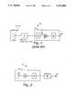
- FIG. 1shows a conventional system 10 with a Global Positioning System (GPS) antenna 12, a cable 14, and a low-noise amplifier (LNA) 16 in a typical configuration where the coaxial cable 14 (with a loss equal to Lc) links microstrip antenna 12 (with a feedpoint and via inductance having an optimum noise figure source impedance ( ⁇ s) equal to zero) to the LNA 16 having an input loss (Linput of Lc+L imn ).
- a fifty ohm matchis made possible by an input matching network (IMN) 18 which drives an active device 20 and an output match network (OMN) 22.
- INNinput matching network
- OPNoutput match network
- a diagonally fed electric microstrip antennais described by Kaloi in U.S. Pat. No. 3,984,834, issued Oct. 5, 1976.
- the feedpointis located along a diagonal with respect to the rectangular antenna element on a dielectric substrate.
- This particular point of feedis said by Kaloi to cause the antenna to operate in a degenerate mode where two oscillations occur at the same frequency. These oscillations occur along the X axis and the Y axis.
- the respective axis dimensionsdetermine the resonant frequencies of each. Design equations for this type of antenna are presented by Kaloi, and so are not repeated here.
- the feedpoint of a diagonally fed electric microstrip antennacan be chosen to present a particular impedance, for example fifty ohms. However, such a point may not be the point that produces a minimum of noise. Therefore, a diagonally fed electric microstrip antenna with a minimum noise feedpoint and an integrated LNA is needed to permit the reliable operation of high performance systems, such as personal, hand-held GPS receivers.
- an embodiment of the present inventionis a diagonally fed electric microstrip antenna having a ceramic substrate, a groundplane on one side of the substrate, a rectangularly-shaped radiator attached to the other side of the substrate, and a via that passes through the substrate and connects to a point on the radiating electrode that provides a predetermined impedance Z o , the via has an inductance L via such that an optimum impedance for a minimum noise figure ⁇ o is presented to the opposite end of the via.
- a groundplane relief on the first side of the dielectric substrateallows an active device to be connected to the second end of the via and placed within the groundplane relief.
- An output matching network also inside the groundplane reliefis used for coupling the active device to an external system, such as a Global Positioning System (GPS) receiver.
- GPSGlobal Positioning System
- An advantage of the present inventionis that losses in an active device's input matching network are eliminated because the network itself is eliminated.
- Another advantage of the present inventionis that noise factor (NF) degradation due to cable loss is eliminated.
- NFnoise factor
- Another advantage of the present inventionis that the via to the feedpoint on a radiator provides the inductance needed to connect to the ⁇ o point of optimum low noise.
- FIG. 1is a block diagram of a prior art microstrip antenna connected through a cable to a low-noise amplifier;
- FIG. 2is a block diagram of microstrip antenna and an integrated low-noise amplifier, according to an embodiment of the present invention
- FIGS. 3A through 3Care a bottom, groundplane view; an edge view; and a top, radiator view, respectively, of a microstrip antenna, according to an embodiment of the present invention
- FIGS. 4A and 4Bare a bottom, groundplane view and an edge view, respectively, of the microstrip antenna and integrated low-noise amplifier of FIG. 2;
- FIGS. 5A and 5Bare block diagrams of two examples of a filtered pre-amplifier, according to the present invention.
- FIG. 6is a bottom, groundplane view of an antenna pre-amplifier with the filter of FIGS. 5A;
- FIG. 7is an edge view of the pre-amplifier of FIGS. 5A and 6 with shields attached.
- a system 40comprises an integrated assembly 42 having a microstrip antenna 43, an active device 44, and an output matching network 45.
- a cable 46couples assembly 42 to an external system at port 48.
- the connection between antenna 43 and active device 44is at a point of predetermined impedance Z o , the connection has an inductance L via such that an optimum impedance for a minimum noise figure ⁇ o is present at the input of active device 44.
- a GaAs FET transistorcan be used for active device 45. Other high-gain, low-noise transistors can also be used with good results.
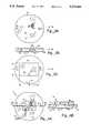
- FIGS. 3A-3Cshow a second embodiment of the present invention, which is a microstrip antenna 50 comprising a ceramic substrate 52, a first metal layer 54 that completely covers one side of microstrip antenna 50 except for an opening 56 which encircles a metal annular ring 58 in contact with a plated-through hole (via) 60.
- Microstrip antenna 50further comprises a second metal layer 62 having a rectangular shape of dimensions "A" by "B” and that is tapped by via 60.
- a hole 64 and a slot 66allow microstrip antenna 50 to be mounted to a surface with common fasteners.
- Microstrip antenna 50is generally a round disk in shape, but has a flat edge 68 for orientation.
- the first metal layer 54is alternatively referred to herein as a groundplane and second metal layer 62 is alternatively referred to herein as a radiating element.
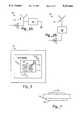
- a third embodiment of the present inventionis shown and is a pre-amplified antenna 70 comprising dielectric substrate 72, a groundplane 74, a radiator 76, an interconnect cable 78, a round mounting hole 80, an elongated mounting hole 82, a groundplane relief 84, a groundplane relief lid 86, and an active device 88.
- An output matching network (OMN) 90couples active device 88 to cable 78.
- a via 92couples active device 88 to a point of predetermined impedance Z o .
- Via 92has an inductance L via a such that an optimum impedance for a minimum noise figure ⁇ o is present at the input of active device 88.
- via 92is adjusted to modify the inductance and the X-Y coordinate point in radiator 76 is adjusted to modify the impedance Zo. Impedances of fifty ohms are common in the industry. Without the conductive attachment of conductive lid 86, the relief of groundplane relief 84 in groundplane 74 would lower the antenna resonant frequency. Lid 86 functions as an RF shield to eliminate positive feedback from the active device 88 through antenna 70 and it minimizes the detuning effects of the hole in groundplane 74 by restoring a more direct path for antenna ground current to flow.
- the third embodimentis described herein as a pre-amplifier, the general construction strategy shown here can be successfully employed to produce a high-performance transmitter antenna.
- the output of active device 88would drive via 92 and cable 78 is connected to a transmitter.
- FIGS. 5A and 5Ba pre-amplified antenna 100 is shown with a bandstop filter 102 in FIG. 5A and with a band-pass filter 104 in FIG. 5B.
- An active stage 106outputs received signals to an external receiver.
- the construction of antenna 100is similar to that of antenna 70.
- Groundplane relief 84is used to house filter 102 or 104, or both.
- FIG. 6shows an example of how a filter, such as filters 102 and 104 would be mounted in the groundplane relief of an antenna like antenna 100.
- the filterscan be Pi-network or T-network types, depending on the frequencies being filtered and the bandwidths (or "Q") required. Such filters are conventional, an example of which is described in U.S. Pat. No.
- a filteris fabricated from a planar dielectric substrate having a ground plane on one side and two thin-film metal layers and an insulation layer on the other side.
- the metal and insulation layersare configured to form one or more capacitive pi-networks and spiral inductors, and are electrically interconnected to form the filter.
- a via 110connects to a radiator (not shown) in the manner described above in the previous embodiments.
- Active stage 106can be located either inside the groundplane relief with the filter, or outside.
- FIG. 6shows only filter 102 within a groundplane relief 112, but filter 104 and/or active stage 106 could be located there as well, and with the advantages previously described.
- Outputis through a cable 114.
- a lid(not shown), which is similar to lid 86 (FIG. 4B), is preferably used to seal groundplane relief 112.
- FIG. 7shows how at least one shield 120 can be attached to an antenna, such as antenna 100, to shape the radio radiation pattern of antenna 100.
- the shield(s) 120can be either rectangular or circular in shape, depending on which one or which combination gives the best shape, according to a predetermined requirement.
- Shield(s) 120can act as radio wave directors and reflectors, depending on their geometry and the distance to the radiator (e.g., radiator 62.
- radiatore.g., radiator 62.
- isolated passive director elementsare made slightly shorter than the active elements, and tend to increase the radiation pattern lobe in the direction of the director and decrease it in the opposite direction.
- Reflector elementsare slightly longer than the active elements, and tend to decrease the radiation pattern lobe in the direction of the reflector and increase it in the opposite direction.
- Directors and reflectorscan be used simultaneously to produce, for example, highly directional patterns.
- the ratios of the X-Y dimensions in the dipole microstrip reflectors and directors (shields 120)need not repeat that of the main radiator (e.g., "A" and "B” for radiator 62). Manipulation of these respective dimensions can be done to achieve shapes that are different in the X and Y planes.
Landscapes
- Engineering & Computer Science (AREA)
- Remote Sensing (AREA)
- Waveguide Aerials (AREA)
- Variable-Direction Aerials And Aerial Arrays (AREA)
- Microwave Amplifiers (AREA)
Abstract
Description
1. Field of the Invention
The invention relates generally to diagonally fed electric microstrip dipole antennas and specifically to such antennas where the feedpoint and via inductance are used to provide a low noise amplifier with the optimum impedance for minimum noise figure (Γb).
2. Description of the Prior Art
FIG. 1 shows aconventional system 10 with a Global Positioning System (GPS)antenna 12, acable 14, and a low-noise amplifier (LNA) 16 in a typical configuration where the coaxial cable 14 (with a loss equal to Lc) links microstrip antenna 12 (with a feedpoint and via inductance having an optimum noise figure source impedance (Γs) equal to zero) to theLNA 16 having an input loss (Linput of Lc+Limn). A fifty ohm match is made possible by an input matching network (IMN) 18 which drives anactive device 20 and an output match network (OMN) 22. The noise figure (NF) contribution of the cable andIMN 18 is given by the available gain of thecable 14 andIMW 18.
The input loss of thecable 14 and IMN 18 add directly to the NF of the system Fsys. ##EQU1## where FROA =NF of the rest Of the GPS receiver following LNA 16.
As the present invention does, incorporatingLNA 16 inantenna 12 and repositioningcable 14 will reduce the system NF by the amount of input loss, if GLNA >>Lc LIMN, ##EQU2## The NF reduction is then,
F.sub.sys -F'.sub.sys =L.sub.c L.sub.IMN. (4)
A diagonally fed electric microstrip antenna is described by Kaloi in U.S. Pat. No. 3,984,834, issued Oct. 5, 1976. The feedpoint is located along a diagonal with respect to the rectangular antenna element on a dielectric substrate. This particular point of feed is said by Kaloi to cause the antenna to operate in a degenerate mode where two oscillations occur at the same frequency. These oscillations occur along the X axis and the Y axis. The respective axis dimensions determine the resonant frequencies of each. Design equations for this type of antenna are presented by Kaloi, and so are not repeated here.
The feedpoint of a diagonally fed electric microstrip antenna can be chosen to present a particular impedance, for example fifty ohms. However, such a point may not be the point that produces a minimum of noise. Therefore, a diagonally fed electric microstrip antenna with a minimum noise feedpoint and an integrated LNA is needed to permit the reliable operation of high performance systems, such as personal, hand-held GPS receivers.
It is therefore an object of the present invention to improve the reception of signals from GPS satellites.
Briefly, an embodiment of the present invention is a diagonally fed electric microstrip antenna having a ceramic substrate, a groundplane on one side of the substrate, a rectangularly-shaped radiator attached to the other side of the substrate, and a via that passes through the substrate and connects to a point on the radiating electrode that provides a predetermined impedance Zo, the via has an inductance Lvia such that an optimum impedance for a minimum noise figure Γo is presented to the opposite end of the via. A groundplane relief on the first side of the dielectric substrate allows an active device to be connected to the second end of the via and placed within the groundplane relief. An output matching network also inside the groundplane relief is used for coupling the active device to an external system, such as a Global Positioning System (GPS) receiver.
An advantage of the present invention is that losses in an active device's input matching network are eliminated because the network itself is eliminated.
Another advantage of the present invention is that noise factor (NF) degradation due to cable loss is eliminated.
Another advantage of the present invention is that the via to the feedpoint on a radiator provides the inductance needed to connect to the Γo point of optimum low noise.
These and other objects and advantages of the present invention will no doubt become obvious to those of ordinary skill in the art after having read the following detailed description of the preferred embodiments which are illustrated in the various drawing figures.
FIG. 1 is a block diagram of a prior art microstrip antenna connected through a cable to a low-noise amplifier;
FIG. 2 is a block diagram of microstrip antenna and an integrated low-noise amplifier, according to an embodiment of the present invention;
FIGS. 3A through 3C are a bottom, groundplane view; an edge view; and a top, radiator view, respectively, of a microstrip antenna, according to an embodiment of the present invention;
FIGS. 4A and 4B are a bottom, groundplane view and an edge view, respectively, of the microstrip antenna and integrated low-noise amplifier of FIG. 2; and
FIGS. 5A and 5B are block diagrams of two examples of a filtered pre-amplifier, according to the present invention;
FIG. 6 is a bottom, groundplane view of an antenna pre-amplifier with the filter of FIGS. 5A; and
FIG. 7 is an edge view of the pre-amplifier of FIGS. 5A and 6 with shields attached.
In FIG. 2, asystem 40, according to a first embodiment of the present invention, comprises an integratedassembly 42 having amicrostrip antenna 43, anactive device 44, and anoutput matching network 45. Acable 46couples assembly 42 to an external system atport 48. The external system can be a receiver, such as a GPS receiver, or a transmitter, in which caseactive device 44 would driveantenna 43 and ΓL =optimum load for maximum power. The connection betweenantenna 43 andactive device 44 is at a point of predetermined impedance Zo, the connection has an inductance Lvia such that an optimum impedance for a minimum noise figure Γo is present at the input ofactive device 44. A GaAs FET transistor can be used foractive device 45. Other high-gain, low-noise transistors can also be used with good results.
FIGS. 3A-3C show a second embodiment of the present invention, which is amicrostrip antenna 50 comprising aceramic substrate 52, afirst metal layer 54 that completely covers one side ofmicrostrip antenna 50 except for anopening 56 which encircles a metalannular ring 58 in contact with a plated-through hole (via) 60.Microstrip antenna 50 further comprises asecond metal layer 62 having a rectangular shape of dimensions "A" by "B" and that is tapped by via 60. Ahole 64 and aslot 66 allowmicrostrip antenna 50 to be mounted to a surface with common fasteners.Microstrip antenna 50 is generally a round disk in shape, but has aflat edge 68 for orientation. The dimensions "A" and "B", their ratio to one another, and the thickness and dielectric constant ofsubstrate 52 will determine the resonant frequency, and therefore the frequency of operation formicrostrip antenna 50. Such a determination, however, is conventional, and one skilled in the art will be able to pick a frequency of operation and to determine the appropriate dimensions "A" and "B".
Thefirst metal layer 54 is alternatively referred to herein as a groundplane andsecond metal layer 62 is alternatively referred to herein as a radiating element.
In FIGS. 4A and 4B, a third embodiment of the present invention is shown and is apre-amplified antenna 70 comprisingdielectric substrate 72, agroundplane 74, aradiator 76, aninterconnect cable 78, around mounting hole 80, anelongated mounting hole 82, agroundplane relief 84, agroundplane relief lid 86, and anactive device 88. An output matching network (OMN) 90 couplesactive device 88 tocable 78. A via 92 couplesactive device 88 to a point of predetermined impedance Zo. Via 92 has an inductance Lvia a such that an optimum impedance for a minimum noise figure Γo is present at the input ofactive device 88. The geometry ofvia 92 is adjusted to modify the inductance and the X-Y coordinate point inradiator 76 is adjusted to modify the impedance Zo. Impedances of fifty ohms are common in the industry. Without the conductive attachment ofconductive lid 86, the relief ofgroundplane relief 84 ingroundplane 74 would lower the antenna resonant frequency.Lid 86 functions as an RF shield to eliminate positive feedback from theactive device 88 throughantenna 70 and it minimizes the detuning effects of the hole ingroundplane 74 by restoring a more direct path for antenna ground current to flow.
Although the third embodiment is described herein as a pre-amplifier, the general construction strategy shown here can be successfully employed to produce a high-performance transmitter antenna. In such a case, the output ofactive device 88 would drive via 92 andcable 78 is connected to a transmitter.
In FIGS. 5A and 5B, apre-amplified antenna 100 is shown with abandstop filter 102 in FIG. 5A and with a band-pass filter 104 in FIG. 5B. Anactive stage 106 outputs received signals to an external receiver. The construction ofantenna 100 is similar to that ofantenna 70.Groundplane relief 84 is used tohouse filter filters antenna 100. The filters can be Pi-network or T-network types, depending on the frequencies being filtered and the bandwidths (or "Q") required. Such filters are conventional, an example of which is described in U.S. Pat. No. 4,881,050, issued Nov. 14, 1989 to Swanson, Jr. There, a filter is fabricated from a planar dielectric substrate having a ground plane on one side and two thin-film metal layers and an insulation layer on the other side. The metal and insulation layers are configured to form one or more capacitive pi-networks and spiral inductors, and are electrically interconnected to form the filter. A via 110 connects to a radiator (not shown) in the manner described above in the previous embodiments.Active stage 106 can be located either inside the groundplane relief with the filter, or outside. FIG. 6 shows only filter 102 within a groundplane relief 112, butfilter 104 and/oractive stage 106 could be located there as well, and with the advantages previously described. Output is through acable 114. A lid (not shown), which is similar to lid 86 (FIG. 4B), is preferably used to seal groundplane relief 112.
FIG. 7 shows how at least oneshield 120 can be attached to an antenna, such asantenna 100, to shape the radio radiation pattern ofantenna 100. The shield(s) 120 can be either rectangular or circular in shape, depending on which one or which combination gives the best shape, according to a predetermined requirement. Shield(s) 120 can act as radio wave directors and reflectors, depending on their geometry and the distance to the radiator (e.g.,radiator 62. In conventional Yagi antenna design, for example, isolated passive director elements are made slightly shorter than the active elements, and tend to increase the radiation pattern lobe in the direction of the director and decrease it in the opposite direction. Reflector elements are slightly longer than the active elements, and tend to decrease the radiation pattern lobe in the direction of the reflector and increase it in the opposite direction. Directors and reflectors can be used simultaneously to produce, for example, highly directional patterns. The ratios of the X-Y dimensions in the dipole microstrip reflectors and directors (shields 120) need not repeat that of the main radiator (e.g., "A" and "B" for radiator 62). Manipulation of these respective dimensions can be done to achieve shapes that are different in the X and Y planes.
Although the present invention has been described in terms of the presently preferred embodiments, it is to be understood that the disclosure is not to be interpreted as limiting. Various alterations and modifications will no doubt become apparent to those skilled in the art after having read the above disclosure. Accordingly, it is intended that the appended claims be interpreted as covering all alterations and modifications as fall within the true spirit and scope of the invention.
Claims (11)
1. A microstrip antenna system, comprising:
a flat dielectric substrate having a pair of opposite first and second sides;
a high-gain, low-noise transistor mounted to the dielectric substrate on said first side and having a first port impedance;
a groundplane electrode disposed on said first side of the dielectric substrate and including an opening for surrounding the transistor;
a rectangularly-shaped, diagonally-fed dipole antenna radiating electrode disposed on said second side of the dielectric substrate and opposite to the transistor and groundplane electrode; and
an inductive connection between the transistor and the radiating electrode at a critical diagonal feeding point on the radiating electrode that matches said first port impedance, wherein the inductive connection has an inductance value and makes connection to said critical point on the radiating electrode that is equivalent to a predetermined impedance Zo and a noise figure minimum, with respect to the transistor.
2. The antenna system of claim 1, further comprising:
a cavity in said first side of the dielectric substrate in which the transistor is disposed; and
an output matching network for coupling the transistor to an external system.
3. The antenna system of claim 2, wherein:
the output matching network is such that said external system comprises a GPS receiver; and
the transistor has an input connected to the inductive connection wherein GPS signals received by the radiating electrode may be amplified by the transistor and output through the output matching network.
4. The antenna system of claim 2, wherein:
the dielectric substrate is a flat round disk;
said external system is a transmitter; and
the transistor has an output connected to the inductive connection.
5. The antenna system of claim 2, wherein:
said external system is a GPS receiver; and
said predetermined impedance is substantially equal to the port impedance of the transistor.
6. The antenna system of claim 2, further comprising:
a conductive lid that covers the cavity and that electrically connects along its perimeter to the groundplane electrode, wherein an electrical opening in the groundplane electrode that was created by the cavity is thereby closed over the transistor.
7. The antenna of claim 2, further comprising:
a band stop filter disposed within said cavity and connected to said inductive connection and the groundplane electrode.
8. The antenna of claim 2, further comprising:
a band pass filter disposed within said cavity and connected in series with said inductive connection and the transistor.
9. The antenna of claim 1, further comprising:
at least one shield electrode that modifies and shapes in a predetermined way a radio beam radiation pattern associated with the antenna.
10. The antenna of claim 9, wherein:
the shield electrode is rectangular in shape.
11. The antenna of claim 9, wherein:
the shield electrode is circular in shape.
Priority Applications (2)
| Application Number | Priority Date | Filing Date | Title |
|---|---|---|---|
| US07/830,738US5272485A (en) | 1992-02-04 | 1992-02-04 | Microstrip antenna with integral low-noise amplifier for use in global positioning system (GPS) receivers |
| JP5016514AJP2625344B2 (en) | 1992-02-04 | 1993-02-03 | Microstrip antenna with integrated low noise amplifier for use in Global Positioning System (GPS) receivers |
Applications Claiming Priority (1)
| Application Number | Priority Date | Filing Date | Title |
|---|---|---|---|
| US07/830,738US5272485A (en) | 1992-02-04 | 1992-02-04 | Microstrip antenna with integral low-noise amplifier for use in global positioning system (GPS) receivers |
Publications (1)
| Publication Number | Publication Date |
|---|---|
| US5272485Atrue US5272485A (en) | 1993-12-21 |
Family
ID=25257607
Family Applications (1)
| Application Number | Title | Priority Date | Filing Date |
|---|---|---|---|
| US07/830,738Expired - Fee RelatedUS5272485A (en) | 1992-02-04 | 1992-02-04 | Microstrip antenna with integral low-noise amplifier for use in global positioning system (GPS) receivers |
Country Status (2)
| Country | Link |
|---|---|
| US (1) | US5272485A (en) |
| JP (1) | JP2625344B2 (en) |
Cited By (62)
| Publication number | Priority date | Publication date | Assignee | Title |
|---|---|---|---|---|
| EP0680112A3 (en)* | 1994-04-26 | 1996-05-22 | Rockwell International Corp | Direct connect radio and antenna assembly. |
| US5581262A (en)* | 1994-02-07 | 1996-12-03 | Murata Manufacturing Co., Ltd. | Surface-mount-type antenna and mounting structure thereof |
| US5592174A (en)* | 1995-01-26 | 1997-01-07 | Lockheed Martin Corporation | GPS multi-path signal reception |
| US5610620A (en)* | 1995-05-19 | 1997-03-11 | Comant Industries, Inc. | Combination antenna |
| EP0762530A1 (en)* | 1995-09-01 | 1997-03-12 | Nec Corporation | High frequency band high temperature superconductor mixer antenna |
| US5691726A (en)* | 1995-08-03 | 1997-11-25 | Trimble Navigation Limited | GPS/radio antenna combination |
| US5815113A (en)* | 1996-08-13 | 1998-09-29 | Trw Inc. | Monolithic, low-noise, synchronous direct detection receiver for passive microwave/millimeter-wave radiometric imaging systems |
| RU2127477C1 (en)* | 1996-08-28 | 1999-03-10 | Акционерное общество открытого типа "Московский научно-исследовательский институт радиосвязи" | Active transceiver antenna |
| US5892487A (en)* | 1993-02-28 | 1999-04-06 | Thomson Multimedia S.A. | Antenna system |
| EP0877439A3 (en)* | 1997-05-08 | 1999-04-21 | Harada Industry Co., Ltd. | GPS wave receiving film antenna apparatus |
| US5897605A (en)* | 1996-03-15 | 1999-04-27 | Sirf Technology, Inc. | Spread spectrum receiver with fast signal reacquisition |
| US5901171A (en)* | 1996-03-15 | 1999-05-04 | Sirf Technology, Inc. | Triple multiplexing spread spectrum receiver |
| US6018704A (en)* | 1996-04-25 | 2000-01-25 | Sirf Tech Inc | GPS receiver |
| US6041280A (en)* | 1996-03-15 | 2000-03-21 | Sirf Technology, Inc. | GPS car navigation system |
| US6047017A (en)* | 1996-04-25 | 2000-04-04 | Cahn; Charles R. | Spread spectrum receiver with multi-path cancellation |
| US6125325A (en)* | 1996-04-25 | 2000-09-26 | Sirf Technology, Inc. | GPS receiver with cross-track hold |
| US6198765B1 (en) | 1996-04-25 | 2001-03-06 | Sirf Technologies, Inc. | Spread spectrum receiver with multi-path correction |
| US6249542B1 (en) | 1997-03-28 | 2001-06-19 | Sirf Technology, Inc. | Multipath processing for GPS receivers |
| US6249260B1 (en) | 1999-07-16 | 2001-06-19 | Comant Industries, Inc. | T-top antenna for omni-directional horizontally-polarized operation |
| US6282231B1 (en) | 1999-12-14 | 2001-08-28 | Sirf Technology, Inc. | Strong signal cancellation to enhance processing of weak spread spectrum signal |
| US6326922B1 (en) | 2000-06-29 | 2001-12-04 | Worldspace Corporation | Yagi antenna coupled with a low noise amplifier on the same printed circuit board |
| US6366250B1 (en) | 1999-12-09 | 2002-04-02 | Sirf Technology, Inc. | Wrist mounted wireless instrument and antenna apparatus |
| US6393046B1 (en) | 1996-04-25 | 2002-05-21 | Sirf Technology, Inc. | Spread spectrum receiver with multi-bit correlator |
| RU2190941C1 (en)* | 2001-01-09 | 2002-10-10 | Дочернее государственное унитарное предприятие "Научно-производственный центр спутниковых координатно-временных технологий "КОТЛИН" Федерального государственного унитарного предприятия "Российский институт радионавигации и времени" | Signal receiver unit for satellite radio navigation systems |
| RU2210845C1 (en)* | 2002-01-23 | 2003-08-20 | Федеральное государственное унитарное предприятие "Российский институт радионавигации и времени" | Antenna module for receiving signals from satellite systems and its amplifier unit |
| US6625432B1 (en)* | 1998-05-25 | 2003-09-23 | Mitsubishi Denki Kabushiki Kaisha | Receiver |
| US6917644B2 (en) | 1996-04-25 | 2005-07-12 | Sirf Technology, Inc. | Spread spectrum receiver with multi-path correction |
| US20060092079A1 (en)* | 2004-10-01 | 2006-05-04 | De Rochemont L P | Ceramic antenna module and methods of manufacture thereof |
| RU2322738C1 (en)* | 2006-12-04 | 2008-04-20 | Открытое акционерное общество "Российский институт радионавигации и времени" | Amplifier unit of satellite-system signal-receiver antenna path |
| US20100254014A1 (en)* | 2009-04-03 | 2010-10-07 | Dennis Sam Trinh | GPS visor |
| US20120249380A1 (en)* | 2002-11-07 | 2012-10-04 | Fractus, S.A. | Integrated circuit package including miniature antenna |
| US8350657B2 (en) | 2005-06-30 | 2013-01-08 | Derochemont L Pierre | Power management module and method of manufacture |
| US8354294B2 (en) | 2006-01-24 | 2013-01-15 | De Rochemont L Pierre | Liquid chemical deposition apparatus and process and products therefrom |
| RU2492560C2 (en)* | 2011-03-18 | 2013-09-10 | Общество с ограниченной ответственностью "Скоростные Системы Связи" | Antenna |
| US8552708B2 (en) | 2010-06-02 | 2013-10-08 | L. Pierre de Rochemont | Monolithic DC/DC power management module with surface FET |
| CN103594794A (en)* | 2013-11-20 | 2014-02-19 | 大连海事大学 | A high-performance multi-mode satellite navigation active antenna |
| US8715839B2 (en) | 2005-06-30 | 2014-05-06 | L. Pierre de Rochemont | Electrical components and method of manufacture |
| US8749054B2 (en) | 2010-06-24 | 2014-06-10 | L. Pierre de Rochemont | Semiconductor carrier with vertical power FET module |
| US8779489B2 (en) | 2010-08-23 | 2014-07-15 | L. Pierre de Rochemont | Power FET with a resonant transistor gate |
| US8922347B1 (en) | 2009-06-17 | 2014-12-30 | L. Pierre de Rochemont | R.F. energy collection circuit for wireless devices |
| US8952858B2 (en) | 2009-06-17 | 2015-02-10 | L. Pierre de Rochemont | Frequency-selective dipole antennas |
| US9023493B2 (en) | 2010-07-13 | 2015-05-05 | L. Pierre de Rochemont | Chemically complex ablative max-phase material and method of manufacture |
| US9123768B2 (en) | 2010-11-03 | 2015-09-01 | L. Pierre de Rochemont | Semiconductor chip carriers with monolithically integrated quantum dot devices and method of manufacture thereof |
| US20150263434A1 (en) | 2013-03-15 | 2015-09-17 | SeeScan, Inc. | Dual antenna systems with variable polarization |
| US10608348B2 (en) | 2012-03-31 | 2020-03-31 | SeeScan, Inc. | Dual antenna systems with variable polarization |
| USD940149S1 (en) | 2017-06-08 | 2022-01-04 | Insulet Corporation | Display screen with a graphical user interface |
| USD977502S1 (en) | 2020-06-09 | 2023-02-07 | Insulet Corporation | Display screen with graphical user interface |
| US11857763B2 (en) | 2016-01-14 | 2024-01-02 | Insulet Corporation | Adjusting insulin delivery rates |
| US11865299B2 (en) | 2008-08-20 | 2024-01-09 | Insulet Corporation | Infusion pump systems and methods |
| US11929158B2 (en) | 2016-01-13 | 2024-03-12 | Insulet Corporation | User interface for diabetes management system |
| USD1020794S1 (en) | 2018-04-02 | 2024-04-02 | Bigfoot Biomedical, Inc. | Medication delivery device with icons |
| USD1024090S1 (en) | 2019-01-09 | 2024-04-23 | Bigfoot Biomedical, Inc. | Display screen or portion thereof with graphical user interface associated with insulin delivery |
| US11969579B2 (en) | 2017-01-13 | 2024-04-30 | Insulet Corporation | Insulin delivery methods, systems and devices |
| US12042630B2 (en) | 2017-01-13 | 2024-07-23 | Insulet Corporation | System and method for adjusting insulin delivery |
| US12064591B2 (en) | 2013-07-19 | 2024-08-20 | Insulet Corporation | Infusion pump system and method |
| US12076160B2 (en) | 2016-12-12 | 2024-09-03 | Insulet Corporation | Alarms and alerts for medication delivery devices and systems |
| US12097355B2 (en) | 2023-01-06 | 2024-09-24 | Insulet Corporation | Automatically or manually initiated meal bolus delivery with subsequent automatic safety constraint relaxation |
| US12106837B2 (en) | 2016-01-14 | 2024-10-01 | Insulet Corporation | Occlusion resolution in medication delivery devices, systems, and methods |
| US12318577B2 (en) | 2017-01-13 | 2025-06-03 | Insulet Corporation | System and method for adjusting insulin delivery |
| US12318594B2 (en) | 2016-05-26 | 2025-06-03 | Insulet Corporation | On-body interlock for drug delivery device |
| US12343502B2 (en) | 2017-01-13 | 2025-07-01 | Insulet Corporation | System and method for adjusting insulin delivery |
| US12383166B2 (en) | 2016-05-23 | 2025-08-12 | Insulet Corporation | Insulin delivery system and methods with risk-based set points |
Families Citing this family (3)
| Publication number | Priority date | Publication date | Assignee | Title |
|---|---|---|---|---|
| KR20010023541A (en)* | 1998-07-02 | 2001-03-26 | 마츠시타 덴끼 산교 가부시키가이샤 | Antenna unit, communication system and digital television receiver |
| JP2001177326A (en) | 1999-10-08 | 2001-06-29 | Matsushita Electric Ind Co Ltd | Antenna device, communication system |
| KR20030044171A (en)* | 2001-11-29 | 2003-06-09 | (주)웨이브다임 | Compact GPS Antenna outputting a digital signal |
Citations (5)
| Publication number | Priority date | Publication date | Assignee | Title |
|---|---|---|---|---|
| US3984834A (en)* | 1975-04-24 | 1976-10-05 | The Unites States Of America As Represented By The Secretary Of The Navy | Diagonally fed electric microstrip dipole antenna |
| JPS6215905A (en)* | 1985-07-12 | 1987-01-24 | Matsushita Electric Works Ltd | Flat antenna |
| JPS6454607A (en)* | 1987-08-25 | 1989-03-02 | Nec Corp | Electric conductive compound sheet |
| US4853703A (en)* | 1986-03-17 | 1989-08-01 | Aisin Seiki Kabushikikaisha | Microstrip antenna with stripline and amplifier |
| US5083132A (en)* | 1990-04-30 | 1992-01-21 | Matsushita Electric Works, Ltd. | Planar antenna with active circuit block |
Family Cites Families (3)
| Publication number | Priority date | Publication date | Assignee | Title |
|---|---|---|---|---|
| JPH02111107A (en)* | 1988-10-19 | 1990-04-24 | Murata Mfg Co Ltd | Filter built-in type electromagnetic horn antenna |
| JPH02126413U (en)* | 1989-03-28 | 1990-10-18 | ||
| JPH03127521A (en)* | 1989-10-13 | 1991-05-30 | Matsushita Electric Ind Co Ltd | Radio receiver |
- 1992
- 1992-02-04USUS07/830,738patent/US5272485A/ennot_activeExpired - Fee Related
- 1993
- 1993-02-03JPJP5016514Apatent/JP2625344B2/ennot_activeExpired - Lifetime
Patent Citations (5)
| Publication number | Priority date | Publication date | Assignee | Title |
|---|---|---|---|---|
| US3984834A (en)* | 1975-04-24 | 1976-10-05 | The Unites States Of America As Represented By The Secretary Of The Navy | Diagonally fed electric microstrip dipole antenna |
| JPS6215905A (en)* | 1985-07-12 | 1987-01-24 | Matsushita Electric Works Ltd | Flat antenna |
| US4853703A (en)* | 1986-03-17 | 1989-08-01 | Aisin Seiki Kabushikikaisha | Microstrip antenna with stripline and amplifier |
| JPS6454607A (en)* | 1987-08-25 | 1989-03-02 | Nec Corp | Electric conductive compound sheet |
| US5083132A (en)* | 1990-04-30 | 1992-01-21 | Matsushita Electric Works, Ltd. | Planar antenna with active circuit block |
Non-Patent Citations (2)
| Title |
|---|
| D. F. Bowman Impedance Matching and Broadbanding, Chapter 43 of the Antenna Engineering Handbook 1984, McGraw Hill, New York, pp. 43 1 to 43 32.* |
| D. F. Bowman Impedance Matching and Broadbanding, Chapter 43 of the Antenna Engineering Handbook 1984, McGraw-Hill, New York, pp. 43-1 to 43-32. |
Cited By (105)
| Publication number | Priority date | Publication date | Assignee | Title |
|---|---|---|---|---|
| US5892487A (en)* | 1993-02-28 | 1999-04-06 | Thomson Multimedia S.A. | Antenna system |
| US5581262A (en)* | 1994-02-07 | 1996-12-03 | Murata Manufacturing Co., Ltd. | Surface-mount-type antenna and mounting structure thereof |
| EP0680112A3 (en)* | 1994-04-26 | 1996-05-22 | Rockwell International Corp | Direct connect radio and antenna assembly. |
| US5592174A (en)* | 1995-01-26 | 1997-01-07 | Lockheed Martin Corporation | GPS multi-path signal reception |
| US5610620A (en)* | 1995-05-19 | 1997-03-11 | Comant Industries, Inc. | Combination antenna |
| US5691726A (en)* | 1995-08-03 | 1997-11-25 | Trimble Navigation Limited | GPS/radio antenna combination |
| US5831577A (en)* | 1995-08-03 | 1998-11-03 | Trimble Navigation Limited | GPS/radio antenna combination |
| EP0762530A1 (en)* | 1995-09-01 | 1997-03-12 | Nec Corporation | High frequency band high temperature superconductor mixer antenna |
| US6292749B2 (en) | 1996-03-15 | 2001-09-18 | Sirf Technology, Inc. | GPS receiver with cross-track hold |
| US7295633B2 (en) | 1996-03-15 | 2007-11-13 | Sirf Technology, Inc. | Triple multiplexing spread spectrum receiver |
| US6788735B2 (en) | 1996-03-15 | 2004-09-07 | Sirf Technology, Inc. | Triple multiplexing spread spectrum receiver |
| US5897605A (en)* | 1996-03-15 | 1999-04-27 | Sirf Technology, Inc. | Spread spectrum receiver with fast signal reacquisition |
| US5901171A (en)* | 1996-03-15 | 1999-05-04 | Sirf Technology, Inc. | Triple multiplexing spread spectrum receiver |
| US6522682B1 (en) | 1996-03-15 | 2003-02-18 | Sirf Technology, Inc. | Triple multiplexing spread spectrum receiver |
| US6041280A (en)* | 1996-03-15 | 2000-03-21 | Sirf Technology, Inc. | GPS car navigation system |
| US6633814B2 (en) | 1996-04-25 | 2003-10-14 | Sirf Technology, Inc. | GPS system for navigating a vehicle |
| US6018704A (en)* | 1996-04-25 | 2000-01-25 | Sirf Tech Inc | GPS receiver |
| US6125325A (en)* | 1996-04-25 | 2000-09-26 | Sirf Technology, Inc. | GPS receiver with cross-track hold |
| US6198765B1 (en) | 1996-04-25 | 2001-03-06 | Sirf Technologies, Inc. | Spread spectrum receiver with multi-path correction |
| US6236937B1 (en) | 1996-04-25 | 2001-05-22 | Sirf Technology, Inc. | GPS receiver with cross-track hold |
| US6917644B2 (en) | 1996-04-25 | 2005-07-12 | Sirf Technology, Inc. | Spread spectrum receiver with multi-path correction |
| US6574558B2 (en) | 1996-04-25 | 2003-06-03 | Sirf Technology, Inc. | GPS receiver with cross-track hold |
| US6421609B2 (en) | 1996-04-25 | 2002-07-16 | Sirf Technology, Inc. | GPS receiver with cross-track hold |
| US6047017A (en)* | 1996-04-25 | 2000-04-04 | Cahn; Charles R. | Spread spectrum receiver with multi-path cancellation |
| US6400753B1 (en) | 1996-04-25 | 2002-06-04 | Sirf Technology, Inc. | Pseudo-noise correlator for a GPS spread spectrum receiver |
| US6393046B1 (en) | 1996-04-25 | 2002-05-21 | Sirf Technology, Inc. | Spread spectrum receiver with multi-bit correlator |
| US6052024A (en)* | 1996-08-13 | 2000-04-18 | Trw Inc. | Monolithic, low-noise, synchronous direct detection receiver for passive microwave/millimeter-wave radiometric imaging systems |
| US5815113A (en)* | 1996-08-13 | 1998-09-29 | Trw Inc. | Monolithic, low-noise, synchronous direct detection receiver for passive microwave/millimeter-wave radiometric imaging systems |
| RU2127477C1 (en)* | 1996-08-28 | 1999-03-10 | Акционерное общество открытого типа "Московский научно-исследовательский институт радиосвязи" | Active transceiver antenna |
| US7301992B2 (en) | 1997-03-28 | 2007-11-27 | Sirf Technology, Inc. | Multipath processing for GPS receivers |
| US6466612B2 (en) | 1997-03-28 | 2002-10-15 | Sirf Technology, Inc. | Multipath processing for GPS receivers |
| US6249542B1 (en) | 1997-03-28 | 2001-06-19 | Sirf Technology, Inc. | Multipath processing for GPS receivers |
| US6760364B2 (en) | 1997-03-28 | 2004-07-06 | Sirf Technology, Inc. | Multipath processing for GPS receivers |
| EP0877439A3 (en)* | 1997-05-08 | 1999-04-21 | Harada Industry Co., Ltd. | GPS wave receiving film antenna apparatus |
| US6625432B1 (en)* | 1998-05-25 | 2003-09-23 | Mitsubishi Denki Kabushiki Kaisha | Receiver |
| US6249260B1 (en) | 1999-07-16 | 2001-06-19 | Comant Industries, Inc. | T-top antenna for omni-directional horizontally-polarized operation |
| US6366250B1 (en) | 1999-12-09 | 2002-04-02 | Sirf Technology, Inc. | Wrist mounted wireless instrument and antenna apparatus |
| US7116704B2 (en) | 1999-12-14 | 2006-10-03 | Sirf Technology, Inc. | Strong signal cancellation to enhance processing of weak spread spectrum signal |
| US6282231B1 (en) | 1999-12-14 | 2001-08-28 | Sirf Technology, Inc. | Strong signal cancellation to enhance processing of weak spread spectrum signal |
| US6326922B1 (en) | 2000-06-29 | 2001-12-04 | Worldspace Corporation | Yagi antenna coupled with a low noise amplifier on the same printed circuit board |
| RU2190941C1 (en)* | 2001-01-09 | 2002-10-10 | Дочернее государственное унитарное предприятие "Научно-производственный центр спутниковых координатно-временных технологий "КОТЛИН" Федерального государственного унитарного предприятия "Российский институт радионавигации и времени" | Signal receiver unit for satellite radio navigation systems |
| RU2210845C1 (en)* | 2002-01-23 | 2003-08-20 | Федеральное государственное унитарное предприятие "Российский институт радионавигации и времени" | Antenna module for receiving signals from satellite systems and its amplifier unit |
| US9735148B2 (en) | 2002-02-19 | 2017-08-15 | L. Pierre de Rochemont | Semiconductor carrier with vertical power FET module |
| US9761948B2 (en) | 2002-11-07 | 2017-09-12 | Fractus, S.A. | Integrated circuit package including miniature antenna |
| US10056691B2 (en) | 2002-11-07 | 2018-08-21 | Fractus, S.A. | Integrated circuit package including miniature antenna |
| US10320079B2 (en) | 2002-11-07 | 2019-06-11 | Fractus, S.A. | Integrated circuit package including miniature antenna |
| US9077073B2 (en)* | 2002-11-07 | 2015-07-07 | Fractus, S.A. | Integrated circuit package including miniature antenna |
| US10644405B2 (en) | 2002-11-07 | 2020-05-05 | Fractus, S.A. | Integrated circuit package including miniature antenna |
| US20120249380A1 (en)* | 2002-11-07 | 2012-10-04 | Fractus, S.A. | Integrated circuit package including miniature antenna |
| US20090011922A1 (en)* | 2004-10-01 | 2009-01-08 | De Rochemont L Pierre | Ceramic antenna module and methods of manufacture thereof |
| US9520649B2 (en) | 2004-10-01 | 2016-12-13 | L. Pierre de Rochemont | Ceramic antenna module and methods of manufacture thereof |
| US9882274B2 (en) | 2004-10-01 | 2018-01-30 | L. Pierre de Rochemont | Ceramic antenna module and methods of manufacture thereof |
| US7405698B2 (en) | 2004-10-01 | 2008-07-29 | De Rochemont L Pierre | Ceramic antenna module and methods of manufacture thereof |
| US8593819B2 (en) | 2004-10-01 | 2013-11-26 | L. Pierre de Rochemont | Ceramic antenna module and methods of manufacture thereof |
| US8178457B2 (en) | 2004-10-01 | 2012-05-15 | De Rochemont L Pierre | Ceramic antenna module and methods of manufacture thereof |
| US10673130B2 (en) | 2004-10-01 | 2020-06-02 | L. Pierre de Rochemont | Ceramic antenna module and methods of manufacture thereof |
| US20060092079A1 (en)* | 2004-10-01 | 2006-05-04 | De Rochemont L P | Ceramic antenna module and methods of manufacture thereof |
| US8715839B2 (en) | 2005-06-30 | 2014-05-06 | L. Pierre de Rochemont | Electrical components and method of manufacture |
| US10475568B2 (en) | 2005-06-30 | 2019-11-12 | L. Pierre De Rochemont | Power management module and method of manufacture |
| US9905928B2 (en) | 2005-06-30 | 2018-02-27 | L. Pierre de Rochemont | Electrical components and method of manufacture |
| US8350657B2 (en) | 2005-06-30 | 2013-01-08 | Derochemont L Pierre | Power management module and method of manufacture |
| US8715814B2 (en) | 2006-01-24 | 2014-05-06 | L. Pierre de Rochemont | Liquid chemical deposition apparatus and process and products therefrom |
| US8354294B2 (en) | 2006-01-24 | 2013-01-15 | De Rochemont L Pierre | Liquid chemical deposition apparatus and process and products therefrom |
| RU2322738C1 (en)* | 2006-12-04 | 2008-04-20 | Открытое акционерное общество "Российский институт радионавигации и времени" | Amplifier unit of satellite-system signal-receiver antenna path |
| US11865299B2 (en) | 2008-08-20 | 2024-01-09 | Insulet Corporation | Infusion pump systems and methods |
| US12296139B2 (en) | 2008-08-20 | 2025-05-13 | Insulet Corporation | Infusion pump systems and methods |
| US20100254014A1 (en)* | 2009-04-03 | 2010-10-07 | Dennis Sam Trinh | GPS visor |
| US8952858B2 (en) | 2009-06-17 | 2015-02-10 | L. Pierre de Rochemont | Frequency-selective dipole antennas |
| US8922347B1 (en) | 2009-06-17 | 2014-12-30 | L. Pierre de Rochemont | R.F. energy collection circuit for wireless devices |
| US11063365B2 (en) | 2009-06-17 | 2021-07-13 | L. Pierre de Rochemont | Frequency-selective dipole antennas |
| US9847581B2 (en) | 2009-06-17 | 2017-12-19 | L. Pierre de Rochemont | Frequency-selective dipole antennas |
| US9893564B2 (en) | 2009-06-17 | 2018-02-13 | L. Pierre de Rochemont | R.F. energy collection circuit for wireless devices |
| US8552708B2 (en) | 2010-06-02 | 2013-10-08 | L. Pierre de Rochemont | Monolithic DC/DC power management module with surface FET |
| US10483260B2 (en) | 2010-06-24 | 2019-11-19 | L. Pierre de Rochemont | Semiconductor carrier with vertical power FET module |
| US8749054B2 (en) | 2010-06-24 | 2014-06-10 | L. Pierre de Rochemont | Semiconductor carrier with vertical power FET module |
| US10683705B2 (en) | 2010-07-13 | 2020-06-16 | L. Pierre de Rochemont | Cutting tool and method of manufacture |
| US9023493B2 (en) | 2010-07-13 | 2015-05-05 | L. Pierre de Rochemont | Chemically complex ablative max-phase material and method of manufacture |
| US8779489B2 (en) | 2010-08-23 | 2014-07-15 | L. Pierre de Rochemont | Power FET with a resonant transistor gate |
| US9123768B2 (en) | 2010-11-03 | 2015-09-01 | L. Pierre de Rochemont | Semiconductor chip carriers with monolithically integrated quantum dot devices and method of manufacture thereof |
| US10777409B2 (en) | 2010-11-03 | 2020-09-15 | L. Pierre de Rochemont | Semiconductor chip carriers with monolithically integrated quantum dot devices and method of manufacture thereof |
| RU2492560C2 (en)* | 2011-03-18 | 2013-09-10 | Общество с ограниченной ответственностью "Скоростные Системы Связи" | Antenna |
| US10608348B2 (en) | 2012-03-31 | 2020-03-31 | SeeScan, Inc. | Dual antenna systems with variable polarization |
| US10490908B2 (en) | 2013-03-15 | 2019-11-26 | SeeScan, Inc. | Dual antenna systems with variable polarization |
| US20150263434A1 (en) | 2013-03-15 | 2015-09-17 | SeeScan, Inc. | Dual antenna systems with variable polarization |
| US12064591B2 (en) | 2013-07-19 | 2024-08-20 | Insulet Corporation | Infusion pump system and method |
| CN103594794A (en)* | 2013-11-20 | 2014-02-19 | 大连海事大学 | A high-performance multi-mode satellite navigation active antenna |
| CN103594794B (en)* | 2013-11-20 | 2015-10-28 | 大连海事大学 | A high-performance multi-mode satellite navigation active antenna |
| US11929158B2 (en) | 2016-01-13 | 2024-03-12 | Insulet Corporation | User interface for diabetes management system |
| US12106837B2 (en) | 2016-01-14 | 2024-10-01 | Insulet Corporation | Occlusion resolution in medication delivery devices, systems, and methods |
| US12303668B2 (en) | 2016-01-14 | 2025-05-20 | Insulet Corporation | Adjusting insulin delivery rates |
| US12303667B2 (en) | 2016-01-14 | 2025-05-20 | Insulet Corporation | Adjusting insulin delivery rates |
| US11857763B2 (en) | 2016-01-14 | 2024-01-02 | Insulet Corporation | Adjusting insulin delivery rates |
| US12383166B2 (en) | 2016-05-23 | 2025-08-12 | Insulet Corporation | Insulin delivery system and methods with risk-based set points |
| US12318594B2 (en) | 2016-05-26 | 2025-06-03 | Insulet Corporation | On-body interlock for drug delivery device |
| US12076160B2 (en) | 2016-12-12 | 2024-09-03 | Insulet Corporation | Alarms and alerts for medication delivery devices and systems |
| US12161841B2 (en) | 2017-01-13 | 2024-12-10 | Insulet Corporation | Insulin delivery methods, systems and devices |
| US12042630B2 (en) | 2017-01-13 | 2024-07-23 | Insulet Corporation | System and method for adjusting insulin delivery |
| US11969579B2 (en) | 2017-01-13 | 2024-04-30 | Insulet Corporation | Insulin delivery methods, systems and devices |
| US12318577B2 (en) | 2017-01-13 | 2025-06-03 | Insulet Corporation | System and method for adjusting insulin delivery |
| US12343502B2 (en) | 2017-01-13 | 2025-07-01 | Insulet Corporation | System and method for adjusting insulin delivery |
| USD940149S1 (en) | 2017-06-08 | 2022-01-04 | Insulet Corporation | Display screen with a graphical user interface |
| USD1020794S1 (en) | 2018-04-02 | 2024-04-02 | Bigfoot Biomedical, Inc. | Medication delivery device with icons |
| USD1024090S1 (en) | 2019-01-09 | 2024-04-23 | Bigfoot Biomedical, Inc. | Display screen or portion thereof with graphical user interface associated with insulin delivery |
| USD977502S1 (en) | 2020-06-09 | 2023-02-07 | Insulet Corporation | Display screen with graphical user interface |
| US12097355B2 (en) | 2023-01-06 | 2024-09-24 | Insulet Corporation | Automatically or manually initiated meal bolus delivery with subsequent automatic safety constraint relaxation |
Also Published As
| Publication number | Publication date |
|---|---|
| JP2625344B2 (en) | 1997-07-02 |
| JPH05299935A (en) | 1993-11-12 |
Similar Documents
| Publication | Publication Date | Title |
|---|---|---|
| US5272485A (en) | Microstrip antenna with integral low-noise amplifier for use in global positioning system (GPS) receivers | |
| US10587027B2 (en) | Spatial combining devices for high-frequency operation | |
| US10340574B2 (en) | Spatial combining device and antenna | |
| US6011524A (en) | Integrated antenna system | |
| US11196162B2 (en) | Patch antenna having two different radiation modes with two separate working frequencies, device using such an antenna | |
| US5764189A (en) | Doppler radar module | |
| US6040806A (en) | Circular-polarization antenna | |
| EP1128467B1 (en) | An antenna device | |
| EP1164656A2 (en) | Antenna system and radio unit using the same | |
| JPH02174404A (en) | Plane antenna for mobile communication | |
| EP1160917A1 (en) | Antenna structure for electromagnetic structures | |
| JPH06152227A (en) | Microstrip antenna and its constituent part | |
| EP3518344B1 (en) | Antenna device | |
| US11881611B2 (en) | Differential fed dual polarized tightly coupled dielectric cavity radiator for electronically scanned array applications | |
| US3475759A (en) | Television antenna with built-in cartridge preamplifier | |
| US6300908B1 (en) | Antenna | |
| US5867130A (en) | Directional center-fed wave dipole antenna | |
| CN112599966B (en) | Antennas for mobile communication devices | |
| CN114566796A (en) | Broadband high-gain circularly polarized filtering antenna | |
| JPH06314924A (en) | Partly shorted microstrip antenna | |
| US11362442B2 (en) | Dual antenna support and isolation enhancer | |
| US7339545B2 (en) | Impedance matching means between antenna and transmission line | |
| US20240120897A1 (en) | Filter device, antenna device, and antenna module | |
| US12412983B2 (en) | Dual band loop and inverted-F ground edge radiating antenna structure | |
| CN117578050A (en) | Low-frequency filtering unit and multi-frequency filtering array antenna |
Legal Events
| Date | Code | Title | Description |
|---|---|---|---|
| AS | Assignment | Owner name:TRIMBLE NAVIGATION LIMITED, CALIFORNIA Free format text:ASSIGNMENT OF ASSIGNORS INTEREST.;ASSIGNORS:MASON, STANLEY L.;TOM, EUGENE;WOO, ARTHUR N.;REEL/FRAME:006015/0485 Effective date:19920203 | |
| FEPP | Fee payment procedure | Free format text:PAYOR NUMBER ASSIGNED (ORIGINAL EVENT CODE: ASPN); ENTITY STATUS OF PATENT OWNER: LARGE ENTITY | |
| FPAY | Fee payment | Year of fee payment:4 | |
| AS | Assignment | Owner name:ABN AMRO BANK N.V., AS AGENT, ILLINOIS Free format text:SECURITY AGREEMENT;ASSIGNOR:TRIMBLE NAVIGATION LIMITED;REEL/FRAME:010996/0643 Effective date:20000714 | |
| FPAY | Fee payment | Year of fee payment:8 | |
| REMI | Maintenance fee reminder mailed | ||
| REMI | Maintenance fee reminder mailed | ||
| LAPS | Lapse for failure to pay maintenance fees | ||
| STCH | Information on status: patent discontinuation | Free format text:PATENT EXPIRED DUE TO NONPAYMENT OF MAINTENANCE FEES UNDER 37 CFR 1.362 | |
| FP | Lapsed due to failure to pay maintenance fee | Effective date:20051221 |