US5271972A - Method for depositing ozone/TEOS silicon oxide films of reduced surface sensitivity - Google Patents
Method for depositing ozone/TEOS silicon oxide films of reduced surface sensitivityDownload PDFInfo
- Publication number
- US5271972A US5271972AUS07/930,121US93012192AUS5271972AUS 5271972 AUS5271972 AUS 5271972AUS 93012192 AUS93012192 AUS 93012192AUS 5271972 AUS5271972 AUS 5271972A
- Authority
- US
- United States
- Prior art keywords
- silicon oxide
- power
- oxide layer
- pecvd
- teos
- Prior art date
- Legal status (The legal status is an assumption and is not a legal conclusion. Google has not performed a legal analysis and makes no representation as to the accuracy of the status listed.)
- Expired - Lifetime
Links
Images

Classifications
- H—ELECTRICITY
- H01—ELECTRIC ELEMENTS
- H01L—SEMICONDUCTOR DEVICES NOT COVERED BY CLASS H10
- H01L21/00—Processes or apparatus adapted for the manufacture or treatment of semiconductor or solid state devices or of parts thereof
- H01L21/02—Manufacture or treatment of semiconductor devices or of parts thereof
- H01L21/02104—Forming layers
- H01L21/02107—Forming insulating materials on a substrate
- H01L21/02109—Forming insulating materials on a substrate characterised by the type of layer, e.g. type of material, porous/non-porous, pre-cursors, mixtures or laminates
- H01L21/02112—Forming insulating materials on a substrate characterised by the type of layer, e.g. type of material, porous/non-porous, pre-cursors, mixtures or laminates characterised by the material of the layer
- H01L21/02123—Forming insulating materials on a substrate characterised by the type of layer, e.g. type of material, porous/non-porous, pre-cursors, mixtures or laminates characterised by the material of the layer the material containing silicon
- H01L21/02164—Forming insulating materials on a substrate characterised by the type of layer, e.g. type of material, porous/non-porous, pre-cursors, mixtures or laminates characterised by the material of the layer the material containing silicon the material being a silicon oxide, e.g. SiO2
- C—CHEMISTRY; METALLURGY
- C23—COATING METALLIC MATERIAL; COATING MATERIAL WITH METALLIC MATERIAL; CHEMICAL SURFACE TREATMENT; DIFFUSION TREATMENT OF METALLIC MATERIAL; COATING BY VACUUM EVAPORATION, BY SPUTTERING, BY ION IMPLANTATION OR BY CHEMICAL VAPOUR DEPOSITION, IN GENERAL; INHIBITING CORROSION OF METALLIC MATERIAL OR INCRUSTATION IN GENERAL
- C23C—COATING METALLIC MATERIAL; COATING MATERIAL WITH METALLIC MATERIAL; SURFACE TREATMENT OF METALLIC MATERIAL BY DIFFUSION INTO THE SURFACE, BY CHEMICAL CONVERSION OR SUBSTITUTION; COATING BY VACUUM EVAPORATION, BY SPUTTERING, BY ION IMPLANTATION OR BY CHEMICAL VAPOUR DEPOSITION, IN GENERAL
- C23C16/00—Chemical coating by decomposition of gaseous compounds, without leaving reaction products of surface material in the coating, i.e. chemical vapour deposition [CVD] processes
- C23C16/22—Chemical coating by decomposition of gaseous compounds, without leaving reaction products of surface material in the coating, i.e. chemical vapour deposition [CVD] processes characterised by the deposition of inorganic material, other than metallic material
- C23C16/30—Deposition of compounds, mixtures or solid solutions, e.g. borides, carbides, nitrides
- C23C16/40—Oxides
- C23C16/401—Oxides containing silicon
- C23C16/402—Silicon dioxide
- H—ELECTRICITY
- H01—ELECTRIC ELEMENTS
- H01L—SEMICONDUCTOR DEVICES NOT COVERED BY CLASS H10
- H01L21/00—Processes or apparatus adapted for the manufacture or treatment of semiconductor or solid state devices or of parts thereof
- H01L21/02—Manufacture or treatment of semiconductor devices or of parts thereof
- H01L21/02104—Forming layers
- H01L21/02107—Forming insulating materials on a substrate
- H01L21/02109—Forming insulating materials on a substrate characterised by the type of layer, e.g. type of material, porous/non-porous, pre-cursors, mixtures or laminates
- H01L21/022—Forming insulating materials on a substrate characterised by the type of layer, e.g. type of material, porous/non-porous, pre-cursors, mixtures or laminates the layer being a laminate, i.e. composed of sublayers, e.g. stacks of alternating high-k metal oxides
- H—ELECTRICITY
- H01—ELECTRIC ELEMENTS
- H01L—SEMICONDUCTOR DEVICES NOT COVERED BY CLASS H10
- H01L21/00—Processes or apparatus adapted for the manufacture or treatment of semiconductor or solid state devices or of parts thereof
- H01L21/02—Manufacture or treatment of semiconductor devices or of parts thereof
- H01L21/02104—Forming layers
- H01L21/02107—Forming insulating materials on a substrate
- H01L21/02225—Forming insulating materials on a substrate characterised by the process for the formation of the insulating layer
- H01L21/0226—Forming insulating materials on a substrate characterised by the process for the formation of the insulating layer formation by a deposition process
- H01L21/02263—Forming insulating materials on a substrate characterised by the process for the formation of the insulating layer formation by a deposition process deposition from the gas or vapour phase
- H01L21/02271—Forming insulating materials on a substrate characterised by the process for the formation of the insulating layer formation by a deposition process deposition from the gas or vapour phase deposition by decomposition or reaction of gaseous or vapour phase compounds, i.e. chemical vapour deposition
- H—ELECTRICITY
- H01—ELECTRIC ELEMENTS
- H01L—SEMICONDUCTOR DEVICES NOT COVERED BY CLASS H10
- H01L21/00—Processes or apparatus adapted for the manufacture or treatment of semiconductor or solid state devices or of parts thereof
- H01L21/70—Manufacture or treatment of devices consisting of a plurality of solid state components formed in or on a common substrate or of parts thereof; Manufacture of integrated circuit devices or of parts thereof
- H01L21/71—Manufacture of specific parts of devices defined in group H01L21/70
- H01L21/768—Applying interconnections to be used for carrying current between separate components within a device comprising conductors and dielectrics
- H01L21/76801—Applying interconnections to be used for carrying current between separate components within a device comprising conductors and dielectrics characterised by the formation and the after-treatment of the dielectrics, e.g. smoothing
- H—ELECTRICITY
- H01—ELECTRIC ELEMENTS
- H01L—SEMICONDUCTOR DEVICES NOT COVERED BY CLASS H10
- H01L21/00—Processes or apparatus adapted for the manufacture or treatment of semiconductor or solid state devices or of parts thereof
- H01L21/02—Manufacture or treatment of semiconductor devices or of parts thereof
- H01L21/02104—Forming layers
- H01L21/02107—Forming insulating materials on a substrate
- H01L21/02225—Forming insulating materials on a substrate characterised by the process for the formation of the insulating layer
- H01L21/0226—Forming insulating materials on a substrate characterised by the process for the formation of the insulating layer formation by a deposition process
- H01L21/02263—Forming insulating materials on a substrate characterised by the process for the formation of the insulating layer formation by a deposition process deposition from the gas or vapour phase
- H01L21/02271—Forming insulating materials on a substrate characterised by the process for the formation of the insulating layer formation by a deposition process deposition from the gas or vapour phase deposition by decomposition or reaction of gaseous or vapour phase compounds, i.e. chemical vapour deposition
- H01L21/02274—Forming insulating materials on a substrate characterised by the process for the formation of the insulating layer formation by a deposition process deposition from the gas or vapour phase deposition by decomposition or reaction of gaseous or vapour phase compounds, i.e. chemical vapour deposition in the presence of a plasma [PECVD]
Definitions
- This inventionrelates to an improved method of depositing silicon oxide More particularly, this invention relates to an improved method of depositing conformal thermal CVD silicon oxide layers on a plasma enhanced CVD silicon oxide substrate.
- multilevel interconnectsare made to increase the packing density of devices on a wafer.
- Thisalso requires multilevel dielectric layers to be deposited between conductive layers.
- Such dielectric layersmust have good step coverage and planarization properties to produce void-free layers that not only completely fill steps and openings in the underlying substrate, but also form smooth planarized dielectric layers. Further such dielectric layers must be able to be deposited at low temperatures, preferably below about 400° C., to avoid damage to underlying, already formed interconnects.
- silicon oxide dielectric layerscan be deposited with good conformality and planarization using tetraethylorthosilane (hereinafter TEOS), ozone and oxygen at comparatively low temperatures, e.g., about 375° C. These layers can be formed at atmospheric pressure and at slightly subatmospheric pressure These silicon oxide layers are referred to as thermal CVD silicon oxide layers. It is also known that the ratio of TEOS and ozone affects the film quality and deposition rate.
- thermal silicon oxideis deposited onto other silicon oxide layers, for example a plasma enhanced silicon oxide layer (PECVD) which can be deposited at high deposition rates
- PECVDplasma enhanced silicon oxide layer
- the quality of low temperature silicon oxide films from TEOS and ozone deposited onto PECVD silicon oxideis lower, and the wet etch rate of the thermal silicon oxide is high, which indicates poor quality films.
- the surface of the thermal silicon oxideis very rough and contains voids, indicating formation of a porous film.
- this ozone-TEOS silicon oxide layerstill has limitations in terms of poor surface quality and surface sensitivity.
- a method of depositing silicon oxide from a plasma using TEOS and ozone as the plasma precursor gaseswhich comprises a first, high deposition rate PECVD process using high pressure, high ozone:TEOS flow ratios, and for the last several seconds of deposition, stepwise reduction of the power to the reactor but without changing any other deposition reaction conditions.
- this final reduced power depositionproduces an interstitial silicon oxide layer having a surface onto which thermal CVD silicon oxide layers can be deposited having reduced surface sensitivity and excellent film qualities.
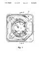
- FIGS. 1 and 2are a top plan view and a vertical cross sectional view respectively of a reactor suitable for carrying out the present process.
- the silicon oxide layers deposited in accordance with the inventionreduce or eliminate the surface sensitivity problem and the present process provides improved conformality and void-free gap filling capability to thermal CVD silicon oxide films, particularly when the silicon oxide is deposited over PECVD silicon oxide layers.
- the surface sensitivity of the deposited filmsis reduced by a very simple step, that of reducing the power during the final film deposition.
- the reduced power-deposited PECVD silicon oxideforms a different, interstitial film of silicon oxide. It is presently believed this film is a tensile film that modifies the surface of the PECVD silicon oxide layer, making it less hydrophilic.
- the second thermal CVD silicon oxide layerexhibits reduced surface sensitivity and improved film quality. This process is accomplished using the same prior known reaction conditions and gas precursor mixtures except for the power applied, which eliminates any need for a separate reaction chamber or changing reaction gases or conditions.
- the PECVD silicon oxide layer, the interstitial silicon oxide films and the thermal CVD silicon oxide layercan be deposited in the same reactor, using known gases, simply by controllably reducing the power at the end of the PECVD deposition, and then continuing with a thermal CVD deposition with the power off
- a PECVD processis carried out on the substrate.
- the PECVD oxide deposition processuses a plasma formed from TEOS, oxygen and a carrier gas, which can contain a helium diluent.
- This processuses a deposition chamber pressure of about 1-50 torr, preferably about 8.2 torr, an oxygen flow rate of about 100-1000 sccm, an inert carrier gas flow rate of about 100-1500 sccm, and RF power to a six inch diameter gas distributer cathode of about 200-400 watts. Power density at the gas distributor cathode is about 200-400 watts., or about 1 watt/cm 2 .
- the temperature of depositionis about 300°-500° C., preferably about 375° C. This process is described in greater detail in U.S. Pat. No. 4,872,947.
- the poweris controllably reduced in at least two steps; first to a level of below about 80% to about 55% of the initial power; and further reducing the power to a level of about 45-10% of power for an additional period.
- the poweris reduced in three stages; first to a level of about 80-65% of power for about 2 seconds; secondly to a level of about 50-35% of power for about 2 seconds; and lastly to a level of about 30-10% of power for a final 2 seconds.
- a maximum deposition period of about 8 secondsis employed for deposition of the reduced power interstitial silicon oxide layers. This gradual reduction of power produces silicon oxide layers having reduced surface sensitivity for overlying thermal CVD silicon oxide layers.
- FIGS. 1 and 2A suitable CVD/PECVD reactor in which the present process can be carried out is described in U.S. Pat. No. 4,872,947 to Chang et al assigned to Applied Materials, Inc, the assignee of the present invention.
- a top plan view an a vertical cross sectional view of a suitable reactorare shown in FIGS. 1 and 2.
- a reactor system 10comprises a vessel 12 that defines an inner vacuum chamber 13 that has a plasma processing region 14.
- the reactor system 10also includes a susceptor 16 for holding the substrate and a substrate transport system 18 that includes vertically movable substrate support fingers 20 and susceptor support fingers 22. These fingers cooperate with an external robotic blade 24 for introducing substrates 15 into the chamber 13 and depositing the substrates 15 on the susceptor 16 for processing and thereafter removing the substrates 15 from the susceptor 16 and the chamber 13.
- the reactor system 10further comprises a process/purge gas manifold 26 that applied process gas and purging gas to the chamber 13; a high frequency RF power supply and matching network 28, and a low frequency RF power supply and matching network 29 for creating and sustaining a process gas plasma from the inlet gas; and a lamp heating system 30 for heating the susceptor 16 and substrate 15 positioned on the susceptor 16 to effect deposition onto the substrate 15.
- High frequency RF power13.56 MHz
- lower RF frequencies100-450 KHz
- a mixture of high and low frequenciescan be used to generate a plasma from the process gases.
- a gas manifold 26supplies process gases to the chamber 13.
- the gas manifold 26distributes the process gases evenly radially outwardly across the substrate 15 to promote even deposition across the substrate 15, and can include a RF/gas feed-through device 36 that supplies process gas to the gas manifold 26 that is RF driven. This ensures a high degree of plasma confinement between the manifold 26 and the substrate 15, situate on the susceptor 16 which is grounded.
- a radiant heating systemcomprises an array of vertically oriented quartz-tungsten-halogen lamps 38 outside the chamber 13 which provide radiant heat to the susceptor 16 and the substrate 15 through a quartz window 40 in the chamber 13. Further details of the PECVD reactor are given in U.S. Pat. No. 4,872,947, incorporated herein by reference. Deposition of silicon oxide films can be deposited using standard high frequency RF power or a mixed frequency RF power can be used.
- the PECVD silicon oxide layeris generally deposited at a power level of the reactor of about 5 to 10 watts/cm 2 of the substrate, preferably about 7 watts/cm 2 .
- the powercan be stepwise reduced to about 5 watts/cm 2 , then reduced to about 3 watts/cm 2 and finally to about 1 watt/cm 2 , over a period of a few seconds. This process is reproducible and reliable.
- the same chambercan be used for both processes by simply deactivating the RF power for the thermal CVD silicon oxide deposition.
- thermal, conformal silicon oxidecan now be deposited that is of high quality and that does not exhibit the surface sensitivity of thermal CVD silicon oxide.
- the thermal CVD processuses a gas stream of TEOS, oxygen and ozone at fairly high pressures of over 10 torr, preferably from about 500 and 760 torr, and at substrate temperatures of about 375° C.
- a highly conformal silicon oxide layeris deposited that fills in stepped topographies on a silicon dioxide surface at a rapid deposition rate.
- the present processis highly advantageous because the first PECVD silicon oxide layer, the interstitial low power silicon oxide layers, and the final thermal CVD silicon oxide can be deposited in sequence, in the same reaction chamber, requiring a minimum of changes in the reactor, and without having to remove the substrate from the reaction chamber between deposition of the various layers.
- the chamber temperature and gas flow ratesremain constant during the PECVD depositions while the power levels of the RF source is reduced controllably and rapidly. It need take only about 6 seconds to deposit interstitial layers that reduce the surface sensitivity of the final thermal CVD silicon oxide layer.
Landscapes
- Engineering & Computer Science (AREA)
- Chemical & Material Sciences (AREA)
- Manufacturing & Machinery (AREA)
- General Physics & Mathematics (AREA)
- Physics & Mathematics (AREA)
- Computer Hardware Design (AREA)
- Microelectronics & Electronic Packaging (AREA)
- Power Engineering (AREA)
- Condensed Matter Physics & Semiconductors (AREA)
- Chemical Kinetics & Catalysis (AREA)
- Inorganic Chemistry (AREA)
- General Chemical & Material Sciences (AREA)
- Materials Engineering (AREA)
- Mechanical Engineering (AREA)
- Metallurgy (AREA)
- Organic Chemistry (AREA)
- Formation Of Insulating Films (AREA)
Abstract
Description
Claims (5)
Priority Applications (1)
| Application Number | Priority Date | Filing Date | Title |
|---|---|---|---|
| US07/930,121US5271972A (en) | 1992-08-17 | 1992-08-17 | Method for depositing ozone/TEOS silicon oxide films of reduced surface sensitivity |
Applications Claiming Priority (1)
| Application Number | Priority Date | Filing Date | Title |
|---|---|---|---|
| US07/930,121US5271972A (en) | 1992-08-17 | 1992-08-17 | Method for depositing ozone/TEOS silicon oxide films of reduced surface sensitivity |
Publications (1)
| Publication Number | Publication Date |
|---|---|
| US5271972Atrue US5271972A (en) | 1993-12-21 |
Family
ID=25458949
Family Applications (1)
| Application Number | Title | Priority Date | Filing Date |
|---|---|---|---|
| US07/930,121Expired - LifetimeUS5271972A (en) | 1992-08-17 | 1992-08-17 | Method for depositing ozone/TEOS silicon oxide films of reduced surface sensitivity |
Country Status (1)
| Country | Link |
|---|---|
| US (1) | US5271972A (en) |
Cited By (260)
| Publication number | Priority date | Publication date | Assignee | Title |
|---|---|---|---|---|
| US5399389A (en)* | 1992-08-04 | 1995-03-21 | Siemens Aktiengesellschaft | Method for locally and globally planarizing chemical vapor deposition of SiO2 layers onto structured silicon substrates |
| US5447884A (en)* | 1994-06-29 | 1995-09-05 | International Business Machines Corporation | Shallow trench isolation with thin nitride liner |
| US5554418A (en)* | 1993-12-28 | 1996-09-10 | Nihon Shinku Gijutsu Kabushiki Kaisha | Method of forming passivation film |
| US5563104A (en)* | 1995-06-23 | 1996-10-08 | Taiwan Semiconductor Manufacturing Company Ltd. | Reduction of pattern sensitivity in ozone-teos deposition via a two-step (low and high temperature) process |
| US5593741A (en)* | 1992-11-30 | 1997-01-14 | Nec Corporation | Method and apparatus for forming silicon oxide film by chemical vapor deposition |
| US5626924A (en)* | 1994-09-08 | 1997-05-06 | Sony Corporation | Method of forming oxide film |
| EP0778358A1 (en) | 1995-12-06 | 1997-06-11 | Applied Materials, Inc. | Method and apparatus for thin films formation by CVD |
| US5665644A (en)* | 1995-11-03 | 1997-09-09 | Micron Technology, Inc. | Semiconductor processing method of forming electrically conductive interconnect lines and integrated circuitry |
| US5795833A (en)* | 1996-08-01 | 1998-08-18 | Taiwan Semiconductor Manufacturing Company, Ltd | Method for fabricating passivation layers over metal lines |
| US5804509A (en)* | 1995-03-04 | 1998-09-08 | Hyundai Electronics Industries Co., Ltd. | Varying TEOS flow rate while forming intermetallic insulating layers in semiconductor devices |
| US5827569A (en)* | 1994-07-29 | 1998-10-27 | Akiyama; Shigeo | Hydrogen separation membrane and process for producing the same |
| US5840374A (en)* | 1993-12-28 | 1998-11-24 | Nihon Shinku Gijutsu Kabushiki Kaisha | Method of forming a SiO2 passivation film on a plastic substrate |
| US5926689A (en)* | 1995-12-19 | 1999-07-20 | International Business Machines Corporation | Process for reducing circuit damage during PECVD in single wafer PECVD system |
| US5981375A (en)* | 1996-07-11 | 1999-11-09 | Oki Electric Industry Co., Ltd. | Method of manufacturing a semiconductor device |
| US5997962A (en)* | 1995-06-30 | 1999-12-07 | Tokyo Electron Limited | Plasma process utilizing an electrostatic chuck |
| US6024044A (en)* | 1997-10-09 | 2000-02-15 | Applied Komatsu Technology, Inc. | Dual frequency excitation of plasma for film deposition |
| US6091150A (en)* | 1996-09-03 | 2000-07-18 | Micron Technology, Inc. | Integrated circuitry comprising electrically insulative material over interconnect line tops, sidewalls and bottoms |
| US6107214A (en)* | 1997-04-17 | 2000-08-22 | Micron Technology, Inc. | Method for improving thickness uniformity of deposited ozone-TEOS silicate glass layers |
| US6136685A (en)* | 1997-06-03 | 2000-10-24 | Applied Materials, Inc. | High deposition rate recipe for low dielectric constant films |
| US6139923A (en)* | 1996-02-09 | 2000-10-31 | Applied Materials, Inc. | Method and apparatus for reducing particle contamination in a substrate processing chamber |
| US6149987A (en)* | 1998-04-07 | 2000-11-21 | Applied Materials, Inc. | Method for depositing low dielectric constant oxide films |
| US6149974A (en)* | 1997-05-05 | 2000-11-21 | Applied Materials, Inc. | Method for elimination of TEOS/ozone silicon oxide surface sensitivity |
| EP1054444A1 (en)* | 1999-05-19 | 2000-11-22 | Applied Materials, Inc. | Process for depositing a porous, low dielectric constant silicon oxide film |
| US6197705B1 (en) | 1999-03-18 | 2001-03-06 | Chartered Semiconductor Manufacturing Ltd. | Method of silicon oxide and silicon glass films deposition |
| US6228232B1 (en) | 1998-07-09 | 2001-05-08 | Semitool, Inc. | Reactor vessel having improved cup anode and conductor assembly |
| US6335288B1 (en) | 2000-08-24 | 2002-01-01 | Applied Materials, Inc. | Gas chemistry cycling to achieve high aspect ratio gapfill with HDP-CVD |
| US6413583B1 (en) | 1998-02-11 | 2002-07-02 | Applied Materials, Inc. | Formation of a liquid-like silica layer by reaction of an organosilicon compound and a hydroxyl forming compound |
| US6482752B1 (en)* | 1993-10-26 | 2002-11-19 | Semiconductor Energy Laboratory Co., Ltd. | Substrate processing apparatus and method and a manufacturing method of a thin film semiconductor device |
| US6489254B1 (en)* | 2000-08-29 | 2002-12-03 | Atmel Corporation | Method of forming pre-metal dielectric film on a semiconductor substrate including first layer of undoped oxide of high ozone:TEOS volume ratio and second layer of low ozone doped BPSG |
| US20030003244A1 (en)* | 1998-03-20 | 2003-01-02 | Applied Materials, Inc. | Staggered in-situ deposition and etching of a dielectric layer for HDP CVD |
| US6521302B1 (en)* | 2000-09-26 | 2003-02-18 | Applied Materials, Inc. | Method of reducing plasma-induced damage |
| US6559061B2 (en) | 1998-07-31 | 2003-05-06 | Applied Materials, Inc. | Method and apparatus for forming improved metal interconnects |
| US20030124859A1 (en)* | 1998-09-29 | 2003-07-03 | Applied Materials, Inc. | CVD plasma assisted low dielectric constant films |
| US20030136332A1 (en)* | 2002-01-24 | 2003-07-24 | Applied Materials Inc., A Delaware Corporation | In situ application of etch back for improved deposition into high-aspect-ratio features |
| US20030140941A1 (en)* | 1986-09-09 | 2003-07-31 | Semiconductor Energy Laboratory Co., Ltd. | CVD apparatus |
| US20030207580A1 (en)* | 2002-05-03 | 2003-11-06 | Applied Materials, Inc. | HDP-CVD dep/etch/dep process for improved deposition into high aspect ratio features |
| US20030217916A1 (en)* | 2002-05-21 | 2003-11-27 | Woodruff Daniel J. | Electroplating reactor |
| US20040079728A1 (en)* | 2002-10-23 | 2004-04-29 | Applied Materials, Inc. | Reactive ion etching for semiconductor device feature topography modification |
| US20040079632A1 (en)* | 2002-10-23 | 2004-04-29 | Applied Materials, Inc. | High density plasma CVD process for gapfill into high aspect ratio features |
| US6753270B1 (en) | 2000-08-04 | 2004-06-22 | Applied Materials Inc. | Process for depositing a porous, low dielectric constant silicon oxide film |
| US20040241520A1 (en)* | 2003-05-31 | 2004-12-02 | Korea Institute Of Science And Technology | Method to manufacture composite polymer electrolyte membranes coated with inorganic thin films for fuel cells |
| US20040245091A1 (en)* | 2003-06-04 | 2004-12-09 | Applied Materials, Inc. | Hdp-cvd multistep gapfill process |
| US20040251236A1 (en)* | 2003-05-23 | 2004-12-16 | Applied Materials, Inc. | [deposition-selective etch-deposition process for dielectric film gapfill] |
| US20050023694A1 (en)* | 1998-02-11 | 2005-02-03 | Bjorkman Claes H. | Integrated low k dielectrics and etch stops |
| US6903031B2 (en) | 2003-09-03 | 2005-06-07 | Applied Materials, Inc. | In-situ-etch-assisted HDP deposition using SiF4 and hydrogen |
| US6911403B2 (en) | 2003-08-20 | 2005-06-28 | Applied Materials, Inc. | Methods of reducing plasma-induced damage for advanced plasma CVD dielectrics |
| US6916412B2 (en) | 1999-04-13 | 2005-07-12 | Semitool, Inc. | Adaptable electrochemical processing chamber |
| US6929700B2 (en) | 2001-05-11 | 2005-08-16 | Applied Materials, Inc. | Hydrogen assisted undoped silicon oxide deposition process for HDP-CVD |
| US6958112B2 (en) | 2003-05-27 | 2005-10-25 | Applied Materials, Inc. | Methods and systems for high-aspect-ratio gapfill using atomic-oxygen generation |
| US20060019031A1 (en)* | 2004-07-23 | 2006-01-26 | Applied Materials, Inc. | Deposition repeatability of PECVD films |
| US20060035035A1 (en)* | 1997-05-10 | 2006-02-16 | Semiconductor Energy Laboratory Co., Ltd. | Film forming method and film forming apparatus |
| US7020537B2 (en) | 1999-04-13 | 2006-03-28 | Semitool, Inc. | Tuning electrodes used in a reactor for electrochemically processing a microelectronic workpiece |
| US7030041B2 (en) | 2004-03-15 | 2006-04-18 | Applied Materials Inc. | Adhesion improvement for low k dielectrics |
| US20060154494A1 (en)* | 2005-01-08 | 2006-07-13 | Applied Materials, Inc., A Delaware Corporation | High-throughput HDP-CVD processes for advanced gapfill applications |
| US7087536B2 (en) | 2004-09-01 | 2006-08-08 | Applied Materials | Silicon oxide gapfill deposition using liquid precursors |
| US7115196B2 (en) | 1998-03-20 | 2006-10-03 | Semitool, Inc. | Apparatus and method for electrochemically depositing metal on a semiconductor workpiece |
| US20060252273A1 (en)* | 2005-05-04 | 2006-11-09 | Applied Materials, Inc. | Strengthening the interface between dielectric layers and barrier layers with an oxide layer of varying composition profile |
| US7147760B2 (en) | 1998-07-10 | 2006-12-12 | Semitool, Inc. | Electroplating apparatus with segmented anode array |
| US20060292894A1 (en)* | 2005-06-24 | 2006-12-28 | Applied Materials, Inc., | Gapfill using deposition-etch sequence |
| US7183227B1 (en) | 2004-07-01 | 2007-02-27 | Applied Materials, Inc. | Use of enhanced turbomolecular pump for gapfill deposition using high flows of low-mass fluent gas |
| US7189318B2 (en) | 1999-04-13 | 2007-03-13 | Semitool, Inc. | Tuning electrodes used in a reactor for electrochemically processing a microelectronic workpiece |
| US7196021B2 (en) | 2001-05-11 | 2007-03-27 | Applied Materials, Inc. | HDP-CVD deposition process for filling high aspect ratio gaps |
| US7229931B2 (en) | 2004-06-16 | 2007-06-12 | Applied Materials, Inc. | Oxygen plasma treatment for enhanced HDP-CVD gapfill |
| US20070155189A1 (en)* | 2006-01-04 | 2007-07-05 | Promos Technologies Pte. Ltd. | Use of TEOS oxides in integrated circuit fabrication processes |
| US7264698B2 (en) | 1999-04-13 | 2007-09-04 | Semitool, Inc. | Apparatus and methods for electrochemical processing of microelectronic workpieces |
| US7267749B2 (en) | 1999-04-13 | 2007-09-11 | Semitool, Inc. | Workpiece processor having processing chamber with improved processing fluid flow |
| US20070269958A1 (en)* | 2006-05-16 | 2007-11-22 | Li Li | Methods for filling trenches in a semiconductor material |
| US7351315B2 (en) | 2003-12-05 | 2008-04-01 | Semitool, Inc. | Chambers, systems, and methods for electrochemically processing microfeature workpieces |
| US7351314B2 (en) | 2003-12-05 | 2008-04-01 | Semitool, Inc. | Chambers, systems, and methods for electrochemically processing microfeature workpieces |
| US7438788B2 (en) | 1999-04-13 | 2008-10-21 | Semitool, Inc. | Apparatus and methods for electrochemical processing of microelectronic workpieces |
| US20080283933A1 (en)* | 2007-05-15 | 2008-11-20 | Shiu-Ko Jangjian | Oxygen-rich layers underlying BPSG |
| US20090014808A1 (en)* | 2007-07-15 | 2009-01-15 | Kyoung-Woo Lee | Methods For Forming Self-Aligned Dual Stress Liners For CMOS Semiconductor Devices |
| US7524750B2 (en) | 2006-04-17 | 2009-04-28 | Applied Materials, Inc. | Integrated process modulation (IPM) a novel solution for gapfill with HDP-CVD |
| US7585398B2 (en) | 1999-04-13 | 2009-09-08 | Semitool, Inc. | Chambers, systems, and methods for electrochemically processing microfeature workpieces |
| US7595088B2 (en) | 2003-01-23 | 2009-09-29 | Applied Materials, Inc. | Hydrogen assisted HDP-CVD deposition process for aggressive gap-fill technology |
| US20090291547A1 (en)* | 2008-05-22 | 2009-11-26 | Schraub David M | Method for Reducing Plasma Discharge Damage During Processing |
| US7678715B2 (en) | 2007-12-21 | 2010-03-16 | Applied Materials, Inc. | Low wet etch rate silicon nitride film |
| US20110014798A1 (en)* | 2007-10-22 | 2011-01-20 | Applied Materials, Inc. | High quality silicon oxide films by remote plasma cvd from disilane precursors |
| US7939422B2 (en) | 2006-12-07 | 2011-05-10 | Applied Materials, Inc. | Methods of thin film process |
| US20110223774A1 (en)* | 2010-03-09 | 2011-09-15 | Applied Materials, Inc. | REDUCED PATTERN LOADING USING BIS(DIETHYLAMINO)SILANE (C8H22N2Si) AS SILICON PRECURSOR |
| WO2011084812A3 (en)* | 2010-01-06 | 2011-11-17 | Applied Materials, Inc. | Flowable dielectric using oxide liner |
| US8232176B2 (en) | 2006-06-22 | 2012-07-31 | Applied Materials, Inc. | Dielectric deposition and etch back processes for bottom up gapfill |
| US8304351B2 (en) | 2010-01-07 | 2012-11-06 | Applied Materials, Inc. | In-situ ozone cure for radical-component CVD |
| US8318584B2 (en) | 2010-07-30 | 2012-11-27 | Applied Materials, Inc. | Oxide-rich liner layer for flowable CVD gapfill |
| US8329262B2 (en) | 2010-01-05 | 2012-12-11 | Applied Materials, Inc. | Dielectric film formation using inert gas excitation |
| US8357435B2 (en) | 2008-05-09 | 2013-01-22 | Applied Materials, Inc. | Flowable dielectric equipment and processes |
| US8445078B2 (en) | 2011-04-20 | 2013-05-21 | Applied Materials, Inc. | Low temperature silicon oxide conversion |
| US8449942B2 (en) | 2009-11-12 | 2013-05-28 | Applied Materials, Inc. | Methods of curing non-carbon flowable CVD films |
| US8450191B2 (en) | 2011-01-24 | 2013-05-28 | Applied Materials, Inc. | Polysilicon films by HDP-CVD |
| US8466073B2 (en) | 2011-06-03 | 2013-06-18 | Applied Materials, Inc. | Capping layer for reduced outgassing |
| US8497211B2 (en) | 2011-06-24 | 2013-07-30 | Applied Materials, Inc. | Integrated process modulation for PSG gapfill |
| US8524004B2 (en) | 2010-06-16 | 2013-09-03 | Applied Materials, Inc. | Loadlock batch ozone cure |
| US8551891B2 (en) | 2011-10-04 | 2013-10-08 | Applied Materials, Inc. | Remote plasma burn-in |
| US8563445B2 (en) | 2010-03-05 | 2013-10-22 | Applied Materials, Inc. | Conformal layers by radical-component CVD |
| US8617989B2 (en) | 2011-09-26 | 2013-12-31 | Applied Materials, Inc. | Liner property improvement |
| US8629067B2 (en) | 2009-12-30 | 2014-01-14 | Applied Materials, Inc. | Dielectric film growth with radicals produced using flexible nitrogen/hydrogen ratio |
| US8664127B2 (en) | 2010-10-15 | 2014-03-04 | Applied Materials, Inc. | Two silicon-containing precursors for gapfill enhancing dielectric liner |
| US8679983B2 (en) | 2011-09-01 | 2014-03-25 | Applied Materials, Inc. | Selective suppression of dry-etch rate of materials containing both silicon and nitrogen |
| US8679982B2 (en) | 2011-08-26 | 2014-03-25 | Applied Materials, Inc. | Selective suppression of dry-etch rate of materials containing both silicon and oxygen |
| US8716154B2 (en) | 2011-03-04 | 2014-05-06 | Applied Materials, Inc. | Reduced pattern loading using silicon oxide multi-layers |
| US8741778B2 (en) | 2010-12-14 | 2014-06-03 | Applied Materials, Inc. | Uniform dry etch in two stages |
| US8741788B2 (en) | 2009-08-06 | 2014-06-03 | Applied Materials, Inc. | Formation of silicon oxide using non-carbon flowable CVD processes |
| US8765574B2 (en) | 2012-11-09 | 2014-07-01 | Applied Materials, Inc. | Dry etch process |
| US8771536B2 (en) | 2011-08-01 | 2014-07-08 | Applied Materials, Inc. | Dry-etch for silicon-and-carbon-containing films |
| US8771539B2 (en) | 2011-02-22 | 2014-07-08 | Applied Materials, Inc. | Remotely-excited fluorine and water vapor etch |
| US8772178B2 (en)* | 2004-06-30 | 2014-07-08 | Globalfoundries Inc. | Technique for forming a dielectric interlayer above a structure including closely spaced lines |
| US8801952B1 (en) | 2013-03-07 | 2014-08-12 | Applied Materials, Inc. | Conformal oxide dry etch |
| US8808563B2 (en) | 2011-10-07 | 2014-08-19 | Applied Materials, Inc. | Selective etch of silicon by way of metastable hydrogen termination |
| US8895449B1 (en) | 2013-05-16 | 2014-11-25 | Applied Materials, Inc. | Delicate dry clean |
| US20140370698A1 (en)* | 2011-01-13 | 2014-12-18 | Spansion Llc | Non-Volatile Finfet Memory Array and Manufacturing Method Thereof |
| US8921234B2 (en) | 2012-12-21 | 2014-12-30 | Applied Materials, Inc. | Selective titanium nitride etching |
| US8927390B2 (en) | 2011-09-26 | 2015-01-06 | Applied Materials, Inc. | Intrench profile |
| US8951429B1 (en) | 2013-10-29 | 2015-02-10 | Applied Materials, Inc. | Tungsten oxide processing |
| US8956980B1 (en) | 2013-09-16 | 2015-02-17 | Applied Materials, Inc. | Selective etch of silicon nitride |
| US8969212B2 (en) | 2012-11-20 | 2015-03-03 | Applied Materials, Inc. | Dry-etch selectivity |
| US8975152B2 (en) | 2011-11-08 | 2015-03-10 | Applied Materials, Inc. | Methods of reducing substrate dislocation during gapfill processing |
| US8980763B2 (en) | 2012-11-30 | 2015-03-17 | Applied Materials, Inc. | Dry-etch for selective tungsten removal |
| US8980382B2 (en) | 2009-12-02 | 2015-03-17 | Applied Materials, Inc. | Oxygen-doping for non-carbon radical-component CVD films |
| US8999856B2 (en) | 2011-03-14 | 2015-04-07 | Applied Materials, Inc. | Methods for etch of sin films |
| US9018108B2 (en) | 2013-01-25 | 2015-04-28 | Applied Materials, Inc. | Low shrinkage dielectric films |
| US9023734B2 (en) | 2012-09-18 | 2015-05-05 | Applied Materials, Inc. | Radical-component oxide etch |
| US9023732B2 (en) | 2013-03-15 | 2015-05-05 | Applied Materials, Inc. | Processing systems and methods for halide scavenging |
| US9034770B2 (en) | 2012-09-17 | 2015-05-19 | Applied Materials, Inc. | Differential silicon oxide etch |
| US9040422B2 (en) | 2013-03-05 | 2015-05-26 | Applied Materials, Inc. | Selective titanium nitride removal |
| US9064815B2 (en) | 2011-03-14 | 2015-06-23 | Applied Materials, Inc. | Methods for etch of metal and metal-oxide films |
| US9064816B2 (en) | 2012-11-30 | 2015-06-23 | Applied Materials, Inc. | Dry-etch for selective oxidation removal |
| US9111877B2 (en) | 2012-12-18 | 2015-08-18 | Applied Materials, Inc. | Non-local plasma oxide etch |
| US20150235850A1 (en)* | 2014-02-20 | 2015-08-20 | Tokyo Electron Limited | Semiconductor device manufacturing method and semiconductor device manufacturing apparatus |
| US9117855B2 (en) | 2013-12-04 | 2015-08-25 | Applied Materials, Inc. | Polarity control for remote plasma |
| US9114438B2 (en) | 2013-05-21 | 2015-08-25 | Applied Materials, Inc. | Copper residue chamber clean |
| US9136273B1 (en) | 2014-03-21 | 2015-09-15 | Applied Materials, Inc. | Flash gate air gap |
| US9132436B2 (en) | 2012-09-21 | 2015-09-15 | Applied Materials, Inc. | Chemical control features in wafer process equipment |
| US9159606B1 (en) | 2014-07-31 | 2015-10-13 | Applied Materials, Inc. | Metal air gap |
| US9165786B1 (en) | 2014-08-05 | 2015-10-20 | Applied Materials, Inc. | Integrated oxide and nitride recess for better channel contact in 3D architectures |
| US9190293B2 (en) | 2013-12-18 | 2015-11-17 | Applied Materials, Inc. | Even tungsten etch for high aspect ratio trenches |
| US9236265B2 (en) | 2013-11-04 | 2016-01-12 | Applied Materials, Inc. | Silicon germanium processing |
| US9245762B2 (en) | 2013-12-02 | 2016-01-26 | Applied Materials, Inc. | Procedure for etch rate consistency |
| US9263278B2 (en) | 2013-12-17 | 2016-02-16 | Applied Materials, Inc. | Dopant etch selectivity control |
| US9269590B2 (en) | 2014-04-07 | 2016-02-23 | Applied Materials, Inc. | Spacer formation |
| US9285168B2 (en) | 2010-10-05 | 2016-03-15 | Applied Materials, Inc. | Module for ozone cure and post-cure moisture treatment |
| US9287095B2 (en) | 2013-12-17 | 2016-03-15 | Applied Materials, Inc. | Semiconductor system assemblies and methods of operation |
| US9287134B2 (en) | 2014-01-17 | 2016-03-15 | Applied Materials, Inc. | Titanium oxide etch |
| US9293568B2 (en) | 2014-01-27 | 2016-03-22 | Applied Materials, Inc. | Method of fin patterning |
| US9299538B2 (en) | 2014-03-20 | 2016-03-29 | Applied Materials, Inc. | Radial waveguide systems and methods for post-match control of microwaves |
| US9299582B2 (en) | 2013-11-12 | 2016-03-29 | Applied Materials, Inc. | Selective etch for metal-containing materials |
| US9299575B2 (en) | 2014-03-17 | 2016-03-29 | Applied Materials, Inc. | Gas-phase tungsten etch |
| US9299537B2 (en) | 2014-03-20 | 2016-03-29 | Applied Materials, Inc. | Radial waveguide systems and methods for post-match control of microwaves |
| US9299583B1 (en) | 2014-12-05 | 2016-03-29 | Applied Materials, Inc. | Aluminum oxide selective etch |
| US9309598B2 (en) | 2014-05-28 | 2016-04-12 | Applied Materials, Inc. | Oxide and metal removal |
| US9324576B2 (en) | 2010-05-27 | 2016-04-26 | Applied Materials, Inc. | Selective etch for silicon films |
| US9343272B1 (en) | 2015-01-08 | 2016-05-17 | Applied Materials, Inc. | Self-aligned process |
| US9349605B1 (en) | 2015-08-07 | 2016-05-24 | Applied Materials, Inc. | Oxide etch selectivity systems and methods |
| US9355856B2 (en) | 2014-09-12 | 2016-05-31 | Applied Materials, Inc. | V trench dry etch |
| US9355862B2 (en) | 2014-09-24 | 2016-05-31 | Applied Materials, Inc. | Fluorine-based hardmask removal |
| US9362130B2 (en) | 2013-03-01 | 2016-06-07 | Applied Materials, Inc. | Enhanced etching processes using remote plasma sources |
| US9368364B2 (en) | 2014-09-24 | 2016-06-14 | Applied Materials, Inc. | Silicon etch process with tunable selectivity to SiO2 and other materials |
| US9373522B1 (en) | 2015-01-22 | 2016-06-21 | Applied Mateials, Inc. | Titanium nitride removal |
| US9373517B2 (en) | 2012-08-02 | 2016-06-21 | Applied Materials, Inc. | Semiconductor processing with DC assisted RF power for improved control |
| US9378978B2 (en) | 2014-07-31 | 2016-06-28 | Applied Materials, Inc. | Integrated oxide recess and floating gate fin trimming |
| US9378969B2 (en) | 2014-06-19 | 2016-06-28 | Applied Materials, Inc. | Low temperature gas-phase carbon removal |
| US9385028B2 (en) | 2014-02-03 | 2016-07-05 | Applied Materials, Inc. | Air gap process |
| US9390937B2 (en) | 2012-09-20 | 2016-07-12 | Applied Materials, Inc. | Silicon-carbon-nitride selective etch |
| US9396989B2 (en) | 2014-01-27 | 2016-07-19 | Applied Materials, Inc. | Air gaps between copper lines |
| US9404178B2 (en) | 2011-07-15 | 2016-08-02 | Applied Materials, Inc. | Surface treatment and deposition for reduced outgassing |
| US9406523B2 (en) | 2014-06-19 | 2016-08-02 | Applied Materials, Inc. | Highly selective doped oxide removal method |
| US9425058B2 (en) | 2014-07-24 | 2016-08-23 | Applied Materials, Inc. | Simplified litho-etch-litho-etch process |
| US9449846B2 (en) | 2015-01-28 | 2016-09-20 | Applied Materials, Inc. | Vertical gate separation |
| US9478432B2 (en) | 2014-09-25 | 2016-10-25 | Applied Materials, Inc. | Silicon oxide selective removal |
| US9493879B2 (en) | 2013-07-12 | 2016-11-15 | Applied Materials, Inc. | Selective sputtering for pattern transfer |
| US9496167B2 (en) | 2014-07-31 | 2016-11-15 | Applied Materials, Inc. | Integrated bit-line airgap formation and gate stack post clean |
| US9502258B2 (en) | 2014-12-23 | 2016-11-22 | Applied Materials, Inc. | Anisotropic gap etch |
| US9499898B2 (en) | 2014-03-03 | 2016-11-22 | Applied Materials, Inc. | Layered thin film heater and method of fabrication |
| US9553102B2 (en) | 2014-08-19 | 2017-01-24 | Applied Materials, Inc. | Tungsten separation |
| US9576809B2 (en) | 2013-11-04 | 2017-02-21 | Applied Materials, Inc. | Etch suppression with germanium |
| US9659753B2 (en) | 2014-08-07 | 2017-05-23 | Applied Materials, Inc. | Grooved insulator to reduce leakage current |
| US9691645B2 (en) | 2015-08-06 | 2017-06-27 | Applied Materials, Inc. | Bolted wafer chuck thermal management systems and methods for wafer processing systems |
| US9721789B1 (en) | 2016-10-04 | 2017-08-01 | Applied Materials, Inc. | Saving ion-damaged spacers |
| US9728437B2 (en) | 2015-02-03 | 2017-08-08 | Applied Materials, Inc. | High temperature chuck for plasma processing systems |
| US9728450B2 (en) | 2015-06-25 | 2017-08-08 | International Business Machines Corporation | Insulating a via in a semiconductor substrate |
| US9741593B2 (en) | 2015-08-06 | 2017-08-22 | Applied Materials, Inc. | Thermal management systems and methods for wafer processing systems |
| US9768034B1 (en) | 2016-11-11 | 2017-09-19 | Applied Materials, Inc. | Removal methods for high aspect ratio structures |
| US9773648B2 (en) | 2013-08-30 | 2017-09-26 | Applied Materials, Inc. | Dual discharge modes operation for remote plasma |
| US9847289B2 (en) | 2014-05-30 | 2017-12-19 | Applied Materials, Inc. | Protective via cap for improved interconnect performance |
| US9865484B1 (en) | 2016-06-29 | 2018-01-09 | Applied Materials, Inc. | Selective etch using material modification and RF pulsing |
| US9881805B2 (en) | 2015-03-02 | 2018-01-30 | Applied Materials, Inc. | Silicon selective removal |
| US9885117B2 (en) | 2014-03-31 | 2018-02-06 | Applied Materials, Inc. | Conditioned semiconductor system parts |
| US9934942B1 (en) | 2016-10-04 | 2018-04-03 | Applied Materials, Inc. | Chamber with flow-through source |
| US9947549B1 (en) | 2016-10-10 | 2018-04-17 | Applied Materials, Inc. | Cobalt-containing material removal |
| US10026621B2 (en) | 2016-11-14 | 2018-07-17 | Applied Materials, Inc. | SiN spacer profile patterning |
| US10043674B1 (en) | 2017-08-04 | 2018-08-07 | Applied Materials, Inc. | Germanium etching systems and methods |
| US10043684B1 (en) | 2017-02-06 | 2018-08-07 | Applied Materials, Inc. | Self-limiting atomic thermal etching systems and methods |
| US10049891B1 (en) | 2017-05-31 | 2018-08-14 | Applied Materials, Inc. | Selective in situ cobalt residue removal |
| US10062579B2 (en) | 2016-10-07 | 2018-08-28 | Applied Materials, Inc. | Selective SiN lateral recess |
| US10062587B2 (en) | 2012-07-18 | 2018-08-28 | Applied Materials, Inc. | Pedestal with multi-zone temperature control and multiple purge capabilities |
| US10062585B2 (en) | 2016-10-04 | 2018-08-28 | Applied Materials, Inc. | Oxygen compatible plasma source |
| US10062575B2 (en) | 2016-09-09 | 2018-08-28 | Applied Materials, Inc. | Poly directional etch by oxidation |
| US10128086B1 (en) | 2017-10-24 | 2018-11-13 | Applied Materials, Inc. | Silicon pretreatment for nitride removal |
| US10163696B2 (en) | 2016-11-11 | 2018-12-25 | Applied Materials, Inc. | Selective cobalt removal for bottom up gapfill |
| US10170282B2 (en) | 2013-03-08 | 2019-01-01 | Applied Materials, Inc. | Insulated semiconductor faceplate designs |
| US10170336B1 (en) | 2017-08-04 | 2019-01-01 | Applied Materials, Inc. | Methods for anisotropic control of selective silicon removal |
| US10224210B2 (en) | 2014-12-09 | 2019-03-05 | Applied Materials, Inc. | Plasma processing system with direct outlet toroidal plasma source |
| US10242908B2 (en) | 2016-11-14 | 2019-03-26 | Applied Materials, Inc. | Airgap formation with damage-free copper |
| US10256112B1 (en) | 2017-12-08 | 2019-04-09 | Applied Materials, Inc. | Selective tungsten removal |
| US10256079B2 (en) | 2013-02-08 | 2019-04-09 | Applied Materials, Inc. | Semiconductor processing systems having multiple plasma configurations |
| US10283324B1 (en) | 2017-10-24 | 2019-05-07 | Applied Materials, Inc. | Oxygen treatment for nitride etching |
| US10283321B2 (en) | 2011-01-18 | 2019-05-07 | Applied Materials, Inc. | Semiconductor processing system and methods using capacitively coupled plasma |
| US10297458B2 (en) | 2017-08-07 | 2019-05-21 | Applied Materials, Inc. | Process window widening using coated parts in plasma etch processes |
| US10319600B1 (en) | 2018-03-12 | 2019-06-11 | Applied Materials, Inc. | Thermal silicon etch |
| US10319649B2 (en) | 2017-04-11 | 2019-06-11 | Applied Materials, Inc. | Optical emission spectroscopy (OES) for remote plasma monitoring |
| US10319739B2 (en) | 2017-02-08 | 2019-06-11 | Applied Materials, Inc. | Accommodating imperfectly aligned memory holes |
| US10354889B2 (en) | 2017-07-17 | 2019-07-16 | Applied Materials, Inc. | Non-halogen etching of silicon-containing materials |
| US10403507B2 (en) | 2017-02-03 | 2019-09-03 | Applied Materials, Inc. | Shaped etch profile with oxidation |
| US20190287843A1 (en)* | 2018-03-14 | 2019-09-19 | Kokusai Electric Corporation | Substrate processing apparatus and method of manufacturing semiconductor device |
| US10431429B2 (en) | 2017-02-03 | 2019-10-01 | Applied Materials, Inc. | Systems and methods for radial and azimuthal control of plasma uniformity |
| US10468267B2 (en) | 2017-05-31 | 2019-11-05 | Applied Materials, Inc. | Water-free etching methods |
| US10483282B2 (en)* | 2015-08-27 | 2019-11-19 | Applied Materials, Inc. | VNAND tensile thick TEOS oxide |
| US10490406B2 (en) | 2018-04-10 | 2019-11-26 | Appled Materials, Inc. | Systems and methods for material breakthrough |
| US10490418B2 (en) | 2014-10-14 | 2019-11-26 | Applied Materials, Inc. | Systems and methods for internal surface conditioning assessment in plasma processing equipment |
| US10497573B2 (en) | 2018-03-13 | 2019-12-03 | Applied Materials, Inc. | Selective atomic layer etching of semiconductor materials |
| US10504754B2 (en) | 2016-05-19 | 2019-12-10 | Applied Materials, Inc. | Systems and methods for improved semiconductor etching and component protection |
| US10504700B2 (en) | 2015-08-27 | 2019-12-10 | Applied Materials, Inc. | Plasma etching systems and methods with secondary plasma injection |
| US10522371B2 (en) | 2016-05-19 | 2019-12-31 | Applied Materials, Inc. | Systems and methods for improved semiconductor etching and component protection |
| US10541246B2 (en) | 2017-06-26 | 2020-01-21 | Applied Materials, Inc. | 3D flash memory cells which discourage cross-cell electrical tunneling |
| US10541184B2 (en) | 2017-07-11 | 2020-01-21 | Applied Materials, Inc. | Optical emission spectroscopic techniques for monitoring etching |
| US10546729B2 (en) | 2016-10-04 | 2020-01-28 | Applied Materials, Inc. | Dual-channel showerhead with improved profile |
| US10566206B2 (en) | 2016-12-27 | 2020-02-18 | Applied Materials, Inc. | Systems and methods for anisotropic material breakthrough |
| US10573496B2 (en) | 2014-12-09 | 2020-02-25 | Applied Materials, Inc. | Direct outlet toroidal plasma source |
| US10573527B2 (en) | 2018-04-06 | 2020-02-25 | Applied Materials, Inc. | Gas-phase selective etching systems and methods |
| US10593523B2 (en) | 2014-10-14 | 2020-03-17 | Applied Materials, Inc. | Systems and methods for internal surface conditioning in plasma processing equipment |
| US10593560B2 (en) | 2018-03-01 | 2020-03-17 | Applied Materials, Inc. | Magnetic induction plasma source for semiconductor processes and equipment |
| US10615047B2 (en) | 2018-02-28 | 2020-04-07 | Applied Materials, Inc. | Systems and methods to form airgaps |
| US10629473B2 (en) | 2016-09-09 | 2020-04-21 | Applied Materials, Inc. | Footing removal for nitride spacer |
| US10672642B2 (en) | 2018-07-24 | 2020-06-02 | Applied Materials, Inc. | Systems and methods for pedestal configuration |
| US10679870B2 (en) | 2018-02-15 | 2020-06-09 | Applied Materials, Inc. | Semiconductor processing chamber multistage mixing apparatus |
| US10699879B2 (en) | 2018-04-17 | 2020-06-30 | Applied Materials, Inc. | Two piece electrode assembly with gap for plasma control |
| US10727080B2 (en) | 2017-07-07 | 2020-07-28 | Applied Materials, Inc. | Tantalum-containing material removal |
| US10755941B2 (en) | 2018-07-06 | 2020-08-25 | Applied Materials, Inc. | Self-limiting selective etching systems and methods |
| US10854426B2 (en) | 2018-01-08 | 2020-12-01 | Applied Materials, Inc. | Metal recess for semiconductor structures |
| US10872778B2 (en) | 2018-07-06 | 2020-12-22 | Applied Materials, Inc. | Systems and methods utilizing solid-phase etchants |
| US10886137B2 (en) | 2018-04-30 | 2021-01-05 | Applied Materials, Inc. | Selective nitride removal |
| US10892198B2 (en) | 2018-09-14 | 2021-01-12 | Applied Materials, Inc. | Systems and methods for improved performance in semiconductor processing |
| US10903054B2 (en) | 2017-12-19 | 2021-01-26 | Applied Materials, Inc. | Multi-zone gas distribution systems and methods |
| US10920319B2 (en) | 2019-01-11 | 2021-02-16 | Applied Materials, Inc. | Ceramic showerheads with conductive electrodes |
| US10920320B2 (en) | 2017-06-16 | 2021-02-16 | Applied Materials, Inc. | Plasma health determination in semiconductor substrate processing reactors |
| US10943834B2 (en) | 2017-03-13 | 2021-03-09 | Applied Materials, Inc. | Replacement contact process |
| US10964512B2 (en) | 2018-02-15 | 2021-03-30 | Applied Materials, Inc. | Semiconductor processing chamber multistage mixing apparatus and methods |
| US11049755B2 (en) | 2018-09-14 | 2021-06-29 | Applied Materials, Inc. | Semiconductor substrate supports with embedded RF shield |
| US11062887B2 (en) | 2018-09-17 | 2021-07-13 | Applied Materials, Inc. | High temperature RF heater pedestals |
| US11121002B2 (en) | 2018-10-24 | 2021-09-14 | Applied Materials, Inc. | Systems and methods for etching metals and metal derivatives |
| US11239061B2 (en) | 2014-11-26 | 2022-02-01 | Applied Materials, Inc. | Methods and systems to enhance process uniformity |
| US11257693B2 (en) | 2015-01-09 | 2022-02-22 | Applied Materials, Inc. | Methods and systems to improve pedestal temperature control |
| US11276590B2 (en) | 2017-05-17 | 2022-03-15 | Applied Materials, Inc. | Multi-zone semiconductor substrate supports |
| US11276559B2 (en) | 2017-05-17 | 2022-03-15 | Applied Materials, Inc. | Semiconductor processing chamber for multiple precursor flow |
| US11328909B2 (en) | 2017-12-22 | 2022-05-10 | Applied Materials, Inc. | Chamber conditioning and removal processes |
| US11417534B2 (en) | 2018-09-21 | 2022-08-16 | Applied Materials, Inc. | Selective material removal |
| US11437242B2 (en) | 2018-11-27 | 2022-09-06 | Applied Materials, Inc. | Selective removal of silicon-containing materials |
| US11594428B2 (en) | 2015-02-03 | 2023-02-28 | Applied Materials, Inc. | Low temperature chuck for plasma processing systems |
| US11682560B2 (en) | 2018-10-11 | 2023-06-20 | Applied Materials, Inc. | Systems and methods for hafnium-containing film removal |
| US11721527B2 (en) | 2019-01-07 | 2023-08-08 | Applied Materials, Inc. | Processing chamber mixing systems |
| US12340979B2 (en) | 2017-05-17 | 2025-06-24 | Applied Materials, Inc. | Semiconductor processing chamber for improved precursor flow |
Citations (2)
| Publication number | Priority date | Publication date | Assignee | Title |
|---|---|---|---|---|
| US4872947A (en)* | 1986-12-19 | 1989-10-10 | Applied Materials, Inc. | CVD of silicon oxide using TEOS decomposition and in-situ planarization process |
| US4987005A (en)* | 1986-08-08 | 1991-01-22 | Semiconductor Energy Laboratory Co., Ltd. | Chemical vapor processing method for deposition or etching on a plurality of substrates |
- 1992
- 1992-08-17USUS07/930,121patent/US5271972A/ennot_activeExpired - Lifetime
Patent Citations (2)
| Publication number | Priority date | Publication date | Assignee | Title |
|---|---|---|---|---|
| US4987005A (en)* | 1986-08-08 | 1991-01-22 | Semiconductor Energy Laboratory Co., Ltd. | Chemical vapor processing method for deposition or etching on a plurality of substrates |
| US4872947A (en)* | 1986-12-19 | 1989-10-10 | Applied Materials, Inc. | CVD of silicon oxide using TEOS decomposition and in-situ planarization process |
Non-Patent Citations (2)
| Title |
|---|
| Fujino et al., J. Electrochem. Soc. vol. 138, No. 2 Feb. 1991 pp. 550 553.* |
| Fujino et al., J. Electrochem. Soc. vol. 138, No. 2 Feb. 1991 pp. 550-553. |
Cited By (428)
| Publication number | Priority date | Publication date | Assignee | Title |
|---|---|---|---|---|
| US20030140941A1 (en)* | 1986-09-09 | 2003-07-31 | Semiconductor Energy Laboratory Co., Ltd. | CVD apparatus |
| US5399389A (en)* | 1992-08-04 | 1995-03-21 | Siemens Aktiengesellschaft | Method for locally and globally planarizing chemical vapor deposition of SiO2 layers onto structured silicon substrates |
| US5593741A (en)* | 1992-11-30 | 1997-01-14 | Nec Corporation | Method and apparatus for forming silicon oxide film by chemical vapor deposition |
| US20020197760A1 (en)* | 1993-10-26 | 2002-12-26 | Semiconductor Energy Laboratory Co., Ltd. | Substrate processing apparatus and method and a manufacturing method of a thin film semiconductor device |
| US8304350B2 (en) | 1993-10-26 | 2012-11-06 | Semiconductor Energy Laboratory Co., Ltd. | Method of manufacturing a semiconductor device |
| US20100144077A1 (en)* | 1993-10-26 | 2010-06-10 | Semiconductor Energy Laboratory Co., Ltd. | Substrate processing apparatus and method and a manufacturing method of a thin film semiconductor device |
| US7271082B2 (en) | 1993-10-26 | 2007-09-18 | Semiconductor Energy Laboratory Co., Ltd. | Method of manufacturing a semiconductor device |
| US7691692B2 (en) | 1993-10-26 | 2010-04-06 | Semiconductor Energy Laboratory Co., Ltd. | Substrate processing apparatus and a manufacturing method of a thin film semiconductor device |
| US6482752B1 (en)* | 1993-10-26 | 2002-11-19 | Semiconductor Energy Laboratory Co., Ltd. | Substrate processing apparatus and method and a manufacturing method of a thin film semiconductor device |
| US20090029509A1 (en)* | 1993-10-26 | 2009-01-29 | Semiconductor Energy Laboratory Co., Ltd. | Substrate processing apparatus and method and a manufacturing method of a thin film semiconductor device |
| US20070173046A1 (en)* | 1993-10-26 | 2007-07-26 | Semiconductor Energy Laboratory Co., Ltd. | Substrate processing apparatus and method and a manufacturing method of a thin film semiconductor device |
| US7452794B2 (en) | 1993-10-26 | 2008-11-18 | Semiconductor Energy Laboratory Co., Ltd. | Manufacturing method of a thin film semiconductor device |
| US5554418A (en)* | 1993-12-28 | 1996-09-10 | Nihon Shinku Gijutsu Kabushiki Kaisha | Method of forming passivation film |
| US5840374A (en)* | 1993-12-28 | 1998-11-24 | Nihon Shinku Gijutsu Kabushiki Kaisha | Method of forming a SiO2 passivation film on a plastic substrate |
| US5447884A (en)* | 1994-06-29 | 1995-09-05 | International Business Machines Corporation | Shallow trench isolation with thin nitride liner |
| US5827569A (en)* | 1994-07-29 | 1998-10-27 | Akiyama; Shigeo | Hydrogen separation membrane and process for producing the same |
| US5626924A (en)* | 1994-09-08 | 1997-05-06 | Sony Corporation | Method of forming oxide film |
| US5804509A (en)* | 1995-03-04 | 1998-09-08 | Hyundai Electronics Industries Co., Ltd. | Varying TEOS flow rate while forming intermetallic insulating layers in semiconductor devices |
| US5563104A (en)* | 1995-06-23 | 1996-10-08 | Taiwan Semiconductor Manufacturing Company Ltd. | Reduction of pattern sensitivity in ozone-teos deposition via a two-step (low and high temperature) process |
| US5997962A (en)* | 1995-06-30 | 1999-12-07 | Tokyo Electron Limited | Plasma process utilizing an electrostatic chuck |
| US6066553A (en)* | 1995-11-03 | 2000-05-23 | Micron Technology, Inc. | Semiconductor processing method of forming electrically conductive interconnect lines and integrated circuitry |
| US6432813B1 (en) | 1995-11-03 | 2002-08-13 | Micron Technology, Inc. | Semiconductor processing method of forming insulative material over conductive lines |
| US5665644A (en)* | 1995-11-03 | 1997-09-09 | Micron Technology, Inc. | Semiconductor processing method of forming electrically conductive interconnect lines and integrated circuitry |
| US6009827A (en)* | 1995-12-06 | 2000-01-04 | Applied Materials, Inc. | Apparatus for creating strong interface between in-situ SACVD and PECVD silicon oxide films |
| EP0778358A1 (en) | 1995-12-06 | 1997-06-11 | Applied Materials, Inc. | Method and apparatus for thin films formation by CVD |
| US5814377A (en)* | 1995-12-06 | 1998-09-29 | Applied Materials, Inc. | Method and apparatus for creating strong interface between in-situ SACVD and PECVD silicon oxide films |
| US5926689A (en)* | 1995-12-19 | 1999-07-20 | International Business Machines Corporation | Process for reducing circuit damage during PECVD in single wafer PECVD system |
| US6139923A (en)* | 1996-02-09 | 2000-10-31 | Applied Materials, Inc. | Method and apparatus for reducing particle contamination in a substrate processing chamber |
| US6465043B1 (en)* | 1996-02-09 | 2002-10-15 | Applied Materials, Inc. | Method and apparatus for reducing particle contamination in a substrate processing chamber |
| US5981375A (en)* | 1996-07-11 | 1999-11-09 | Oki Electric Industry Co., Ltd. | Method of manufacturing a semiconductor device |
| US5795833A (en)* | 1996-08-01 | 1998-08-18 | Taiwan Semiconductor Manufacturing Company, Ltd | Method for fabricating passivation layers over metal lines |
| US6091150A (en)* | 1996-09-03 | 2000-07-18 | Micron Technology, Inc. | Integrated circuitry comprising electrically insulative material over interconnect line tops, sidewalls and bottoms |
| US20050255689A1 (en)* | 1997-04-17 | 2005-11-17 | Ravi Iyer | Method for improving thickness uniformity of deposited ozone-TEOS silicate glass layers |
| US6251807B1 (en) | 1997-04-17 | 2001-06-26 | Micron Technology, Inc. | Method for improving thickness uniformity of deposited ozone-teos silicate glass layers |
| US6815374B2 (en) | 1997-04-17 | 2004-11-09 | Micron Technology, Inc. | Method for improving thickness uniformity of deposited ozone-TEOS silicate glass layers |
| US6784122B2 (en) | 1997-04-17 | 2004-08-31 | Micron Technology, Inc. | Method for improving thickness uniformity of deposited ozone-TEOS silicate glass layers |
| US20050032394A1 (en)* | 1997-04-17 | 2005-02-10 | Ravi Iyer | Method for improving thickness uniformity of deposited ozone-TEOS silicate glass layers |
| US6297175B1 (en) | 1997-04-17 | 2001-10-02 | Micron Technology Inc. | Method for improving thickness uniformity of deposited ozone-TEOS silicate glass layers |
| US20030203654A1 (en)* | 1997-04-17 | 2003-10-30 | Ravi Iyer | Method for improving thickness uniformity of deposited ozone-teos silicate glass layers |
| US6576570B2 (en) | 1997-04-17 | 2003-06-10 | Micron Technology, Inc. | Method for improving thickness uniformity of deposited ozone-teos silicate glass layers |
| US6458721B2 (en) | 1997-04-17 | 2002-10-01 | Micron Technology, Inc. | Method for improving thickness uniformity of deposited ozone-TEOS silicate glass layers |
| US6107214A (en)* | 1997-04-17 | 2000-08-22 | Micron Technology, Inc. | Method for improving thickness uniformity of deposited ozone-TEOS silicate glass layers |
| US7101815B2 (en) | 1997-04-17 | 2006-09-05 | Micron Technology, Inc. | Method for improving thickness uniformity of deposited ozone-TEOS silicate glass layers |
| US6149974A (en)* | 1997-05-05 | 2000-11-21 | Applied Materials, Inc. | Method for elimination of TEOS/ozone silicon oxide surface sensitivity |
| US6319324B1 (en) | 1997-05-05 | 2001-11-20 | Applied Materials, Inc. | Method and apparatus for elimination of TEOS/ozone silicon oxide surface sensitivity |
| US20060035035A1 (en)* | 1997-05-10 | 2006-02-16 | Semiconductor Energy Laboratory Co., Ltd. | Film forming method and film forming apparatus |
| US6136685A (en)* | 1997-06-03 | 2000-10-24 | Applied Materials, Inc. | High deposition rate recipe for low dielectric constant films |
| US6024044A (en)* | 1997-10-09 | 2000-02-15 | Applied Komatsu Technology, Inc. | Dual frequency excitation of plasma for film deposition |
| US7227244B2 (en) | 1998-02-11 | 2007-06-05 | Applied Materials, Inc. | Integrated low k dielectrics and etch stops |
| US6858153B2 (en) | 1998-02-11 | 2005-02-22 | Applied Materials Inc. | Integrated low K dielectrics and etch stops |
| US6413583B1 (en) | 1998-02-11 | 2002-07-02 | Applied Materials, Inc. | Formation of a liquid-like silica layer by reaction of an organosilicon compound and a hydroxyl forming compound |
| US20050023694A1 (en)* | 1998-02-11 | 2005-02-03 | Bjorkman Claes H. | Integrated low k dielectrics and etch stops |
| US7115196B2 (en) | 1998-03-20 | 2006-10-03 | Semitool, Inc. | Apparatus and method for electrochemically depositing metal on a semiconductor workpiece |
| US7132134B2 (en) | 1998-03-20 | 2006-11-07 | Applied Materials, Inc. | Staggered in-situ deposition and etching of a dielectric layer for HDP CVD |
| US20030003244A1 (en)* | 1998-03-20 | 2003-01-02 | Applied Materials, Inc. | Staggered in-situ deposition and etching of a dielectric layer for HDP CVD |
| US20070071908A1 (en)* | 1998-03-20 | 2007-03-29 | Applied Materials, Inc. | Staggered in-situ deposition and etching of a dielectric layer for HDP-CVD |
| US7455893B2 (en) | 1998-03-20 | 2008-11-25 | Applied Materials, Inc. | Staggered in-situ deposition and etching of a dielectric layer for HDP-CVD |
| US20050032382A1 (en)* | 1998-03-20 | 2005-02-10 | Applied Materials, Inc. | Staggered in-situ deposition and etching of a dielectric layer for HDP CVD |
| US6821577B2 (en) | 1998-03-20 | 2004-11-23 | Applied Materials, Inc. | Staggered in-situ deposition and etching of a dielectric layer for HDP CVD |
| US7332066B2 (en) | 1998-03-20 | 2008-02-19 | Semitool, Inc. | Apparatus and method for electrochemically depositing metal on a semiconductor workpiece |
| US6523494B1 (en) | 1998-04-07 | 2003-02-25 | Applied Materials, Inc. | Apparatus for depositing low dielectric constant oxide film |
| US6149987A (en)* | 1998-04-07 | 2000-11-21 | Applied Materials, Inc. | Method for depositing low dielectric constant oxide films |
| US6228232B1 (en) | 1998-07-09 | 2001-05-08 | Semitool, Inc. | Reactor vessel having improved cup anode and conductor assembly |
| US6409892B1 (en) | 1998-07-09 | 2002-06-25 | Semitool, Inc. | Reactor vessel having improved cup, anode, and conductor assembly |
| US6280583B1 (en) | 1998-07-09 | 2001-08-28 | Semitool, Inc. | Reactor assembly and method of assembly |
| US6428660B2 (en) | 1998-07-09 | 2002-08-06 | Semitool, Inc. | Reactor vessel having improved cup, anode and conductor assembly |
| US6280582B1 (en) | 1998-07-09 | 2001-08-28 | Semitool, Inc. | Reactor vessel having improved cup, anode and conductor assembly |
| US6428662B1 (en) | 1998-07-09 | 2002-08-06 | Semitool, Inc. | Reactor vessel having improved cup, anode and conductor assembly |
| US6890415B2 (en) | 1998-07-09 | 2005-05-10 | Semitool, Inc. | Reactor vessel having improved cup, anode and conductor assembly |
| US7357850B2 (en) | 1998-07-10 | 2008-04-15 | Semitool, Inc. | Electroplating apparatus with segmented anode array |
| US7147760B2 (en) | 1998-07-10 | 2006-12-12 | Semitool, Inc. | Electroplating apparatus with segmented anode array |
| US6709987B2 (en) | 1998-07-31 | 2004-03-23 | Applied Materials, Inc. | Method and apparatus for forming improved metal interconnects |
| US20040152301A1 (en)* | 1998-07-31 | 2004-08-05 | Imran Hashim | Method and apparatus for forming improved metal interconnects |
| US6559061B2 (en) | 1998-07-31 | 2003-05-06 | Applied Materials, Inc. | Method and apparatus for forming improved metal interconnects |
| US6992012B2 (en) | 1998-07-31 | 2006-01-31 | Applied Materials, Inc. | Method and apparatus for forming improved metal interconnects |
| US7205249B2 (en) | 1998-09-29 | 2007-04-17 | Applied Materials, Inc. | CVD plasma assisted low dielectric constant films |
| US20030124859A1 (en)* | 1998-09-29 | 2003-07-03 | Applied Materials, Inc. | CVD plasma assisted low dielectric constant films |
| US6800571B2 (en) | 1998-09-29 | 2004-10-05 | Applied Materials Inc. | CVD plasma assisted low dielectric constant films |
| SG82012A1 (en)* | 1999-03-18 | 2001-07-24 | Chartered Semiconductor Mfg | Method of silicon oxide and silicon glass films deposition |
| US6197705B1 (en) | 1999-03-18 | 2001-03-06 | Chartered Semiconductor Manufacturing Ltd. | Method of silicon oxide and silicon glass films deposition |
| US7438788B2 (en) | 1999-04-13 | 2008-10-21 | Semitool, Inc. | Apparatus and methods for electrochemical processing of microelectronic workpieces |
| US6916412B2 (en) | 1999-04-13 | 2005-07-12 | Semitool, Inc. | Adaptable electrochemical processing chamber |
| US7585398B2 (en) | 1999-04-13 | 2009-09-08 | Semitool, Inc. | Chambers, systems, and methods for electrochemically processing microfeature workpieces |
| US7264698B2 (en) | 1999-04-13 | 2007-09-04 | Semitool, Inc. | Apparatus and methods for electrochemical processing of microelectronic workpieces |
| US7566386B2 (en) | 1999-04-13 | 2009-07-28 | Semitool, Inc. | System for electrochemically processing a workpiece |
| US7189318B2 (en) | 1999-04-13 | 2007-03-13 | Semitool, Inc. | Tuning electrodes used in a reactor for electrochemically processing a microelectronic workpiece |
| US7267749B2 (en) | 1999-04-13 | 2007-09-11 | Semitool, Inc. | Workpiece processor having processing chamber with improved processing fluid flow |
| US7020537B2 (en) | 1999-04-13 | 2006-03-28 | Semitool, Inc. | Tuning electrodes used in a reactor for electrochemically processing a microelectronic workpiece |
| EP1054444A1 (en)* | 1999-05-19 | 2000-11-22 | Applied Materials, Inc. | Process for depositing a porous, low dielectric constant silicon oxide film |
| US6753270B1 (en) | 2000-08-04 | 2004-06-22 | Applied Materials Inc. | Process for depositing a porous, low dielectric constant silicon oxide film |
| US7052552B2 (en) | 2000-08-24 | 2006-05-30 | Applied Materials | Gas chemistry cycling to achieve high aspect ratio gapfill with HDP-CVD |
| US6335288B1 (en) | 2000-08-24 | 2002-01-01 | Applied Materials, Inc. | Gas chemistry cycling to achieve high aspect ratio gapfill with HDP-CVD |
| US6489254B1 (en)* | 2000-08-29 | 2002-12-03 | Atmel Corporation | Method of forming pre-metal dielectric film on a semiconductor substrate including first layer of undoped oxide of high ozone:TEOS volume ratio and second layer of low ozone doped BPSG |
| USRE40507E1 (en) | 2000-08-29 | 2008-09-16 | Atmel Corporation | Method of forming pre-metal dielectric film on a semiconductor substrate including first layer of undoped oxide of high ozone:TEOS volume ratio and second layer of low ozone doped BPSG |
| US6521302B1 (en)* | 2000-09-26 | 2003-02-18 | Applied Materials, Inc. | Method of reducing plasma-induced damage |
| KR100885350B1 (en)* | 2000-09-26 | 2009-02-26 | 어플라이드 머티어리얼스, 인코포레이티드 | Plasma Treatment Methods and Oxide Deposition Methods to Reduce Damage Caused by Plasma |
| EP1191569A3 (en)* | 2000-09-26 | 2005-02-09 | Applied Materials, Inc. | Method for reducing plasma-induced damage |
| US7196021B2 (en) | 2001-05-11 | 2007-03-27 | Applied Materials, Inc. | HDP-CVD deposition process for filling high aspect ratio gaps |
| US6929700B2 (en) | 2001-05-11 | 2005-08-16 | Applied Materials, Inc. | Hydrogen assisted undoped silicon oxide deposition process for HDP-CVD |
| US6869880B2 (en) | 2002-01-24 | 2005-03-22 | Applied Materials, Inc. | In situ application of etch back for improved deposition into high-aspect-ratio features |
| US20030136332A1 (en)* | 2002-01-24 | 2003-07-24 | Applied Materials Inc., A Delaware Corporation | In situ application of etch back for improved deposition into high-aspect-ratio features |
| US7399707B2 (en) | 2002-01-24 | 2008-07-15 | Applied Materials, Inc. | In situ application of etch back for improved deposition into high-aspect-ratio features |
| US20050124166A1 (en)* | 2002-01-24 | 2005-06-09 | Applied Materials, Inc. | In situ application of etch back for improved deposition into high-aspect-ratio features |
| US6908862B2 (en) | 2002-05-03 | 2005-06-21 | Applied Materials, Inc. | HDP-CVD dep/etch/dep process for improved deposition into high aspect ratio features |
| US20030207580A1 (en)* | 2002-05-03 | 2003-11-06 | Applied Materials, Inc. | HDP-CVD dep/etch/dep process for improved deposition into high aspect ratio features |
| US20030217916A1 (en)* | 2002-05-21 | 2003-11-27 | Woodruff Daniel J. | Electroplating reactor |
| US7118658B2 (en) | 2002-05-21 | 2006-10-10 | Semitool, Inc. | Electroplating reactor |
| US7628897B2 (en) | 2002-10-23 | 2009-12-08 | Applied Materials, Inc. | Reactive ion etching for semiconductor device feature topography modification |
| US6802944B2 (en) | 2002-10-23 | 2004-10-12 | Applied Materials, Inc. | High density plasma CVD process for gapfill into high aspect ratio features |
| US20040079632A1 (en)* | 2002-10-23 | 2004-04-29 | Applied Materials, Inc. | High density plasma CVD process for gapfill into high aspect ratio features |
| US20040079728A1 (en)* | 2002-10-23 | 2004-04-29 | Applied Materials, Inc. | Reactive ion etching for semiconductor device feature topography modification |
| US7595088B2 (en) | 2003-01-23 | 2009-09-29 | Applied Materials, Inc. | Hydrogen assisted HDP-CVD deposition process for aggressive gap-fill technology |
| US7799698B2 (en) | 2003-05-23 | 2010-09-21 | Applied Materials, Inc. | Deposition-selective etch-deposition process for dielectric film gapfill |
| US7081414B2 (en) | 2003-05-23 | 2006-07-25 | Applied Materials, Inc. | Deposition-selective etch-deposition process for dielectric film gapfill |
| US7691753B2 (en) | 2003-05-23 | 2010-04-06 | Applied Materials, Inc. | Deposition-selective etch-deposition process for dielectric film gapfill |
| US20040251236A1 (en)* | 2003-05-23 | 2004-12-16 | Applied Materials, Inc. | [deposition-selective etch-deposition process for dielectric film gapfill] |
| US20060228886A1 (en)* | 2003-05-23 | 2006-10-12 | Applied Materials, Inc. | Deposition-selective etch-deposition process for dielectric film gapfill |
| US20060286764A1 (en)* | 2003-05-23 | 2006-12-21 | Applied Materials, Inc. | Deposition-selective etch-deposition process for dielectric film gapfill |
| US6958112B2 (en) | 2003-05-27 | 2005-10-25 | Applied Materials, Inc. | Methods and systems for high-aspect-ratio gapfill using atomic-oxygen generation |
| US20070231655A1 (en)* | 2003-05-31 | 2007-10-04 | Korea Institute Of Science & Technology | Method to manufacture composite polymer electrolyte membranes coated with inorganic thin films for fuel cells |
| US20040241520A1 (en)* | 2003-05-31 | 2004-12-02 | Korea Institute Of Science And Technology | Method to manufacture composite polymer electrolyte membranes coated with inorganic thin films for fuel cells |
| US7790220B2 (en)* | 2003-05-31 | 2010-09-07 | Korea Institute Of Science & Technology | Method to manufacture composite polymer electrolyte membranes coated with inorganic thin films for fuel cells |
| US7205240B2 (en) | 2003-06-04 | 2007-04-17 | Applied Materials, Inc. | HDP-CVD multistep gapfill process |
| US20040245091A1 (en)* | 2003-06-04 | 2004-12-09 | Applied Materials, Inc. | Hdp-cvd multistep gapfill process |
| US6911403B2 (en) | 2003-08-20 | 2005-06-28 | Applied Materials, Inc. | Methods of reducing plasma-induced damage for advanced plasma CVD dielectrics |
| US6903031B2 (en) | 2003-09-03 | 2005-06-07 | Applied Materials, Inc. | In-situ-etch-assisted HDP deposition using SiF4 and hydrogen |
| US7049211B2 (en) | 2003-09-03 | 2006-05-23 | Applied Materials | In-situ-etch-assisted HDP deposition using SiF4 |
| US7351315B2 (en) | 2003-12-05 | 2008-04-01 | Semitool, Inc. | Chambers, systems, and methods for electrochemically processing microfeature workpieces |
| US7351314B2 (en) | 2003-12-05 | 2008-04-01 | Semitool, Inc. | Chambers, systems, and methods for electrochemically processing microfeature workpieces |
| US7459404B2 (en) | 2004-03-15 | 2008-12-02 | Applied Materials, Inc. | Adhesion improvement for low k dielectrics |
| US7030041B2 (en) | 2004-03-15 | 2006-04-18 | Applied Materials Inc. | Adhesion improvement for low k dielectrics |
| US7229931B2 (en) | 2004-06-16 | 2007-06-12 | Applied Materials, Inc. | Oxygen plasma treatment for enhanced HDP-CVD gapfill |
| US8772178B2 (en)* | 2004-06-30 | 2014-07-08 | Globalfoundries Inc. | Technique for forming a dielectric interlayer above a structure including closely spaced lines |
| US7183227B1 (en) | 2004-07-01 | 2007-02-27 | Applied Materials, Inc. | Use of enhanced turbomolecular pump for gapfill deposition using high flows of low-mass fluent gas |
| US20060019031A1 (en)* | 2004-07-23 | 2006-01-26 | Applied Materials, Inc. | Deposition repeatability of PECVD films |
| US20110041873A1 (en)* | 2004-07-23 | 2011-02-24 | Applied Materials, Inc. | Method of cleaning a CVD processing chamber |
| US7879409B2 (en) | 2004-07-23 | 2011-02-01 | Applied Materials, Inc. | Repeatability of CVD film deposition during sequential processing of substrates in a deposition chamber |
| US7087536B2 (en) | 2004-09-01 | 2006-08-08 | Applied Materials | Silicon oxide gapfill deposition using liquid precursors |
| US20060154494A1 (en)* | 2005-01-08 | 2006-07-13 | Applied Materials, Inc., A Delaware Corporation | High-throughput HDP-CVD processes for advanced gapfill applications |
| US8414747B2 (en) | 2005-01-08 | 2013-04-09 | Applied Materials, Inc. | High-throughput HDP-CVD processes for advanced gapfill applications |
| US20060252273A1 (en)* | 2005-05-04 | 2006-11-09 | Applied Materials, Inc. | Strengthening the interface between dielectric layers and barrier layers with an oxide layer of varying composition profile |
| US7189658B2 (en) | 2005-05-04 | 2007-03-13 | Applied Materials, Inc. | Strengthening the interface between dielectric layers and barrier layers with an oxide layer of varying composition profile |
| US20060292894A1 (en)* | 2005-06-24 | 2006-12-28 | Applied Materials, Inc., | Gapfill using deposition-etch sequence |
| US7329586B2 (en) | 2005-06-24 | 2008-02-12 | Applied Materials, Inc. | Gapfill using deposition-etch sequence |
| US7371695B2 (en)* | 2006-01-04 | 2008-05-13 | Promos Technologies Pte. Ltd. | Use of TEOS oxides in integrated circuit fabrication processes |
| US20070155189A1 (en)* | 2006-01-04 | 2007-07-05 | Promos Technologies Pte. Ltd. | Use of TEOS oxides in integrated circuit fabrication processes |
| US20070290292A1 (en)* | 2006-01-04 | 2007-12-20 | Promos Technologies Pte. Ltd. | Use of teos oxides in integrated circuit fabrication processes |
| US7524750B2 (en) | 2006-04-17 | 2009-04-28 | Applied Materials, Inc. | Integrated process modulation (IPM) a novel solution for gapfill with HDP-CVD |
| US8153502B2 (en)* | 2006-05-16 | 2012-04-10 | Micron Technology, Inc. | Methods for filling trenches in a semiconductor material |
| US20070269958A1 (en)* | 2006-05-16 | 2007-11-22 | Li Li | Methods for filling trenches in a semiconductor material |
| US8232176B2 (en) | 2006-06-22 | 2012-07-31 | Applied Materials, Inc. | Dielectric deposition and etch back processes for bottom up gapfill |
| US7939422B2 (en) | 2006-12-07 | 2011-05-10 | Applied Materials, Inc. | Methods of thin film process |
| US20100221887A1 (en)* | 2007-05-15 | 2010-09-02 | Taiwan Semiconductor Manufacturing Company, Ltd. | Oxygen-Rich Layers Underlying BPSG |
| US7741171B2 (en) | 2007-05-15 | 2010-06-22 | Taiwan Semiconductor Manufacturing Company, Ltd. | Oxygen-rich layers underlying BPSG |
| US20080283933A1 (en)* | 2007-05-15 | 2008-11-20 | Shiu-Ko Jangjian | Oxygen-rich layers underlying BPSG |
| US8114741B2 (en) | 2007-05-15 | 2012-02-14 | Taiwan Semiconductor Manufacturing Company, Ltd | Oxygen-rich layers underlying BPSG |
| US8759952B2 (en) | 2007-05-15 | 2014-06-24 | Taiwan Semiconductor Manufacturing Company, Ltd. | Oxygen-rich layers underlying BPSG |
| US7911001B2 (en)* | 2007-07-15 | 2011-03-22 | Samsung Electronics Co., Ltd. | Methods for forming self-aligned dual stress liners for CMOS semiconductor devices |
| US20110163387A1 (en)* | 2007-07-15 | 2011-07-07 | Kyoung Woo Lee | Methods for forming self-aligned dual stress liners for cmos semiconductor devices |
| US20090014808A1 (en)* | 2007-07-15 | 2009-01-15 | Kyoung-Woo Lee | Methods For Forming Self-Aligned Dual Stress Liners For CMOS Semiconductor Devices |
| US8242031B2 (en) | 2007-10-22 | 2012-08-14 | Applied Materials, Inc. | High quality silicon oxide films by remote plasma CVD from disilane precursors |
| US20110014798A1 (en)* | 2007-10-22 | 2011-01-20 | Applied Materials, Inc. | High quality silicon oxide films by remote plasma cvd from disilane precursors |
| US7678715B2 (en) | 2007-12-21 | 2010-03-16 | Applied Materials, Inc. | Low wet etch rate silicon nitride film |
| US8357435B2 (en) | 2008-05-09 | 2013-01-22 | Applied Materials, Inc. | Flowable dielectric equipment and processes |
| US20090291547A1 (en)* | 2008-05-22 | 2009-11-26 | Schraub David M | Method for Reducing Plasma Discharge Damage During Processing |
| US20110179394A1 (en)* | 2008-05-22 | 2011-07-21 | Schraub David M | Method for Reducing Plasma Discharge Damage During Processing |
| US7951695B2 (en)* | 2008-05-22 | 2011-05-31 | Freescale Semiconductor, Inc. | Method for reducing plasma discharge damage during processing |
| US8343842B2 (en) | 2008-05-22 | 2013-01-01 | Freescale Semiconductor, Inc. | Method for reducing plasma discharge damage during processing |
| US8741788B2 (en) | 2009-08-06 | 2014-06-03 | Applied Materials, Inc. | Formation of silicon oxide using non-carbon flowable CVD processes |
| US8449942B2 (en) | 2009-11-12 | 2013-05-28 | Applied Materials, Inc. | Methods of curing non-carbon flowable CVD films |
| US8980382B2 (en) | 2009-12-02 | 2015-03-17 | Applied Materials, Inc. | Oxygen-doping for non-carbon radical-component CVD films |
| US8629067B2 (en) | 2009-12-30 | 2014-01-14 | Applied Materials, Inc. | Dielectric film growth with radicals produced using flexible nitrogen/hydrogen ratio |
| US8329262B2 (en) | 2010-01-05 | 2012-12-11 | Applied Materials, Inc. | Dielectric film formation using inert gas excitation |
| US8647992B2 (en)* | 2010-01-06 | 2014-02-11 | Applied Materials, Inc. | Flowable dielectric using oxide liner |
| WO2011084812A3 (en)* | 2010-01-06 | 2011-11-17 | Applied Materials, Inc. | Flowable dielectric using oxide liner |
| CN102754193A (en)* | 2010-01-06 | 2012-10-24 | 应用材料公司 | Flowable dielectric using oxide liner |
| KR101528832B1 (en)* | 2010-01-06 | 2015-06-15 | 어플라이드 머티어리얼스, 인코포레이티드 | Manufacturing method of flowable dielectric layer |
| US8304351B2 (en) | 2010-01-07 | 2012-11-06 | Applied Materials, Inc. | In-situ ozone cure for radical-component CVD |
| US8563445B2 (en) | 2010-03-05 | 2013-10-22 | Applied Materials, Inc. | Conformal layers by radical-component CVD |
| US20110223774A1 (en)* | 2010-03-09 | 2011-09-15 | Applied Materials, Inc. | REDUCED PATTERN LOADING USING BIS(DIETHYLAMINO)SILANE (C8H22N2Si) AS SILICON PRECURSOR |
| US8236708B2 (en) | 2010-03-09 | 2012-08-07 | Applied Materials, Inc. | Reduced pattern loading using bis(diethylamino)silane (C8H22N2Si) as silicon precursor |
| US9754800B2 (en) | 2010-05-27 | 2017-09-05 | Applied Materials, Inc. | Selective etch for silicon films |
| US9324576B2 (en) | 2010-05-27 | 2016-04-26 | Applied Materials, Inc. | Selective etch for silicon films |
| US8524004B2 (en) | 2010-06-16 | 2013-09-03 | Applied Materials, Inc. | Loadlock batch ozone cure |
| US8318584B2 (en) | 2010-07-30 | 2012-11-27 | Applied Materials, Inc. | Oxide-rich liner layer for flowable CVD gapfill |
| US9285168B2 (en) | 2010-10-05 | 2016-03-15 | Applied Materials, Inc. | Module for ozone cure and post-cure moisture treatment |
| US8664127B2 (en) | 2010-10-15 | 2014-03-04 | Applied Materials, Inc. | Two silicon-containing precursors for gapfill enhancing dielectric liner |
| US8741778B2 (en) | 2010-12-14 | 2014-06-03 | Applied Materials, Inc. | Uniform dry etch in two stages |
| US9373514B2 (en)* | 2011-01-13 | 2016-06-21 | Cypress Semiconductor Corporation | Non-volatile FINFET memory array and manufacturing method thereof |
| US20140370698A1 (en)* | 2011-01-13 | 2014-12-18 | Spansion Llc | Non-Volatile Finfet Memory Array and Manufacturing Method Thereof |
| US10283321B2 (en) | 2011-01-18 | 2019-05-07 | Applied Materials, Inc. | Semiconductor processing system and methods using capacitively coupled plasma |
| US8450191B2 (en) | 2011-01-24 | 2013-05-28 | Applied Materials, Inc. | Polysilicon films by HDP-CVD |
| US8771539B2 (en) | 2011-02-22 | 2014-07-08 | Applied Materials, Inc. | Remotely-excited fluorine and water vapor etch |
| US8716154B2 (en) | 2011-03-04 | 2014-05-06 | Applied Materials, Inc. | Reduced pattern loading using silicon oxide multi-layers |
| US9064815B2 (en) | 2011-03-14 | 2015-06-23 | Applied Materials, Inc. | Methods for etch of metal and metal-oxide films |
| US8999856B2 (en) | 2011-03-14 | 2015-04-07 | Applied Materials, Inc. | Methods for etch of sin films |
| US9842744B2 (en) | 2011-03-14 | 2017-12-12 | Applied Materials, Inc. | Methods for etch of SiN films |
| US10062578B2 (en) | 2011-03-14 | 2018-08-28 | Applied Materials, Inc. | Methods for etch of metal and metal-oxide films |
| US8445078B2 (en) | 2011-04-20 | 2013-05-21 | Applied Materials, Inc. | Low temperature silicon oxide conversion |
| US8466073B2 (en) | 2011-06-03 | 2013-06-18 | Applied Materials, Inc. | Capping layer for reduced outgassing |
| US8497211B2 (en) | 2011-06-24 | 2013-07-30 | Applied Materials, Inc. | Integrated process modulation for PSG gapfill |
| US9404178B2 (en) | 2011-07-15 | 2016-08-02 | Applied Materials, Inc. | Surface treatment and deposition for reduced outgassing |
| US8771536B2 (en) | 2011-08-01 | 2014-07-08 | Applied Materials, Inc. | Dry-etch for silicon-and-carbon-containing films |
| US9236266B2 (en) | 2011-08-01 | 2016-01-12 | Applied Materials, Inc. | Dry-etch for silicon-and-carbon-containing films |
| US8679982B2 (en) | 2011-08-26 | 2014-03-25 | Applied Materials, Inc. | Selective suppression of dry-etch rate of materials containing both silicon and oxygen |
| US8679983B2 (en) | 2011-09-01 | 2014-03-25 | Applied Materials, Inc. | Selective suppression of dry-etch rate of materials containing both silicon and nitrogen |
| US8617989B2 (en) | 2011-09-26 | 2013-12-31 | Applied Materials, Inc. | Liner property improvement |
| US9012302B2 (en) | 2011-09-26 | 2015-04-21 | Applied Materials, Inc. | Intrench profile |
| US8927390B2 (en) | 2011-09-26 | 2015-01-06 | Applied Materials, Inc. | Intrench profile |
| US8551891B2 (en) | 2011-10-04 | 2013-10-08 | Applied Materials, Inc. | Remote plasma burn-in |
| US9418858B2 (en) | 2011-10-07 | 2016-08-16 | Applied Materials, Inc. | Selective etch of silicon by way of metastable hydrogen termination |
| US8808563B2 (en) | 2011-10-07 | 2014-08-19 | Applied Materials, Inc. | Selective etch of silicon by way of metastable hydrogen termination |
| US8975152B2 (en) | 2011-11-08 | 2015-03-10 | Applied Materials, Inc. | Methods of reducing substrate dislocation during gapfill processing |
| US10062587B2 (en) | 2012-07-18 | 2018-08-28 | Applied Materials, Inc. | Pedestal with multi-zone temperature control and multiple purge capabilities |
| US10032606B2 (en) | 2012-08-02 | 2018-07-24 | Applied Materials, Inc. | Semiconductor processing with DC assisted RF power for improved control |
| US9373517B2 (en) | 2012-08-02 | 2016-06-21 | Applied Materials, Inc. | Semiconductor processing with DC assisted RF power for improved control |
| US9034770B2 (en) | 2012-09-17 | 2015-05-19 | Applied Materials, Inc. | Differential silicon oxide etch |
| US9887096B2 (en) | 2012-09-17 | 2018-02-06 | Applied Materials, Inc. | Differential silicon oxide etch |
| US9437451B2 (en) | 2012-09-18 | 2016-09-06 | Applied Materials, Inc. | Radical-component oxide etch |
| US9023734B2 (en) | 2012-09-18 | 2015-05-05 | Applied Materials, Inc. | Radical-component oxide etch |
| US9390937B2 (en) | 2012-09-20 | 2016-07-12 | Applied Materials, Inc. | Silicon-carbon-nitride selective etch |
| US9978564B2 (en) | 2012-09-21 | 2018-05-22 | Applied Materials, Inc. | Chemical control features in wafer process equipment |
| US11264213B2 (en) | 2012-09-21 | 2022-03-01 | Applied Materials, Inc. | Chemical control features in wafer process equipment |
| US9132436B2 (en) | 2012-09-21 | 2015-09-15 | Applied Materials, Inc. | Chemical control features in wafer process equipment |
| US10354843B2 (en) | 2012-09-21 | 2019-07-16 | Applied Materials, Inc. | Chemical control features in wafer process equipment |
| US8765574B2 (en) | 2012-11-09 | 2014-07-01 | Applied Materials, Inc. | Dry etch process |
| US8969212B2 (en) | 2012-11-20 | 2015-03-03 | Applied Materials, Inc. | Dry-etch selectivity |
| US9384997B2 (en) | 2012-11-20 | 2016-07-05 | Applied Materials, Inc. | Dry-etch selectivity |
| US9064816B2 (en) | 2012-11-30 | 2015-06-23 | Applied Materials, Inc. | Dry-etch for selective oxidation removal |
| US8980763B2 (en) | 2012-11-30 | 2015-03-17 | Applied Materials, Inc. | Dry-etch for selective tungsten removal |
| US9412608B2 (en) | 2012-11-30 | 2016-08-09 | Applied Materials, Inc. | Dry-etch for selective tungsten removal |
| US9111877B2 (en) | 2012-12-18 | 2015-08-18 | Applied Materials, Inc. | Non-local plasma oxide etch |
| US9355863B2 (en) | 2012-12-18 | 2016-05-31 | Applied Materials, Inc. | Non-local plasma oxide etch |
| US8921234B2 (en) | 2012-12-21 | 2014-12-30 | Applied Materials, Inc. | Selective titanium nitride etching |
| US9449845B2 (en) | 2012-12-21 | 2016-09-20 | Applied Materials, Inc. | Selective titanium nitride etching |
| US9018108B2 (en) | 2013-01-25 | 2015-04-28 | Applied Materials, Inc. | Low shrinkage dielectric films |
| US11024486B2 (en) | 2013-02-08 | 2021-06-01 | Applied Materials, Inc. | Semiconductor processing systems having multiple plasma configurations |
| US10256079B2 (en) | 2013-02-08 | 2019-04-09 | Applied Materials, Inc. | Semiconductor processing systems having multiple plasma configurations |
| US9362130B2 (en) | 2013-03-01 | 2016-06-07 | Applied Materials, Inc. | Enhanced etching processes using remote plasma sources |
| US10424485B2 (en) | 2013-03-01 | 2019-09-24 | Applied Materials, Inc. | Enhanced etching processes using remote plasma sources |
| US9040422B2 (en) | 2013-03-05 | 2015-05-26 | Applied Materials, Inc. | Selective titanium nitride removal |
| US9607856B2 (en) | 2013-03-05 | 2017-03-28 | Applied Materials, Inc. | Selective titanium nitride removal |
| US8801952B1 (en) | 2013-03-07 | 2014-08-12 | Applied Materials, Inc. | Conformal oxide dry etch |
| US9093390B2 (en) | 2013-03-07 | 2015-07-28 | Applied Materials, Inc. | Conformal oxide dry etch |
| US10170282B2 (en) | 2013-03-08 | 2019-01-01 | Applied Materials, Inc. | Insulated semiconductor faceplate designs |
| US9449850B2 (en) | 2013-03-15 | 2016-09-20 | Applied Materials, Inc. | Processing systems and methods for halide scavenging |
| US9991134B2 (en) | 2013-03-15 | 2018-06-05 | Applied Materials, Inc. | Processing systems and methods for halide scavenging |
| US9023732B2 (en) | 2013-03-15 | 2015-05-05 | Applied Materials, Inc. | Processing systems and methods for halide scavenging |
| US9093371B2 (en) | 2013-03-15 | 2015-07-28 | Applied Materials, Inc. | Processing systems and methods for halide scavenging |
| US9659792B2 (en) | 2013-03-15 | 2017-05-23 | Applied Materials, Inc. | Processing systems and methods for halide scavenging |
| US9153442B2 (en) | 2013-03-15 | 2015-10-06 | Applied Materials, Inc. | Processing systems and methods for halide scavenging |
| US9704723B2 (en) | 2013-03-15 | 2017-07-11 | Applied Materials, Inc. | Processing systems and methods for halide scavenging |
| US9184055B2 (en) | 2013-03-15 | 2015-11-10 | Applied Materials, Inc. | Processing systems and methods for halide scavenging |
| US8895449B1 (en) | 2013-05-16 | 2014-11-25 | Applied Materials, Inc. | Delicate dry clean |
| US9114438B2 (en) | 2013-05-21 | 2015-08-25 | Applied Materials, Inc. | Copper residue chamber clean |
| US9493879B2 (en) | 2013-07-12 | 2016-11-15 | Applied Materials, Inc. | Selective sputtering for pattern transfer |
| US9773648B2 (en) | 2013-08-30 | 2017-09-26 | Applied Materials, Inc. | Dual discharge modes operation for remote plasma |
| US8956980B1 (en) | 2013-09-16 | 2015-02-17 | Applied Materials, Inc. | Selective etch of silicon nitride |
| US9209012B2 (en) | 2013-09-16 | 2015-12-08 | Applied Materials, Inc. | Selective etch of silicon nitride |
| US8951429B1 (en) | 2013-10-29 | 2015-02-10 | Applied Materials, Inc. | Tungsten oxide processing |
| US9576809B2 (en) | 2013-11-04 | 2017-02-21 | Applied Materials, Inc. | Etch suppression with germanium |
| US9236265B2 (en) | 2013-11-04 | 2016-01-12 | Applied Materials, Inc. | Silicon germanium processing |
| US9520303B2 (en) | 2013-11-12 | 2016-12-13 | Applied Materials, Inc. | Aluminum selective etch |
| US9472417B2 (en) | 2013-11-12 | 2016-10-18 | Applied Materials, Inc. | Plasma-free metal etch |
| US9711366B2 (en) | 2013-11-12 | 2017-07-18 | Applied Materials, Inc. | Selective etch for metal-containing materials |
| US9299582B2 (en) | 2013-11-12 | 2016-03-29 | Applied Materials, Inc. | Selective etch for metal-containing materials |
| US9245762B2 (en) | 2013-12-02 | 2016-01-26 | Applied Materials, Inc. | Procedure for etch rate consistency |
| US9472412B2 (en) | 2013-12-02 | 2016-10-18 | Applied Materials, Inc. | Procedure for etch rate consistency |
| US9117855B2 (en) | 2013-12-04 | 2015-08-25 | Applied Materials, Inc. | Polarity control for remote plasma |
| US9287095B2 (en) | 2013-12-17 | 2016-03-15 | Applied Materials, Inc. | Semiconductor system assemblies and methods of operation |
| US9263278B2 (en) | 2013-12-17 | 2016-02-16 | Applied Materials, Inc. | Dopant etch selectivity control |
| US9190293B2 (en) | 2013-12-18 | 2015-11-17 | Applied Materials, Inc. | Even tungsten etch for high aspect ratio trenches |
| US9287134B2 (en) | 2014-01-17 | 2016-03-15 | Applied Materials, Inc. | Titanium oxide etch |
| US9396989B2 (en) | 2014-01-27 | 2016-07-19 | Applied Materials, Inc. | Air gaps between copper lines |
| US9293568B2 (en) | 2014-01-27 | 2016-03-22 | Applied Materials, Inc. | Method of fin patterning |
| US9385028B2 (en) | 2014-02-03 | 2016-07-05 | Applied Materials, Inc. | Air gap process |
| TWI623966B (en)* | 2014-02-20 | 2018-05-11 | Tokyo Electron Ltd | Semiconductor device manufacturing method and semiconductor manufacturing device |
| US20150235850A1 (en)* | 2014-02-20 | 2015-08-20 | Tokyo Electron Limited | Semiconductor device manufacturing method and semiconductor device manufacturing apparatus |
| US9679770B2 (en)* | 2014-02-20 | 2017-06-13 | Tokyo Electron Limited | Semiconductor device manufacturing method and semiconductor device manufacturing apparatus |
| US9499898B2 (en) | 2014-03-03 | 2016-11-22 | Applied Materials, Inc. | Layered thin film heater and method of fabrication |
| US9299575B2 (en) | 2014-03-17 | 2016-03-29 | Applied Materials, Inc. | Gas-phase tungsten etch |
| US9299538B2 (en) | 2014-03-20 | 2016-03-29 | Applied Materials, Inc. | Radial waveguide systems and methods for post-match control of microwaves |
| US9564296B2 (en) | 2014-03-20 | 2017-02-07 | Applied Materials, Inc. | Radial waveguide systems and methods for post-match control of microwaves |
| US9299537B2 (en) | 2014-03-20 | 2016-03-29 | Applied Materials, Inc. | Radial waveguide systems and methods for post-match control of microwaves |
| US9837249B2 (en) | 2014-03-20 | 2017-12-05 | Applied Materials, Inc. | Radial waveguide systems and methods for post-match control of microwaves |
| US9136273B1 (en) | 2014-03-21 | 2015-09-15 | Applied Materials, Inc. | Flash gate air gap |
| US9885117B2 (en) | 2014-03-31 | 2018-02-06 | Applied Materials, Inc. | Conditioned semiconductor system parts |
| US9903020B2 (en) | 2014-03-31 | 2018-02-27 | Applied Materials, Inc. | Generation of compact alumina passivation layers on aluminum plasma equipment components |
| US9269590B2 (en) | 2014-04-07 | 2016-02-23 | Applied Materials, Inc. | Spacer formation |
| US10465294B2 (en) | 2014-05-28 | 2019-11-05 | Applied Materials, Inc. | Oxide and metal removal |
| US9309598B2 (en) | 2014-05-28 | 2016-04-12 | Applied Materials, Inc. | Oxide and metal removal |
| US9847289B2 (en) | 2014-05-30 | 2017-12-19 | Applied Materials, Inc. | Protective via cap for improved interconnect performance |
| US9406523B2 (en) | 2014-06-19 | 2016-08-02 | Applied Materials, Inc. | Highly selective doped oxide removal method |
| US9378969B2 (en) | 2014-06-19 | 2016-06-28 | Applied Materials, Inc. | Low temperature gas-phase carbon removal |
| US9425058B2 (en) | 2014-07-24 | 2016-08-23 | Applied Materials, Inc. | Simplified litho-etch-litho-etch process |
| US9496167B2 (en) | 2014-07-31 | 2016-11-15 | Applied Materials, Inc. | Integrated bit-line airgap formation and gate stack post clean |
| US9378978B2 (en) | 2014-07-31 | 2016-06-28 | Applied Materials, Inc. | Integrated oxide recess and floating gate fin trimming |
| US9773695B2 (en) | 2014-07-31 | 2017-09-26 | Applied Materials, Inc. | Integrated bit-line airgap formation and gate stack post clean |
| US9159606B1 (en) | 2014-07-31 | 2015-10-13 | Applied Materials, Inc. | Metal air gap |
| US9165786B1 (en) | 2014-08-05 | 2015-10-20 | Applied Materials, Inc. | Integrated oxide and nitride recess for better channel contact in 3D architectures |
| US9659753B2 (en) | 2014-08-07 | 2017-05-23 | Applied Materials, Inc. | Grooved insulator to reduce leakage current |
| US9553102B2 (en) | 2014-08-19 | 2017-01-24 | Applied Materials, Inc. | Tungsten separation |
| US9355856B2 (en) | 2014-09-12 | 2016-05-31 | Applied Materials, Inc. | V trench dry etch |
| US9368364B2 (en) | 2014-09-24 | 2016-06-14 | Applied Materials, Inc. | Silicon etch process with tunable selectivity to SiO2 and other materials |
| US9478434B2 (en) | 2014-09-24 | 2016-10-25 | Applied Materials, Inc. | Chlorine-based hardmask removal |
| US9355862B2 (en) | 2014-09-24 | 2016-05-31 | Applied Materials, Inc. | Fluorine-based hardmask removal |
| US9478432B2 (en) | 2014-09-25 | 2016-10-25 | Applied Materials, Inc. | Silicon oxide selective removal |
| US9837284B2 (en) | 2014-09-25 | 2017-12-05 | Applied Materials, Inc. | Oxide etch selectivity enhancement |
| US9613822B2 (en) | 2014-09-25 | 2017-04-04 | Applied Materials, Inc. | Oxide etch selectivity enhancement |
| US10707061B2 (en) | 2014-10-14 | 2020-07-07 | Applied Materials, Inc. | Systems and methods for internal surface conditioning in plasma processing equipment |
| US10490418B2 (en) | 2014-10-14 | 2019-11-26 | Applied Materials, Inc. | Systems and methods for internal surface conditioning assessment in plasma processing equipment |
| US10593523B2 (en) | 2014-10-14 | 2020-03-17 | Applied Materials, Inc. | Systems and methods for internal surface conditioning in plasma processing equipment |
| US10796922B2 (en) | 2014-10-14 | 2020-10-06 | Applied Materials, Inc. | Systems and methods for internal surface conditioning assessment in plasma processing equipment |
| US11637002B2 (en) | 2014-11-26 | 2023-04-25 | Applied Materials, Inc. | Methods and systems to enhance process uniformity |
| US11239061B2 (en) | 2014-11-26 | 2022-02-01 | Applied Materials, Inc. | Methods and systems to enhance process uniformity |
| US9299583B1 (en) | 2014-12-05 | 2016-03-29 | Applied Materials, Inc. | Aluminum oxide selective etch |
| US10224210B2 (en) | 2014-12-09 | 2019-03-05 | Applied Materials, Inc. | Plasma processing system with direct outlet toroidal plasma source |
| US10573496B2 (en) | 2014-12-09 | 2020-02-25 | Applied Materials, Inc. | Direct outlet toroidal plasma source |
| US9502258B2 (en) | 2014-12-23 | 2016-11-22 | Applied Materials, Inc. | Anisotropic gap etch |
| US9343272B1 (en) | 2015-01-08 | 2016-05-17 | Applied Materials, Inc. | Self-aligned process |
| US11257693B2 (en) | 2015-01-09 | 2022-02-22 | Applied Materials, Inc. | Methods and systems to improve pedestal temperature control |
| US9373522B1 (en) | 2015-01-22 | 2016-06-21 | Applied Mateials, Inc. | Titanium nitride removal |
| US9449846B2 (en) | 2015-01-28 | 2016-09-20 | Applied Materials, Inc. | Vertical gate separation |
| US10468285B2 (en) | 2015-02-03 | 2019-11-05 | Applied Materials, Inc. | High temperature chuck for plasma processing systems |
| US12009228B2 (en) | 2015-02-03 | 2024-06-11 | Applied Materials, Inc. | Low temperature chuck for plasma processing systems |
| US9728437B2 (en) | 2015-02-03 | 2017-08-08 | Applied Materials, Inc. | High temperature chuck for plasma processing systems |
| US11594428B2 (en) | 2015-02-03 | 2023-02-28 | Applied Materials, Inc. | Low temperature chuck for plasma processing systems |
| US9881805B2 (en) | 2015-03-02 | 2018-01-30 | Applied Materials, Inc. | Silicon selective removal |
| US10079175B2 (en) | 2015-06-25 | 2018-09-18 | International Business Machines Corporation | Insulating a via in a semiconductor substrate |
| US9728450B2 (en) | 2015-06-25 | 2017-08-08 | International Business Machines Corporation | Insulating a via in a semiconductor substrate |
| US10468276B2 (en) | 2015-08-06 | 2019-11-05 | Applied Materials, Inc. | Thermal management systems and methods for wafer processing systems |
| US10147620B2 (en) | 2015-08-06 | 2018-12-04 | Applied Materials, Inc. | Bolted wafer chuck thermal management systems and methods for wafer processing systems |
| US9741593B2 (en) | 2015-08-06 | 2017-08-22 | Applied Materials, Inc. | Thermal management systems and methods for wafer processing systems |
| US11158527B2 (en) | 2015-08-06 | 2021-10-26 | Applied Materials, Inc. | Thermal management systems and methods for wafer processing systems |
| US9691645B2 (en) | 2015-08-06 | 2017-06-27 | Applied Materials, Inc. | Bolted wafer chuck thermal management systems and methods for wafer processing systems |
| US10607867B2 (en) | 2015-08-06 | 2020-03-31 | Applied Materials, Inc. | Bolted wafer chuck thermal management systems and methods for wafer processing systems |
| US9349605B1 (en) | 2015-08-07 | 2016-05-24 | Applied Materials, Inc. | Oxide etch selectivity systems and methods |
| US10424464B2 (en) | 2015-08-07 | 2019-09-24 | Applied Materials, Inc. | Oxide etch selectivity systems and methods |
| US10424463B2 (en) | 2015-08-07 | 2019-09-24 | Applied Materials, Inc. | Oxide etch selectivity systems and methods |
| US11476093B2 (en) | 2015-08-27 | 2022-10-18 | Applied Materials, Inc. | Plasma etching systems and methods with secondary plasma injection |
| US10504700B2 (en) | 2015-08-27 | 2019-12-10 | Applied Materials, Inc. | Plasma etching systems and methods with secondary plasma injection |
| US10483282B2 (en)* | 2015-08-27 | 2019-11-19 | Applied Materials, Inc. | VNAND tensile thick TEOS oxide |
| US10504754B2 (en) | 2016-05-19 | 2019-12-10 | Applied Materials, Inc. | Systems and methods for improved semiconductor etching and component protection |
| US10522371B2 (en) | 2016-05-19 | 2019-12-31 | Applied Materials, Inc. | Systems and methods for improved semiconductor etching and component protection |
| US11735441B2 (en) | 2016-05-19 | 2023-08-22 | Applied Materials, Inc. | Systems and methods for improved semiconductor etching and component protection |
| US12057329B2 (en) | 2016-06-29 | 2024-08-06 | Applied Materials, Inc. | Selective etch using material modification and RF pulsing |
| US9865484B1 (en) | 2016-06-29 | 2018-01-09 | Applied Materials, Inc. | Selective etch using material modification and RF pulsing |
| US10629473B2 (en) | 2016-09-09 | 2020-04-21 | Applied Materials, Inc. | Footing removal for nitride spacer |
| US10062575B2 (en) | 2016-09-09 | 2018-08-28 | Applied Materials, Inc. | Poly directional etch by oxidation |
| US10224180B2 (en) | 2016-10-04 | 2019-03-05 | Applied Materials, Inc. | Chamber with flow-through source |
| US9721789B1 (en) | 2016-10-04 | 2017-08-01 | Applied Materials, Inc. | Saving ion-damaged spacers |
| US10546729B2 (en) | 2016-10-04 | 2020-01-28 | Applied Materials, Inc. | Dual-channel showerhead with improved profile |
| US10541113B2 (en) | 2016-10-04 | 2020-01-21 | Applied Materials, Inc. | Chamber with flow-through source |
| US10062585B2 (en) | 2016-10-04 | 2018-08-28 | Applied Materials, Inc. | Oxygen compatible plasma source |
| US9934942B1 (en) | 2016-10-04 | 2018-04-03 | Applied Materials, Inc. | Chamber with flow-through source |
| US11049698B2 (en) | 2016-10-04 | 2021-06-29 | Applied Materials, Inc. | Dual-channel showerhead with improved profile |
| US10062579B2 (en) | 2016-10-07 | 2018-08-28 | Applied Materials, Inc. | Selective SiN lateral recess |
| US10319603B2 (en) | 2016-10-07 | 2019-06-11 | Applied Materials, Inc. | Selective SiN lateral recess |
| US9947549B1 (en) | 2016-10-10 | 2018-04-17 | Applied Materials, Inc. | Cobalt-containing material removal |
| US10163696B2 (en) | 2016-11-11 | 2018-12-25 | Applied Materials, Inc. | Selective cobalt removal for bottom up gapfill |
| US9768034B1 (en) | 2016-11-11 | 2017-09-19 | Applied Materials, Inc. | Removal methods for high aspect ratio structures |
| US10770346B2 (en) | 2016-11-11 | 2020-09-08 | Applied Materials, Inc. | Selective cobalt removal for bottom up gapfill |
| US10186428B2 (en) | 2016-11-11 | 2019-01-22 | Applied Materials, Inc. | Removal methods for high aspect ratio structures |
| US10026621B2 (en) | 2016-11-14 | 2018-07-17 | Applied Materials, Inc. | SiN spacer profile patterning |
| US10242908B2 (en) | 2016-11-14 | 2019-03-26 | Applied Materials, Inc. | Airgap formation with damage-free copper |
| US10600639B2 (en) | 2016-11-14 | 2020-03-24 | Applied Materials, Inc. | SiN spacer profile patterning |
| US10566206B2 (en) | 2016-12-27 | 2020-02-18 | Applied Materials, Inc. | Systems and methods for anisotropic material breakthrough |
| US10903052B2 (en) | 2017-02-03 | 2021-01-26 | Applied Materials, Inc. | Systems and methods for radial and azimuthal control of plasma uniformity |
| US10403507B2 (en) | 2017-02-03 | 2019-09-03 | Applied Materials, Inc. | Shaped etch profile with oxidation |
| US10431429B2 (en) | 2017-02-03 | 2019-10-01 | Applied Materials, Inc. | Systems and methods for radial and azimuthal control of plasma uniformity |
| US10043684B1 (en) | 2017-02-06 | 2018-08-07 | Applied Materials, Inc. | Self-limiting atomic thermal etching systems and methods |
| US10319739B2 (en) | 2017-02-08 | 2019-06-11 | Applied Materials, Inc. | Accommodating imperfectly aligned memory holes |
| US10529737B2 (en) | 2017-02-08 | 2020-01-07 | Applied Materials, Inc. | Accommodating imperfectly aligned memory holes |
| US10325923B2 (en) | 2017-02-08 | 2019-06-18 | Applied Materials, Inc. | Accommodating imperfectly aligned memory holes |
| US10943834B2 (en) | 2017-03-13 | 2021-03-09 | Applied Materials, Inc. | Replacement contact process |
| US10319649B2 (en) | 2017-04-11 | 2019-06-11 | Applied Materials, Inc. | Optical emission spectroscopy (OES) for remote plasma monitoring |
| US11361939B2 (en) | 2017-05-17 | 2022-06-14 | Applied Materials, Inc. | Semiconductor processing chamber for multiple precursor flow |
| US12340979B2 (en) | 2017-05-17 | 2025-06-24 | Applied Materials, Inc. | Semiconductor processing chamber for improved precursor flow |
| US11915950B2 (en) | 2017-05-17 | 2024-02-27 | Applied Materials, Inc. | Multi-zone semiconductor substrate supports |
| US11276590B2 (en) | 2017-05-17 | 2022-03-15 | Applied Materials, Inc. | Multi-zone semiconductor substrate supports |
| US11276559B2 (en) | 2017-05-17 | 2022-03-15 | Applied Materials, Inc. | Semiconductor processing chamber for multiple precursor flow |
| US10468267B2 (en) | 2017-05-31 | 2019-11-05 | Applied Materials, Inc. | Water-free etching methods |
| US10497579B2 (en) | 2017-05-31 | 2019-12-03 | Applied Materials, Inc. | Water-free etching methods |
| US10049891B1 (en) | 2017-05-31 | 2018-08-14 | Applied Materials, Inc. | Selective in situ cobalt residue removal |
| US10920320B2 (en) | 2017-06-16 | 2021-02-16 | Applied Materials, Inc. | Plasma health determination in semiconductor substrate processing reactors |
| US10541246B2 (en) | 2017-06-26 | 2020-01-21 | Applied Materials, Inc. | 3D flash memory cells which discourage cross-cell electrical tunneling |
| US10727080B2 (en) | 2017-07-07 | 2020-07-28 | Applied Materials, Inc. | Tantalum-containing material removal |
| US10541184B2 (en) | 2017-07-11 | 2020-01-21 | Applied Materials, Inc. | Optical emission spectroscopic techniques for monitoring etching |
| US10354889B2 (en) | 2017-07-17 | 2019-07-16 | Applied Materials, Inc. | Non-halogen etching of silicon-containing materials |
| US10593553B2 (en) | 2017-08-04 | 2020-03-17 | Applied Materials, Inc. | Germanium etching systems and methods |
| US10043674B1 (en) | 2017-08-04 | 2018-08-07 | Applied Materials, Inc. | Germanium etching systems and methods |
| US10170336B1 (en) | 2017-08-04 | 2019-01-01 | Applied Materials, Inc. | Methods for anisotropic control of selective silicon removal |
| US11101136B2 (en) | 2017-08-07 | 2021-08-24 | Applied Materials, Inc. | Process window widening using coated parts in plasma etch processes |
| US10297458B2 (en) | 2017-08-07 | 2019-05-21 | Applied Materials, Inc. | Process window widening using coated parts in plasma etch processes |
| US10128086B1 (en) | 2017-10-24 | 2018-11-13 | Applied Materials, Inc. | Silicon pretreatment for nitride removal |
| US10283324B1 (en) | 2017-10-24 | 2019-05-07 | Applied Materials, Inc. | Oxygen treatment for nitride etching |
| US10256112B1 (en) | 2017-12-08 | 2019-04-09 | Applied Materials, Inc. | Selective tungsten removal |
| US10903054B2 (en) | 2017-12-19 | 2021-01-26 | Applied Materials, Inc. | Multi-zone gas distribution systems and methods |
| US12148597B2 (en) | 2017-12-19 | 2024-11-19 | Applied Materials, Inc. | Multi-zone gas distribution systems and methods |
| US11328909B2 (en) | 2017-12-22 | 2022-05-10 | Applied Materials, Inc. | Chamber conditioning and removal processes |
| US10854426B2 (en) | 2018-01-08 | 2020-12-01 | Applied Materials, Inc. | Metal recess for semiconductor structures |
| US10861676B2 (en) | 2018-01-08 | 2020-12-08 | Applied Materials, Inc. | Metal recess for semiconductor structures |
| US10699921B2 (en) | 2018-02-15 | 2020-06-30 | Applied Materials, Inc. | Semiconductor processing chamber multistage mixing apparatus |
| US10964512B2 (en) | 2018-02-15 | 2021-03-30 | Applied Materials, Inc. | Semiconductor processing chamber multistage mixing apparatus and methods |
| US10679870B2 (en) | 2018-02-15 | 2020-06-09 | Applied Materials, Inc. | Semiconductor processing chamber multistage mixing apparatus |
| US10615047B2 (en) | 2018-02-28 | 2020-04-07 | Applied Materials, Inc. | Systems and methods to form airgaps |
| US10593560B2 (en) | 2018-03-01 | 2020-03-17 | Applied Materials, Inc. | Magnetic induction plasma source for semiconductor processes and equipment |
| US11004689B2 (en) | 2018-03-12 | 2021-05-11 | Applied Materials, Inc. | Thermal silicon etch |
| US10319600B1 (en) | 2018-03-12 | 2019-06-11 | Applied Materials, Inc. | Thermal silicon etch |
| US10497573B2 (en) | 2018-03-13 | 2019-12-03 | Applied Materials, Inc. | Selective atomic layer etching of semiconductor materials |
| US10541170B2 (en)* | 2018-03-14 | 2020-01-21 | Kokusai Electric Corporation | Substrate processing apparatus and method of manufacturing semiconductor device |
| US20190287843A1 (en)* | 2018-03-14 | 2019-09-19 | Kokusai Electric Corporation | Substrate processing apparatus and method of manufacturing semiconductor device |
| US10573527B2 (en) | 2018-04-06 | 2020-02-25 | Applied Materials, Inc. | Gas-phase selective etching systems and methods |
| US10490406B2 (en) | 2018-04-10 | 2019-11-26 | Appled Materials, Inc. | Systems and methods for material breakthrough |
| US10699879B2 (en) | 2018-04-17 | 2020-06-30 | Applied Materials, Inc. | Two piece electrode assembly with gap for plasma control |
| US10886137B2 (en) | 2018-04-30 | 2021-01-05 | Applied Materials, Inc. | Selective nitride removal |
| US10755941B2 (en) | 2018-07-06 | 2020-08-25 | Applied Materials, Inc. | Self-limiting selective etching systems and methods |
| US10872778B2 (en) | 2018-07-06 | 2020-12-22 | Applied Materials, Inc. | Systems and methods utilizing solid-phase etchants |
| US10672642B2 (en) | 2018-07-24 | 2020-06-02 | Applied Materials, Inc. | Systems and methods for pedestal configuration |
| US10892198B2 (en) | 2018-09-14 | 2021-01-12 | Applied Materials, Inc. | Systems and methods for improved performance in semiconductor processing |
| US11049755B2 (en) | 2018-09-14 | 2021-06-29 | Applied Materials, Inc. | Semiconductor substrate supports with embedded RF shield |
| US11062887B2 (en) | 2018-09-17 | 2021-07-13 | Applied Materials, Inc. | High temperature RF heater pedestals |
| US11417534B2 (en) | 2018-09-21 | 2022-08-16 | Applied Materials, Inc. | Selective material removal |
| US11682560B2 (en) | 2018-10-11 | 2023-06-20 | Applied Materials, Inc. | Systems and methods for hafnium-containing film removal |
| US11121002B2 (en) | 2018-10-24 | 2021-09-14 | Applied Materials, Inc. | Systems and methods for etching metals and metal derivatives |
| US11437242B2 (en) | 2018-11-27 | 2022-09-06 | Applied Materials, Inc. | Selective removal of silicon-containing materials |
| US11721527B2 (en) | 2019-01-07 | 2023-08-08 | Applied Materials, Inc. | Processing chamber mixing systems |
| US10920319B2 (en) | 2019-01-11 | 2021-02-16 | Applied Materials, Inc. | Ceramic showerheads with conductive electrodes |
Similar Documents
| Publication | Publication Date | Title |
|---|---|---|
| US5271972A (en) | Method for depositing ozone/TEOS silicon oxide films of reduced surface sensitivity | |
| US5356722A (en) | Method for depositing ozone/TEOS silicon oxide films of reduced surface sensitivity | |
| US5089442A (en) | Silicon dioxide deposition method using a magnetic field and both sputter deposition and plasma-enhanced cvd | |
| US6251807B1 (en) | Method for improving thickness uniformity of deposited ozone-teos silicate glass layers | |
| US5648175A (en) | Chemical vapor deposition reactor system and integrated circuit | |
| US6416823B2 (en) | Deposition chamber and method for depositing low dielectric constant films | |
| US6009827A (en) | Apparatus for creating strong interface between in-situ SACVD and PECVD silicon oxide films | |
| US5013691A (en) | Anisotropic deposition of silicon dioxide | |
| EP0953066B1 (en) | Method of filling gaps with INDUCTIVELY COUPLED PLASMA CVD | |
| US7435684B1 (en) | Resolving of fluorine loading effect in the vacuum chamber | |
| US5156881A (en) | Method for forming a film on a substrate by activating a reactive gas | |
| US5643838A (en) | Low temperature deposition of silicon oxides for device fabrication | |
| US6139923A (en) | Method and apparatus for reducing particle contamination in a substrate processing chamber | |
| JPH10189569A (en) | Method and apparatus for depositing low dielectric constant multilayers | |
| US6599574B1 (en) | Method and apparatus for forming a dielectric film using helium as a carrier gas | |
| JPH0766186A (en) | Anisotropic depositing method of dielectric | |
| US5281557A (en) | Soluble oxides for integrated circuit fabrication formed by the incomplete dissociation of the precursor gas | |
| US6911403B2 (en) | Methods of reducing plasma-induced damage for advanced plasma CVD dielectrics | |
| US6090725A (en) | Method for preventing bubble defects in BPSG film | |
| US20240332001A1 (en) | Atomic layer deposition of silicon-carbon-and-nitrogen-containing materials | |
| KR20010098585A (en) | Hdp-fsg process for copper damascene integrated circuits |
Legal Events
| Date | Code | Title | Description |
|---|---|---|---|
| AS | Assignment | Owner name:APPLIED MATERIALS, INC., CALIFORNIA Free format text:ASSIGNMENT OF ASSIGNORS INTEREST.;ASSIGNORS:KWOK, KURK;ROBERTSON, ROBERT;REEL/FRAME:006325/0495 Effective date:19921001 | |
| STCF | Information on status: patent grant | Free format text:PATENTED CASE | |
| FPAY | Fee payment | Year of fee payment:4 | |
| REMI | Maintenance fee reminder mailed | ||
| FP | Lapsed due to failure to pay maintenance fee | Effective date:19971224 | |
| AS | Assignment | Owner name:RUSSELL-STANLEY CORPORATION, NJ CORPORATION, NEW J Free format text:ASSIGNMENT OF ASSIGNORS INTEREST;ASSIGNOR:RUSSELL-STANLEY HOLDING, INC. (DE CORPORATION);REEL/FRAME:009857/0673 Effective date:19990222 | |
| FPAY | Fee payment | Year of fee payment:8 | |
| AS | Assignment | Owner name:FLEET NATIONAL BANK, AS AGENT, MASSACHUSETTS Free format text:ASSIGNMENT OF ASSIGNORS INTEREST;ASSIGNOR:RUSSELL - STANLEY CORP.;REEL/FRAME:012333/0201 Effective date:20011116 | |
| FPAY | Fee payment | Year of fee payment:12 | |
| AS | Assignment | Owner name:RUSSELL-STANLEY CORP., NEW YORK Free format text:TERMINATION AND RELEASE OF SECURITY INTERESTS IN PATENTS;ASSIGNOR:BANK OF AMERICA, N.A.;REEL/FRAME:016761/0463 Effective date:20051109 Owner name:HUNTER DRUMS LIMITED, CANADA Free format text:TERMINATION AND RELEASE OF SECURITY INTERESTS IN PATENTS;ASSIGNOR:BANK OF AMERICA, N.A.;REEL/FRAME:016761/0463 Effective date:20051109 |