US5271597A - Bimetallic diaphragm with split hinge for microactuator - Google Patents
Bimetallic diaphragm with split hinge for microactuatorDownload PDFInfo
- Publication number
- US5271597A US5271597AUS07/891,354US89135492AUS5271597AUS 5271597 AUS5271597 AUS 5271597AUS 89135492 AUS89135492 AUS 89135492AUS 5271597 AUS5271597 AUS 5271597A
- Authority
- US
- United States
- Prior art keywords
- hinge
- diaphragm
- silicon
- support frame
- layers
- Prior art date
- Legal status (The legal status is an assumption and is not a legal conclusion. Google has not performed a legal analysis and makes no representation as to the accuracy of the status listed.)
- Expired - Lifetime
Links
- VYPSYNLAJGMNEJ-UHFFFAOYSA-NSilicium dioxideChemical compoundO=[Si]=OVYPSYNLAJGMNEJ-UHFFFAOYSA-N0.000claimsabstractdescription29
- 239000000758substrateSubstances0.000claimsabstractdescription23
- 235000012239silicon dioxideNutrition0.000claimsabstractdescription13
- 239000000377silicon dioxideSubstances0.000claimsabstractdescription13
- 239000000725suspensionSubstances0.000claimsdescription10
- 238000010438heat treatmentMethods0.000claimsdescription8
- 239000000463materialSubstances0.000claimsdescription7
- 230000002093peripheral effectEffects0.000claims2
- 229910052710siliconInorganic materials0.000abstractdescription26
- 239000010703siliconSubstances0.000abstractdescription26
- 229910052751metalInorganic materials0.000abstractdescription20
- 239000002184metalSubstances0.000abstractdescription20
- XUIMIQQOPSSXEZ-UHFFFAOYSA-NSiliconChemical compound[Si]XUIMIQQOPSSXEZ-UHFFFAOYSA-N0.000abstractdescription18
- 238000005530etchingMethods0.000abstractdescription5
- 238000000034methodMethods0.000description11
- 239000004065semiconductorSubstances0.000description10
- 229910052581Si3N4Inorganic materials0.000description4
- 238000002955isolationMethods0.000description4
- HQVNEWCFYHHQES-UHFFFAOYSA-Nsilicon nitrideChemical compoundN12[Si]34N5[Si]62N3[Si]51N64HQVNEWCFYHHQES-UHFFFAOYSA-N0.000description4
- 229910052782aluminiumInorganic materials0.000description3
- 238000004519manufacturing processMethods0.000description3
- 229910021421monocrystalline siliconInorganic materials0.000description3
- 229910052814silicon oxideInorganic materials0.000description3
- XAGFODPZIPBFFR-UHFFFAOYSA-NaluminiumChemical compound[Al]XAGFODPZIPBFFR-UHFFFAOYSA-N0.000description2
- 238000001020plasma etchingMethods0.000description2
- 108010053481Antifreeze ProteinsProteins0.000description1
- ZOXJGFHDIHLPTG-UHFFFAOYSA-NBoronChemical compound[B]ZOXJGFHDIHLPTG-UHFFFAOYSA-N0.000description1
- 229910000990Ni alloyInorganic materials0.000description1
- 230000001133accelerationEffects0.000description1
- WYTGDNHDOZPMIW-RCBQFDQVSA-NalstonineNatural productsC1=CC2=C3C=CC=CC3=NC2=C2N1C[C@H]1[C@H](C)OC=C(C(=O)OC)[C@H]1C2WYTGDNHDOZPMIW-RCBQFDQVSA-N0.000description1
- 238000005452bendingMethods0.000description1
- 230000015572biosynthetic processEffects0.000description1
- 229910052796boronInorganic materials0.000description1
- 229910021419crystalline siliconInorganic materials0.000description1
- 230000002950deficientEffects0.000description1
- 230000008021depositionEffects0.000description1
- 238000006073displacement reactionMethods0.000description1
- 230000000694effectsEffects0.000description1
- 238000010292electrical insulationMethods0.000description1
- 238000010894electron beam technologyMethods0.000description1
- 239000011810insulating materialSubstances0.000description1
- 238000009413insulationMethods0.000description1
- 230000000873masking effectEffects0.000description1
- 238000012986modificationMethods0.000description1
- 230000004048modificationEffects0.000description1
- 150000004767nitridesChemical group0.000description1
- 238000002161passivationMethods0.000description1
Images


Classifications
- F—MECHANICAL ENGINEERING; LIGHTING; HEATING; WEAPONS; BLASTING
- F16—ENGINEERING ELEMENTS AND UNITS; GENERAL MEASURES FOR PRODUCING AND MAINTAINING EFFECTIVE FUNCTIONING OF MACHINES OR INSTALLATIONS; THERMAL INSULATION IN GENERAL
- F16K—VALVES; TAPS; COCKS; ACTUATING-FLOATS; DEVICES FOR VENTING OR AERATING
- F16K99/00—Subject matter not provided for in other groups of this subclass
- F16K99/0001—Microvalves
- F—MECHANICAL ENGINEERING; LIGHTING; HEATING; WEAPONS; BLASTING
- F15—FLUID-PRESSURE ACTUATORS; HYDRAULICS OR PNEUMATICS IN GENERAL
- F15C—FLUID-CIRCUIT ELEMENTS PREDOMINANTLY USED FOR COMPUTING OR CONTROL PURPOSES
- F15C5/00—Manufacture of fluid circuit elements; Manufacture of assemblages of such elements integrated circuits
- F—MECHANICAL ENGINEERING; LIGHTING; HEATING; WEAPONS; BLASTING
- F16—ENGINEERING ELEMENTS AND UNITS; GENERAL MEASURES FOR PRODUCING AND MAINTAINING EFFECTIVE FUNCTIONING OF MACHINES OR INSTALLATIONS; THERMAL INSULATION IN GENERAL
- F16K—VALVES; TAPS; COCKS; ACTUATING-FLOATS; DEVICES FOR VENTING OR AERATING
- F16K99/00—Subject matter not provided for in other groups of this subclass
- F16K99/0001—Microvalves
- F16K99/0003—Constructional types of microvalves; Details of the cutting-off member
- F16K99/0005—Lift valves
- F—MECHANICAL ENGINEERING; LIGHTING; HEATING; WEAPONS; BLASTING
- F16—ENGINEERING ELEMENTS AND UNITS; GENERAL MEASURES FOR PRODUCING AND MAINTAINING EFFECTIVE FUNCTIONING OF MACHINES OR INSTALLATIONS; THERMAL INSULATION IN GENERAL
- F16K—VALVES; TAPS; COCKS; ACTUATING-FLOATS; DEVICES FOR VENTING OR AERATING
- F16K99/00—Subject matter not provided for in other groups of this subclass
- F16K99/0001—Microvalves
- F16K99/0003—Constructional types of microvalves; Details of the cutting-off member
- F16K99/0015—Diaphragm or membrane valves
- F—MECHANICAL ENGINEERING; LIGHTING; HEATING; WEAPONS; BLASTING
- F16—ENGINEERING ELEMENTS AND UNITS; GENERAL MEASURES FOR PRODUCING AND MAINTAINING EFFECTIVE FUNCTIONING OF MACHINES OR INSTALLATIONS; THERMAL INSULATION IN GENERAL
- F16K—VALVES; TAPS; COCKS; ACTUATING-FLOATS; DEVICES FOR VENTING OR AERATING
- F16K99/00—Subject matter not provided for in other groups of this subclass
- F16K99/0001—Microvalves
- F16K99/0034—Operating means specially adapted for microvalves
- F16K99/0042—Electric operating means therefor
- F16K99/0044—Electric operating means therefor using thermo-electric means
- F—MECHANICAL ENGINEERING; LIGHTING; HEATING; WEAPONS; BLASTING
- F16—ENGINEERING ELEMENTS AND UNITS; GENERAL MEASURES FOR PRODUCING AND MAINTAINING EFFECTIVE FUNCTIONING OF MACHINES OR INSTALLATIONS; THERMAL INSULATION IN GENERAL
- F16K—VALVES; TAPS; COCKS; ACTUATING-FLOATS; DEVICES FOR VENTING OR AERATING
- F16K99/00—Subject matter not provided for in other groups of this subclass
- F16K2099/0073—Fabrication methods specifically adapted for microvalves
- F16K2099/0074—Fabrication methods specifically adapted for microvalves using photolithography, e.g. etching
Definitions
- This inventionrelates to thermally responsive semiconductor actuators, and in particular to semiconductor microactuators having deformable members comprised of a bimetallic material where the thermally insulative hinge between the frame and the diaphragm of the actuator is of a uniform thickness and the hinge structure is comprised of two hinges which are parallel for at least part of their lengths.
- silicon devicesAs transducers for converting physical quantities such as force, pressure, temperature, and acceleration into electrical signals which may be provided to electrical processing circuitry.
- silicon devicesare sometimes used as actuators or transducers, for instance for operating valves.
- FIGS. 1-4 hereinare identical to the similarly numbered figures in U.S. Pat. No. 5,069,419.
- the semiconductor microactuator 10has a silicon semiconductor substrate 12 formed from a crystalline silicon die fabricated from a monocrystalline silicon wafer and having a thickness of 300 micrometers.
- Suspension means 14is connected to substrate 12.
- a movable element 16is connected to the suspension means 14 to be displaced solely translationally, or in other words irrotationally, with respect to the semiconductor substrate 12.
- Suspension means 14as seen in FIGS. 1, 2, and 4, includes a hinge 18 comprised of a layer of thermally grown silicon oxide. Hinge 18 is formed integrally with a thinner layer of thermally grown silicon oxide 20 extending over the epitaxial silicon substrate 12.
- the hinge portion of the thermally grown oxide layer 20has a thickness of about 3 micrometers (30,000 ⁇ ).
- the other portions of thermally grown oxide layer 20have a thickness of about 2000 ⁇ .
- the oxide layer 20is primarily used for passivation and for electrical insulation.
- the hinge 18is circular and in part, defines a circular diaphragm 22, which is connected to it about its periphery.
- the diaphragm 22includes a silicon body portion 24 having a boss 26 formed integrally therewith.
- a thinner diaphragm portion 28has a heater 30 formed therein comprising a first heater ring 32 and a second heater ring 34.
- the first and second heater rings 32 and 34are concentric with the circular diaphragm 22 and are comprised of diffused regions of the monocrystalline silicon, as seen in FIGS. 2 and 3.
- the silicon oxide layer 20covers the diffused regions 32 and 34 to insulate them electrically from other portions of the semiconductor microactuator 10.
- the circular metal ring 36comprised of electron beam or sputter deposited metal covers a portion of the oxide layer over the heater rings 32 and 34.
- the heater rings 32 and 34are connected via metal leads 38 and 40 to diffused current supply regions 42 and 44.
- the lead 38is connected to an aluminum bonding pad 46 on the substrate 12. Suitable leads may be wire bonded to the bonding pads 46 and 48 to supply electric current to the bonding pads through the leads 38 and 40 and to the diffused regions 32 and 34.
- the heater rings 32 and 34When the heater rings 32 and 34 receive electric current they heat, causing the thinner diaphragm portions 28 to heat and expand at a thermal expansion rate governed by the thermal expansion coefficient of monocrystalline silicon.
- the metal ring 36 lying above the diffused regions 32 and 34also expands, but at a higher rate, due to its greater thermal expansion coefficient, causing the thinner portions 28 to bow and displacing the diaphragm 22.
- the amount of electric current fed to the diffused regions 32 and 34the amount of displacement of the diaphragm 16 can also be controlled.
- U.S. Pat. No. 5,069,419discloses other embodiments of this structure and is incorporated herein by reference. Specifically this patent shows, for instance, use of the above-described microactuator in conjunction with a base substrate including a valve orifice and seat which is contacted by the boss 26, thus closing the valve when the boss is in contact with the valve seat and opening the valve when the boss 26 is not in contact with the valve seat.
- Hinge 18 of FIG. 4typically is formed by providing an etch stop in the silicon diaphragm 12 except in the area where the hinge 18 is located. Then when the silicon diaphragm 12 is etched from its backside, a short overetching will remove the silicon beneath the hinge 18. However, in practice it is difficult or inconvenient to provide this etch stop. A heavily doped boron etch stop may be used; however, the heavy doping affects the stress in the silicon diaphragm which makes control of diaphragm deflection difficult and hence reduces the utility of the device. It is possible to use electrochemical etch stops in the silicon, but the complexity of this process is high and there are attendant problems in making a narrow width hinge due to the lateral etch behavior which is a well known property of electrochemical etch processes.
- a significant function of the hinge 18is to provide the mechanical boundary condition of the bimetallic diaphragm 12 such that the deflection of the diaphragm 12 is approximately that of a simply supported diaphragm.
- the difference between clamped and simply supported boundary conditions for bimetallic diaphragms and beamsis well known to provide substantially different deflection characteristics of the diaphragm 12, including changing the direction and magnitude of the deflection with increasing temperature of the diaphragm 12.
- the hinge structure of FIG. 4is not optimum for providing both this hinge mechanical action and isolating compressive stresses generated by the heating of the bimetallic diaphragm.
- a hinge for a bimetallic diaphragmincludes a uniformly thick layer of, in one embodiment, silicon dioxide which is formed on the sidewalls of a groove in a silicon substrate and then a portion of the backside of the substrate is etched away to expose the lower portion of the silicon dioxide hinge structure.
- This hinge structureadvantageously acts as a strain reliever from the lateral stresses generated by the bimetallic diaphragm, thus improving performance of the device, and isolating stresses generated due to mounting of the die which includes the entire device.
- the relative strength of the hinge structureby varying the relative thicknesses of the diaphragm materials and hinge material to provide a mechanical boundary condition that is an approximation of a clamped boundary condition rather than a simply supported boundary condition.
- Thisis desired, for example, to provide opposite deflection of a centrally supported region with changes in temperature of a bimetallic diaphragm, as is conventionally known.
- the use of a thermally insulating material for the hingewill still provide the desired thermal insulation for such a structure while providing the clamped boundary condition.
- the relative strength of the hingecan also be varied by choosing a meandering or serpentine path for the hinge.
- the electrical connections which connect to the heater elements in the diaphragmdo not cross over the hinge. Instead, the hinge structure is split in at least two places creating two overlapping hinge arcs. A narrow silicon bridge which is left between the two arcs extends from the interior of the diaphragm to the frame. This silicon bridge can be made long enough (by allowing the groove arcs to be parallel for a particular length) so that thermal conductance of the silicon bridge between the hinge grooves amounts only to a small fraction of the total conductance of the device, thus not greatly increasing the electrical power needed to drive the device.
- the split hingeeliminates the need for instance to run the metal line of the trace directly over the hinge, which might disadvantageously tend to crack the metal line due to the hinge action, thus reducing reliability.
- the split hingeis an alternative to providing a bridge across the groove which supports the metal line.
- the bridge across the grooveis formed by leaving a layer of silicon nitride to provide a bridge across the groove. This is done by leaving a layer of masking silicon nitride across the groove region which is undercut during the groove etching step.
- the metal trace layerwill tend to remain on top of this bridge during its deposition step, resulting in a relatively flat path across the groove.
- the stresses in this bridgecan be high.
- the overlap distancecan be quite long for instance by providing the two arcs as interlocking, complete spiral paths.
- Such a hingewould have multiple grooves in any cross section between the center of the diaphragm and the outside frame, further reducing the thermal conductance and providing more lateral stress isolation from the diaphragm to the frame.
- an additional hingesurrounds the center boss of the actuator, to provide thermal isolation to the boss from the heated annular region.
- This hingeis similar to the outside hinge but is circular in plan rather than split.
- the split hinge structure with the conformally shaped silicon dioxide layerhas low therma conductivity with sufficient strength to carry the vertical loads generated by the bimetallic diaphragm.
- the split hingeallows the metal traces to be substantially planar with the original silicon surface and to follow a path not subject to excessive bending forces which might undesirably cause the metal trace to crack during hinge flexing.
- FIG. 1shows a plan view of a semiconductor microactuator from a commonly invented patent.
- FIG. 2shows a sectional view of the semiconductor microactuator according to FIG. 1 taken along line 2--2 of FIG. 1
- FIG. 3is an enlar9ed sectional view of the sectional view of FIG. 2 showing details of the heater elements.
- FIG. 4is an enlarged sectional view of an oxide hinge of the semiconductor microactuator shown in FIG. 2.
- FIGS. 5A to 5Care a process sequence showing formation of a hinge in accordance with the present invention.
- FIG. 6Ais a plan view of an overlapping hinge structure in accordance with the present invention.
- FIG. 6Bis a sectional view of FIG. 6A taken along line B--B of FIG. 6A.
- FIG. 7is a plan view of spiral interlocking hinges with a center hinge in accordance with the present invention.
- FIG. 5Ashows the first process step in forming the hinge in accordance with the present invention. Only a portion of the substrate from which the microactuator is to be formed is shown, the remainder of the structure and its fabrication being conventional.
- a silicon substrate 50typically of approximately 400 micrometers thickness is conventionally patterned using a mask (not shown) to define an elongated area on the principal surface of the substrate 50 where a groove is to be etched. Then the substrate 50 is etched, such as by plasma etching, to form groove 52 which is typically approximately 40 micrometers wide and 20 micrometers deep. Groove 52 in the top view (not shown) is typically an approximately circular structure, as described in further detail below.
- a silicon dioxide layer 56is then conventionally grown or deposited to conformally cover the etched groove 52 and the principal surface of the substrate 50.
- the silicon dioxide layer 56is then conventionally patterned so that the remaining portions of silicon dioxide layer 56 conformally cover the bottom and sidewalls of the groove and overlap onto the principal surface of substrate 50 a distance of approximately 10 micrometers at either side of the groove.
- a layer of silicon dioxide 57 approximately 2000 ⁇ thickis formed on diaphragm region 62.
- a metal such as aluminum layer 58is formed about 5 micrometers thick on what will become the diaphragm portion of the microactuator for providing the bimetallic structure in conjunction with the underlying substrate 50.
- substrate 50is etched from its bottom side using the conventional anisotropic etching process so as to remove a substantial portion of substrate 50, leaving the diaphragm portion 62 and the frame portion 64. This etching step exposes the bottom portion of silicon dioxide layer 56. This leaves silicon dioxide layer 56 as the hinge connecting frame portion 64 with diaphragm portion 62.
- a typical thickness of diaphragm portion 62is 10 microns and a typical thickness of frame portion 64 is 400 microns.
- the electrical tracesare formed which conventionally extend from the frame portion 64 to diaphragm 62 in which are formed the resistive heater elements (not shown) as described in above-referenced U.S. Pat. No. 5,069,419.
- One method to do sois to extend these metal traces directly over the oxide hinge 56. As explained above, this is less than optimum since the hinge 56 action would tend to crack the metal line.
- Another methodis providing a "bridge" actually extending over the groove. This bridge would include the portions of a silicon nitride layer used to form the trench which are not removed at the edges of the groove but which are undercut during the groove etch step.
- the preferred methodis to provide a hinge structure as in FIG. 6A which shows a portion of the microactuator in a plan view.
- Two hinges 70 and 72are each formed as shown by the process steps of FIG. 5.
- a silicon bridge 78lies between the two hinge structures.
- the silicon bridge 78is part of the diaphragm and has the thickness characteristic of the diaphragm.
- the metal trace 82provides an electrical connection from the frame to the heating elements which are formed on the diaphragm interior 90.
- the amount of overlap of grooves 70 and 72i.e. the length of the bridge 78, may be as much as desired and is in one embodiment approximately 10° in angular distance.
- a second electrical trace (not shown) similar to 82is typically formed at another portion of the diaphragm with a similar overlap between the two hinges 70 and 72 at that point to provide the second electrical trace connecting to the heating elements in the diaphragm interior.
- FIG. 6Bis a cross sectional view through line B--B in FIG. 6A.
- FIG. 6Bshows the thick hinge oxide 96 associated with hinge 70, thick hinge oxide 98 associated with hinge 72, frame 100, and the bimetallic area of inner diaphragm 90 which includes metal layer 104, thin oxide layer 106, and silicon layer 108.
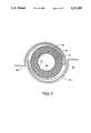
- each of the two hinges 82, 84is a spiral interlocking with the other hinge.
- metal traces 83a, 83b and heated bimetallic region 85are shown.
- the heatermay be a resistive heater formed for instance of a nickel alloy layer formed on top of the diaphragm. The width and spacing of the grooves and metal traces ar exaggerated in FIG. 7 for clarity.
- center hinge 110surrounding the center boss 112 portion of the microactuator to provide thermal isolation to the center boss 112 from the heated annular region 85.
- Center hinge 110is similar in structure to hinges 82 and 84 but is circular and not split, since no conductive traces cross hinge 110. Hinge 110 in addition to further insulating the heated region 85 reduces the thermal mass that needs to be heated, thereby speeding up operation of the microactuator. Additionally it is desirable to insulate the center boss because the thermal loss thereof depends on whether (in a valve) the microactuator is opened or closed, since in the closed position there is increased thermal conduction across the valve seat to the outside package. This results undesirably in thermal hysteresis in the valve. The center hinge greatly reduces this undesirable effect.
Landscapes
- Engineering & Computer Science (AREA)
- General Engineering & Computer Science (AREA)
- Mechanical Engineering (AREA)
- Chemical & Material Sciences (AREA)
- Dispersion Chemistry (AREA)
- Computer Hardware Design (AREA)
- Microelectronics & Electronic Packaging (AREA)
- Theoretical Computer Science (AREA)
- Physics & Mathematics (AREA)
- Fluid Mechanics (AREA)
- Temperature-Responsive Valves (AREA)
- Mechanical Light Control Or Optical Switches (AREA)
Abstract
Description
Claims (14)
Priority Applications (1)
| Application Number | Priority Date | Filing Date | Title |
|---|---|---|---|
| US07/891,354US5271597A (en) | 1992-05-29 | 1992-05-29 | Bimetallic diaphragm with split hinge for microactuator |
Applications Claiming Priority (1)
| Application Number | Priority Date | Filing Date | Title |
|---|---|---|---|
| US07/891,354US5271597A (en) | 1992-05-29 | 1992-05-29 | Bimetallic diaphragm with split hinge for microactuator |
Publications (1)
| Publication Number | Publication Date |
|---|---|
| US5271597Atrue US5271597A (en) | 1993-12-21 |
Family
ID=25398038
Family Applications (1)
| Application Number | Title | Priority Date | Filing Date |
|---|---|---|---|
| US07/891,354Expired - LifetimeUS5271597A (en) | 1992-05-29 | 1992-05-29 | Bimetallic diaphragm with split hinge for microactuator |
Country Status (1)
| Country | Link |
|---|---|
| US (1) | US5271597A (en) |
Cited By (41)
| Publication number | Priority date | Publication date | Assignee | Title |
|---|---|---|---|---|
| US5449569A (en)* | 1992-05-20 | 1995-09-12 | Schumm, Jr.; Brooke | Fluid depolarized battery with improved automatic valve |
| US5541016A (en)* | 1992-05-20 | 1996-07-30 | Schumm, Jr.; Brooke | Electrical appliance with automatic valve especially for fluid depolarized electrochemical battery |
| US5640995A (en)* | 1995-03-14 | 1997-06-24 | Baxter International Inc. | Electrofluidic standard module and custom circuit board assembly |
| US5748409A (en)* | 1995-03-08 | 1998-05-05 | Hutchinson Technology Incorporated | Welding stress isolation structure for head suspension assemblies |
| US5964239A (en)* | 1996-05-23 | 1999-10-12 | Hewlett-Packard Company | Housing assembly for micromachined fluid handling structure |
| US6041600A (en)* | 1997-07-15 | 2000-03-28 | Silverbrook Research Pty. Ltd | Utilization of quantum wires in MEMS actuators |
| US6044646A (en)* | 1997-07-15 | 2000-04-04 | Silverbrook Research Pty. Ltd. | Micro cilia array and use thereof |
| US6067797A (en)* | 1997-07-15 | 2000-05-30 | Silverbrook Research Pty, Ltd. | Thermal actuator |
| US6102068A (en)* | 1997-09-23 | 2000-08-15 | Hewlett-Packard Company | Selector valve assembly |
| EP1031735A2 (en) | 1999-02-23 | 2000-08-30 | Matsushita Electric Works, Ltd. | Microactuator |
| US6494433B2 (en) | 2000-06-06 | 2002-12-17 | The Regents Of The University Of Michigan | Thermally activated polymer device |
| US6494804B1 (en) | 2000-06-20 | 2002-12-17 | Kelsey-Hayes Company | Microvalve for electronically controlled transmission |
| US6523560B1 (en) | 1998-09-03 | 2003-02-25 | General Electric Corporation | Microvalve with pressure equalization |
| US6533366B1 (en) | 1996-05-29 | 2003-03-18 | Kelsey-Hayes Company | Vehicle hydraulic braking systems incorporating micro-machined technology |
| US6540203B1 (en) | 1999-03-22 | 2003-04-01 | Kelsey-Hayes Company | Pilot operated microvalve device |
| US6581640B1 (en) | 2000-08-16 | 2003-06-24 | Kelsey-Hayes Company | Laminated manifold for microvalve |
| US20030160538A1 (en)* | 1999-02-23 | 2003-08-28 | Matsushita Electric Works, Ltd. | Semiconductor device |
| US6612535B1 (en)* | 1997-01-24 | 2003-09-02 | California Institute Of Technology | MEMS valve |
| US6694998B1 (en) | 2000-03-22 | 2004-02-24 | Kelsey-Hayes Company | Micromachined structure usable in pressure regulating microvalve and proportional microvalve |
| US6761420B2 (en) | 1998-09-03 | 2004-07-13 | Ge Novasensor | Proportional micromechanical device |
| US6845962B1 (en) | 2000-03-22 | 2005-01-25 | Kelsey-Hayes Company | Thermally actuated microvalve device |
| US20050156129A1 (en)* | 1998-09-03 | 2005-07-21 | General Electric Company | Proportional micromechanical valve |
| US20060257701A1 (en)* | 2004-10-29 | 2006-11-16 | Schumm Brooke Jr | Fluid regulating microvalve assembly for fluid consuming cells |
| US7156365B2 (en) | 2004-07-27 | 2007-01-02 | Kelsey-Hayes Company | Method of controlling microvalve actuator |
| US20100019177A1 (en)* | 2006-12-15 | 2010-01-28 | Luckevich Mark S | Microvalve device |
| US7803281B2 (en) | 2004-03-05 | 2010-09-28 | Microstaq, Inc. | Selective bonding for forming a microvalve |
| US8011388B2 (en) | 2003-11-24 | 2011-09-06 | Microstaq, INC | Thermally actuated microvalve with multiple fluid ports |
| US8113482B2 (en) | 2008-08-12 | 2012-02-14 | DunAn Microstaq | Microvalve device with improved fluid routing |
| US8387659B2 (en) | 2007-03-31 | 2013-03-05 | Dunan Microstaq, Inc. | Pilot operated spool valve |
| US8393344B2 (en) | 2007-03-30 | 2013-03-12 | Dunan Microstaq, Inc. | Microvalve device with pilot operated spool valve and pilot microvalve |
| WO2013106714A1 (en) | 2012-01-13 | 2013-07-18 | Schumm Brooke Jr | Fluid regulating microvalve assembly for fluid consuming cells with spring-like shape-retaining aperture cover |
| US8540207B2 (en) | 2008-12-06 | 2013-09-24 | Dunan Microstaq, Inc. | Fluid flow control assembly |
| US8593811B2 (en) | 2009-04-05 | 2013-11-26 | Dunan Microstaq, Inc. | Method and structure for optimizing heat exchanger performance |
| US8662468B2 (en) | 2008-08-09 | 2014-03-04 | Dunan Microstaq, Inc. | Microvalve device |
| US8925793B2 (en) | 2012-01-05 | 2015-01-06 | Dunan Microstaq, Inc. | Method for making a solder joint |
| US8956884B2 (en) | 2010-01-28 | 2015-02-17 | Dunan Microstaq, Inc. | Process for reconditioning semiconductor surface to facilitate bonding |
| US8996141B1 (en) | 2010-08-26 | 2015-03-31 | Dunan Microstaq, Inc. | Adaptive predictive functional controller |
| US9006844B2 (en) | 2010-01-28 | 2015-04-14 | Dunan Microstaq, Inc. | Process and structure for high temperature selective fusion bonding |
| US9140613B2 (en) | 2012-03-16 | 2015-09-22 | Zhejiang Dunan Hetian Metal Co., Ltd. | Superheat sensor |
| US9188375B2 (en) | 2013-12-04 | 2015-11-17 | Zhejiang Dunan Hetian Metal Co., Ltd. | Control element and check valve assembly |
| US9702481B2 (en) | 2009-08-17 | 2017-07-11 | Dunan Microstaq, Inc. | Pilot-operated spool valve |
Citations (7)
| Publication number | Priority date | Publication date | Assignee | Title |
|---|---|---|---|---|
| US4318071A (en)* | 1980-04-04 | 1982-03-02 | Texas Instruments Incorporated | Interface relay for high current equipment |
| US4756508A (en)* | 1985-02-21 | 1988-07-12 | Ford Motor Company | Silicon valve |
| US4825262A (en)* | 1985-10-16 | 1989-04-25 | British Telecommunications Public Limited Company | Fabry-perot interferometer |
| US4859060A (en)* | 1985-11-26 | 1989-08-22 | 501 Sharp Kabushiki Kaisha | Variable interferometric device and a process for the production of the same |
| US4864824A (en)* | 1988-10-31 | 1989-09-12 | American Telephone And Telegraph Company, At&T Bell Laboratories | Thin film shape memory alloy and method for producing |
| US5058856A (en)* | 1991-05-08 | 1991-10-22 | Hewlett-Packard Company | Thermally-actuated microminiature valve |
| US5069419A (en)* | 1989-06-23 | 1991-12-03 | Ic Sensors Inc. | Semiconductor microactuator |
- 1992
- 1992-05-29USUS07/891,354patent/US5271597A/ennot_activeExpired - Lifetime
Patent Citations (7)
| Publication number | Priority date | Publication date | Assignee | Title |
|---|---|---|---|---|
| US4318071A (en)* | 1980-04-04 | 1982-03-02 | Texas Instruments Incorporated | Interface relay for high current equipment |
| US4756508A (en)* | 1985-02-21 | 1988-07-12 | Ford Motor Company | Silicon valve |
| US4825262A (en)* | 1985-10-16 | 1989-04-25 | British Telecommunications Public Limited Company | Fabry-perot interferometer |
| US4859060A (en)* | 1985-11-26 | 1989-08-22 | 501 Sharp Kabushiki Kaisha | Variable interferometric device and a process for the production of the same |
| US4864824A (en)* | 1988-10-31 | 1989-09-12 | American Telephone And Telegraph Company, At&T Bell Laboratories | Thin film shape memory alloy and method for producing |
| US5069419A (en)* | 1989-06-23 | 1991-12-03 | Ic Sensors Inc. | Semiconductor microactuator |
| US5058856A (en)* | 1991-05-08 | 1991-10-22 | Hewlett-Packard Company | Thermally-actuated microminiature valve |
Non-Patent Citations (4)
| Title |
|---|
| IEEE CH2783 9/90/0000 0065$01.00 1990, Hal Jerman Electrically Activated, Micromachined Diaphragm Valves .* |
| IEEE CH2783-9/90/0000-0065$01.00 1990, Hal Jerman "Electrically-Activated, Micromachined Diaphragm Valves". |
| IEEE Conf. Jun. 1991, Hal Jerman "Electrically-Activated, Normally-Closed Diaphragm Valves". |
| IEEE Conf. Jun. 1991, Hal Jerman Electrically Activated, Normally Closed Diaphragm Valves .* |
Cited By (52)
| Publication number | Priority date | Publication date | Assignee | Title |
|---|---|---|---|---|
| US5541016A (en)* | 1992-05-20 | 1996-07-30 | Schumm, Jr.; Brooke | Electrical appliance with automatic valve especially for fluid depolarized electrochemical battery |
| US5449569A (en)* | 1992-05-20 | 1995-09-12 | Schumm, Jr.; Brooke | Fluid depolarized battery with improved automatic valve |
| US5748409A (en)* | 1995-03-08 | 1998-05-05 | Hutchinson Technology Incorporated | Welding stress isolation structure for head suspension assemblies |
| US5640995A (en)* | 1995-03-14 | 1997-06-24 | Baxter International Inc. | Electrofluidic standard module and custom circuit board assembly |
| US5964239A (en)* | 1996-05-23 | 1999-10-12 | Hewlett-Packard Company | Housing assembly for micromachined fluid handling structure |
| US6533366B1 (en) | 1996-05-29 | 2003-03-18 | Kelsey-Hayes Company | Vehicle hydraulic braking systems incorporating micro-machined technology |
| US6612535B1 (en)* | 1997-01-24 | 2003-09-02 | California Institute Of Technology | MEMS valve |
| US6041600A (en)* | 1997-07-15 | 2000-03-28 | Silverbrook Research Pty. Ltd | Utilization of quantum wires in MEMS actuators |
| US6044646A (en)* | 1997-07-15 | 2000-04-04 | Silverbrook Research Pty. Ltd. | Micro cilia array and use thereof |
| US6067797A (en)* | 1997-07-15 | 2000-05-30 | Silverbrook Research Pty, Ltd. | Thermal actuator |
| US6102068A (en)* | 1997-09-23 | 2000-08-15 | Hewlett-Packard Company | Selector valve assembly |
| US7367359B2 (en) | 1998-09-03 | 2008-05-06 | Kelsey-Hayes Company | Proportional micromechanical valve |
| US7011378B2 (en) | 1998-09-03 | 2006-03-14 | Ge Novasensor, Inc. | Proportional micromechanical valve |
| US6523560B1 (en) | 1998-09-03 | 2003-02-25 | General Electric Corporation | Microvalve with pressure equalization |
| US20050156129A1 (en)* | 1998-09-03 | 2005-07-21 | General Electric Company | Proportional micromechanical valve |
| US6761420B2 (en) | 1998-09-03 | 2004-07-13 | Ge Novasensor | Proportional micromechanical device |
| US6384509B1 (en) | 1999-02-23 | 2002-05-07 | Matsushita Electric Works, Ltd. | Semiconductor device |
| US20030160538A1 (en)* | 1999-02-23 | 2003-08-28 | Matsushita Electric Works, Ltd. | Semiconductor device |
| US6791233B2 (en) | 1999-02-23 | 2004-09-14 | Matsushita Electric Works, Ltd. | Semiconductor device |
| EP1031735A3 (en)* | 1999-02-23 | 2004-04-07 | Matsushita Electric Works, Ltd. | Microactuator |
| EP1031735A2 (en) | 1999-02-23 | 2000-08-30 | Matsushita Electric Works, Ltd. | Microactuator |
| US6540203B1 (en) | 1999-03-22 | 2003-04-01 | Kelsey-Hayes Company | Pilot operated microvalve device |
| US6994115B2 (en) | 2000-03-22 | 2006-02-07 | Kelsey-Hayes Company | Thermally actuated microvalve device |
| US6845962B1 (en) | 2000-03-22 | 2005-01-25 | Kelsey-Hayes Company | Thermally actuated microvalve device |
| US6694998B1 (en) | 2000-03-22 | 2004-02-24 | Kelsey-Hayes Company | Micromachined structure usable in pressure regulating microvalve and proportional microvalve |
| US6494433B2 (en) | 2000-06-06 | 2002-12-17 | The Regents Of The University Of Michigan | Thermally activated polymer device |
| US6494804B1 (en) | 2000-06-20 | 2002-12-17 | Kelsey-Hayes Company | Microvalve for electronically controlled transmission |
| US6581640B1 (en) | 2000-08-16 | 2003-06-24 | Kelsey-Hayes Company | Laminated manifold for microvalve |
| US8011388B2 (en) | 2003-11-24 | 2011-09-06 | Microstaq, INC | Thermally actuated microvalve with multiple fluid ports |
| US7803281B2 (en) | 2004-03-05 | 2010-09-28 | Microstaq, Inc. | Selective bonding for forming a microvalve |
| US7156365B2 (en) | 2004-07-27 | 2007-01-02 | Kelsey-Hayes Company | Method of controlling microvalve actuator |
| US20060257701A1 (en)* | 2004-10-29 | 2006-11-16 | Schumm Brooke Jr | Fluid regulating microvalve assembly for fluid consuming cells |
| US7378168B2 (en) | 2004-10-29 | 2008-05-27 | Eveready Battery Company, Inc. | Fluid regulating microvalve assembly for fluid consuming cells |
| US20080160373A1 (en)* | 2004-10-29 | 2008-07-03 | Brooke Schumm | Fluid regulating microvalve assembly for fluid consuming cells |
| US20100019177A1 (en)* | 2006-12-15 | 2010-01-28 | Luckevich Mark S | Microvalve device |
| US8156962B2 (en) | 2006-12-15 | 2012-04-17 | Dunan Microstaq, Inc. | Microvalve device |
| US8393344B2 (en) | 2007-03-30 | 2013-03-12 | Dunan Microstaq, Inc. | Microvalve device with pilot operated spool valve and pilot microvalve |
| US8387659B2 (en) | 2007-03-31 | 2013-03-05 | Dunan Microstaq, Inc. | Pilot operated spool valve |
| US8662468B2 (en) | 2008-08-09 | 2014-03-04 | Dunan Microstaq, Inc. | Microvalve device |
| US8113482B2 (en) | 2008-08-12 | 2012-02-14 | DunAn Microstaq | Microvalve device with improved fluid routing |
| US8540207B2 (en) | 2008-12-06 | 2013-09-24 | Dunan Microstaq, Inc. | Fluid flow control assembly |
| US8593811B2 (en) | 2009-04-05 | 2013-11-26 | Dunan Microstaq, Inc. | Method and structure for optimizing heat exchanger performance |
| US9702481B2 (en) | 2009-08-17 | 2017-07-11 | Dunan Microstaq, Inc. | Pilot-operated spool valve |
| US8956884B2 (en) | 2010-01-28 | 2015-02-17 | Dunan Microstaq, Inc. | Process for reconditioning semiconductor surface to facilitate bonding |
| US9006844B2 (en) | 2010-01-28 | 2015-04-14 | Dunan Microstaq, Inc. | Process and structure for high temperature selective fusion bonding |
| US8996141B1 (en) | 2010-08-26 | 2015-03-31 | Dunan Microstaq, Inc. | Adaptive predictive functional controller |
| US8925793B2 (en) | 2012-01-05 | 2015-01-06 | Dunan Microstaq, Inc. | Method for making a solder joint |
| WO2013106714A1 (en) | 2012-01-13 | 2013-07-18 | Schumm Brooke Jr | Fluid regulating microvalve assembly for fluid consuming cells with spring-like shape-retaining aperture cover |
| US9140613B2 (en) | 2012-03-16 | 2015-09-22 | Zhejiang Dunan Hetian Metal Co., Ltd. | Superheat sensor |
| US9404815B2 (en) | 2012-03-16 | 2016-08-02 | Zhejiang Dunan Hetian Metal Co., Ltd. | Superheat sensor having external temperature sensor |
| US9772235B2 (en) | 2012-03-16 | 2017-09-26 | Zhejiang Dunan Hetian Metal Co., Ltd. | Method of sensing superheat |
| US9188375B2 (en) | 2013-12-04 | 2015-11-17 | Zhejiang Dunan Hetian Metal Co., Ltd. | Control element and check valve assembly |
Similar Documents
| Publication | Publication Date | Title |
|---|---|---|
| US5271597A (en) | Bimetallic diaphragm with split hinge for microactuator | |
| EP0478716B1 (en) | Semiconductor microactuator | |
| US6275320B1 (en) | MEMS variable optical attenuator | |
| EP1317399B1 (en) | Microelectromechanical flexible membrane electrostatic valve device and related fabrication methods | |
| KR20010050447A (en) | In-plane MEMS thermal actuator and associated fabrication methods | |
| JPH08114278A (en) | Micro-actuator | |
| JP3041538B2 (en) | Electronic microvalve device and method of manufacturing the same | |
| US6496351B2 (en) | MEMS device members having portions that contact a substrate and associated methods of operating | |
| EP1183566B1 (en) | Micromachined electrostatic actuator with air gap | |
| JPH05187574A (en) | Microminiature valve | |
| JP4030967B2 (en) | Microfabricated element provided with thermoelectric element and manufacturing method thereof | |
| EP1461816B1 (en) | Mems device having contact and standoff bumps and related methods | |
| US7622783B2 (en) | MEMS thermal actuator and method of manufacture | |
| US5467068A (en) | Micromachined bi-material signal switch | |
| KR20010031838A (en) | Microelectromechanical positioning apparatus | |
| JP2001296483A (en) | Article consisting of optical hollow | |
| US6765300B1 (en) | Micro-relay | |
| US5467067A (en) | Thermally actuated micromachined microwave switch | |
| US7034375B2 (en) | Micro electromechanical systems thermal switch | |
| CN112271105B (en) | A kind of MEMS thermal protector and preparation method thereof | |
| GB2295441A (en) | Microminature fluid flow device | |
| CN112260218B (en) | Overcurrent protector with adjustable rated current and capable of being monitored and preparation method | |
| JP2003120851A (en) | Semiconductor microvalve | |
| JP2025099577A (en) | Method for manufacturing sensor device and sensor device |
Legal Events
| Date | Code | Title | Description |
|---|---|---|---|
| AS | Assignment | Owner name:IC SENSORS, INC. A CORP. OF CA, CALIFORNIA Free format text:ASSIGNMENT OF ASSIGNORS INTEREST.;ASSIGNOR:JERMAN, JOHN H.;REEL/FRAME:006153/0884 Effective date:19920527 | |
| FEPP | Fee payment procedure | Free format text:PAYOR NUMBER ASSIGNED (ORIGINAL EVENT CODE: ASPN); ENTITY STATUS OF PATENT OWNER: LARGE ENTITY | |
| STCF | Information on status: patent grant | Free format text:PATENTED CASE | |
| AS | Assignment | Owner name:SILICON VALLEY BANK, CALIFORNIA Free format text:SECURITY INTEREST;ASSIGNOR:IC SENSORS, INC.;REEL/FRAME:007077/0910 Effective date:19940317 | |
| CC | Certificate of correction | ||
| FEPP | Fee payment procedure | Free format text:PAYOR NUMBER ASSIGNED (ORIGINAL EVENT CODE: ASPN); ENTITY STATUS OF PATENT OWNER: LARGE ENTITY Free format text:PAYER NUMBER DE-ASSIGNED (ORIGINAL EVENT CODE: RMPN); ENTITY STATUS OF PATENT OWNER: LARGE ENTITY | |
| FPAY | Fee payment | Year of fee payment:4 | |
| AS | Assignment | Owner name:PNC BANK, NATIONAL ASSOCIATIONS, NEW JERSEY Free format text:SECURITY INTEREST;ASSIGNOR:IC SENSORS, INC;REEL/FRAME:011027/0792 Effective date:20000215 | |
| AS | Assignment | Owner name:IC SENSORS, INC., CALIFORNIA Free format text:RELEASE BY SECURED PARTY;ASSIGNOR:SILICON VALLEY BANK;REEL/FRAME:010832/0438 Effective date:19940317 | |
| AS | Assignment | Owner name:FIRST UNION NATIONAL BANK, AS AGENT, NEW JERSEY Free format text:SECURITY INTEREST;ASSIGNOR:IC SENSORS, INC.;REEL/FRAME:011284/0293 Effective date:20000807 | |
| FPAY | Fee payment | Year of fee payment:8 | |
| REMI | Maintenance fee reminder mailed | ||
| AS | Assignment | Owner name:FLEET CAPITAL CORPORATION, TEXAS Free format text:SECURITY AGREEMENT;ASSIGNORS:MEASUREMENT SPECIALTIES, INC.;IC SENSORS, INC.;REEL/FRAME:013845/0001 Effective date:20030131 Owner name:IC SENSORS, INC., NEW JERSEY Free format text:RELEASE OF SECURITY INTEREST IN PATENTS AND TRADEM;ASSIGNOR:WACHOVIA BANK, NATIONAL ASSOCIATION;REEL/FRAME:013879/0721 Effective date:20030130 Owner name:MEASUREMENTSPECIALTIES, INC., NEW JERSEY Free format text:RELEASE OF SECURITY INTEREST IN PATENTS AND TRADEM;ASSIGNOR:WACHOVIA BANK, NATIONAL ASSOCIATION;REEL/FRAME:013879/0721 Effective date:20030130 | |
| FEPP | Fee payment procedure | Free format text:PAYOR NUMBER ASSIGNED (ORIGINAL EVENT CODE: ASPN); ENTITY STATUS OF PATENT OWNER: LARGE ENTITY Free format text:PAYER NUMBER DE-ASSIGNED (ORIGINAL EVENT CODE: RMPN); ENTITY STATUS OF PATENT OWNER: LARGE ENTITY | |
| FEPP | Fee payment procedure | Free format text:PAYER NUMBER DE-ASSIGNED (ORIGINAL EVENT CODE: RMPN); ENTITY STATUS OF PATENT OWNER: LARGE ENTITY Free format text:PAYOR NUMBER ASSIGNED (ORIGINAL EVENT CODE: ASPN); ENTITY STATUS OF PATENT OWNER: LARGE ENTITY | |
| AS | Assignment | Owner name:GENERAL ELECTRIC CAPITAL CORPORATION, CONNECTICUT Free format text:SECURITY AGREEMENT;ASSIGNOR:MEASUREMENT SPECIALTIES, INC.;REEL/FRAME:016153/0714 Effective date:20041217 Owner name:MEASUREMENT SPECIALTIES, INC., NEW JERSEY Free format text:RELEASE OF SECURITY INTEREST;ASSIGNOR:FLEET CAPITAL CORPORATION;REEL/FRAME:016824/0143 Effective date:20041217 Owner name:IC SENSORS, INC., NEW JERSEY Free format text:RELEASE OF SECURITY INTEREST;ASSIGNOR:FLEET CAPITAL CORPORATION;REEL/FRAME:016824/0143 Effective date:20041217 | |
| FPAY | Fee payment | Year of fee payment:12 | |
| AS | Assignment | Owner name:IC SENSORS, INC., NEW JERSEY Free format text:RELEASE BY SECURED PARTY;ASSIGNOR:FLEET CAPITAL CORPORATION;REEL/FRAME:016800/0587 Effective date:20041217 Owner name:MEASUREMENT SPECIALTIES, INC., NEW JERSEY Free format text:RELEASE BY SECURED PARTY;ASSIGNOR:FLEET CAPITAL CORPORATION;REEL/FRAME:016800/0587 Effective date:20041217 | |
| AS | Assignment | Owner name:JPMORGAN CHASE BANK, N.A., AS COLLATERAL AGENT,ILL Free format text:SECURITY AGREEMENT;ASSIGNOR:IC SENSORS, INC.;REEL/FRAME:024463/0944 Effective date:20100601 | |
| AS | Assignment | Owner name:MEASUREMENT SPECIALTIES, INC.,VIRGINIA Free format text:RELEASE BY SECURED PARTY;ASSIGNOR:GENERAL ELECTRIC CAPITAL CORPORATION;REEL/FRAME:024474/0377 Effective date:20100601 Owner name:IC SENSORS, INC.,VIRGINIA Free format text:RELEASE BY SECURED PARTY;ASSIGNOR:GENERAL ELECTRIC CAPITAL CORPORATION;REEL/FRAME:024474/0377 Effective date:20100601 Owner name:ELEKON INDUSTRIES USA, INC.,VIRGINIA Free format text:RELEASE BY SECURED PARTY;ASSIGNOR:GENERAL ELECTRIC CAPITAL CORPORATION;REEL/FRAME:024474/0377 Effective date:20100601 Owner name:ENTRAN DEVICES LLC,VIRGINIA Free format text:RELEASE BY SECURED PARTY;ASSIGNOR:GENERAL ELECTRIC CAPITAL CORPORATION;REEL/FRAME:024474/0377 Effective date:20100601 Owner name:MEASUREMENT SPECIALTIES FOREIGN HOLDINGS CORPORATI Free format text:RELEASE BY SECURED PARTY;ASSIGNOR:GENERAL ELECTRIC CAPITAL CORPORATION;REEL/FRAME:024474/0377 Effective date:20100601 Owner name:YSIS INCORPORATED,VIRGINIA Free format text:RELEASE BY SECURED PARTY;ASSIGNOR:GENERAL ELECTRIC CAPITAL CORPORATION;REEL/FRAME:024474/0377 Effective date:20100601 Owner name:MREHTATEB, LLC LIMITED LIABILITY COMPANY - MASSACH Free format text:RELEASE BY SECURED PARTY;ASSIGNOR:GENERAL ELECTRIC CAPITAL CORPORATION;REEL/FRAME:024474/0377 Effective date:20100601 | |
| AS | Assignment | Owner name:I C SENSORS INC., NEW JERSEY Free format text:RELEASE OF LIEN ON PATENTS;ASSIGNOR:PNC BANK NATIONAL ASSOCIATION;REEL/FRAME:026673/0060 Effective date:20110721 | |
| AS | Assignment | Owner name:IC SENSORS, INC., VIRGINIA Free format text:RELEASE OF PATENT SECURITY INTEREST;ASSIGNOR:JPMORGAN CHASE BANK, N.A., AS COLLATERAL AGENT;REEL/FRAME:034104/0170 Effective date:20141009 |